NanoStar & NanoFree 300 m Solder Bump Wafer Chip … · SBVA017 NanoStar & NanoFree 300 m Solder...
22
Application Report SBVA017 - February 2004 1 NanoStart & NanoFreet 300mm Solder Bump Wafer Chip-Scale Package Application Jim Rosson High Performance Analog—MAKE Packaging ABSTRACT The NanoStartWafer Chip-Scale Package (WCSP) is a family of bare die packages developed for applications that require the smallest possible package. WCSP provides electrical interconnection via solder spheres attached to the die and is aligned with JEDEC package standard MO-211[1]. NanoStar, with advanced materials engineering technology, has demonstrated excellent board level reliability that allows it to be used without the need for underfill adhesives, unlike conventional solder-bumped Flip Chip devices. This advanced design allows standard, low-cost surface-mount technology (SMT) assembly processes to be used successfully. This application guide provides the necessary design and reliability information to apply the NanoStar 300µm solder bump packages. Contents 1 Introduction 3 . . . . . . . . . . . . . . . . . . . . . . . . . . . . . . . . . . . . . . . . . . . . . . . . . . . . . . . . . . . . . . . . . . . . . . . . 1.1 Package Offerings and Nomenclature 4 . . . . . . . . . . . . . . . . . . . . . . . . . . . . . . . . . . . . . . . . . . . . . . 2 Physical Description 5 . . . . . . . . . . . . . . . . . . . . . . . . . . . . . . . . . . . . . . . . . . . . . . . . . . . . . . . . . . . . . . . . 2.1 Package Characteristics 5 . . . . . . . . . . . . . . . . . . . . . . . . . . . . . . . . . . . . . . . . . . . . . . . . . . . . . . . . . . 2.2 NanoStar Package Dimensions 6 . . . . . . . . . . . . . . . . . . . . . . . . . . . . . . . . . . . . . . . . . . . . . . . . . . . 2.3 Thermal Performance 8 . . . . . . . . . . . . . . . . . . . . . . . . . . . . . . . . . . . . . . . . . . . . . . . . . . . . . . . . . . . . 2.4 Board Level Reliability 10 . . . . . . . . . . . . . . . . . . . . . . . . . . . . . . . . . . . . . . . . . . . . . . . . . . . . . . . . . . 3 Printed Circuit Board Assembly 13 . . . . . . . . . . . . . . . . . . . . . . . . . . . . . . . . . . . . . . . . . . . . . . . . . . . . 3.1 PCB Design Guidelines 13 . . . . . . . . . . . . . . . . . . . . . . . . . . . . . . . . . . . . . . . . . . . . . . . . . . . . . . . . . 3.2 PCB Land Pattern Recommendations 14 . . . . . . . . . . . . . . . . . . . . . . . . . . . . . . . . . . . . . . . . . . . . . 3.3 Solder Paste Stencil Design 15 . . . . . . . . . . . . . . . . . . . . . . . . . . . . . . . . . . . . . . . . . . . . . . . . . . . . . 3.4 Component Placement 15 . . . . . . . . . . . . . . . . . . . . . . . . . . . . . . . . . . . . . . . . . . . . . . . . . . . . . . . . . . 3.5 Reflow 16 . . . . . . . . . . . . . . . . . . . . . . . . . . . . . . . . . . . . . . . . . . . . . . . . . . . . . . . . . . . . . . . . . . . . . . . . 4 Tape and Reel Information 17 . . . . . . . . . . . . . . . . . . . . . . . . . . . . . . . . . . . . . . . . . . . . . . . . . . . . . . . . . . 4.1 Material Specifications 17 . . . . . . . . . . . . . . . . . . . . . . . . . . . . . . . . . . . . . . . . . . . . . . . . . . . . . . . . . . 5 Symbolization 19 . . . . . . . . . . . . . . . . . . . . . . . . . . . . . . . . . . . . . . . . . . . . . . . . . . . . . . . . . . . . . . . . . . . . . 6 Features and Benefits 20 . . . . . . . . . . . . . . . . . . . . . . . . . . . . . . . . . . . . . . . . . . . . . . . . . . . . . . . . . . . . . . 7 Conclusion 21 . . . . . . . . . . . . . . . . . . . . . . . . . . . . . . . . . . . . . . . . . . . . . . . . . . . . . . . . . . . . . . . . . . . . . . . . Acknowledgments 21 . . . . . . . . . . . . . . . . . . . . . . . . . . . . . . . . . . . . . . . . . . . . . . . . . . . . . . . . . . . . . . . . . . . . . References 21 . . . . . . . . . . . . . . . . . . . . . . . . . . . . . . . . . . . . . . . . . . . . . . . . . . . . . . . . . . . . . . . . . . . . . . . . . . . . Trademarks are the property of their respective owners.
Transcript of NanoStar & NanoFree 300 m Solder Bump Wafer Chip … · SBVA017 NanoStar & NanoFree 300 m Solder...

Application ReportSBVA017 - February 2004
1
NanoStar & NanoFree 300m Solder Bump WaferChip-Scale Package Application
Jim Rosson High Performance Analog—MAKE Packaging
ABSTRACT
The NanoStarWafer Chip-Scale Package (WCSP) is a family of bare die packagesdeveloped for applications that require the smallest possible package. WCSP provideselectrical interconnection via solder spheres attached to the die and is aligned with JEDECpackage standard MO−211[1]. NanoStar, with advanced materials engineering technology,has demonstrated excellent board level reliability that allows it to be used without the need forunderfill adhesives, unlike conventional solder-bumped Flip Chip devices. This advanceddesign allows standard, low-cost surface-mount technology (SMT) assembly processes tobe used successfully. This application guide provides the necessary design and reliabilityinformation to apply the NanoStar 300µm solder bump packages.
Contents
1 Introduction 3 . . . . . . . . . . . . . . . . . . . . . . . . . . . . . . . . . . . . . . . . . . . . . . . . . . . . . . . . . . . . . . . . . . . . . . . . 1.1 Package Offerings and Nomenclature 4 . . . . . . . . . . . . . . . . . . . . . . . . . . . . . . . . . . . . . . . . . . . . . .
2 Physical Description 5 . . . . . . . . . . . . . . . . . . . . . . . . . . . . . . . . . . . . . . . . . . . . . . . . . . . . . . . . . . . . . . . . 2.1 Package Characteristics 5 . . . . . . . . . . . . . . . . . . . . . . . . . . . . . . . . . . . . . . . . . . . . . . . . . . . . . . . . . . 2.2 NanoStar Package Dimensions 6 . . . . . . . . . . . . . . . . . . . . . . . . . . . . . . . . . . . . . . . . . . . . . . . . . . . 2.3 Thermal Performance 8 . . . . . . . . . . . . . . . . . . . . . . . . . . . . . . . . . . . . . . . . . . . . . . . . . . . . . . . . . . . . 2.4 Board Level Reliability 10 . . . . . . . . . . . . . . . . . . . . . . . . . . . . . . . . . . . . . . . . . . . . . . . . . . . . . . . . . .
3 Printed Circuit Board Assembly 13 . . . . . . . . . . . . . . . . . . . . . . . . . . . . . . . . . . . . . . . . . . . . . . . . . . . . 3.1 PCB Design Guidelines 13 . . . . . . . . . . . . . . . . . . . . . . . . . . . . . . . . . . . . . . . . . . . . . . . . . . . . . . . . . 3.2 PCB Land Pattern Recommendations 14 . . . . . . . . . . . . . . . . . . . . . . . . . . . . . . . . . . . . . . . . . . . . . 3.3 Solder Paste Stencil Design 15 . . . . . . . . . . . . . . . . . . . . . . . . . . . . . . . . . . . . . . . . . . . . . . . . . . . . . 3.4 Component Placement 15 . . . . . . . . . . . . . . . . . . . . . . . . . . . . . . . . . . . . . . . . . . . . . . . . . . . . . . . . . . 3.5 Reflow 16 . . . . . . . . . . . . . . . . . . . . . . . . . . . . . . . . . . . . . . . . . . . . . . . . . . . . . . . . . . . . . . . . . . . . . . . .
4 Tape and Reel Information 17 . . . . . . . . . . . . . . . . . . . . . . . . . . . . . . . . . . . . . . . . . . . . . . . . . . . . . . . . . . 4.1 Material Specifications 17 . . . . . . . . . . . . . . . . . . . . . . . . . . . . . . . . . . . . . . . . . . . . . . . . . . . . . . . . . .
5 Symbolization 19 . . . . . . . . . . . . . . . . . . . . . . . . . . . . . . . . . . . . . . . . . . . . . . . . . . . . . . . . . . . . . . . . . . . . .
6 Features and Benefits 20 . . . . . . . . . . . . . . . . . . . . . . . . . . . . . . . . . . . . . . . . . . . . . . . . . . . . . . . . . . . . . .
7 Conclusion 21 . . . . . . . . . . . . . . . . . . . . . . . . . . . . . . . . . . . . . . . . . . . . . . . . . . . . . . . . . . . . . . . . . . . . . . . .
Acknowledgments 21 . . . . . . . . . . . . . . . . . . . . . . . . . . . . . . . . . . . . . . . . . . . . . . . . . . . . . . . . . . . . . . . . . . . . .
References 21 . . . . . . . . . . . . . . . . . . . . . . . . . . . . . . . . . . . . . . . . . . . . . . . . . . . . . . . . . . . . . . . . . . . . . . . . . . . .
Trademarks are the property of their respective owners.
SBVA017
2 NanoStar & NanoFree 300m Solder Bump Wafer Chip-Scale Package Application
List of Figures
Figure 1. NanoStarWCSP, SOT−23, & SC−70 Size Comparison 3 . . . . . . . . . . . . . . . . . . . . . . . . . . . . . . Figure 2. NanoStar WCSP 5 . . . . . . . . . . . . . . . . . . . . . . . . . . . . . . . . . . . . . . . . . . . . . . . . . . . . . . . . . . . . . . . . Figure 3. Direct Bump WCSP Construction Cross-Section 5 . . . . . . . . . . . . . . . . . . . . . . . . . . . . . . . . . . . . Figure 4. RDL WCSP Construction Cross-Section 6 . . . . . . . . . . . . . . . . . . . . . . . . . . . . . . . . . . . . . . . . . . . Figure 5. YEB Package Dimensions 7 . . . . . . . . . . . . . . . . . . . . . . . . . . . . . . . . . . . . . . . . . . . . . . . . . . . . . . . . Figure 6. JEDEC 1S0P Thermal Performance Data Graph 8 . . . . . . . . . . . . . . . . . . . . . . . . . . . . . . . . . . . . Figure 7. JEDEC 2S2P Thermal Performance Data Graph 8 . . . . . . . . . . . . . . . . . . . . . . . . . . . . . . . . . . . . Figure 8. N25 5x5 Pin Array, 3.1mm Square, Daisy-Chain Test Die Diagram 11 . . . . . . . . . . . . . . . . . . . . Figure 9. N12 3x4 Pin Array, 2.14mm x 1.5mm, Daisy-Chain Test Die Diagram 11 . . . . . . . . . . . . . . . . . Figure 10. 12-Site Thermal Cycle Test BLR Test Board 11 . . . . . . . . . . . . . . . . . . . . . . . . . . . . . . . . . . . . . . Figure 11. N25 TCT Weibull Comparison of Ramp Rates and Materials 12 . . . . . . . . . . . . . . . . . . . . . . . . Figure 12. Typical Tin-Lead BLR Solder Fatigue Crack 13 . . . . . . . . . . . . . . . . . . . . . . . . . . . . . . . . . . . . . . Figure 13. Enlargement of Crack Area in Figure 12 13 . . . . . . . . . . . . . . . . . . . . . . . . . . . . . . . . . . . . . . . . . . Figure 14. Typical Lead-Free BLR Solder Fatigue Crack 13 . . . . . . . . . . . . . . . . . . . . . . . . . . . . . . . . . . . . . Figure 15. Enlargement of Crack Area in Figure 14 13 . . . . . . . . . . . . . . . . . . . . . . . . . . . . . . . . . . . . . . . . . . Figure 16. Example of 5x5 Array Balanced Routing Pattern 14 . . . . . . . . . . . . . . . . . . . . . . . . . . . . . . . . . . Figure 17. Recommended Solder Land Pattern Outline 15 . . . . . . . . . . . . . . . . . . . . . . . . . . . . . . . . . . . . . . Figure 18. Recommended Reflow Profiles 16 . . . . . . . . . . . . . . . . . . . . . . . . . . . . . . . . . . . . . . . . . . . . . . . . . Figure 19. Pocket Tape Dimensions 17 . . . . . . . . . . . . . . . . . . . . . . . . . . . . . . . . . . . . . . . . . . . . . . . . . . . . . . . Figure 20. Pocket Tape Dimensions 18 . . . . . . . . . . . . . . . . . . . . . . . . . . . . . . . . . . . . . . . . . . . . . . . . . . . . . . . Figure 21. Carrier-Tape Cavity Quadrant Location for Pin 1, per EIA−481B 19 . . . . . . . . . . . . . . . . . . . . .
List of Tables
Table 1. NanoStar & NanoFree 300µm Solder Bump Package Family Summary 4. . . . . . . . . . . . . . . Table 2. Simulated Thermal Resistance Data 9 . . . . . . . . . . . . . . . . . . . . . . . . . . . . . . . . . . . . . . . . . . . . . . . Table 3. Board-Level Reliability Test Matrix 10 . . . . . . . . . . . . . . . . . . . . . . . . . . . . . . . . . . . . . . . . . . . . . . . . . Table 4. NanoStar Board Level Reliability Summary 12 . . . . . . . . . . . . . . . . . . . . . . . . . . . . . . . . . . . . . . . . . Table 5. Recommended PCB Solder Land Pattern 14 . . . . . . . . . . . . . . . . . . . . . . . . . . . . . . . . . . . . . . . . . . Table 6. Recommended Solder Stencil Pattern 15 . . . . . . . . . . . . . . . . . . . . . . . . . . . . . . . . . . . . . . . . . . . . . Table 7. Recommended Critical Reflow Parameters 17 . . . . . . . . . . . . . . . . . . . . . . . . . . . . . . . . . . . . . . . . . Table 8. Common Tape Dimensions by Designator 18 . . . . . . . . . . . . . . . . . . . . . . . . . . . . . . . . . . . . . . . . . . Table 9. Reel Specifications 18 . . . . . . . . . . . . . . . . . . . . . . . . . . . . . . . . . . . . . . . . . . . . . . . . . . . . . . . . . . . . . . Table 10. Device-Marking Guidelines 19 . . . . . . . . . . . . . . . . . . . . . . . . . . . . . . . . . . . . . . . . . . . . . . . . . . . . .

SBVA017
3 NanoStar & NanoFree 300m Solder Bump Wafer Chip-Scale Package Application
1 Introduction
In today’s mobile environment, there seems to be an insatiable market demand for the smallestand lightest possible electronic products with high reliability. Electronics manufacturers are de-signing smaller and smaller products with each generation and release. Many different types ofpackages have been developed to meet this need. Popular package sizes such as MSOP,SOT−23, SC−70, and QFN outlines are quite large in comparison to a die size or wafer-levelchip-scale package. (See Figure 1.) There are several names for die size packages, includingFlip Chip (FC), Wafer-Level Chip Scale Package (WLCSP), and Wafer Scale Package (WSP).Regardless of the package name, however, the benefits to a die size package are clear: thesmallest possible form factor for an integrated circuit silicon die is the die itself.
TI utilizes new advanced polymer technology materials to enhance the board-level reliability ofthe NanoStar300µm solder ball packages. Many suppliers of WCSP packages use relativelybrittle re-passivation polymeric materials. While these brittle materials work well for some ap-plications, they have been shown to have poorer performance for 300µm solder sphere-bumpeddevices.[2] As a result of the new polymer technology available in the NanoStar package, TIcustomers do not have to experience premature device or reliability failures caused by brittle re-passivation and often seen in competitive parts.
Bottom
SC−70
TopNanoStar
Bottom
Top
SOT−23
Figure 1. NanoStar WCSP, SOT−23, & SC−70 Size Comparison
There are many challenges in interconnecting the micron-level world of silicon to enable bare dieuse in the millimeter-based world of SMT assembly. The proper system design for a die sizepackage application is critical. NanoStar WCSP has been developed in 4−36 pin packages toenable high performance products to be as small as possible. A summary of the available pack-ages is provided in Section 1.1. This package size not only enables smaller products, but alsoprovides improved electrical performance. The performance increase is a direct result of shorterinterconnections and, consequently, reduced parasitic losses due to interconnect length.

SBVA017
4 NanoStar & NanoFree 300m Solder Bump Wafer Chip-Scale Package Application
NanoStar WCSP adds other visible features, as well. All NanoStar devices are laser-marked toprovide device identification and production lot tracking. Most analog NanoStar devices alsohave a protective backside surface coating to improve performance. This opaque coatingreduces the parametric shifts that can occur due to the light sensitivity of IC structures. Thecoating allows a WCSP to provide the same level of consistent performance obtained from amolded package device.
This application note provides the necessary information to apply NanoStar technology withmaximum success. The enclosed mechanical, electrical, and thermal package information, inaddition to printed circuit board (PCB) design recommendations and reliability data, are the cul-mination of another enabling technology developed for Texas Instruments’ customers.
1.1 Package Offerings and Nomenclature
Table 1 shows the initial NanoStar WCSP package family lineup. As customer demandincreases and more devices use the TI WCSP, this list is expected to grow. Please visit the TIweb site for the latest list of products that use the NanoStar package family.
While the NanoStar name covers this entire WCSP family, TI also uses the NanoFree term todifferentiate devices that are available in lead-free solder alloys. For ease of reading, this docu-ment applies to both versions, and will typically use only the NanoStar name. Where differencesare noted for lead-free packages, the NanoFree name will be specifically inserted.
Table 1. NanoStar & NanoFree 300µm Solder Bump Package Family Summary (1)
Package Designator (2) Minimum “D” Maximum “D” Minimum “E” Maximum “E” Array Pinout
YEB, YZB 0.85 1.65 0.85 1.65 4
YEC, YZC 1.35 2.15 0.85 1.65 6
YED, YZD 1.85 2.65 0.85 1.65 8
YEF, YZF 1.35 2.15 1.35 2.15 9
YEG, YZG 1.85 2.65 1.35 2.15 12
YEH, YZH 1.85 2.65 1.85 2.65 16
YEJ, YZJ 2.35 3.15 1.85 2.65 20
YEK, YZK 2.35 3.15 2.35 3.15 25
YEL, YZL 2.35 3.65 2.35 3.15 30
YEM, YZM 2.85 3.65 2.85 3.65 36
YEU, YZU(3) 0.95 1.45 1.25 1.75 5
NOTE 1: Package availability varies based on currently released products. Some of the above packages may not be available. Pleasereference the TI web site (www.ti.com) for released packages.
NOTE 2: A Z designator indicates NanoFree devices.NOTE 3: Staggered array device.
The NanoStar WCSP packages in this report are referred to as simply NanoStar or WCSPpackages. The NanoStar 300µm package family currently encompasses the three-letter TIpackage designators YEB, YEC, YED, YEF, YEG, YEH, YEJ, YEK, YEL, YEM and YEU fortin-lead solder bumped devices. NanoFreeLead-Free solder bumped devices will use thepackage designators YZB, YZC, YZD, YZF, YZG, YZH, YZJ, YZK, YZL, YZM and YZU. Thelead-free WCSP packages are the exact same dimensions as the lead-containing counterparts.

SBVA017
5 NanoStar & NanoFree 300m Solder Bump Wafer Chip-Scale Package Application
2 Physical Description
2.1 Package Characteristics
The NanoStar package family is a Die Size BGA as identified by the JEDEC standards organiza-tion [3]. Simplistically, the package is the silicon die with solder interconnects located on the ac-tive surface, and identification marking on the die backside. (See Figure 2.) These solder inter-connects are placed on the PCB through conventional SMT processes to form a working circuit.TI has developed two different construction technologies to enable broad use of the WCSP in avariety of applications. These two approaches are called Direct Bump (or Bump-On-Pad [BOP])and Re-Distribution Layer (RDL) technology.
Figure 2. NanoStar WCSP
The TI Direct Bump technology is used on devices designed specifically to use WCSP. The sol-der bump is placed directly on the device bond pad that is normally reserved for the wire bond-ing process in conventional packaging. A cross-sectional view of direct bump construction is giv-en in Figure 3. The construction consists of:
− A protective polymer re-passivation layer (to cover the delicate silicon surface)
− Under-bump metal (UBM) contact
− 300µm solder sphere
Repassivation
Solder Bump
UBM
SiliconProtective
Surface Coating
Bond Pad
Nitride
UBM
Figure 3. Direct Bump WCSP Construction Cross-Section

SBVA017
6 NanoStar & NanoFree 300m Solder Bump Wafer Chip-Scale Package Application
Texas Instruments’ RDL technology can be used on devices designed for WCSP as well asother package types. This method allows introduction of a broader portfolio of devices that maynot have the production volume to justify the tooling costs of a brand new device. Using RDLtechnology, the solder bump is placed on a bond pad specially created in a different locationthan the bond pad originally designed for the wire bonding process.
A cross-sectional view of a typical RDL application is given in Figure 4. RDL constructionconsists of:
− A protective polymer re-passivation layer (to cover the delicate silicon surface)
− A copper metal layer to move the interconnect to the proper array location
− A second polymer layer to insulate the RDL layer
− Under-bump metal (UBM) contact
− 300µm solder sphere
ProtectiveSurface Coating
Bond Pad
Die Passivation
RDL Passivation #1
RDL Passivation #2
RDL Metal Solder Bump
UBM
Silicon
Figure 4. RDL WCSP Construction Cross-Section
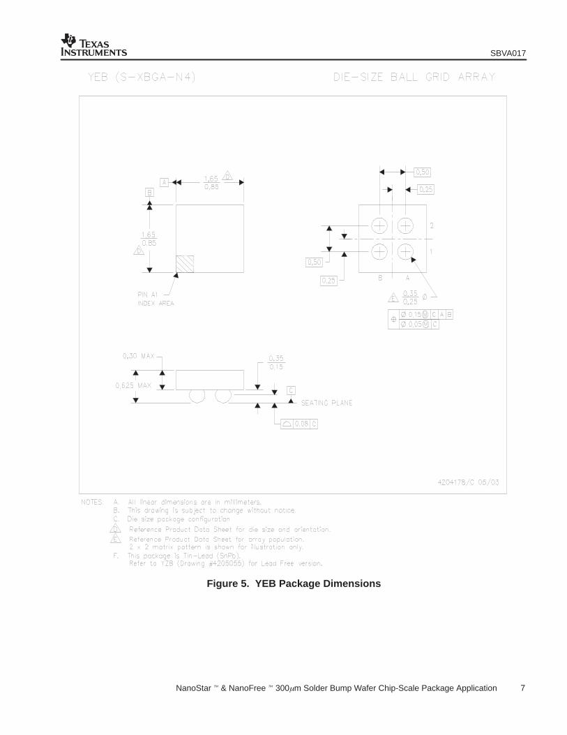
2.2 NanoStar Package Dimensions
Typical NanoStar package dimensions are shown in Figure 5. Current released package draw-ings are available through the TI web site (www.ti.com). These package drawings are generic foreach array footprint. The drawings provide details of solder bump tolerances, package thick-ness, and basic size information. Keep in mind that NanoStar is a die size package; therefore,the exact package outline varies within a given package footprint. Each device in the NanoStarpackage will detail the exact product device size in the relevant data sheet.
SBVA017
7 NanoStar & NanoFree 300m Solder Bump Wafer Chip-Scale Package Application
Figure 5. YEB Package Dimensions

SBVA017
8 NanoStar & NanoFree 300m Solder Bump Wafer Chip-Scale Package Application
2.3 Thermal Performance
Typical thermal performance of the NanoStar devices can be found in Table 2. Due to the smallsize, low profile, and location of the power plane, the primary path for heat dissipation in theNanoStar device is through the board. This makes the Theta JB a more significant number thanTheta JA when considering the thermal characteristics of a NanoStar package. (Theta JA, or JA,is junction-to-air; Theta JB, or JB, is junction-to-board). Thermal performance can be improved forall package sizes by using thermal planes in a multilayer PCB under the NanoStar device. It is notrecommended to clamp any heatsink to the top of a NanoStar device. Figure 6 shows a graphicalcomparison of the thermal resistance change across a range of package designators for a simpleJEDEC 1S0P board. Figure 7 shows the possible improvement by using a typical four-layerJEDEC 2S2P board.
The
rmal
Res
ista
nce
NanoStarTM Package Type
300
50
100
150
200
250
YE
M
YE
L
YE
K
YE
J
YE
H
YE
G
YE
F
YE
D
YE
C
YE
U
YE
B
0 m/s
1 m/s
2 m/s
3 m/s
(JA
)
Figure 6. JEDEC 1S0P Thermal Performance Data Graph
NanoStarTM Package Type
YE
M
YE
L
YE
K
YE
J
YE
H
YE
G
YE
F
YE
D
YE
C
YE
U
YE
B
The
rmal
Res
ista
nce
0 m/s
1 m/s
2 m/s
3 m/s
180
80
100
120
140
160
60
40
(JA
)
Figure 7. JEDEC 2S2P Thermal Performance Data Graph

SBVA017
9 NanoStar & NanoFree 300m Solder Bump Wafer Chip-Scale Package Application
Table 2. Simulated Thermal Resistance Data (1)
Chip Size(mm)
Linear Airflow Velocity (m/s)
(C/W) 0 m/s 1 m/s 2 m/s 3 m/s JEDEC PCB
YEB RJA 161.14 144.57 137.07 131.95 2S2P
0.85 x 0.85 RJA 304.51 229.93 202.24 186.62 1S0P
4-Bump RJB 76.54 2S2P
RJC 77.05 1S0P
YEU RJA 129.93 114.51 108.26 104.06 2S2P
0.95 x 1.25 RJA 247.84 183.41 160.92 148.31 1S0P
5-Bump RJB 51.10 2S2P
RJC 54.29 1S0P
YEC RJA 126.383 110.04 103.98 99.88 2S2P
0.85 x 1.35 RJA 257.80 185.03 160.88 147.45 1S0P
6-Bump RJB 53.26 2S2P
RJC 55.97 1S0P
YED RJA 107.58 92.58 87.42 84.02 2S2P
0.85 x 1.85 RJA 231.09 163.62 142.04 130.14 1S0P
8-Bump RJB 43.16 2S2P
RJC 39.27 1S0P
YEF RJA 105.44 91.54 86.29 82.79 2S2P
1.35 x 1.35 RJA 215.45 148.93 127.01 114.92 1S0P
9-Bump RJB 35.11 2S2P
RJC 38.49 1S0P
YEG RJA 88.99 75.31 70.55 67.43 2S2P
1.85 x 1.35 RJA 202.89 136.15 115.95 104.98 1S0P
12-Bump RJB 31.83 2S2P
RJC 26.20 1S0P
YEH RJA 75.96 66.86 62.23 59.29 2S2P
1.85 x 1.85 RJA 185.51 121.93 103.31 93.19 1S0P
16-Bump RJB 26.59 2S2P
RJC 22.75 1S0P
YEJ RJA 70.89 61.79 59.05 57.36 2S2P
1.85 x 2.35 RJA 173.48 112.28 94.55 85.08 1S0P
20-Bump RJB 20.47 2S2P
RJC 17.55 1S0P
NOTE 1: Per JESD 51−7 [4], and JESD 51−3 [5], Power = 1W

SBVA017
10 NanoStar & NanoFree 300m Solder Bump Wafer Chip-Scale Package Application
Table 2. Simulated Thermal Resistance Data (1) (continued)
JEDEC PCB3 m/s2 m/s1 m/s0 m/s(C/W)
YEK RJA 57.87 51.59 48.14 45.85 2S2P
2.35 x 2.35 RJA 162.01 105.30 90.28 80.22 1S0P
25-Bump RJB 18.86 2S2P
RJC 14.14 1S0P
YEL RJA 55.02 48.33 45.42 43.50 2S2P
2.35 x 2.85 RJA 147.42 97.49 82.42 74.33 1S0P
30-Bump RJB 17.98 2S2P
RJC 12.32 1S0P
YEM RJA 47.49 45.50 43.49 42.19 2S2P
2.85 x 2.85 RJA 141.41 90.60 74.02 65.47 1S0P
36-Bump RJB 15.26 2S2P
RJC 10.34 1S0P
NOTE 1: Per JESD 51−7 [4], and JESD 51−3 [5], Power = 1W
2.4 Board Level Reliability
The Texas Instruments packaging development team has performed extensive board-level reli-ability (BLR) testing on the NanoStar WCSP. These board-level reliability tests are in addition tostandard device performance testing. A summary of the package-level tests and the passing cri-teria for WCSP are given in Table 3.
Table 3. Board-Level Reliability Test Matrix
Test Condition Criteria Sample Size
Temperature Cycle −40 to +125°C, 1 cycle/hr, 15 min. ramp(1) 1000 cycles, R < 1.2x from R0 36
Temperature Shock −40 to +125°C, 2 cycle/hr, 5 min. ramp(2) 500 cycle minimum, R < 1.2x from R0 36
Drop 0.5m, 2000+µε(3) measured impact 10 drops, R < 1.2x from R0 5
Key Push100 cycle/min., 20N max force,1300µε(3), Displacement = 2.7mm max
20K cycles, R < 1.2x from R0 5
Three-Point Bend Strain Rate 5mm/min. 100mm span R < 1.2x from R0 (35mm maximum) 5
NOTE 1: Per JEDEC JESD22−A104B Condition G [6]NOTE 2: Per IPC-9701NOTE 3: µε = microstrain
SBVA017
11 NanoStar & NanoFree 300m Solder Bump Wafer Chip-Scale Package Application
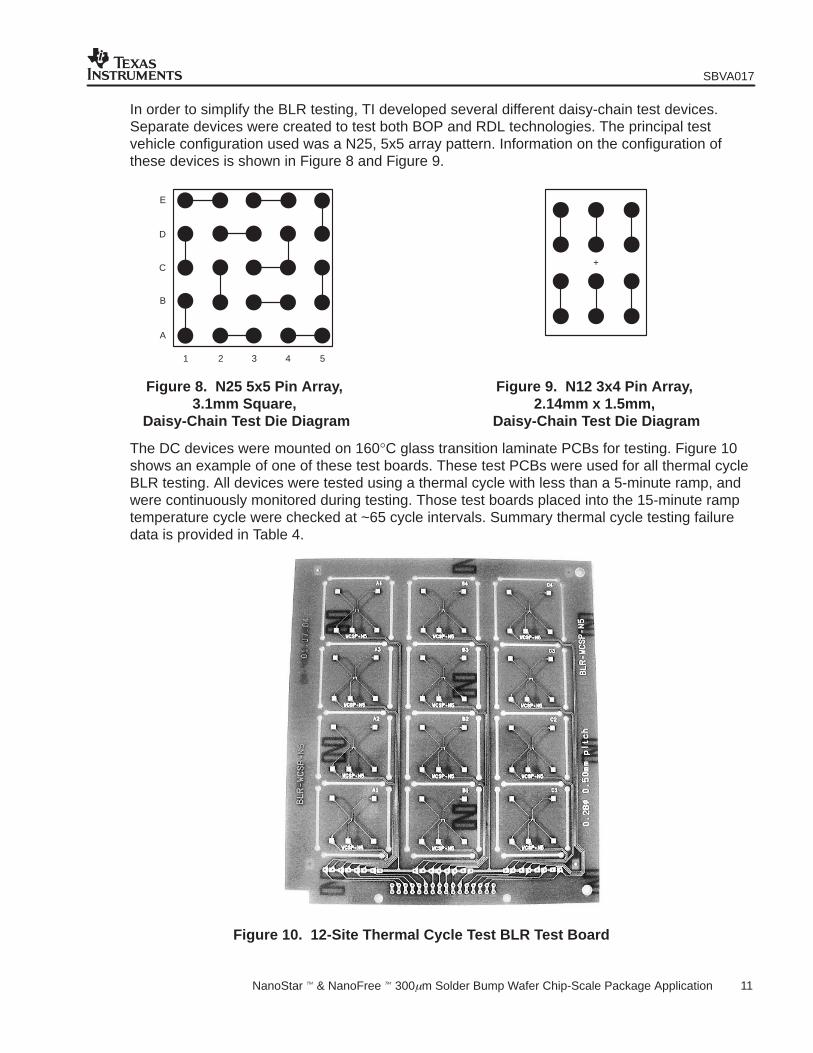
In order to simplify the BLR testing, TI developed several different daisy-chain test devices.Separate devices were created to test both BOP and RDL technologies. The principal testvehicle configuration used was a N25, 5x5 array pattern. Information on the configuration ofthese devices is shown in Figure 8 and Figure 9.
1
E
D
C
B
A
2 3 4 5
Figure 8. N25 5x5 Pin Array, 3.1mm Square,
Daisy-Chain Test Die Diagram
+
Figure 9. N12 3x4 Pin Array, 2.14mm x 1.5mm,
Daisy-Chain Test Die Diagram
The DC devices were mounted on 160°C glass transition laminate PCBs for testing. Figure 10shows an example of one of these test boards. These test PCBs were used for all thermal cycleBLR testing. All devices were tested using a thermal cycle with less than a 5-minute ramp, andwere continuously monitored during testing. Those test boards placed into the 15-minute ramptemperature cycle were checked at ~65 cycle intervals. Summary thermal cycle testing failuredata is provided in Table 4.
Figure 10. 12-Site Thermal Cycle Test BLR Test Board

SBVA017
12 NanoStar & NanoFree 300m Solder Bump Wafer Chip-Scale Package Application
Table 4. NanoStar Board Level Reliability Summary
Vehicle
Test N25 Tin-Lead N25 Lead-Free N12 Tin-Lead
1st Fail 63% WeibullLife 1st Fail 63% Weibull
Life 1st Fail 63% WeibullLife
Temperature Cycle 1660 Cycles 2502 Cycles 1389 Cycles 2301 Cycles 1827 Cycles +2579(1)
Temperature Shock 1177 Cycles 1850 Cycles 1515 Cycles 2326 Cycles 1516 Cycles 3885 Cycles
Drop 123 Drops 208 Drops 101 Drops 160 Drops 223 Drops 548 Drops
Key Push 0/8 Fail 451301 Cycles 0/8 Fail 1.24M Cycles 0/8 Fail 651160 Cycles
Three-Point Bend N/A Maximum N/A Maximum N/A Maximum
NOTE 1: Test stopped at 2579 cycles due to chamber malfunction.
The NanoStar WCSP BLR testing demonstrated excellent reliability in all testing. The BLRWeibull graph shows the difference achieved by using different thermal cycle profiles. As shownin Figure 11, the Weibull slope increased and the N63 fatigue life decreased as the thermal ramptemperature rate increased. Additionally, the graph shows significant improvement in a fatiguecycle file between brittle polymeric materials and TI’s new re-passivation polymer technology.Also, the cycle life increases as the array size on WCSP decreases. This finding is shown by theincreased performance exhibited by the N12 device.
10
100
90
80
70
60
50
40
30
20
10
0100 1k 10k
BCB
Polymide
3 Min Ramp
5 Min Ramp
15 Min Ramp
12 Bump Pkg5 Min Ramp
Figure 11. N25 TCT Weibull Comparison of Ramp Rates and Materials
Cross-sectional images of NanoStar BLR failures are shown in Figure 12 through Figure 15. Theimages display typical solder cracks for BLR failures obtained with both tin-lead and lead-freesolder.

SBVA017
13 NanoStar & NanoFree 300m Solder Bump Wafer Chip-Scale Package Application
Figure 12. Typical Tin-Lead BLR SolderFatigue Crack
Figure 13. Enlargement of Crack Area inFigure 12
Figure 14. Typical Lead-Free BLR SolderFatigue Crack
Figure 15. Enlargement of Crack Area inFigure 14
3 Printed Circuit Board Assembly
NanoStar can be assembled with normal SMT assembly practices in solder paste print,component placement, and reflow. This section provides detailed recommendations to achievebest overall performance.
3.1 PCB Design Guidelines
The size of WCSP requires care in the PCB design process for optimum reliability, processing,and manufacturability. In addition to the land pattern information (see section 3.2), the followingrules should be observed:
• Best reliability results are achieved when the PCB laminate glass transition temperature isabove the operating range of the intended application.

SBVA017
14 NanoStar & NanoFree 300m Solder Bump Wafer Chip-Scale Package Application
• For PCBs using a Ni/Au surface finish, the gold thickness should be less 0.5µm to avoid areduction in solder joint thermal fatigue performance.
• Ni/Au surface finishes are not recommended for use with lead-free solder devices. OSPsurface finish will deliver superior reliability results.
• Trace routing away from WCSP device should be balanced in x and y directions to avoidunintentional component movement as a result of unbalanced solder wetting forces. (Anexample of this effect can be seen in Figure 16.)
• Solder-mask thickness should be less than 1 mil (.001in) on top of the copper circuit pattern.
• Circuit traces routed away from PCB land pads should be less than 100µm wide (preferably≈ 75µm) in the exposed area inside the solder mask opening. Wider trace widths will reducedevice stand-off and impact reliability.
• Recommended solder paste is Type 3.
Figure 16. Example of 5x5 Array Balanced Routing Pattern
3.2 PCB Land Pattern Recommendations
The recommended land pattern for all NanoStar solder pads is a Non-Solder-Mask defined(NMSD) solder pad. The size and shape recommendation for all devices is identical, and isgiven in Figure 17. Recommended dimensions are provided in Table 5.
Table 5. Recommended PCB Solder Land Pattern
Solder Pad Definition Copper Pad Solder Mask Opening Copper Thickness
Non-Solder-Mask Defined (NMSD) 275µm (+0.0, −25µm) 375µm (+0.0, −25µm) 1oz max (32µm)

SBVA017
15 NanoStar & NanoFree 300m Solder Bump Wafer Chip-Scale Package Application
Figure 17. Recommended Solder Land Pattern Outline
3.3 Solder Paste Stencil Design
Stencil design for NanoStar should follow standard industry recommendations such as IPC-7525Stencil Design Guidelines [7]. Best BLR performance is achieved when maximum devicestandoff exists, which is obtained with maximum manufacturable solder paste volume. Thesolder stencil opening is identical for all solder pads in a WCSP array. Recommended stencilinformation is found in Table 6.
Table 6. Recommended Solder Stencil Pattern
Stencil Opening (1) Stencil Thickness (2)
300µm Round, or 275µm x 275µm Square 100−125µm thick
NOTE 1: Round stencil opening preferred.NOTE 2: Best solder stencil performance will be achieved using laser cut stencils with electro-polishing. The
use of chemically etched stencils results in inferior solder paste volume control.
3.4 Component Placement
Typical surface mount placement equipment capable of placing similar sized SMT devices canassemble the NanoStar WCSP. The package provides robust self-alignment, and will re-centerwith up to 150µm of displacement. There is one recommendation concerning placement forcefor best successwith component placement processes, however.
• On equipment without component force adjustments, the Z placement height should be setto avoid overdriving the board location. Optimally, the Z height should be set at one-half theprinted solder paste height.

SBVA017
16 NanoStar & NanoFree 300m Solder Bump Wafer Chip-Scale Package Application
• On equipment with component placement force adjustments, the maximum recommendedplacement force is 35g/bump. Exceeding this force level can reduce reliability due toexcessive silicon impact stress and subsequent damage.
3.5 Reflow
Recommended solder reflow profiles for NanoStar are shown in Figure 18. Critical reflowtemperatures are given in Table 7.
183
165
135
Time
Tem
pera
ture
(C
)
Min. 60 sec.Max. 120 sec.
Min. 30 sec.Max. 90 sec.
Max. 235C, Min. 195C
SnPb Eutectic (AT−Alloy and S2062)Recommended Temperature Profile
Data courtesy of Senju Metal Industry Co.
220
180
150
Time
Tem
pera
ture
(C
)
Min. 60 sec.Max. 120 sec.
Min. 30 sec.Max. 90 sec.
Max. 260C, Min. 230C
Pb−Free Bump NanoFree Recommended Temperature Profile
Figure 18. Recommended Reflow Profiles

SBVA017
17 NanoStar & NanoFree 300m Solder Bump Wafer Chip-Scale Package Application
Table 7. Recommended Critical Reflow Parameters
Process Step Tin-Lead Solder Lead-Free Solder
Ramp Rate 3°C/sec Maximum 3°C/sec
Pre-Heat 165°C, 60 to 120 seconds Max. 150°C to 180°C, 60 to 180 seconds
Time above Liquidus 183°C, 30 to 90 seconds 220°C, 30 to 90 seconds
Peak Temperature 235°C 255°C ±5°C
Time within 5°C of Peak Temperature 10 to 20 seconds 10 to 20 seconds
Ramp Down Rate 6°C/sec Maximum 6°C/sec Maximum
4 Tape and Reel Information
4.1 Material Specifications
TI offers tape-and-reel packing for NanoStar packages in standard packing quantities (SPQ) of250 and 3000 units/reel. The units are shipped in embossed carrier tape, sealed with heat-acti-vated or pressure-sensitive cover tape, and wound on plastic reels. All of the tape-and-reel ma-terials comply with EIA−481, and EIA−541 [8, 9]. The EIA specifications are shown in Figure 19and Figure 20, as well as in Table 8 and Table 9. The carrier tape is made of conductive polysty-rene and has a surface resistivity that falls within the static-dissipative range (1×10⁵ to1×1011Ω2). Heat-activated or pressure-sensitive, antistatic, clear polyester film is used for thecover tape. The dimensions of most interest to the end user are tape width (W), cavity pitch (P),and cavity size (A0, B0, K0), as shown in Figure 19. Due to the wide range of die sizes within agiven array size, the cavity size dimensions will vary. Please refer to the specific product datasheet for devices of interest for the cavity dimensions (A0, B0, K0).
The units are placed in the carrier-tape cavity, with pin 1 located as specified in EIA−481. Thelongest axis of the package is perpendicular to the tape sprocket holes, and pin 1 is closest tothe round sprocket holes. Thus, for rectangular or square packages, pin 1 is located in quad-rant 1 (see Figure 21). All dimensions are in millimeters.
+
+ + + + + +
+ + + + + +
8
CL
0.25 ± 0.05¯1.55± 0.05
1.75 ± 0.10
Y
Y
Pin 1(1)
Section Y − Y Dimensions in mm
P1
P0 E1
B0F
W
A0
P2
NOTE: (1) Pin 1 location isin the upper left−hand cornerof the cavity. Units are shippedwith bumps down.
K0
Figure 19. Pocket Tape Dimensions

SBVA017
18 NanoStar & NanoFree 300m Solder Bump Wafer Chip-Scale Package Application
Table 8. Common Tape Dimensions by Designator (1)
Designator YEB YEC YED YEF YEG YEH YEJ YEK YEL YEM
Pocket Pitch, P1 4.00 ± .10 4.00 ± .10 4.00 ± .10 4.00 ± .10 4.00 ± .10 4.00 ± .10 8.00 ± .10 8.00 ± .10 8.00 ± .10 8.00 ± .10
Sprocket Hole-to-PocketCenterline, F 3.50 ± .05 3.50 ± .05 3.50 ± .05 3.50 ± .05 3.50 ± .05 3.50 ± .05 5.50 ± .05 5.50 ± .05 5.50 ± .05 5.50 ± .05
Sprocket Hole-to-PocketOffset, P2
2.00 ± .05 2.00 ± .05 2.00 ± .05 2.00 ± .05 2.00 ± .05 2.00 ± .05 2.00 ± .05 2.00 ± .05 2.00 ± .05 2.00 ± .05
Sprocket Hole Pitch, P0 4.00 ± .10 4.00 ± .10 4.00 ± .10 4.00 ± .10 4.00 ± .10 4.00 ± .10 4.00 ± .10 4.00 ± .10 4.00 ± .10 4.00 ± .10
Tape Width, W 8 8 8 8 8 8 12 12 12 12
Reel Diameter, Max. 178 178 178 178 178 178 178 / 330 178 / 330 178 / 330 178 / 330
NOTE 1: All dimensions are in mm.
A
D(1)
D(1)
W1 (measured at hub)
W2 (measured at hub)
W3 (includes flangedistortion at outer edge)
Full Radius
CArbor Hole Diameter
N(hub diameter)
If present, tape slotin core for tape start:2.5mm min width x10.0mm min depth
Access Hole at Slot Location(∅49mm min)
NOTE 1: All dimensions are in mm.
Figure 20. Pocket Tape Dimensions
Table 9. Reel Specifications (1)
ReelDiameter
(A)
ReelWidth(W1)
HubDiameter Max
(N)
ReelThickness
(W2)
Arbor-HoleDiameter
(C)Quantity/Reel
178 ± 0.60 8.4 ± 1.65 62 ± 0.50 14.4 ± 1.65 13.0 ± 0.5/−0.2 250 or 3000
178 ± 0.60 12.4 ± 1.65 62 ± 0.50 18.4 ± 1.65 13.0 ± 0.5/−0.2 250
330 ± 0.60 12.4 ± 1.65 62 ± 0.50 18.4 ± 1.65 13.0 ± 0.5/−0.2 3000
NOTE 1: All dimensions are in mm.

SBVA017
19 NanoStar & NanoFree 300m Solder Bump Wafer Chip-Scale Package Application
Quadrant
SquarePackage
1 2 1 2
3 4
3 4
Figure 21. Carrier-Tape Cavity Quadrant Location for Pin 1, per EIA−481B
5 SymbolizationThe top of the package is laser-marked with device name, date code, assembly-site code,assembly-lot trace code, and pin-1 location as space allows. Table 10 shows the device-markingsymbolization guidelines for NanoStar packages.
The Character and WCSP Laser Mark Image column entries in Table 10 have the followingmeanings:
CCCC Device name (shortened in accordance with product data sheet)
Y Year
M Month
D Day
S Site code
LLLL Lot trace code
A Pin-1 quadrant identifier (data sheet specifies exact pin-1 location)
Tin-lead solder devices use a “1” (one), and lead-free solder devices use a “0” (zero).
For specific marking information on a particular device, please see the device data sheet (avail-able for download from the TI web site).
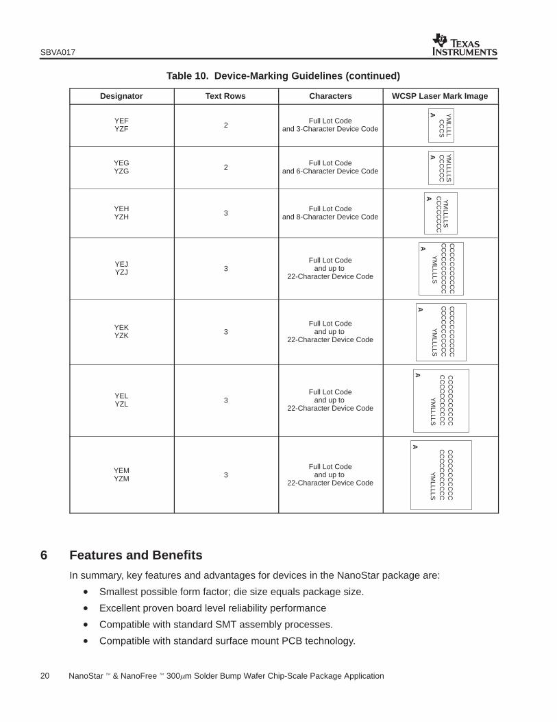
Table 10. Device-Marking Guidelines
Designator Text Rows Characters WCSP Laser Mark Image
YEBYZB4YZT
1Lot Code
and 2-Character Device Code
YM
DS
CC
A
YEA/YZAYEP/YZT
5YZT/6YZTYEC/YZCYEQ/YZQYEU/YZU
1Lot Code
and 2-Character Device Code
YM
DC
CS
A
YEDYZD 0
Full Lot CodeNo Device Code
YM
LLLLSA
SBVA017
20 NanoStar & NanoFree 300m Solder Bump Wafer Chip-Scale Package Application
Table 10. Device-Marking Guidelines (continued)
Designator WCSP Laser Mark ImageCharactersText Rows
YEFYZF 2
Full Lot Codeand 3-Character Device Code
YM
LLLL
AC
CC
S
YEGYZG 2
Full Lot Codeand 6-Character Device Code
YM
LLLLS
A CC
CC
CC
YEHYZH 3
Full Lot Codeand 8-Character Device Code
YM
LLLLS
A CC
CC
CC
CC
YEJYZJ 3
Full Lot Codeand up to
22-Character Device Code
YM
LLLLS
A CC
CC
CC
CC
CC
CC
CC
CC
CC
CC
CC
YEKYZK 3
Full Lot Codeand up to
22-Character Device Code
YM
LLLLS
A CC
CC
CC
CC
CC
CC
CC
CC
CC
CC
CC
YELYZL 3
Full Lot Codeand up to
22-Character Device Code
YM
LLLLS
A CC
CC
CC
CC
CC
CC
CC
CC
CC
CC
CC
YEMYZM 3
Full Lot Codeand up to
22-Character Device Code
YM
LLLLS
A
CC
CC
CC
CC
CC
CC
CC
CC
CC
CC
CC
6 Features and Benefits
In summary, key features and advantages for devices in the NanoStar package are:
• Smallest possible form factor; die size equals package size.
• Excellent proven board level reliability performance
• Compatible with standard SMT assembly processes.
• Compatible with standard surface mount PCB technology.

SBVA017
21 NanoStar & NanoFree 300m Solder Bump Wafer Chip-Scale Package Application
7 Conclusion
Texas Instruments NanoStar package offerings are bare die packages, with improved perfor-mance and reduced package footprint over similar SOT-23, SC-70, and SOIC packages. Addi-tionally, the NanoStar packages meet the industry’s lead-free demands, have reliable solderabil-ity using either lead or lead-free solder paste, and can be reworked and manufactured usingconventional equipment. The packages allow for product miniaturization and comply with dimen-sional specifications of JEDEC standard MO−211.
Acknowledgments
The author wishes to thank the entire NanoStar development team. This package would nothave been possible without the support of each and every person on the worldwide WCSPteam. Unfortunately, the list of contributors is too large for print.
References
Listed JEDEC references can be found at: http://www.jedec.org/download/default.cfm.
1. Package standard MO−211, Die−size Ball Grid Array, Fine Pitch, Thin/Very,Thin/Extremely, Thin Profile, F−XBGA. (JEDEC)
2. Smetana, J. Wafer Scale CSP Reliability Characterization Project Final Report. HighDensity Packaging User Group International.Scottsdale, AZ and Alvsjo, Sweden. Availableat: http://www.hdpug.org/public/4−papers/2001/ws−csp/wafer_scale_final.pdf.
3. Package standard MO−211, Die−size Ball Grid Array, Fine Pitch, Thin/Very,Thin/Extremely, Thin Profile, F−XBGA. (JEDEC)
4. High Effective Thermal Conductivity Test Board for Leaded Surface Mount Packages. JESD 51−7. (JEDEC)
5. Low Effective Thermal Conductivity Test Board for Leaded Surface Mount Package.JESD 51−3 (JEDEC)
6. Test Method – Temperature Cycling. JESD22−A104B. (JEDEC)
7. Stencil Design Guidelines. IPC−7525. Available at: www.dynamixtechnology.com/docs/IPC−7525s.pdf, or order from IPC (www.ipc.org).
8. Taping of Surface Mount Components for Automatic Placement. EIA−481. ElectronicsIndustry Alliance. Available at: http://www.chipro.com/PDF%20Files/EIA−481−B.pdf, ororder from EIA (www.eia.org).
9. Packing Material Standards for ESD Sensitive Items. EIA−541. Available for purchase at:http://www.tiaonline.org/standards/search_results2.cfm?document_no=EIA%2D541, orfrom EIA (www.eia.org).

IMPORTANT NOTICE
Texas Instruments Incorporated and its subsidiaries (TI) reserve the right to make corrections, modifications,enhancements, improvements, and other changes to its products and services at any time and to discontinueany product or service without notice. Customers should obtain the latest relevant information before placingorders and should verify that such information is current and complete. All products are sold subject to TI’s termsand conditions of sale supplied at the time of order acknowledgment.
TI warrants performance of its hardware products to the specifications applicable at the time of sale inaccordance with TI’s standard warranty. Testing and other quality control techniques are used to the extent TIdeems necessary to support this warranty. Except where mandated by government requirements, testing of allparameters of each product is not necessarily performed.
TI assumes no liability for applications assistance or customer product design. Customers are responsible fortheir products and applications using TI components. To minimize the risks associated with customer productsand applications, customers should provide adequate design and operating safeguards.
TI does not warrant or represent that any license, either express or implied, is granted under any TI patent right,copyright, mask work right, or other TI intellectual property right relating to any combination, machine, or processin which TI products or services are used. Information published by TI regarding third-party products or servicesdoes not constitute a license from TI to use such products or services or a warranty or endorsement thereof.Use of such information may require a license from a third party under the patents or other intellectual propertyof the third party, or a license from TI under the patents or other intellectual property of TI.
Reproduction of information in TI data books or data sheets is permissible only if reproduction is withoutalteration and is accompanied by all associated warranties, conditions, limitations, and notices. Reproductionof this information with alteration is an unfair and deceptive business practice. TI is not responsible or liable forsuch altered documentation.
Resale of TI products or services with statements different from or beyond the parameters stated by TI for thatproduct or service voids all express and any implied warranties for the associated TI product or service andis an unfair and deceptive business practice. TI is not responsible or liable for any such statements.
Following are URLs where you can obtain information on other Texas Instruments products and applicationsolutions:
Products Applications
Amplifiers amplifier.ti.com Audio www.ti.com/audio
Data Converters dataconverter.ti.com Automotive www.ti.com/automotive
DSP dsp.ti.com Broadband www.ti.com/broadband
Interface interface.ti.com Digital Control www.ti.com/digitalcontrol
Logic logic.ti.com Military www.ti.com/military
Power Mgmt power.ti.com Optical Networking www.ti.com/opticalnetwork
Microcontrollers microcontroller.ti.com Security www.ti.com/security
Telephony www.ti.com/telephony
Video & Imaging www.ti.com/video
Wireless www.ti.com/wireless
Mailing Address: Texas Instruments
Post Office Box 655303 Dallas, Texas 75265
Copyright 2004, Texas Instruments Incorporated