Introduction to Chemistry – Background for Nanoscience and Nanotechnology Prof. Petr Vanysek.

Nanoscience and –technology in Physics and Chemistry (Curator Hans-Jürgen Butt)
At a glance:
Nanoscience is the science of objects with typical sizes of 1-100 nm. If matter is di-
vided into such small objects the mechanical, electric, optical, and magnetic proper-
ties can change. Interfaces rather then bulk properties dominate. Quantum effects
due to the size limitation come into play. Nanoscience and Nanotechnology are inter-
disciplinary, crossing boundaries between physics, chemistry, chemical, electric and
mechanical engineering.
Nanoscience, that is the science of objects with typical sizes of 1-100 nm, is one of
the most important developments in the last decades. Miniaturization of electronic
devices to sizes of the elementary units below 1 µm has revolutionized our daily live.
New technologies were required to enter the nanoscale because many of the tradi-
tional techniques do not work at the nanoscale. The relation between nanoscience
and technology is like a symbiosis. Scientific discoveries lead to new technologies.
The technology enables new fundamental insights. Two new technologies which en-
abled the progress of nanoscience are scanning tunneling and scanning force mi-
croscopy. They allow to image and manipulate objects on surfaces with sufficient
precision even in ambient conditions or in liquids.
Most properties of solids are altered when their dimensions approach the nanoscale.
As an example, consider a particle of 1x1x1 nm3. This contains roughly 43 = 64 at-
oms. Only 8 atoms of them are in the interior, while 87% of the atoms are at the sur-
face. The electronic, magnetic, chemical, and mechanical properties of nanoparticles
are therefore dominated by surface atoms. Simply by finely dispersing ordinary bulk
materials new properties can be created: inert materials become catalysts, insulators
become conductors, or stable materials become combustible. A rather inert material
like Au may for example become an efficient and selective catalyst when of the size
of a few nm.
The characteristic length scale of a system can often be given intuitively. For exam-
ple, for a spherical particle one would use the diameter, for a thin film the thickness.
For more complex systems intuition can, however, lead to ambiguous results. We

2
suggest to us the ratio of the total volume V divided by the total interfacial area A of a
system as the characteristic length scale: λ = V/A. Nanoscience is thus the science of
systems with λ in the range of 1 to 100 nm.
The most simple nanomaterials are particles dispersed in a medium. Although
nanoparticles have been made since the time of Michael Faraday and colloid science
has particularly flourished in the 1920ies and 30ies, making functional nanoparticles is
and will remain a challenge. On one side we can consider atomically defined
nanoparticles. Proteins made by living cells are one example. The largest syntheti-
cally made nanosized macromolecule with an atomically defined structure are the
dendrimers.
Figure K. Müllen, MPI Polymer Research
Making organic nanoparticles with specific functions and properties is and will remain
a challenge. Organic functional nanoparticles and their dispersions find wide-spread
applications ranging from coatings, flocculation and colorization to biolabeling, drug
delivery and gene transfection 1. The critical issues in their preparation are size, size
distribution and stability in the prevailing environment. Although methods of emulsion
polymerization are well established for the preparation of polymer latices, the chemi-
cal functionalization of such particles continues to be a challenge.
The interaction of nanoparticles with cells is an important issue 2. It is important be-
cause on one hand nanoparticles are potential drug carriers. On the other hand, pos-
sible health risks have to be excluded.
For many applications inorganic nanoparticles are used rather than organic ones.
Inorganic materials can be mechanically more stable and they are more resilient to
high temperature.
Example M. Antonietti, MPI Colloid and Interface Science
Methods to make such particles are developed and improved with respect to making
more complex structures in a more efficient way.
Example K. Sundmacher, MPI Magdeburg
Example: F. Schüth, MPI Coal Research
A closely related field is that of nanocomposites where inorganic particles, after suit-
able compatibilization, are used to improve the mechanical, electrical and optical
properties of organic polymers. Since nanoparticles are smaller than the wavelength
3
of light they are invisible (unless the molecules absorb light). Surface functionalized
nanoparticles of UV-absorbing zinc oxide are prepared by inverse mini-emulsion us-
ing amphiphilic copolymers as stabilizers.
One reason for the success of composite materials is that embedded particles can
significantly improve the mechanical properties of the matrix. This can be achieved
by mixing the second component into the first one. Raabe achieved a similar effect
by a self-organized precipitation effect in a metal alloy leading to a steel with im-
proved strength.
Example: D. Raabe, MPI Iron Research
Nanomaterials are characterized by a large interfacial area. Such materials are for
example desirable as a substrate for catalysts or in filters. Therefore nanoporous ma-
terials with a defined pore size distribution are continued to be developed. Often or-
ganic substances are used as a template for inorganic materials. The reason is that
the formation of defined nanostructures in organic molecules such a surfactants or
block copolymers is well understood and can be adjusted.
One driving force for nanoscience and –technology was the desire to miniaturize
electric circuits and storage media. Over the past decades, the MOSFET, one stan-
dard transistor, has continually been scaled down in size; modern integrated circuits
incorporate MOSFETs with feature sizes down to 32 nm. At the same time the size to
store one bit of information has decreased to 200 GB/sqinch leading to bit sizes of 56
nm.
Example G. Schütz, MPI Metal Research
A characteristic feature of the nano-world is that quantum effects can occur. If a clas-
sical bicycle rider arrives at a hill he has no choice other than to convert chemical
energy in his muscles into potential energy, which he may partly gain back as kinetic
energy once the top of the hill is reached. Otherwise he will not get across the bar-
rier. A quantum mechanical particle, e.g. an electron, has more options: for a finite
hill size there is always a chance of arriving at the other side at the same energy. To
some extent the hill is transparent, albeit with perhaps a very small probability. This
“tunnel effect” is at the heart of the scanning tunneling microscope (STM).
Example: J. Kirschner, MPI Microstructure Physics
Example K. von Klitzing, MPI Solid State Research

4
One might ask: Why is it useful to shrink electronic circuits and storage media in
size? One reason is that integrated circuits also become faster and consume less
energy. Storage devices with a high density can be faster accessible. This is a con-
tinuing motivation to go from micro- to nano-electronics.
A similar motivation drives scientist to integrate and miniaturize chemistry and to try
to understand and manipulate smaller and smaller amounts of liquids. This is essen-
tial when only small amounts of reactants are available. It also helps to better control
potentially toxic or explosive reactions. The idea is to integrate a complete laboratory
into a silicon waver or a plastic chip. Although this concept has not penetrated our
everyday live to the same extent as microelectronics has, the first commercial appli-
cations are meanwhile available, e.g., enzymatic analysis and DNA-sequencing. The
channels in which the substances are transported in existing devices have typical
diameters of 50-100 µm and are still macroscopic. Correspondingly this technique is
called microfluidics. From the physicists point of view there is no qualitative differ-
ence between such a microfluidic device and a conventional macroscopic setup. The
flow in the channel is described by the same hydrodynamic equations. The only dif-
ference is that in general there is no turbulence in microfluidic channels such that
reactants only mix slowly by diffusion. This presents a technological problem but not
a conceptual one.
In contrast, further miniaturization towards the nanometer scale -leading to nano-
fluidic systems - is both a technical and a scientific challenge. The behaviour on the
nanoscale is qualitatively different from the micron scale due to the influence of ther-
mal fluctuations, the long range of intermolecular interactions, the influence of chan-
nel walls on the fluid, and finally the finite size of the molecules which matter in nano-
fluidic systems. Understanding and manipulating small amounts of liquids is thus a
long term challenge.
Example: S. Dietrich, MPI Metals Research
Example: H.-J. Butt, MPI Polymer Research
From the fundamental point of view, nanoscience connects two traditional fields of
science. The structure and properties of single molecules are relatively well under-
stood. For example, spectroscopic and theoretical methods are well developed so
that the energy levels can be measured and directly be compared to calculations. On
5
the other end, continuum solid state physics and chemistry know how to deal with of
infinitely extended materials. The transition region is much less understood.
Example: H.-J. Freund, Fritz-Haber-Institute
While large amounts of a material can be described independently on what is around
them, small amounts are often dominated by the boundary condition. For example,
when a liquid material is filled into nanopores, it might change its properties and be-
come ordered and rigid. If the same liquid is kept as an isolated drop in air it remains
fluid.
To make nanostructures two different approaches can be used: the lithographic con-
struction of single features (top down) and the spontaneous self-assembly of small
objects to larger architectures (bottom up). Both have advantages and disadvan-
tages. In many applications, both will be applied to create a desired structure. In this
respect supramolecular chemistry has a particularly important role. Supramolecular
chemistry aims to organize molecular building blocks by means of noncovalent inter-
actions into complex arrangements.
Example: Kern, MPI Solid State Research
Such a combination of approaches will also be necessary to further progress in the
field of organic or more specifically polymer electronics. Organic electronics, that is
the fabrication of electronic and optoelectronic devices, using organic light emitting
and charge transporting materials3, 4, will continue to be a key challenge for science
and technology and holds a tremendous market potential. While device efficiency
and stability stand in the foreground of application oriented work, there are still many
fundamental issues regarding the behavior of excitons and charge carriers at or close
to interfaces and the supramolecular packing of the organic molecules.
Example: Kremer, MPI Polymer Research
Future directions:
• Better ways of producing nanoscale objects and of organizing them to com-
plex arrangements. This includes the development of appropriate processing
methods for arranging materials on the nanoscale.
6
• Interfacing nanoobjects to the outside world, e.g. by electrically connecting
them.
• Make new composite materials by deliberately utilizing internal interfaces.
• Understanding and manipulating the flow of liquids on the nanoscale.
• Develop new methods to characterize the structure and properties (e.g. elec-
tric conductivity, dielectric permittivity, magnetic susceptibility, heat conductiv-
ity and capacity, mechanical deformability, refractive index) of nano-objects in
different environments non-destructively and fast.
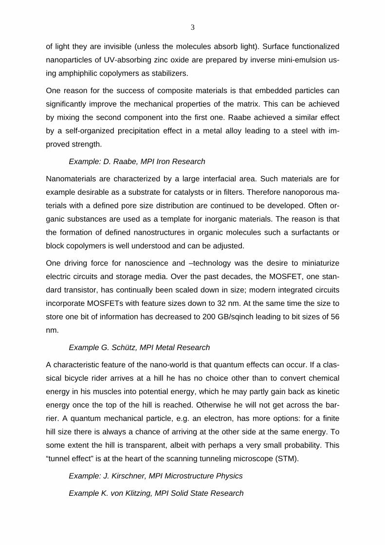
K. Müllen. Dendrimers
A dendrimer is a synthetic, three-dimensional macromolecule. It is built up from a
monomer, with new branches added in steps until a tree-like structure is created
(dendrimer comes from the Greek dendra, meaning tree). The largest molecules ever
made with an atomically defined structure is the dendrimer shown in the figure 5. It
consists of precisely 5592 benzene rings and has a molecular mass of 546404 g/mol.
Dendrimers can not only be made large. They can also be made with specific func-
tions, such as efficient fluorophores 6 or as carriers, e.g. for drugs 7. The inner part of
the dendrimer provides a defined environment, while the groups on the surface regu-
late the compatibility with the environment.
7
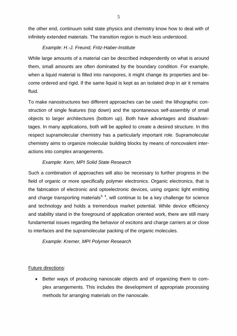
M. Antonietti. Synthesis of nanoparticles
Many materials, which are relevant for novel energy cycles and more efficient chemi-
cal reactions (catalysis) do not exist as nanostructures so that “de novo” systems
have to be designed from scratch. This for instance holds for metal carbide and ni-
tride particles, which offer new pathways for metal/base catalysis. They also hold the
record in mechanical hardness and magnetization. In general, both size and shape
add to the favourable properties and must be controlled or adjusted. New cathode
nanomaterials for the lithium battery are another target for novel nanostructures
where progress will directly impact society 8.
Figure: TiN nanoparticles imaged by transmission electron microscopy.

8
K. Sundmacher, Nanoparticles by design: Using emulsion droplets as nanore-actors for precipitation
Taylor-made nanoparticles with well defined size and shape are needed for new ap-
plications e.g. in surface physics, catalysis, and biomedicine. Emulsion-assisted pre-
cipitation is a very attractive process technology for the production of taylor-made
nanoparticles 9. In this approach, the droplets of microemulsions (droplet size 2 to
100 nm) or miniemulsions (droplet size > 100 nm and < 1 µm) are used as reaction
compartments to perform the precipitation of nanoparticles, initiated by a liquid-phase
chemical reaction which is followed by nucleation and growth of solid particles.
Figure: Barium sulphate nanoparticles made by microemulsion precipitation.
9
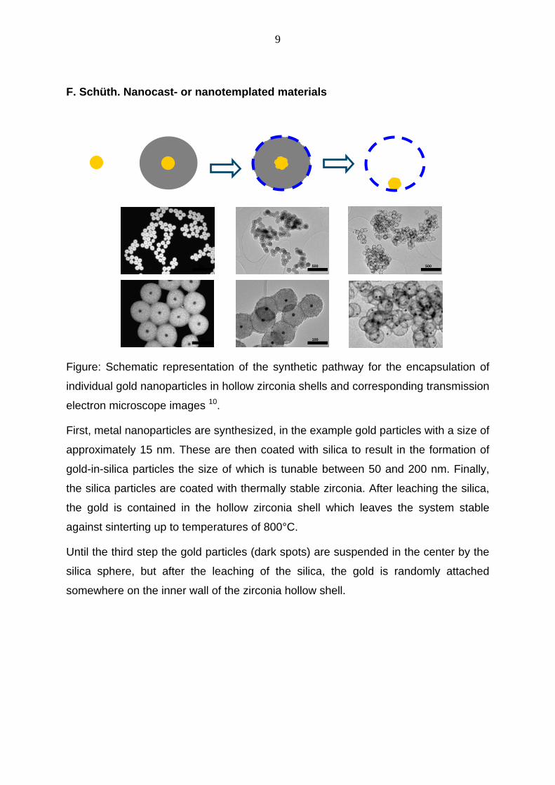
F. Schüth. Nanocast- or nanotemplated materials
Gold clus- Au@SiO2 core- Au@SiO2@ZrO2 sys- Au, @ZrO2 sys-tem
500
100
500
100
500
Figure: Schematic representation of the synthetic pathway for the encapsulation of
individual gold nanoparticles in hollow zirconia shells and corresponding transmission
electron microscope images 10.
First, metal nanoparticles are synthesized, in the example gold particles with a size of
approximately 15 nm. These are then coated with silica to result in the formation of
gold-in-silica particles the size of which is tunable between 50 and 200 nm. Finally,
the silica particles are coated with thermally stable zirconia. After leaching the silica,
the gold is contained in the hollow zirconia shell which leaves the system stable
against sinterting up to temperatures of 800°C.
Until the third step the gold particles (dark spots) are suspended in the center by the
silica sphere, but after the leaching of the silica, the gold is randomly attached
somewhere on the inner wall of the zirconia hollow shell.

10
D. Raabe, Self-organized nano-precipitates in ultrahigh strength steels
Steels with a ultrahigh strength above 1 GPa and good ductility above are of para-
mount relevance for lightweight engineering design strategies and corresponding
CO2 savings. Raabe et al. developed a new concept for precipitation hardened duc-
tile high strength martensitic and austenitic-martensitic steels with even up to 1.5
GPa strength. The alloys are characterized by a low carbon content (0.01 wt.% C)
and 9-15 wt.% Mn to obtain different levels of austenite stability, and minor additions
of Ni, Ti, and Mo (1-2 wt.%). The latter elements are required for creating nano-
precipitates during aging heat treatment 11, 12.
Figure: Atom probe tomography measurements conducted on a maraging TRIP alloy
with 12 wt.% Mn. Atomic distribution of the Ni content in the form of nano-clusters
(green). The shaded zones indicate atomic Ni concentrations above 20 at.%. Al
(blue), Mn (red).

11
G. Schütz. Magnetic vortices
Magnetic thin-film square-or disc-shaped nanostructures with nanometer dimensions
exhibit a magnetic vortex state: the magnetization vectors lie in the film plane and
curl around the structure centre. At the centre of the vortex, a small, stable core ex-
ists where the magnetization points either up or down.
The reversal of the vortex core via excitation of the vortex gyration mode was discov-
ered by time-resolved X-ray microscopy 13. This discovery of an easy core reversal
mechanism did not only open the possibility of using such systems as magnetic
memories, but also initiated the fundamental investigation of the core switching
mechanism itself. They may pave the way to an alternative magnetic date storage
technology.
Figure: Three dimensional representation of the experimentally observed magnetic
vortex core profile 14.
12
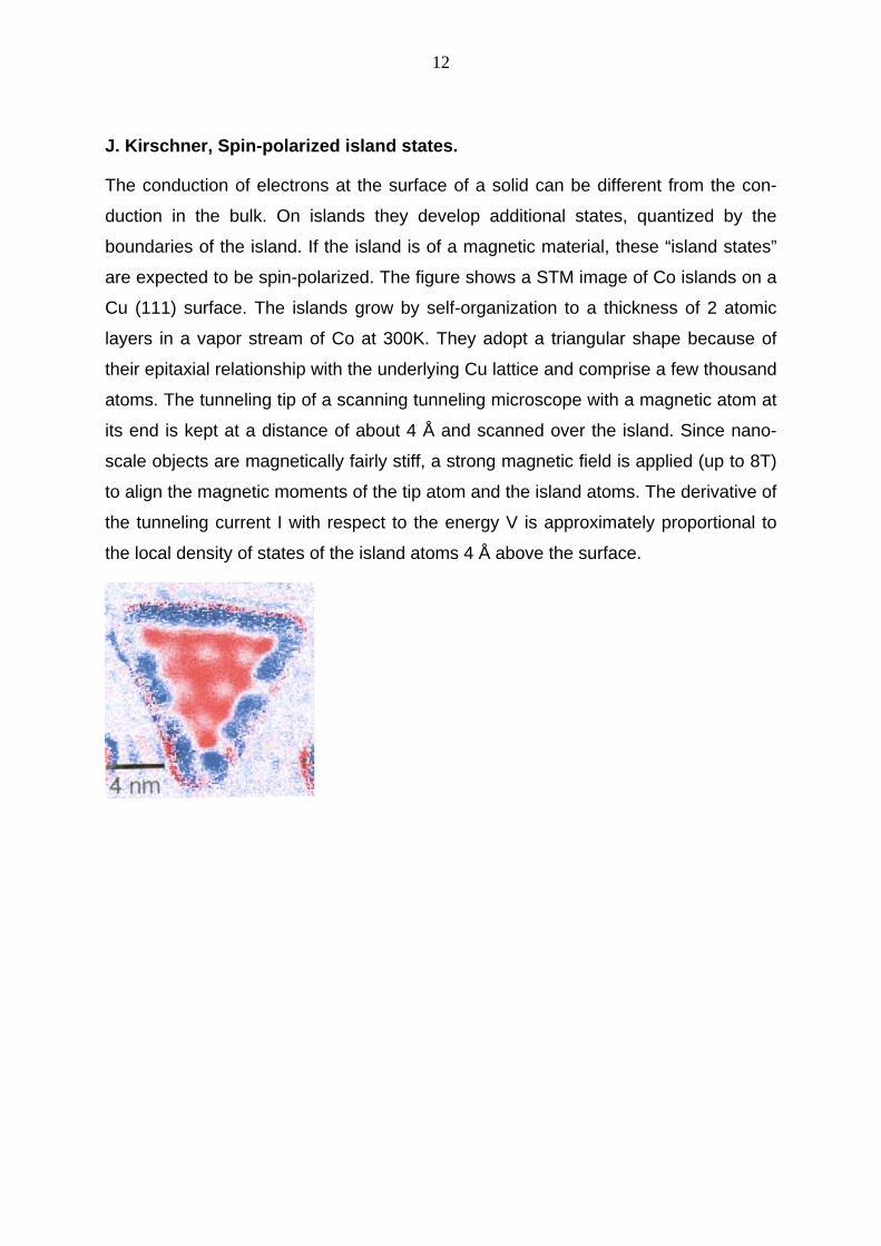
J. Kirschner, Spin-polarized island states.
The conduction of electrons at the surface of a solid can be different from the con-
duction in the bulk. On islands they develop additional states, quantized by the
boundaries of the island. If the island is of a magnetic material, these “island states”
are expected to be spin-polarized. The figure shows a STM image of Co islands on a
Cu (111) surface. The islands grow by self-organization to a thickness of 2 atomic
layers in a vapor stream of Co at 300K. They adopt a triangular shape because of
their epitaxial relationship with the underlying Cu lattice and comprise a few thousand
atoms. The tunneling tip of a scanning tunneling microscope with a magnetic atom at
its end is kept at a distance of about 4 Å and scanned over the island. Since nano-
scale objects are magnetically fairly stiff, a strong magnetic field is applied (up to 8T)
to align the magnetic moments of the tip atom and the island atoms. The derivative of
the tunneling current I with respect to the energy V is approximately proportional to
the local density of states of the island atoms 4 Å above the surface.

13
K. von Klitzing. Quantum effects in Nanoelectronics: Counting single electrons
From the development of the first transistor in 1947, great interest has been directed
towards the technological development of semiconducting devices and the investiga-
tion of their physical properties. A very vital field within this topic focuses on the elec-
trical transport through low-dimensional structures, where the quantum confinement
of charge carriers leads to the observation of a variety of phenomena. In the aim of
reaching even smaller sized and more compact devices, semiconductor Indium Ar-
senide nanowires grown via Molecular Beam Epitaxy technique are processed add-
ing source and drain contacts and several types of electrostatically coupled gates 15.
The flexibility in tailoring the chemistry of nanowires will most likely make them the
building blocks of nanosized devices.
Figure: Scanning electron microscope image of the molecular-beam-epitaxy grown
Indium Arsenide nanowire with electrostatically coupled lateral gates.

14
S. Dietrich. Theory of liquid flow in chemical channels.
Differences between the wettability of various substrates can be used to guide non-
volatile fluids on surfaces (first figure). Different techniques to fabricate thin wettable
stripes (so-called chemical channels) on otherwise non-wettable substrates are
available. On these chemical channels fluids can be guided between chemical walls
formed by the non-wettability of the embedding substrate 16-18.
Figure: Cross-section of a homogeneously filled chemical “channel” in a molecular
dynamics simulation. The green and red dots are the wetting and non-wetting sub-
strate atoms, respectively. The fluid molecules are short chain flexible polymers
(blue) collect in a circular area which has a contact angle Θ with the substrate.

15
H.J Butt. Capillary force between nanorods
Using porous alumina 19 as a template, arrays of polymer nanorods can be grown.
Porous alumina contains a hexagonal array of nanosized pores. It is placed on a
substrate, for example a gold surface. The nanosized pores are used as reaction
containers to form the polymer rods. Afterwards the alumina is etched away, leaving
the polymer rods standing on the gold. When exposing the rods to moisture the bun-
dles were formed caused by capillary forces. For nanosized structures surface ten-
sion forces can easily dominate.
Figure: Polycyanurate nanorod arrays 20 grown on top of gold after exposure to mois-
ture. Size: 3.5 × 2.5 µm2.
16
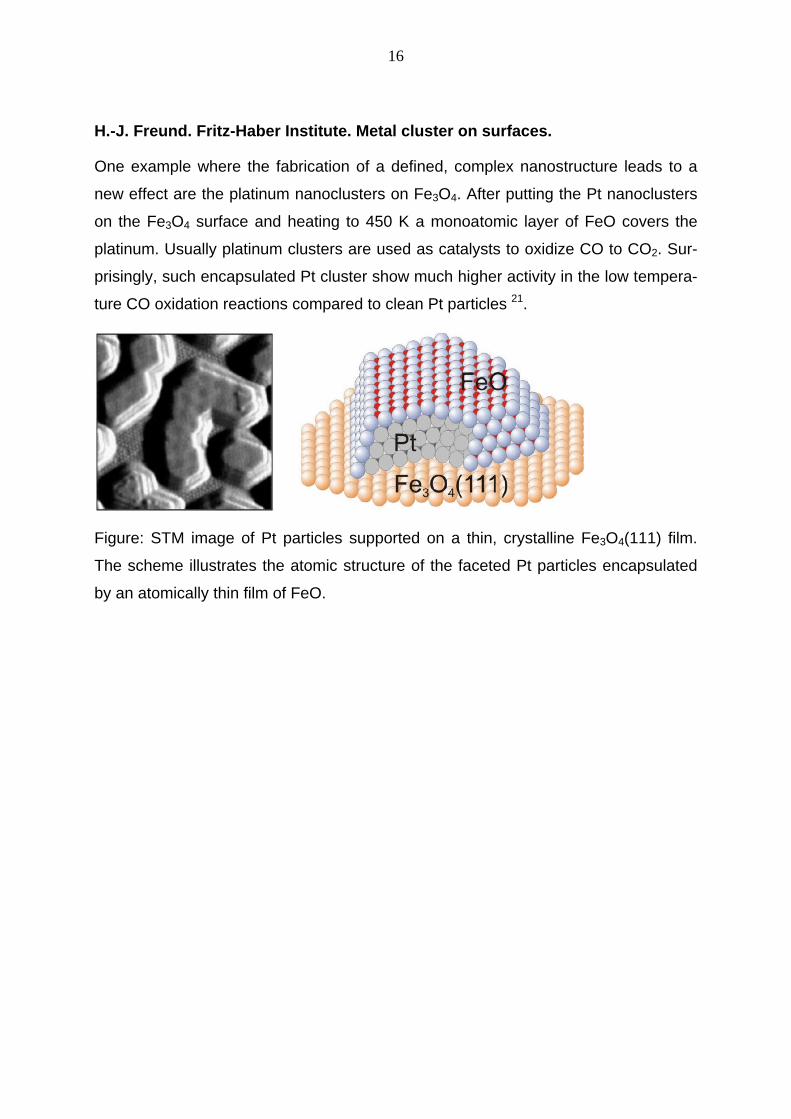
H.-J. Freund. Fritz-Haber Institute. Metal cluster on surfaces.
One example where the fabrication of a defined, complex nanostructure leads to a
new effect are the platinum nanoclusters on Fe3O4. After putting the Pt nanoclusters
on the Fe3O4 surface and heating to 450 K a monoatomic layer of FeO covers the
platinum. Usually platinum clusters are used as catalysts to oxidize CO to CO2. Sur-
prisingly, such encapsulated Pt cluster show much higher activity in the low tempera-
ture CO oxidation reactions compared to clean Pt particles 21.
Figure: STM image of Pt particles supported on a thin, crystalline Fe3O4(111) film.
The scheme illustrates the atomic structure of the faceted Pt particles encapsulated
by an atomically thin film of FeO.

17
K. Kern. Bottom-up nano-fabrication.
The archetype of a thermodynamically driven structure formation is bio-inspired mo-
lecular self-assembly. This refers to the spontaneous association of molecules under
near-equilibrium conditions into stable, well-defined aggregates joined by noncova-
lent bonds. It is the key building principle of all living matter and the basics of supra-
molecular chemistry. To make full use of this approach in nanotechnology, noncova-
lent intermolecular interactions have to be mastered and manipulated in a controlled
way. The construction of nanostructures molecule-by-molecule introduces the distinct
advantage that organization and functionality can be manipulated by chemical de-
sign.
Figure: Example, where a chiral Kagomé lattice has been self-assembled on a silver
surface from simple ditopic molecular bricks 22.

18
K. Kremer. Design of self-organized materials for organic electronics.
Conjugated polymers and cyclic π-systems have been studied for almost a decade in
order to develop various optoelectronic devices, such as light-emitting diodes, field
effect transistors, optically pumped lasers, and organic solar cells. The quintessence
of organic materials stems from the possibility to control their properties using syn-
thetic methods. Electronic structure, self-organization abilities, stability, ease of proc-
essing – all these properties can be adjusted by choosing a suitable chemical struc-
ture of a material. Development of the parameter-free simulation methods can help to
formulate structure-property-processing relationships and hence assist rational de-
sign of organic semiconductors.
Figure. Structure of polyaromatic hydrocarbons as derived from simulations and con-
firmed by X-ray diffraction results for which the charge carrier mobility was simulated 23.

19
1. Klapper, M., Clark, C. G. & Müllen, K. Application-directed syntheses of sur-face-functionalized organic and inorganic nanoparticles. Polymer International 57, 181-202 (2008).
2. Mailander, V. & Landfester, K. Interaction of Nanoparticles with Cells. Biomac-romolecules 10, 2379-2400 (2009).
3. Li, C. et al. Perylenes as sensitizers in hybrid solar cells: how molecular size influences performance. J. Materials Chemistry 19, 5405-5415 (2009).
4. Wu, J. S., Pisula, W. & Müllen, K. Graphenes as potential material for elec-tronics. Chemical Reviews 107, 718-747 (2007).
5. Clark, C. G. et al. Controlled MegaDalton assembly with locally stiff but glob-ally flexible polyphenylene dendrimers. J. Am. Chem. Soc. 129, 3292-3301 (2007).
6. Oesterling, I. & Mullen, K. Multichromophoric polyphenylene dendrimers: To-ward brilliant light emitters with an increased number of fluorophores. J. Am. Chem. Soc. 129, 4595-4605 (2007).
7. Bauer, R. E., Clark, C. G. & Müllen, K. Precision host-guest chemistry of poly-phenylene dendrimers. New J. Chemistry 31, 1275-1282 (2007).
8. Hu, Y. S. et al. Synthesis of hierarchically porous carbon monoliths with highly ordered microstructure and their application in rechargeable lithium batteries with high-rate capability. Adv. Functional Materials 17, 1873-1878 (2007).
9. Niemann, B., Veit, P. & Sundmacher, K. Nanoparticle precipitation in reverse microemulsions: Particle formation dynamics and tailoring of particle size dis-tributions. Langmuir 24, 4320-4328 (2008).
10. Arnal, P. M., Comotti, M. & Schuth, F. High-temperature-stable catalysts by hollow sphere encapsulation. Angewandte Chemie Intern. Ed. 45, 8224-8227 (2006).
11. Raabe, D., Ponge, D., Dmitrieva, O. & Sander, B. Designing Ultrahigh Strength Steels with Good Ductility by Combining Transformation Induced Plasticity and Martensite Aging. Adv. Engineering Materials 11, 547-555 (2009).
12. Raabe, D., Ponge, D., Dmitrieva, O. & Sander, B. Nanoprecipitate-hardened 1.5 GPa steels with unexpected high ductility. Scripta Materialia 60, 1141-1144 (2009).
13. Van Waeyenberge, B. et al. Magnetic vortex core reversal by excitation with short bursts of an alternating field. Nature 444, 461-464 (2006).
14. Vansteenkiste, A. et al. X-ray imaging of the dynamic magnetic vortex core deformation. Nature Physics 5, 332-334 (2009).
15. Jabeen, F., Rubini, S. & Martelli, F. Growth of III-V semiconductor nanowires by molecular beam epitaxy. Microelectronics Journal 40, 442-445 (2009).
16. Rauscher, M., Dietrich, S. & Koplik, J. Shear flow pumping in open micro- and nanofluidic systems. Phys. Rev. Lett. 98, 224504 (2007).
17. Koplik, J., Lo, T. S., Rauscher, M. & Dietrich, S. Pearling instability of nano-scale fluid flow confined to a chemical channel. Phys. Fluids 18, 032104 (2006).
20
18. Mechkov, S. et al. Contact line stability of ridges and drops. Europhys. Lett. 80 (2007).
19. Steinhart, M., Wehrspohn, R. B., Gösele, U. & Wendorff, J. H. Nanotubes by template wetting: A modular assembly system. Angewandte Chemie-Inter. Ed. 43, 1334-1344 (2004).
20. Yameen, B. et al. Polycyanurate thermoset networks with high thermal, me-chanical, and hydrolytic stability based on liquid multifunctional cyanate ester monomers with bisphenol A and AF units. Macromol. Chemistry Physics 209, 1673-1685 (2008).
21. Sun, Y. N. et al. Monolayer iron oxide film on platinum promotes low tempera-ture CO oxidation. J. Catalysis 266, 359-368 (2009).
22. Schlickum, U. et al. Chiral kagome lattice from simple ditopic molecular bricks. J. Am. Chem. Soc. 130, 11778-11782 (2008).
23. Feng, X. L. et al. Towards high charge-carrier mobilities by rational design of the shape and periphery of discotics. Nature Materials 8, 421-426 (2009).