
Nanoparticle Enhanced Thin Film Solar Cells - WFUusers.wfu.edu/ucerkb/Nan242/L16-Solar_Cells.pdf ·...
16
Nanoparticle Enhanced Thin Film Solar Cells
Transcript of Nanoparticle Enhanced Thin Film Solar Cells - WFUusers.wfu.edu/ucerkb/Nan242/L16-Solar_Cells.pdf ·...

Nanoparticle Enhanced Thin Film Solar Cells

Solar Cells
• Solar cells convert visible light to electricity.
• It is one of the “clean” sources of energy.• In theory a 100 square mile area covered
with solar panels would be sufficient for the energy needs of the US.
• Solar cells are based on the photovoltaic effect.
Photovoltaic Effect
• Discovered in 1839 as a light induced current between two metal electrodes.
• When photons are absorbed in a material, some electrons gain enough energy to become free and contribute to current.
• If the light is incident on a p-n junction, the absorbed photon creates an electron-hole pair.
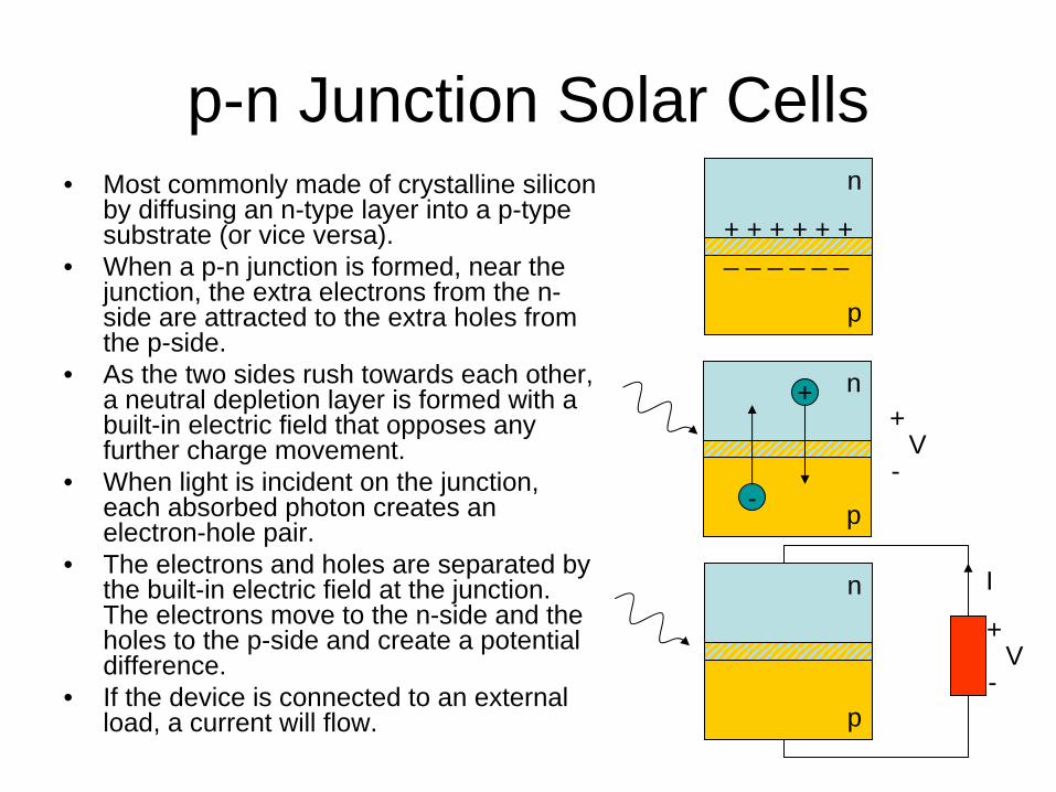
p-n Junction Solar Cells• Most commonly made of crystalline silicon
by diffusing an n-type layer into a p-type substrate (or vice versa).
• When a p-n junction is formed, near the junction, the extra electrons from the n- side are attracted to the extra holes from the p-side.
• As the two sides rush towards each other, a neutral depletion layer is formed with a built-in electric field that opposes any further charge movement.
• When light is incident on the junction, each absorbed photon creates an electron-hole pair.
• The electrons and holes are separated by the built-in electric field at the junction. The electrons move to the n-side and the holes to the p-side and create a potential difference.
• If the device is connected to an external load, a current will flow.
+ + + + + +_ _ _ _ _ _
n
p
n
p-
+
n
p
I
V-
+
V-
+

Current – Voltage Characteristics
mmm VIP =Since the solar cell is essentially a diode, it has the I-V characteristics of one
I
VIm
Vm
RL
hν
IL RL
IS
V
I
Overall solar cell efficiency:c
m
EAP
=η ,where E is solar irradiance in W/m2
under standard conditions and Ac is the surface area of the solar cell in m2.

Efficiency in p-n Junction Cells • Practical efficiencies
are around 15%.• Solar cell efficiency is
affected by many factors:– Reflectance of the
surface– Band gap of the cell
material vs. incident photon energy
– Collection efficiency of free electrons
– Internal device resistance
Si bandgap
Typical c-Si Solar Cell Structure

Comparison of Efficiencies

Thin Film Solar Cells• While many technical
difficulties with crystalline cells can be overcome or mitigated, cost is still a major factor.
• Thin film solar cells can be cheaper to manufacture.
• The main materials used in thin film solar cells are amorphous Silicon, CdTe and CIS/CGIS.
• Thicknesses are ~1 micron.• Efficiencies are < 10%.

Enhanced Light Scattering with Nanoparticles
• One issue with thin film cells is the reduced absorption of sunlight due to the small thickness of the film.
• One group in Australia (ANU) is using silver nanoparticles to enhance absorption. (Opt. Exp. 16, 21793 (2008)
• A thin (~100nm) film of silver is deposited on the oxidized surface of a thin silicon film solar cell by vacuum evaporation.
• Subsequent heating at 200 °C creates silver nanoparticles through bubbling.
• The silver nanoparticles can scatter visible light very efficiently and create a trapped mode for the incident light.
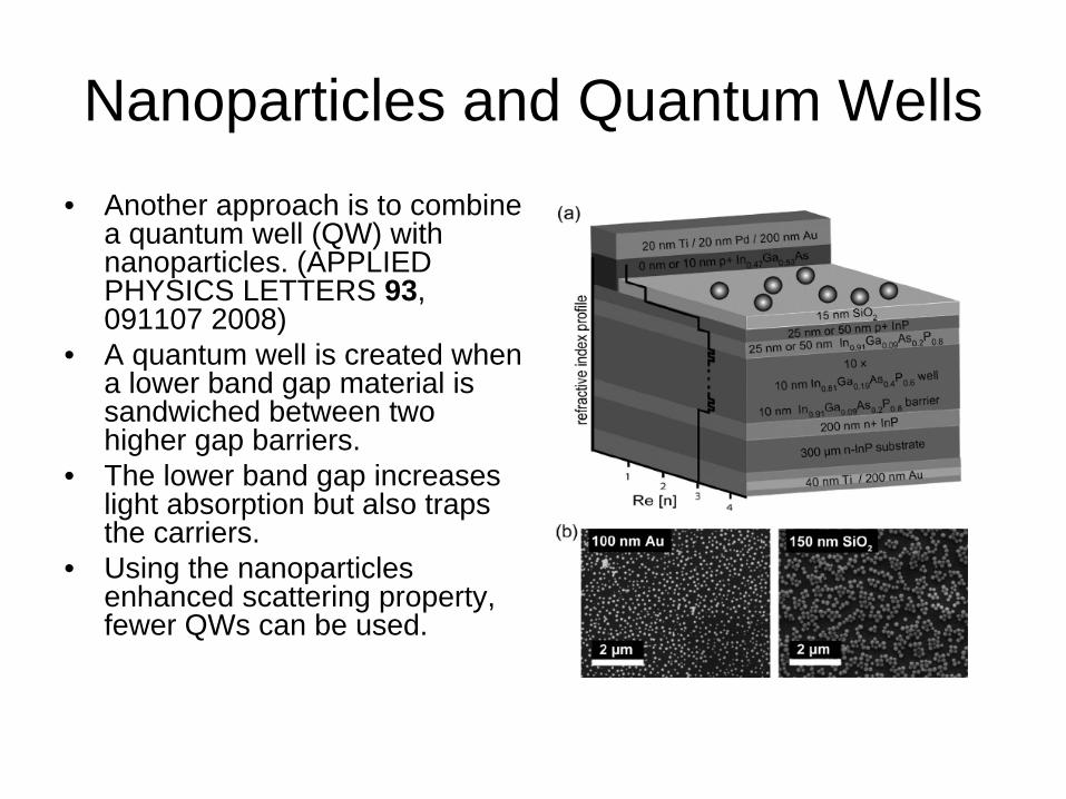
Nanoparticles and Quantum Wells• Another approach is to combine
a quantum well (QW) with nanoparticles. (APPLIED PHYSICS LETTERS 93, 091107 2008)
• A quantum well is created when a lower band gap material is sandwiched between two higher gap barriers.
• The lower band gap increases light absorption but also traps the carriers.
• Using the nanoparticles enhanced scattering property, fewer QWs can be used.
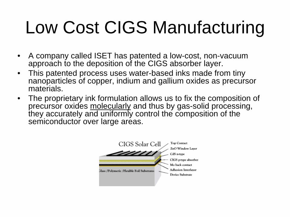
Low Cost CIGS Manufacturing• A company called ISET has patented a low-cost, non-vacuum
approach to the deposition of the CIGS absorber layer.• This patented process uses water-based inks made from tiny
nanoparticles of copper, indium and gallium oxides as precursor materials.
• The proprietary ink formulation allows us to fix the composition of precursor oxides molecularly and thus by gas-solid processing, they accurately and uniformly control the composition of the semiconductor over large areas.

Dye Sensitized Solar Cells• A photon is absorbed by
the dye and excites an electron in the dye.
• The electron is then “injected” into the wires or particles.
• Travels to the electrode, which is connected to an external circuit.
• The dye is regenerated by the electrolyte.
Enhanced Light Absorption with Nanoparticles
• Because c-Si has a band gap in the NIR, most of the energy of the visible and UV photons are wasted as heat when the photon is absorbed.
• Depositing thin layers with different band gaps will improve efficiency but increase cost.
• Creating nanocrystalline layers of porous silicon is a convenient way of achieving this goal.
• When crystals are confined to nanometer size, the band gap of the material becomes wider.
• Porous silicon can be created by electrochemical etching of a c-Si surface and produce ~2 nm size particles with band gaps in the visible or near UV. (IEEE Photonics Technology Letters 16, 1927-1929 (2004))

Organic Photovoltaics• Unlike p-n junction devices, solar cells made out of
organic molecules are made out of electron donor and acceptor materials.
• When an electron-hole pair is created in a polymer chain, it is strongly bound.
• In order to create a current, this pair has to be dissociated. The acceptor material is for this purpose.

Enhancing Organics PVs with Nanoparticles
• Nanoparticles can be more efficient as acceptors.
• The process, called charge transfer, can increase efficiency.
• WFU Nanotech is very active in this area.

Another Polymer Example• Using an aluminum oxide template
consisting of nanometer sized honeycomb array the polymer P3HT is drawn through the openings through vacuum and capillary forces.
• The structure is then backfilled with C60 which acts as the electron acceptor.
• The aluminum oxide allows the P3HT chains to align themselves in a stacked array which increases conductivity.
• The honeycomb structure increases the surface area which helps with electron transfer.
• While reported efficencies are low (~1 %) the method is cheap and scalable.
• Ref: Adv. Funct. Mater. 2010, 20, 540– 545.


![[PPT]PowerPoint Presentation - WFUusers.wfu.edu/natalie/f13phy113/lecturenote/Lecture17.pptx · Web view10/24/2013 PHY 113 C Fall 2013 -- Lecture 17 Webassign questions – Assignment](https://static.fdocuments.in/doc/165x107/5acd81337f8b9ab10a8dbec9/pptpowerpoint-presentation-view10242013-phy-113-c-fall-2013-lecture-17.jpg)


