


Nanomaterials and their Optical Applications - iap.uni … · Type of organic compound = conjugates...
67
http://www.iap.uni-jena.de/multiphoton Nanomaterials and their Optical Applications Winter Semester 2013 Lecture 06 [email protected]
Transcript of Nanomaterials and their Optical Applications - iap.uni … · Type of organic compound = conjugates...
[email protected] Lecture 06 http://www.iap.uni-jena.de/multiphoton
Nanomaterials and their Optical Applications Winter Semester 2013
Lecture 06

[email protected] Lecture 06
Outline: Organic nanomaterials for optics 2
1. Organic quantum-confined structure
a. Nanomers
b. Organic quantum dots
2. Carbon nanotubes
3. Graphene the first fully extensible organic light emitting diode (OLED) that can stretch up to 45% and are still functional. The use of carbon nanotubes impregnated with a liquid polymer, have managed to create a smooth, elastic and transparent electrode, which can emit light in
Intrinsically Stretchable Polymer Light-Emitting Devices Using Carbon Nanotube-Polymer Composite Electrodes, Advanced Materials, 2011

[email protected] Lecture 06
Organic nanomaterials: introduction 3
Difference between organic & inorganic compounds ?
1. Organic compounds are produced by living things. Inorganic compounds are
produced by non-living natural processes or by human intervention in the
laboratory.
2. Inorganic compounds can form salts. Organic compounds can't.
3. Organic compounds contain carbon. Inorganic compounds don't.
4. Organic compounds contain carbon-hydrogen bonds. Inorganic compounds
don't.
5. Inorganic compounds contain metal atoms. Organic compounds don't.
6. An organic compound is whatever an organic chemist says it is; an inorganic
compound is whatever an inorganic chemist says it is.

[email protected] Lecture 06
Organic nanomaterials: introduction 4
Delocalized π electrons Benzene
= free electrons in semiconductors Type of organic compound = conjugates molecules or polymers 2 types of bonds: σ bond = single covalent bond between 2 atoms, axial overlap of atomic orbitals π bond = double/triple bond, lateral overlap of the diretional p-type atomic orbital
Prasad, Nanophotonics, §4.7, p.115
π electrons = loosely bound electrons spread over th entire conjugated structure

[email protected] Lecture 06
Organic nanomaterials: nanomers 5
Prasad, Nanophotonics, §4.7, p.115
Monomeric unit Large size oligomers = nanomers Thus organic analog to nanowires
Analogy with conduction and valence band for molecules
HOMO = highest occupied molecular orbital = valence band LUMO = lowest unoccupied molecular orbital = conduction band
• π Bonding Molecular orbital • π * Anti-bonding molecular orbital • The pair of bonding electrons is in π • The higher the conjugation, the lower the π energy, the smaller the gap
Linear conjugated structures

[email protected] Lecture 06
Organic nanomaterials : organic quantum dots 6
Scheme of solid-state polymerization in a diacetylene crystal
nm nm
Absorption spectra of polydiacetylenes nanocrystals with different crystal sizes
H. Nakanishi, Tohoku University

[email protected] Lecture 06
Organic nanomaterials: nanomers 7
… for different length of nanomers
Prasad, Nanophotonics, §4.7, p.115
Research to develop organic and polymeric light-emitting diodes for high brightness and flexible displays

[email protected] Lecture 06
Organic nanomaterials: nanomers 8
Why organic materials ? Research to develop organic and polymeric light-emitting diodes for high brightness and flexible displays • Known to have extremely high
fluorescence quantum efficiencies in the visible spectrum, even in the blue
• Ideally suited for multicolor display
Why difficult ? • High voltage (100 V) needed to inject
charges in the organic layer Solutions ?
• Double layer of organic compound by vapor deposition
• 2.5 V bias voltage needed only

[email protected] Lecture 06
Outline: Organic nanomaterials for optics 11
1. Organic quantum-confined structure
a. Nanomers
b. Organic quantum dots
2. Carbon nanotubes
3. Graphene

[email protected] Lecture 06
Pre-history of carbon nanotubes 12
Until the mid-1980’s pure solid carbon was thought to exist in only two physical forms
and
Chemically identical
But:
Diamond is the hardest mineral
ever and graphite is very soft
Weak bonding forces (van der Waals forces) hold the sheets together
The four valence electrons of each carbon atom participate in the formation of very strong covalent bonds
diamond graphite
[email protected] Lecture 06
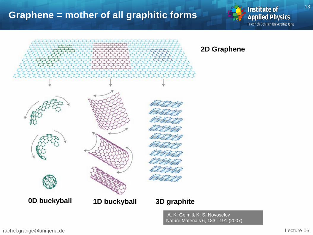
Graphene = mother of all graphitic forms 13
2D Graphene
0D buckyball 1D buckyball 3D graphite
A. K. Geim & K. S. Novoselov Nature Materials 6, 183 - 191 (2007)
[email protected] Lecture 06
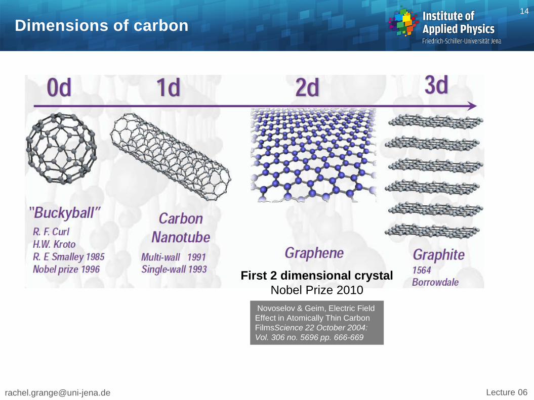
Dimensions of carbon 14
Novoselov & Geim, Electric Field Effect in Atomically Thin Carbon FilmsScience 22 October 2004: Vol. 306 no. 5696 pp. 666-669
First 2 dimensional crystal Nobel Prize 2010

[email protected] Lecture 06
Pre-history of carbon nanotubes: the fullerenes
15
They vaporized a sample of graphite with an intense pulse of laser light and used a stream of helium gas to carry the vaporized carbon into a mass spectrometer. The mass spectrum showed peaks corresponding to clusters of carbon atoms, with a particularly strong peak corresponding to molecules composed of 60 carbon atoms, C60
32 faces, 12 were pentagons and 20 were hexagons exactly like a soccer ball
Named after Buckminster Fuller, an architect, who was responsible for the design of the first geodomes in 1967

[email protected] Lecture 06
First 11 years of carbon nanotubes 17
Part of the following slides inspired by Anna Swan’s talk, Boston University
[email protected] Lecture 06
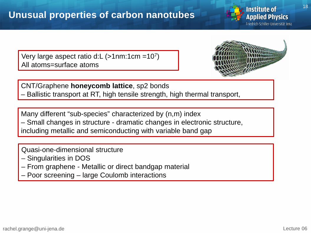
Unusual properties of carbon nanotubes 18
Very large aspect ratio d:L (>1nm:1cm =107) All atoms=surface atoms
CNT/Graphene honeycomb lattice, sp2 bonds – Ballistic transport at RT, high tensile strength, high thermal transport,
Many different “sub-species” characterized by (n,m) index – Small changes in structure - dramatic changes in electronic structure, including metallic and semiconducting with variable band gap
Quasi-one-dimensional structure – Singularities in DOS – From graphene - Metallic or direct bandgap material – Poor screening – large Coulomb interactions

[email protected] Lecture 06
Honey comb lattice 19
2 atoms/unit cell
Nomenclature • Chiral vectors (n,m) • Chiral angle θ • Chiral index ν(n-m) mod 3
CNT/Graphene honeycomb lattice, sp2 bonds – Ballistic transport at RT, high tensile strength, high thermal transport,

[email protected] Lecture 06
Honey comb lattice 20
Chiral vector (n, m)
𝑑 = (𝑛2+𝑚2 + 𝑛𝑚)1/2 0.0783 nm
Diameter

[email protected] Lecture 06
3 geometries of CNT 21
Armchair Zig-zag Chiral
The Industrial Physicist 2004 B. Weisman
The folding of the sheet controls the electronic properties of the nanotubes

[email protected] Lecture 06
Electronic Properties of CNTs 22
• Graphite (tight binding approximation) – σ bonds in-plane between the atoms – π bonds oriented out of plane to plane: weak van-der-Waals interaction between planes
• kz along tube axis is continuous • k⊥ is quantized
Brillouin zone

[email protected] Lecture 06
Electronic Properties of CNTs 23
• σ (sigma) bonds too far away from Fermi level, not important for electronic properties • π (pi) bonds are close to the Fermi level, important for electronic properties (σ -bonds ignored)

[email protected] Lecture 06
Electronic Properties of CNTs 24
Origin of metallic vs semiconducting nanotubes with varying band gap Chiral index ν (family) ν=(n-m) mod 3 ν=0 metallic ν=1,2 semiconducting
Tight binding model

[email protected] Lecture 06
Electronic Properties of CNTs 26
Model so far: graphite with modified boundary condition BUT Curvature effects: • Rolling of graphite sheet reduces interatomic distance and angles • π and σ states mix into hybrids with partly sp2 and sp3 character
Trigonal warping: Cone around K point not symmetric Excitonic effects

[email protected] Lecture 06
Electronic Properties of CNTs Beyond the single particle model
27
Science 26 July 2002: Vol. 297 no. 5581 pp. 593-596
individual fullerene nanotube in a cylindrical SDS micelle
2002: two very important experiments • Band-gap luminescence first observed
– Ratio-problem and blue-shift
• Coulomb interactions – excitons

[email protected] Lecture 06
Electronic Properties of CNTs Beyond the single particle model
28
2002: two very important experiments • Band-gap luminescence first observed
– Ratio-problem and blue-shift
• Coulomb interactions – excitons
Science 26 July 2002: Vol. 297 no. 5581 pp. 593-596
The top trace D is typical of tubes prepared in suspension without centrifugation.
Trace C is from individual SDS micelle coated nanotubes after addition of PVP. Traces B and A are from samples of individual nanotubes separated and solubilized by SDS micelles.
Blue shifted trace for single nanotubes

[email protected] Lecture 06
Electronic Properties of CNTs Beyond the single particle
29
Photoluminescence optical resonances higher energy than expected
O’Connell et al Science, (2002)
Absorption and luminescence from CNT in solution differ from calculations; blue-shift and “ratio problem” Bachilo et al, Science 2002

[email protected] Lecture 06
Electronic Properties of CNTs Discrepancy with the tight binding model
30
Excitons

[email protected] Lecture 06
Electronic Properties of CNTs In reduced dimensions
31
– Decreased electronic screening, larger binding energies – Enhanced Coulomb interactions
Exciton optical absorption in 3D,2D and 1D
1D exciton binding energies are enhanced compared 3 and 2D, but All the oscillator strength is transferred to exciton from the van Hove singularities (vHS). Unless we really know where the vHS is, it is hard to tell the difference

[email protected] Lecture 06
Carbon nanotubes : Optical properties 32
An exciton consists of a photo-excited electron and a hole bound to each other by a Coulomb interaction in a semiconducting material.
Common semiconductor: binding energy on the order of ∼10 meV carbon nanotubes : 100s meV to 1eV in Exciton levels by optical absorption is usually observed only at low temperatures
Exciton levels essential to understand: • Optical absorption, • Photoluminescence (PL) • Resonance Raman • Spectroscopy
http://blog.disorderedmatter.eu/2008/04/15/polaron-polaron-pair-exciton-exciplex/

[email protected] Lecture 06
Carbon nanotubes properties 33
Mechanical properties: (1nm to 100s nm) – Light weight, sustains extremely high tension force; 130 GPa compared to steel at <5 GPa – Highly flexible, even under low temperature. Applications: AFM tips, super-strong fabrics, polymer composites and space elevator
Space elevator
100 times stronger than steel
AFM tip

[email protected] Lecture 06
Carbon nanotubes properties 34
Transport properties High thermal conductivities w/o electrical conductivity, Semiconducting or metallic tubes, – High current density (1000X Cu). Applications: • field emission devices => field emission flat panel. • single molecular transistors

[email protected] Lecture 06
Carbon nanotubes properties 35
Functionalization of the surfaces Applications: chemical sensors, precise drug delivery, super-electric batteries and hydrogen storage
Optical properties: luminescence Applications: single molecule light emitters

[email protected] Lecture 06
Carbon nanotubes : Optical properties 36
Carbon nanotube = direct bandgap -> can generate or detect light
By changing the applied voltage:
• transistor • light detector • light emitter
Luminescence properties: Radiative and non radiative decay
nature photonics | VOL 2 | JUNE 2008 |

[email protected] Lecture 06
Carbon nanotubes : Optical properties 37
How can an electric field modify the absorption spectrum of CNT ?
• Moldulation of the absorption coefficient • Increase the spectral weight of the band to band absorption • Shift the absorption peak energies (Stark shift) • Dissociate the bound exciton
Nonlinear optics as saturable absorber:
100
95
90
85
80
75
Tran
smis
sion
(%)
200015001000500Wavelength (nm)
M1S2 S1
1.0
0.8
0.6
0.4
0.2
0.0Nor
m. t
ime
resp
onse
6420-2Time delay (ps)
1/e recoverytime: 700 fs
1.0
0.8
0.6
0.4
0.2
0.0Nor
m. t
ime
resp
onse
1.0
0.8
0.6
0.4
0.2
0.0Nor
m. t
ime
resp
onse
6420-2Time delay (ps)
1/e recoverytime: 700 fs
(a) (b) (c)
Figure 12: Single wall carbon nanotubes absorbers (SWCNT). (a) AFM image of spray deposited SWCNT on top of a Bragg reflector, (b) transmission spectrum
showing strong absorption (S1) at 1550 nm, (c) pump-probe measurement showing a fast recovery time ideal for sub-ps mode locking (taken from 8).

[email protected] Lecture 06
Carbon nanotubes : Optical properties 38
Electroluminescence
Field-effect transistor
connecting source and drain connectors made by e-beam lithography
Anode for organic LED
Three-dimensional rendering of the ambipolar infrared emission as a function of Vg at constant current. The recombination region, where electrons and holes overlap, produces light that is translated along the CNTby changing Vg. The CNTis 50 μm long.

[email protected] Lecture 06
Applications 39
Nanothermometer. carbon nanotube can be partially filled with gallium metal
Hydrogen Storage in Single-Walled Carbon Nanotubes at Room temperature
Dillon, A.C. et al. Science. 286, 1127 (1999)
Wei, Q.-H. et al.Science. 287, 622 (2000)
Nanotube Molecular Wires as Chemical Sensors
EM images of a carbon nanotube confined with Ga at different temperatures. Scale bar = 100nm. (Source: Zongwen Liu, University of Sydney)

[email protected] Lecture 06
Growth technologies 40
• Arc discharge • Laser ablation • Chemical vapor deposition (CVD)
Is mass production possible ? – Single and multi-wall nanotubes – Chirality refers to how the tubes are rolled – Diameter…needs to be identical to control bandgap – metallic vs semiconductor – Control long range order – Plus many others defect, yield, etc.
Space elevator
100 times stronger than steel

[email protected] Lecture 06
Growth technologies 41
Electric arc discharge – 1st only MWNT and ropes – Fe, Co, Ni particles allowed SWNT to grow – Diameters, chiralities, metallic or semiconductor all uncontrolled
Advances in the science and technology of carbon nanotubes and their composites: a review, Composites Science and Technology Volume 61, Issue 13, October 2001
http://www.clemson.edu/ces/lemt/Arc-Discharge.htm

[email protected] Lecture 06
Growth technologies 42
Laser Vaporization – Spongy black deposit – SWNT using Co Ni powder – 100-500 parallel SWNT rope – Diameters, chiralities, metallic or semiconductor all uncontrolled

[email protected] Lecture 06
Growth technologies 43
Chemical vapor deposition – For the 1st time in 1998 – Patterned catalytic island of alumina – Single SWNT for the 1st time.
ability to synthesize aligned arrays of carbon nanotubes with controlled diameter and length
Decomposition of a carbon-containing gas
Carbon nanotube growth by PECVD: a review, Plasma Sources Sci. Technol. 12 (2003) 205–216

[email protected] Lecture 06
Growth technologies 44
Plasma-enhanced CVD
ability to grow straight carbon nanotubes over a large area with excellent uniformity in diameter, length, straightness, and site density

[email protected] Lecture 06
Most recent optical applications 45
The performance of photovoltaic devices could be improved by using rationally designed nanocomposites with high electron mobility to efficiently collect photo-generated electrons. Single-walled carbon nanotubes exhibit very high electron mobility, but the incorporation of such nanotubes into nanocomposites to create efficient photovoltaic devices is challenging. Here, we report the synthesis of single-walled carbon nanotube–TiO2 nanocrystal core–shell nanocomposites using a genetically engineered M13 virus as a template. By using the nanocomposites as photoanodes in dye-sensitized solar cells, we demonstrate that even small fractions of nanotubes improve the power conversion efficiency by increasing the electron collection efficiency.
Nature Nanotechnology 6, 377–384 (2011)
Virus-templated self-assembled single-walled carbon nanotubes for highly efficient electron collection in photovoltaic devices

[email protected] Lecture 06
Mode-locked lasers with carbon nanotubes 47
Nonlinear optics as saturable absorber:
100
95
90
85
80
75
Tran
smis
sion
(%)
200015001000500Wavelength (nm)
M1S2 S1
1.0
0.8
0.6
0.4
0.2
0.0Nor
m. t
ime
resp
onse
6420-2Time delay (ps)
1/e recoverytime: 700 fs
1.0
0.8
0.6
0.4
0.2
0.0Nor
m. t
ime
resp
onse
1.0
0.8
0.6
0.4
0.2
0.0Nor
m. t
ime
resp
onse
6420-2Time delay (ps)
1/e recoverytime: 700 fs
(a) (b) (c)
Nature 424, 831-838 (14 August 2003) | doi :10.1038/nature01938 Nature Photonics 1, 395 - 401 (2007) doi:10.1038/nphoton.2007.120

[email protected] Lecture 06
Most recent optical applications 48
Biophotonics: Blue butterflies feel the heat
Bio-inspired by the nano-architectures of iridescent Morpho butterfly scales, scientists have demonstrated a highly sensitive infrared detector that can efficiently upconvert mid-infrared radiation to visible iridescence changes.
the use of carbon nanotubes to enhance the sensitivity of their sensor

[email protected] Lecture 06
Outline: Organic nanomaterials for optics 49
1. Organic quantum-confined structure
a. Nanomers
b. Organic quantum dots
2. Carbon nanotubes
3. Graphene
[email protected] Lecture 06
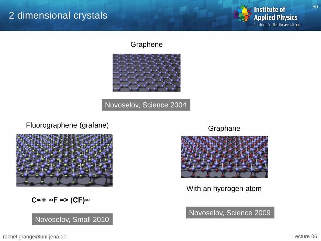
2 dimensional crystals 50
Graphene
Fluorographene (grafane)
C∞+ ∞F => (CF)∞
Graphane
With an hydrogen atom
Novoselov, Small 2010 Novoselov, Science 2009
Novoselov, Science 2004

[email protected] Lecture 06
New class of crystalline materials : 51
2 dimensional atomic crystals
Graphene
Fluorographene (grafane)
Graphane
Boron nitride

[email protected] Lecture 06
Graphene Photonics & Optoelectronics 53
The most transparent conductor
Graphene films were prepared by mechanical exfoliation (repeated peeling) of small mesas of highly oriented pyrolytic graphite
F. Bonaccorso, Z. Sun, T. Hasan, and a C. Ferrari, “Graphene photonics and optoelectronics,” Nature Photonics, vol. 4, no. 9, pp. 611-622, Aug. 2010.

[email protected] Lecture 06
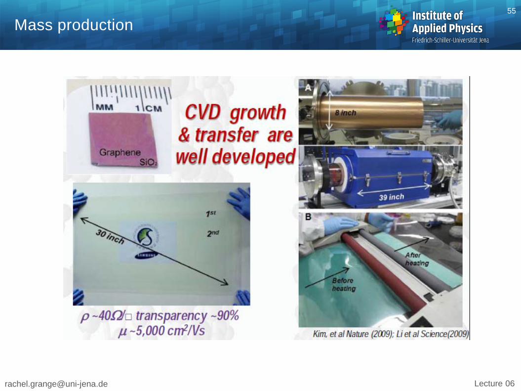
Graphene production 54
Micromechanical cleavage Peeling off a piece of graphite by means of adhesive tape
Liquid-phase exfoliation Ultrasonication in wet environment
Chemical vapor deposition But multilayer

[email protected] Lecture 06
Graphene Photonics & Optoelectronics 57
Photovoltaic devices A photovoltaic cell converts light to electricity
energy conversion efficiency is η = Pmax/Pinc Silicon cell : 25%
Organic & inorganic solar cells
• Transparent conductor window • Photoactive material • Channel for charge transport • Catalyst
η = 0.3 to 1.4% demonstrated

[email protected] Lecture 06
Graphene Photonics & Optoelectronics 58
Touch screen Resistive: transparent conductor needed Capacitive: use the human finger as a conductor
Flexible smart window
[email protected] Lecture 06
Graphene Photonics & Optoelectronics 59
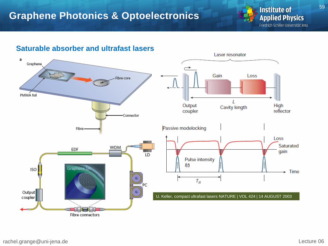
Saturable absorber and ultrafast lasers
U. Keller, compact ultrafast lasers NATURE | VOL 424 | 14 AUGUST 2003

[email protected] Lecture 06
Graphene Photonics & Optoelectronics 60
Optical Limiters high transmittance for low incident light intensity, and low transmittance for high intensity
Optical frequency converter One order larger Chi3 nonlinearity than carbon nanotubes
Terahertz devices Radiation in the 0.3–10 THz range (30 μm to 1 mm) is attractive for biomedical imaging, security, remote sensing and spectroscopy

[email protected] Lecture 06
Graphene Plasmonics 64
Graphene has been recently proposed for plasmon waveguiding at infrared and can be considered as terahertz metamaterials. Photons in the infrared or terahertz domain can be readily coupled to surface plasmons in graphene and form a surface plasmon polariton (SPP) surface wave with many appealing properties:
• such as extreme confinement • tunability via electrical gating or chemical doping • low losses resulting from long lifetime with hundreds of optical cycles.
Intrinsic graphene plasmons

[email protected] Lecture 06
Graphene Plasmonics 65
Intrinsic graphene plasmons millimeter wave band 1 mm to 0.1 mm 300 gigahertz (3×10¹¹ Hz)
Terahertz radiation is strongly absorbed by the atmosphere, limiting communication distance.
Sources: • Quantum cascade lasers • Synchrotron • Free electron laser
What is Terahertz ?

[email protected] Lecture 06
Graphene Plasmonics 66
Graphene-based plasmonics
1. Raman scattering in graphene 2. Plasmonic enhancement of
photovoltage in graphene 3. For modulators and sensors

[email protected] Lecture 06
Outlook 67
Sumio Lijima, Helical microtubules of graphitic carbon, Nature, 354,56,1991 F. Bonaccorso, Z. Sun, T. Hasan, and a C. Ferrari, “Graphene photonics and optoelectronics,” Nature Photonics, vol. 4, no. 9, pp. 611-622, Aug. 2010.
Grigorenko, A. N.; Polini, M.; Novoselov, K. S. Graphene Plasmonics. Nature Photonics 2012, 6, 749–758.
Qiaoliang Bao and Kian Ping Loh, Graphene Photonics, Plasmonics, and Broadband Optoelectronic Devices ACS Nano, 2012, 6 (5), pp 3677–3694
J. W. G. Wildoer, L. C. Venema, A. G. Rinzler, R. E. Smalley, and C. Dekker, “Electronic structure of atomically resolved carbon nanotubes,” Nature, vol. 391, no. 6662, pp. 59–62, 1998.
Andreas Pospischil et al., CMOS-compatible graphene photodetector covering all optical communication bands, Nature Photonics, 7, 892–896, (2013)