Nanolithography Techniques MSE 505 / MSNT...
56
Nanolithography Techniques MSE 505 / MSNT 505 P. Coane
Transcript of Nanolithography Techniques MSE 505 / MSNT...

Nan
olit
ho
gra
ph
y T
ech
niq
ues
MS
E 5
05 /
MS
NT
505
P. C
oan
e

Ou
tlin
e
•W
hat
Is N
ano
tech
no
log
y?
•T
he
Mo
tiva
tio
n F
or
Go
ing
Sm
all
•N
ano
fab
rica
tio
n T
ech
no
log
ies
�B
asic
Tec
hn
iqu
es
�N
ano
Lit
ho
gra
ph
y
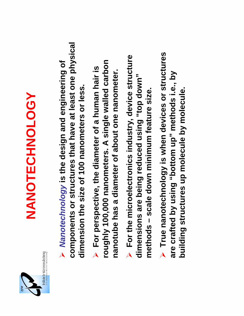
NA
NO
TE
CH
NO
LO
GY
�N
ano
tech
no
log
yis
th
e d
esig
n a
nd
en
gin
eeri
ng
of
com
po
nen
ts o
r st
ruct
ure
s th
at h
ave
at le
ast
on
e p
hys
ical
d
imen
sio
n t
he
size
of
100
nan
om
eter
s o
r le
ss.
�F
or
per
spec
tive
, th
e d
iam
eter
of
a h
um
an h
air
is
rou
gh
ly 1
00,0
00 n
ano
met
ers.
A s
ing
le w
alle
d c
arb
on
n
ano
tub
eh
as a
dia
met
er o
f ab
ou
t o
ne
nan
om
eter
.
�F
or
the
mic
roel
ectr
on
ics
ind
ust
ry, d
evic
e st
ruct
ure
d
imen
sio
ns
are
bei
ng
red
uce
d u
sin
g “
top
do
wn
” m
eth
od
s –
scal
e d
ow
n m
inim
um
fea
ture
siz
e.
�T
rue
nan
ote
chn
olo
gy
is w
hen
dev
ices
or
stru
ctu
res
are
craf
ted
by
usi
ng
“b
ott
om
up
” m
eth
od
s i.e
., b
y b
uild
ing
str
uct
ure
s u
p m
ole
cule
by
mo
lecu
le.

Ch
arac
teri
stic
fea
ture
siz
es t
hat
lie
in t
he
inte
rmed
iate
ran
ge
bet
wee
n
iso
late
d a
tom
s an
d b
ulk
mat
eria
ls (
on
e to
100
nan
om
eter
s) o
ften
dis
pla
y p
hys
ical
att
rib
ute
s su
bst
anti
ally
dif
fere
nt
fro
m t
ho
se d
isp
laye
db
y ei
ther
at
om
s o
r b
ulk
mat
eria
ls.
Dev
elo
pm
ent
Tim
e
Device Size (nm)

NA
NO
TE
CH
NO
LO
GY
Mo
tiva
tio
n T
o G
o S
mal
l
�T
o m
ake
no
vel d
evic
es t
hat
leve
rag
e th
e sp
ecia
l pro
per
ties
of
nan
osc
ale
bu
ildin
g b
lock
s co
nsi
stin
g o
f a
smal
l co
llect
ion
of
ato
ms.
�In
co
ntr
ast
to b
ulk
mat
eria
ls, h
avin
g p
rop
erti
es t
hat
are
d
om
inat
ed b
y n
ove
l qu
antu
m p
hen
om
ena
and
/or
the
effe
cts
of
surf
ace
ener
gy.
�W
hat
has
bee
n g
ain
ed in
th
e la
st 5
0 ye
ars
wit
h d
evic
e sh
rin
kag
e w
ill b
e su
rpas
sed
by
the
ben
efit
s o
f n
ano
mat
eria
lsan
d t
hei
r ar
ran
gem
ent
into
dev
ices
.
�S
up
erio
r se
lect
ivit
y fo
r in
tera
ctio
n, e
nh
ance
d s
ensi
tivi
ty t
o
det
ecti
on
, an
d n
ove
l pro
gra
mm
abili
ty f
or
add
ed s
tru
ctu
ral a
nd
fu
nct
ion
al c
on
tro
l (i.e
. bio
sen
sors
).
�R
evo
luti
on
ary
new
pro
du
cts
usi
ng
new
mat
eria
ls a
nd
su
bst
ance
s n
ot
acce
ssib
le w
ith
oth
er t
ech
no
log
ies

Nan
ote
chn
olo
gy
(Dip
Pen
Nan
olit
ho
gra
ph
y)
(Nan
o-i
mp
rin
t lit
ho
gra
ph
y)
(E-b
eam
an
d X
-ray
N
ano
lith
og
rap
hy)

Nan
oas
sem
bly
Tec
hn
iqu
esL
ayer
-by-
Lay
er A
ssem
bly
Mo
lecu
lar
Rec
og
nit
ion
-Bas
ed S
elf-
Ass
emb
lyS
elf-
Ass
emb
led
Mo
no
laye
rs(S
AM
)N
ano
asse
mb
lyb
y S
tep
-Wis
e P
oly
mer
izat
ion
Nan
op
atte
rnin
gT
ech
niq
ues
X-r
ay L
ith
og
rap
hy
E-b
eam
Lit
ho
gra
ph
yN
ano
imp
rin
tL
ith
og
rap
hy
Mo
lecu
lar
Imp
rin
tin
g
Ele
ctro
less
Dep
osi
tio
n T
ech
niq
ues
Wit
h C
har
ged
Nan
op
arti
cles
Pro
tein
Nan
oen
gin
eeri
ng
Tec
hn
iqu
esC
om
pu
ter-
Aid
ed P
epti
de
Des
ign
Au
tom
ated
Ab
ioti
cP
epti
de
Syn
thes
isB
ioti
c P
epti
de
Syn
thes
is in
Ho
st O
rgan
ism
Nan
om
anu
fact
uri
ng

•N
ot
Just
an
En
gin
eeri
ng
Pro
cess
–F
or
Ato
mic
Sca
le p
reci
sio
n a
nd
co
ntr
ol,
fun
dam
enta
l pri
nci
ple
s o
f p
hys
ics
and
ch
emis
try
mu
st b
e ap
plie
d.
•N
ano
scal
eM
anu
fact
uri
ng
is
Mu
ltid
isci
plin
ary
–In
volv
ing
bu
t n
ot
limit
ed t
o m
ech
anic
s, e
lect
rica
l en
gin
eeri
ng
, ph
ysic
s, c
hem
istr
y, b
iolo
gy,
an
d
bio
med
ical
en
gin
eeri
ng
.
•N
ano
man
ufa
ctu
rin
gis
th
e In
teg
rati
on
o
f E
ng
inee
rin
g, S
cien
ce a
nd
Bio
log
y
Nan
om
anu
fact
uri
ng

Nan
ofa
bri
cati
on
* L
ith
og
rap
hy
InG
ener
al T
erm
slit
ho
gra
ph
y ca
n b
e vi
ewed
as
a p
hys
ical
p
roce
ss in
volv
ing
imag
e tr
ansf
er o
r p
atte
rnin
g in
to v
ario
us
typ
es o
f m
edia
usi
ng
……
……
…
•V
isib
le a
nd
UV
Lig
ht
•E
lect
ron
Bea
m
•Io
n B
eam
•L
aser
•X
-ray
s
•P
reci
sio
n M
ach
inin
g
•P
rin
tin
g
* F
or
Nan
oF
abri
cati
on
A k
ey c
on
sid
erat
ion
is R
eso
luti
on
Pro
cess
Bia
s
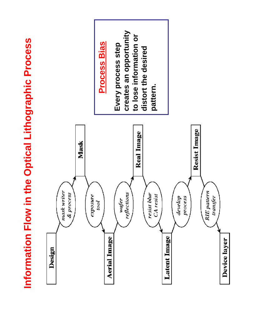
Eve
ry p
roce
ss s
tep
cr
eate
s an
op
po
rtu
nit
y to
lose
info
rmat
ion
or
dis
tort
th
e d
esir
ed
pat
tern
.
Info
rmat
ion
Flo
w in
th
e O
pti
cal L
ith
og
rap
hic
Pro
cess

Op
tica
l Lit
ho
gra
ph
y
Wav
elen
gth
s fo
r o
pti
cal l
ith
og
rap
hy.
Res
olu
tio
n W
min
use
s k 1
= 0.
3 an
d D
OF
use
s k 3
= 1
, ass
um
ing
NA
= 0
.9 f
or
all w
avel
eng
ths
exce
pt
EU
V, w
hic
h a
ssu
med
NA
= 0
.25.
rep
rese
nts
th
e re
lati
ve im
pro
vem
ent
in m
ovi
ng
to
th
e n
ext
gen
erat
ion
wav
e le
ng
th
J. V
ac. S
ci. T
ech
no
l. B
, Vo
l. 21
, No
. 6, N
ov/
Dec
200
3

Op
tica
l Lit
ho
gra
ph
y
Fu
nd
amen
tal L
imit
s to
go
ing
bel
ow
193
nm
•F
or
157
nm
-S
ing
le c
ryst
al c
alci
um
flu
ori
de
len
ses
req
uir
ed
-O
xyg
en a
nd
wat
er v
apo
r ab
sorb
at
this
wav
elen
gth
-C
ost
est
imat
es a
re in
th
e ra
ng
e o
f $2
0 m
illio
n p
er s
can
ner
•F
or
EU
V
-M
ult
i co
ated
ref
lect
ive
mir
rors
req
uir
ed –
up
to
40
laye
rs
-R
efle
ctiv
e m
asks
are
req
uir
ed a
nd
mu
st h
ave
a su
rfac
e
flat
nes
s o
f 5
0 n
m o
r le
ss f
rom
ed
ge
to e
dg
e
-M
ask
surf
aces
can
be
dam
aged
by
oxi
dat
ion
.
-C
ost
est
imat
es a
re f
rom
$40
to
$70
mill
ion
per
sca
nn
er
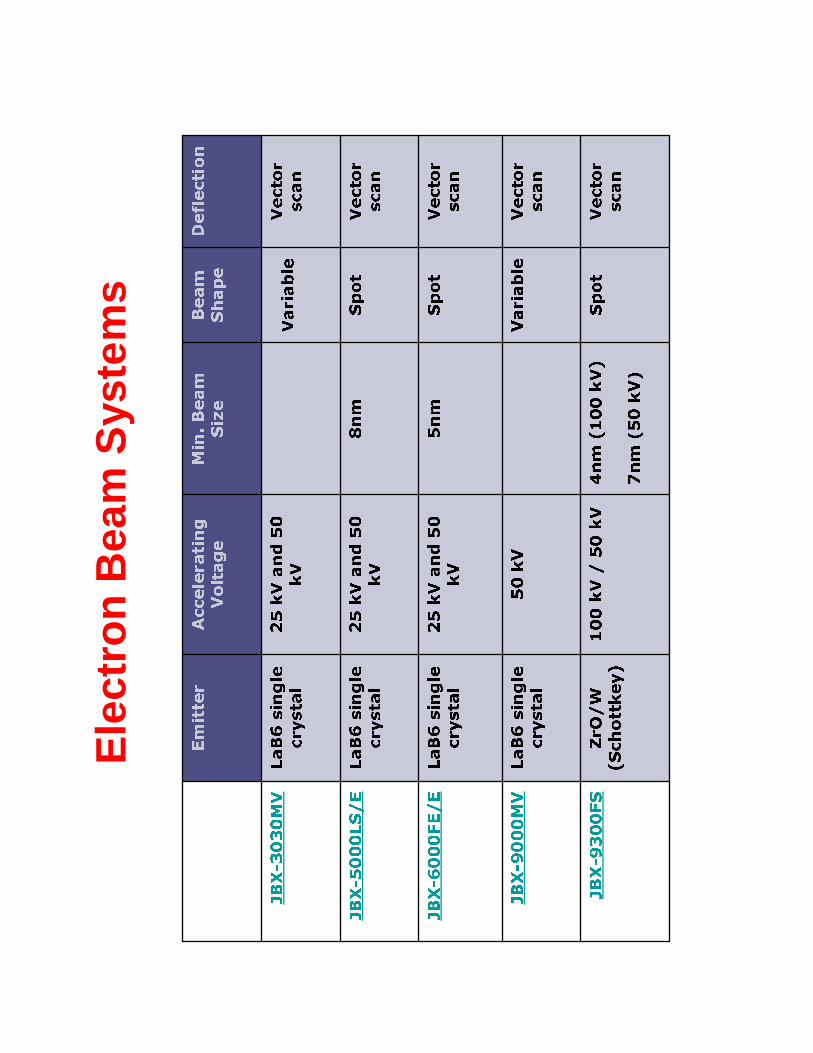
Vecto
r
scan
Sp
ot
4n
m (
10
0 k
V)
7n
m (
50
kV
)
10
0 k
V /
50
kV
ZrO
/W
(S
ch
ott
key)
JB
X-9
30
0FS
Vecto
r
scan
Varia
ble
50
kV
LaB
6 s
ing
le
crysta
lJB
X-9
00
0M
V
Vecto
r
scan
Sp
ot
5n
m2
5 k
V a
nd
50
k
VLaB
6 s
ing
le
crysta
lJB
X-6
00
0FE
/E
Vecto
r
scan
Sp
ot
8n
m2
5 k
V a
nd
50
k
VLaB
6 s
ing
le
crysta
l JB
X-5
00
0LS
/E
Vecto
r
scan
Varia
ble
25
kV
an
d 5
0
kV
LaB
6 s
ing
le
crysta
lJB
X-3
03
0M
V
Defl
ecti
on
Beam
S
hap
eM
in.
Beam
S
ize
Accele
rati
ng
V
olt
ag
eE
mit
ter
Ele
ctro
n B
eam
Sys
tem
s

Ele
ctro
n B
eam
Sys
tem
s

Ele
ctro
n B
eam
Sys
tem
s

Ele
ctro
ns
hav
e a
fin
ite
qu
antu
m m
ech
anic
al w
avel
eng
th:
λ=
1.2
Vb-1
/2
Wh
ich
giv
es a
dif
frac
tio
n li
mit
ed b
eam
siz
e ex
pre
ssed
as:
dd
=0.
6αλ
Ad
d a
ll co
ntr
ibu
tio
ns
to c
alcu
late
th
eore
tica
l min
imu
m b
eam
siz
e:
dd
= (
dg
2+
ds2
+ d
c2+
dd
2 ) 1/
2
Ele
ctro
n B
eam
Siz
e L
imit
s

15 n
m w
ide
go
ld p
alla
diu
m li
nes
, 50
nm
per
iod
icit
y,
PM
MA
res
ist,
fab
rica
ted
by
lift-
off
on
a t
hin
sili
con
n
itri
de
mem
bra
ne
IBM
1. R
ES
. DE
VE
LOP
. V
OL.
32
NO
. 4 J
UL
Y 1
988
Ele
ctro
n B
eam
Nan
olit
ho
gra
ph
y

Nan
ofa
bri
cati
on
E
lect
ron
Bea
m L
ith
og
rap
hy

27 n
m p
erio
d li
nes
exp
ose
d in
30
nm
HS
Q r
esis
t o
n
Si;
(a)
ove
rall
gra
tin
gs
and
(b
) h
igh
er m
agn
ific
atio
n
view
of
ind
ivid
ual
lin
es in
th
e 27
nm
per
iod
gra
tin
g
exp
ose
d a
t a
do
ub
le-p
ass
line
do
se o
f 16
50 n
C/c
m.
30 n
m p
erio
d g
rati
ng
exp
ose
d in
30-
nm
-th
ick
HS
Q r
esis
t o
n S
i; (
a) o
vera
ll g
rati
ng
s, a
nd
(b
) h
igh
er m
agn
ific
atio
n v
iew
of
~10
nm
lin
es a
t 30
nm
per
iod
exp
ose
d a
t 22
00 n
C/c
m.
E-B
eam
Exp
osu
res
in H
ydro
gen
Sils
esq
uio
xan
eR
esis
t
J. V
ac. S
ci. T
ech
no
l. B
21,
No
6.,
No
v/D
ec 2
003

Nan
om
eter
Gra
tin
gs
by
E-b
eam
lith
og
rap
hy
J. V
ac. S
ci. T
ech
no
l. B
, Vo
l. 21
, No
. 6, N
ov/
Dec
200
3
Wid
th o
f in
div
idu
al li
nes
vs
do
se f
or
30, 4
0, a
nd
50
nm
per
iod
icit
y g
rati
ng
s ex
po
sed
in 3
0 n
m o
f H
ydro
gen
Sils
esq
uio
xan
ere
sist
.

Plo
t o
f lin
ewid
thva
riat
ion
fr
om
no
min
al (
i.e.
dev
elo
ped
fo
r th
e ti
me
req
uir
ed t
o c
lear
fea
ture
s)
for
up
to
50%
o
verd
evel
op
men
t. Is
ola
ted
fe
atu
res
stay
wit
hin
a +
/-10
% p
roce
ss w
ind
ow
fo
r fe
atu
res
as s
mal
l as
30 n
m.
Den
se (
line:
spac
era
tio
of
1:3
or
gre
ater
) fe
atu
res
rem
ain
in t
he
pro
cess
w
ind
ow
fo
r fe
atu
res
as
smal
l as
45 n
m.
Nan
olit
ho
gra
ph
yP
roce
ss W
ind
ow C
on
stra
ints

Nan
ofa
bri
cati
on
Ele
ctro
chem
ical
ly G
row
n W
ires
fo
r S
enso
r A
rray
Ap
plic
atio
ns
Nan
oL
ett.
, Vo
l. 4,
No
. 3, 2
004
Sch
emat
ic d
iag
ram
of
a st
ruct
ure
use
d f
or
the
elec
tro
chem
ical
wir
e g
row
th.
(a)
Ele
ctro
dep
osi
ted
wir
e co
nn
ecte
d b
etw
een
ele
ctro
des
. (b
) C
ross
-sec
tio
nal
vi
ew o
f th
e S
isu
bst
rate
, sili
con
nit
rid
e (1
um
), A
u c
on
tact
s, a
nd
th
erm
ally
ev
apo
rate
d S
iO. C
han
nel
s fo
r th
e el
ectr
oly
te s
olu
tio
n a
re f
orm
ed b
etw
een
el
ectr
od
es b
y e-
bea
m p
atte
rnin
go
f th
e S
iO.

Sca
nn
ing
ele
ctro
n m
icro
gra
ph
s o
f d
evic
e p
atte
rns
wit
h f
eatu
re
size
s le
ss t
han
40
nm
ach
ieve
d
by
x-ra
y n
ano
lith
og
rap
hy
follo
wed
by
lifto
ff. T
he
x-ra
y m
ask
is s
ho
wn
on
to
p a
nd
th
e lif
ted
-off
pat
tern
is o
n t
he
bo
tto
m.
Nan
o-p
atte
rnin
g b
y X
-ray
Lit
ho
gra
ph
y

X-r
ay N
ano
lith
og
rap
hy

Nan
o-m
ach
inin
g
By
usi
ng
su
b-n
ano
met
er c
on
tro
l aff
ord
ed b
y A
FM
tec
hn
olo
gy
the
nm
1300
em
plo
ys a
su
btr
acti
ve
ph
oto
mas
kre
pai
r te
chn
iqu
e. T
he
curr
ent
syst
em is
fo
cuse
d o
n m
eeti
ng
req
uir
emen
ts f
or
the
130-
nan
om
eter
des
ign
ru
le n
od
e, b
ut
the
tech
niq
ue
is e
xten
dab
le t
o t
he
100
nm
no
de
and
bey
on
d.
RA
VE
LL
C

Nan
o-m
ach
inin
g o
f M
oS
ion
Qu
artz
Ph
ase
Sh
ifti
ng
Ph
oto
Mas
k

Pro
cess
seq
uen
ce o
f m
ech
anic
al A
FM
lith
og
rap
hy,
lift
-off
an
d p
atte
rn t
ran
sfer
Mec
han
ical
Lit
ho
gra
ph
y b
y A
FM
J. V
ac. S
ci. T
ech
no
l. B
, Vo
l. 16
, No
. 5, S
ep/O
ct 1
998

Th
e s
am
ple
is t
he s
urfa
ce o
f a g
old
crysta
l (A
u(1
11
)) c
overed
wit
h a
self
assem
ble
d
mo
nola
yer (
SA
M) o
f d
ecan
eth
iol
(C
H3
(C
H2
)9
SH
).
Im
ag
ing
was d
on
e u
nd
er
liq
uid
in
a s
olu
tion
con
tain
ing
octa
decan
eth
iol(C
H3
(C
H2
)1
7S
H).
Th
e
lith
og
rap
hy w
as d
on
e b
y a
pp
lyin
g a
n
ap
proxim
ate
ly 1
0X
hig
her f
orce d
urin
g
writ
ing
. Th
is d
isp
laced
th
e d
ecan
eth
iol
mole
cu
les,
wh
ich
were t
hen
rep
laced
in
th
e S
AM
by t
he lon
ger o
cta
decan
eth
iol
mole
cu
les.
Th
e s
urfa
ce is h
igh
er w
here
writ
ten
becau
se t
he t
ails o
f th
e
octa
decan
eth
iol
mole
cu
les s
tick u
p a
bove
the a
verag
e h
eig
ht
of
the S
AM
. Tota
l siz
e
of
the s
pir
als
is 6
20
nm
. A
verag
e lin
e
sp
acin
g is 4
0n
m a
nd
averag
e lin
e-w
idth
s
(FW
HM
) a
re 1
5 t
o 2
0n
m.
Nan
olit
ho
gra
ph
yA
FM
Nan
og
raft
ing
of
Th
iols
on
a A
u(1
11)
Su
rfac
e
M. L
iu a
nd
G. L
iu, U
C D
avis

Nan
olit
ho
gra
ph
y u
sin
g A
no
dic
Oxi
dat
ion
Wh
en t
he
AF
M t
ip is
bro
ug
ht
clo
se t
o t
he
surf
ace,
wat
er f
rom
th
eam
bie
nt
hu
mid
ity
form
s a
dro
ple
t b
etw
een
th
e ti
p a
nd
th
e su
bst
rate
. To
dri
ve t
he
ano
dic
oxi
dat
ion
pro
cess
, a v
olt
age
(5 t
o 1
5 vo
lts)
is a
pp
lied
bet
wee
n t
he
tip
an
d t
he
sub
stra
te. T
he
hig
h e
lect
ric
fiel
d io
niz
es t
he
wat
er d
rop
let
and
th
e O
H-
ion
s p
rod
uce
d p
rovi
de
the
oxi
dan
t fo
r th
e ch
emic
al r
eact
ion
.

Th
e N
otr
e D
ame
log
o s
ho
ws
2nm
th
ick
oxi
de
gro
wn
on
a T
i film
. O
xid
atio
n is
per
form
ed b
y ap
ply
ing
a p
ote
nti
al t
o a
co
nd
uct
ing
AF
M t
ip
and
usi
ng
th
e co
nd
ense
d w
ater
dro
ple
t at
th
e ti
p a
s an
ele
ctro
chem
ical
ce
ll. T
he
oxi
diz
ed r
egio
n g
row
s, r
esu
ltin
g in
rai
sed
su
rfac
e fe
atu
res.
Nan
olit
ho
gra
py
–A
no
dic
Oxi
dat
ion
EE
Dep
artm
ent
Un
iv. o
f N
otr
e D
ame
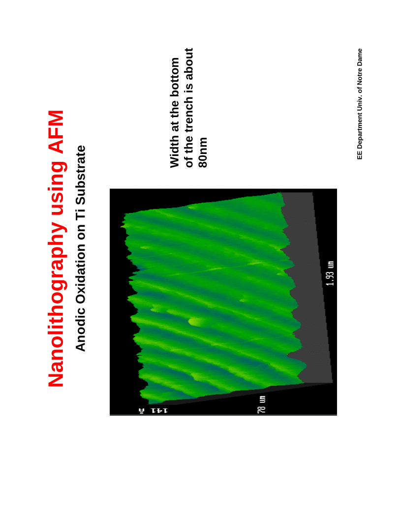
Nan
olit
ho
gra
ph
y u
sin
g A
FM
An
od
ic O
xid
atio
n o
n T
i Su
bst
rate
Wid
th a
t th
e b
ott
om
o
f th
e tr
ench
is a
bo
ut
80n
m
EE
Dep
artm
ent
Un
iv. o
f N
otr
e D
ame

Th
e w
idth
at
the
top
of
the
lines
is
abo
ut
70n
m
EE
Dep
artm
ent
Un
iv. o
f N
otr
e D
ame
Nan
olit
ho
gra
ph
y u
sin
g A
FM
An
od
ic O
xid
atio
n -
Ti S
ub
stra
te

Nan
olit
ho
gra
ph
y u
sin
g a
n S
TM
Sch
emat
ic d
iag
ram
of
the
exp
erim
enta
l set
-up
fo
r si
lico
n o
xid
e re
mo
val b
y fi
eld
em
itte
d e
lect
ron
bea
m ir
rad
iati
on
at
an e
leva
ted
te
mp
erat
ure
usi
ng
a S
can
nin
g T
un
nel
ing
Mic
rosc
op
e (S
TM
).
(1)
Th
e o
xid
e la
yer
wit
hin
th
e e-
bea
m-e
xpo
sed
ar
ea is
dec
om
po
sed
an
d r
edu
ced
(2)
Th
e re
du
ced
SiO
is
chan
ged
to
vo
lati
le S
iOan
d e
vap
ora
ted
fro
m
the
surf
ace
at e
leva
ted
te
mp
erat
ure
s.
Nan
ote
chn
olo
gy
14 (
2003
) R
55–R
62

Th
e q
uan
tum
yie
ld f
or
imp
act-
ind
uce
d S
iO2
dec
om
po
siti
on
as
a fu
nct
ion
of
the
e-b
eam
ki
net
ic e
ner
gy
wit
h b
eam
cu
rren
ts o
f 10
nA
(◦),
20
nA
(♦),
30
nA
(), 4
0 n
A()
an
d 5
0 n
A(×
). T
he
solid
cu
rve
rep
rese
nts
th
e su
bst
anti
al y
ield
.
Nan
olit
ho
gra
ph
y o
n S
iO2
usi
ng
an
ST
M
Nan
o-f
abri
cati
on
of
pat
tern
s b
y P
C
con
tro
l of
the
ST
M t
ip p
osi
tio
n.
Sm
alle
st li
new
idth
= 25
nm
Nan
ote
chn
olo
gy
14 (
2003
) R
55–R
62

ST
Mim
age
of
a p
oly
pro
pyl
ene
mo
lecu
le o
n g
rap
hit
e.
Nan
ofa
bri
cati
on
on
th
e M
ole
cula
r S
cale

Nan
ofa
bri
cati
on
on
th
e M
ole
cula
r S
cale

(a)
Sch
emat
ic d
iag
ram
of
the
dev
ice.
Th
e su
spen
ded
bri
dg
e co
nsi
sts
of
har
d b
aked
ph
oto
resi
sto
r S
iO2,
an
d e
vap
ora
ted
Si(
or
SiN
). (
b)
Sca
nn
ing
-ele
ctro
n-
mic
rosc
op
e (S
EM
) im
age
of
the
dev
ice
that
h
as a
co
nta
ct a
rea
of
400
nm
2. F
or
clar
ity
in S
EM
imag
ing
, sam
ple
s w
ere
tilt
ed 4
5°. (
c) S
EM
imag
e th
at s
ho
ws
that
th
e to
p s
urf
ace
is f
ar a
way
fro
m t
he
sub
stra
te (
> 50
0 n
m)
and
th
at t
he
sup
po
rtin
g
mid
dle
laye
r fe
atu
res
a la
rge
un
der
cut.
Th
us,
we
can
mea
sure
th
etr
ansp
ort
pro
per
ties
of
the
dev
ices
wit
ho
ut
a lif
toff
ste
p in
th
e fa
bri
cati
on
.N
ano
Let
t., V
ol.
3, N
o. 2
,200
3
Th
e el
ectr
on
ic t
ran
spo
rt
char
acte
rist
ics
of
self
-ass
emb
led
m
on
ola
yers
of
ph
enyl
ene-
bas
ed ð
-co
nju
gat
ed m
ole
cule
s w
ere
mea
sure
d in
a t
hre
e t
erm
inal
dev
ice
geo
met
ry. T
he
sho
rt (
1 n
m)
mo
lecu
les
wer
e co
nn
ecte
d b
etw
een
tw
o g
old
ele
ctro
des
wit
h a
nea
rby
Al 2
O3/
Al g
ate
elec
tro
de.
It w
as
po
ssib
le t
o f
abri
cate
wo
rkin
g
dev
ices
usi
ng
th
ree
of
the
five
m
ole
cule
s in
vest
igat
ed. T
he
oth
er
two
typ
es o
f m
ole
cule
s le
d t
o
dev
ices
wh
ere
the
Au
ele
ctro
des
w
ere
sho
rted
to
get
her
. Fo
r d
evic
es
wit
h 1
,3-b
enze
ned
ith
iol,
a w
eak
gat
e ef
fect
was
ob
serv
ed.
Nan
ofa
bri
cati
on
SA
M o
f P
hen
ylen
e-B
ased
Co
nju
gat
ed M
ole
cule
s in
an
FE
T g
eom
etry

Nan
ofa
bri
cati
on
on
th
e A
tom
ic S
cale

In t
he
con
stan
t tu
nn
elin
g c
urr
ent
mo
de
of
op
erat
ion
, a v
olt
age
Vz
is
app
lied
to
th
e Z
pie
zoel
ectr
ic e
lem
ent
by
mea
ns
of
the
con
tro
l un
it C
U t
o
keep
th
e tu
nn
elin
g c
urr
ent
con
stan
t w
hile
th
e ti
p is
sca
nn
ed a
cro
ss t
he
surf
ace
by
alte
rin
g V
xan
d V
y. T
he
trac
e o
f th
e ti
p, a
y-s
can
, gen
eral
ly
rese
mb
les
the
surf
ace
top
og
rap
hy.
Ele
ctro
nic
inh
om
og
enei
ties
als
o
pro
du
ce s
tru
ctu
re in
th
e ti
p t
race
, as
illu
stra
ted
on
th
e ri
gh
tab
ove
wit
h
two
su
rfac
e at
om
s h
avin
g e
xces
sive
neg
ativ
e ch
arg
e.
Sca
nn
ing
Tu
nn
elin
g M
icro
sco
pe

Nan
op
atte
rnin
go
n t
he
Ato
mic
Sca
le
Usi
ng
a S
can
nin
g T
un
nel
ing
Mic
rosc
op
e (S
TM
)
IBM
199
0X
eno
n A
tom
s
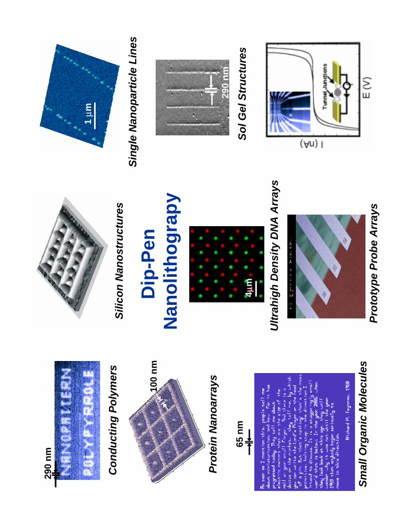
Ult
rah
igh
Den
sity
DN
A A
rray
s
So
l Gel
Str
uct
ure
s
Pro
tein
Nan
oar
rays
Sm
all O
rgan
ic M
ole
cule
s
100
nm
4µm
Co
nd
uct
ing
Po
lym
ers
290
nm
Dip
-Pen
N
ano
lith
og
rap
y
Pro
toty
pe
Pro
be
Arr
ays
1 µm
65 n
m
Sin
gle
Nan
op
arti
cle
Lin
es
290
nm
Sili
con
Nan
ost
ruct
ure
s

Bo
tto
m-U
p N
ano
fab
rica
tio
n v
ia
Dip
-Pen
Nan
olit
ho
gra
py
Bu
ildin
g B
lock
s
DP
N-G
ener
ated
Su
rfac
e T
emp
late
sA
dd
ress
able
Mat
eria
ls w
ith
Wel
l-D
efin
edS
up
erst
ruct
ure
s an
d O
rien
tati
on
s

Lif
e S
cien
ces
Mic
roel
ectr
on
ics
(Bio
)sen
sor
Dev
ices
•si
ng
le m
ole
cule
stu
die
s•
stru
ctu
re/f
un
ctio
n•
dru
g d
isco
very
•u
ltra
-hig
h d
ensi
ty g
ene
chip
s•
pro
teo
mic
s/p
epti
de
arra
ys•
cell
pro
cess
es (
adh
esio
n)
•vi
rus/
pro
tein
cry
stal
lizat
ion
scie
nce
& t
ech
no
log
ysc
ien
ce &
tec
hn
olo
gy
•m
ole
cula
r el
ectr
on
ics
•n
ano
scal
esu
rfac
e p
hen
om
ena
•o
rgan
ic e
tch
res
ists
•p
rin
ted
nan
oca
taly
sts
•co
mb
inat
ori
al m
ater
ials
dis
cove
ry•
CN
T, n
ano
wir
ed
evic
es•
add
itiv
e p
ho
tom
ask
rep
air
•ci
rcu
it e
dit
•sp
intr
on
icd
evic
es•
gas
/ch
emo
sen
sors
DP
N:
A V
ersa
tile
To
ol F
or
Nan
ofa
bri
cati
on
CO
NV
ER
GE
NC
E o
f fi
eld
s fr
om
th
e “
BO
TT
OM
UP
”

Tw
o F
un
dam
enta
l Typ
es o
f D
ip-P
en
Nan
olit
ho
gra
ph
y M
eth
od
s
•D
irec
t W
rite
–w
rite
th
e m
ole
cule
of
inte
rest
dir
ectl
y o
nto
th
e su
rfac
e as
th
e in
k•
Tem
pla
tin
g–
wri
te o
ut
an in
k p
atte
rn in
ord
er t
o
fab
rica
te o
r at
tach
so
met
hin
g e
lse

Dip
-Pen
Nan
olit
ho
gra
ph
y
Flo
rid
a S
tate
Un
iver
sity
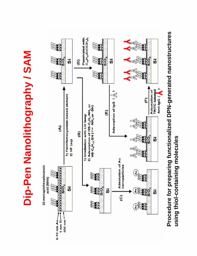
Dip
-Pen
Nan
olit
ho
gra
ph
y / S
AM
16-m
erca
pto
hex
adec
ano
ic
acid
(M
HA
)
Pro
ced
ure
fo
r p
rep
arin
g f
un
ctio
nal
ized
DP
N-g
ener
ated
nan
ost
ruct
ure
s u
sin
g t
hio
l-co
nta
inin
g m
ole
cule
s

Dip
-Pen
Nan
olit
ho
gra
ph
y / S
AM
AF
M t
op
og
rap
hic
imag
es o
f th
e et
ched
MH
A/A
u/T
i/SiO
x/S
in
ano
stru
ctu
res,
lin
es (
A)
and
do
ts (
B),
bas
ed o
n t
he
DP
N o
f M
HA
o
n a
go
ld s
urf
ace

AF
M t
op
og
rap
hic
imag
es o
f in
div
idu
al A
u n
ano
par
ticl
esad
sorb
ed o
n H
S-S
AM
-mo
dif
ied
nan
op
atte
rns
of
lines
(A
, wit
h h
igh
-res
olu
tio
n im
age
inse
rted
) an
d d
ots
(B).
Dip
-Pen
Nan
olit
ho
gra
ph
y / S
AM

ME
GA
ped
e™
~1.3
Mill
ion
DP
N P
en A
rray
(co
urt
esy
of
Nan
oIn
k, In
c.)

ME
GA
ped
e-
DP
NS
tam
per
™
Flu
ore
scen
t ar
rays
dep
osi
ted
by
a M
EG
Ap
ede
DP
NS
tam
per
ME
GA
ped
ep
rob
e ar
ray

Nan
ofa
bri
cati
on
Usi
ng
Sel
f A
ssem
bly
Th
e su
bst
rate
is f
un
ctio
nal
ized
w
ith
org
anic
mo
lecu
les
to
pro
du
ce p
ola
r an
d n
on
-po
lar
reg
ion
s. C
arb
on
nan
otu
bes
in
solu
tio
n a
re a
ttra
cted
to
th
e p
ola
r re
gio
ns
and
sel
ecti
vely
se
lf a
ssem
ble
on
th
e su
bst
rate
fo
llow
ing
th
e lit
ho
gra
ph
ical
ly
def
ined
pat
tern
s.
Mas
s p
rod
uct
ion
of
carb
on
n
ano
tub
eb
ased
cir
cuit
st
ruct
ure
s is
po
ssib
le
Su
rfac
e F
un
ctio
nal
izat
ion
SW
CN
T S
elf
Ass
emb
ly
Po
lar
Mo
lecu
lar
Pat
tern
sN
on
-Po
lar
Reg
ion
SW
CN
T S
usp
ensi
on
Su
bst
rate

Fab
rica
tio
n s
equ
ence
fo
r th
ree
dif
fere
nt
vari
etie
s o
f im
pri
nt
lith
og
rap
hy.
Imp
rin
t L
ith
og
rap
hy

Nan
ofa
bri
cati
on
Usi
ng
Ste
p-a
nd
Fla
sh
Imp
rin
t L
ith
og
rap
hy
1.U
sin
g a
pre
cise
pie
zo-d
rive
n d
isp
ense
h
ead
, a s
ilico
n-r
ich
, lo
w-v
isco
sity
, p
ho
tocu
rab
le, m
on
om
er s
olu
tio
n is
d
isp
ense
d o
nto
th
e su
bst
rate
in t
he
reg
ion
wh
ere
the
pat
tern
is t
o b
e p
rin
ted
.
2.T
he
tem
pla
te is
th
en p
ress
ed in
to c
on
tact
w
ith
th
e w
afer
usi
ng
ver
y lo
w p
ress
ure
s (<
1psi
) to
sp
read
th
e liq
uid
acr
oss
th
e fi
eld
an
d f
ill t
he
tem
pla
te's
rel
ief.
3.U
V li
gh
t is
irra
dia
ted
th
rou
gh
th
e b
ack
of
the
tem
pla
te, c
uri
ng
th
e m
on
om
er.
4.T
he
tem
pla
te, p
re-c
oat
ed w
ith
a
flu
oro
carb
on
rel
ease
ag
ent,
is r
emo
ved
, le
avin
g t
he
cure
d, p
atte
rned
res
ist
laye
r b
ehin
d.
5.F
inal
ly, a
bre
akth
rou
gh
etc
h p
assi
ng
th
rou
gh
th
e re
sid
ual
etc
h b
arri
er a
nd
a
tran
sfer
laye
r (a
ny
org
anic
sp
in-c
oat
ed
resi
n s
uch
as
an a
nti
refl
ecti
ve c
oat
ing
, A
RC
) tr
ansf
ers
the
hig
h a
spec
t ra
tio
pat
tern
to
th
e su
bst
rate
.
So
lid S
tate
Tec
hn
olo
gy
Feb
ruar
y 20
04

100,
60,
30,
an
d 2
0 n
m f
eatu
res
def
ined
usi
ng
th
e IT
O-b
ased
pro
cess
.
Tem
pla
te p
atte
rn t
ran
sfer
seq
uen
ce f
or
30 n
m f
eatu
res.
Ste
p a
nd
Fla
sh N
ano
-Im
pri
nt
Lit
ho
gra
ph
y
J. V
ac. S
ci. T
ech
no
l. B
, Vo
l. 21
, No
. 6, N
ov/
Dec
200
3

Pri
nte
d f
eatu
res
in t
he
acry
late
-bas
ed e
tch
bar
rier
. (a)
To
p-d
ow
n S
EM
s.
(b)
Cro
ss-s
ecti
on
al im
ages
of
bo
th s
ing
le t
ier
and
mu
lti-
tier
ed f
eatu
res.
Ste
p a
nd
Fla
sh N
ano
-Im
pri
nt
Lit
ho
gra
ph
y
J. V
ac. S
ci. T
ech
no
l. B
, Vo
l. 21
, No
. 6, N
ov/
Dec
200
3

Mu
lti-
tier
ed s
tru
ctu
res
form
ed b
y it
erat
ing
th
e fa
bri
cati
on
pro
cess
.
Imp
rin
t L
ith
og
rap
hy
for
Ap
plic
atio
n t
o
Inte
gra
ted
Cir
cuit
Fab
rica
tio
n