NanoLab Talk - Politecnico di Milano · Metallization of stretchable polymers - the new generation...
57
NanoLab Talk Department of Energy, Politecnico di Milano 2018 - 2019
Transcript of NanoLab Talk - Politecnico di Milano · Metallization of stretchable polymers - the new generation...

NanoLab Talk Department of Energy, Politecnico di Milano
2018 - 2019

NanoLab Talks are periodic seminars organized within the activities of the NanoLab group at the
Department of Energy at Politecnico di Milano, Italy. The talks are given by experts from academy, research
centers and private companies on Education, Science and Technology.
The topics spread on different aspects of physics, engineering, materials science, nanotechnology,
chemistry and education to a target audience composed by master thesis students, PhDs, post docs,
technicians and researchers.
NanoLab Talks are given in seminar room at Building 19 (Leonardo campus) of the Department of Energy,
Politecnico di Milano.
This document reports the abstracts of the 18 and 21 talks we had in 2018 and in 2019 in chronological
order.

NanoLab Talk 2018 List of speakers
Speaker Title Affiliation
Tommaso Del Rosso
Laser based Synthesis and Characterization of Nanomaterials
Pontifical Catholic University of Rio de Janeiro
Luca Bettini Cluster-assembled carbon materials (and devices) for sustainable energy applications
Università Statale di Milano
Davide Proserpio Perchè citiamo? L’etica delle citazioni e gli (ipotetici) allotropi del carbonio
Università Statale di Milano
Arianna Formenti Theoretical investigations of laser-driven ion acceleration with nanostructured materials
Politecnico di Milano NanoLab
Alberto Naldoni Photocatalysis in the hot spot: metal-semiconductor hybrids for plasmon-enhanced chemical reactions
Regional Centre of Advanced Technologies and Materials, Czech Rep.
Alessandro Maffini On the growth dynamics of low-density carbon foams in Pulsed Laser Deposition experiments
Politecnico di Milano NanoLab
Gianluigi Botton High-Resolution Electron Microscopy and Spectroscopy: Applications to Energy-related Materials and Devices
McMaster University, Canada
Luca Ravagnan Metallization of stretchable polymers - the new generation of leads for Neuromodulation and Neuromonitoring
WISE srl
Francesco Minuto Porous carbon materials for gas adsorption Politecnico di Torino
Francesca Borghi Solid-like transition of ionic liquids in nanostructured carbon thin films
Università Statale di Milano
H. Nishimura Recent activities on laser-driven neutron sources at ILE, Osaka
Fukui University, Japan
Alessandro Molle Designer artificial 2D materials IMM - CNR
Andrea Pazzaglia Measuring thin films mass thickness through energy dispersive x-ray spectroscopy
Politecnico di Milano NanoLab
Gianlorenzo Bussetti
The solid-liquid interface and nanomicroscopy (solinano) lab: current activities of the new inter-departmental facility
Politecnico di Milano
Dept. of Physics
Matteo Ghidelli Novel thin film metallic glasses with unique mechanical properties
Politecnico di Milano NanoLab
Sergio Tosoni Modelling Oxide Surfaces at the 2D Limit Università di Milano-Bicocca
Rik Tykwinski Cumulenes and polyynes as carbon atomic wires University of Edmonton, Canada
Luca Fedeli Superintense laser interaction with nanostructured targets Politecnico di Milano NanoLab

NanoLab Talk 2019 - List of speakers
Speaker Title Affiliation
Cristian Manzoni Hyperspectral Imaging and Microscopy National Research Council - CNR
Yitzhak Maron Determination of the ion temperature in a high-energy-density plasma using Stark effect
Weizmann Institute of Science, Israel
Claudia Conti Micro Spatially Offset Raman Spectroscopy for the investigation of materials subsurface
National Research Council - CNR
Paolo Piseri Synchrotron-radiation for the investigation of free nanoparticles in a molecular beam
Università Statale di Milano, Dept. of Physics
Christoph Gadermaier
Non-equilibrium Photophysics of Layered Two-dimensional Semiconductors and their Heterostructures
Politecnico di Milano, Dept. of Physics
Andrea Pola Nuclear Measurements Group @ PoliMi: recent developments and open questions
Politecnico di Milano, Dept. of Energy
Andrea Ferrari Light Scattering and Emission from Hetero-structures Univ. of Cambridge, UK
Fabrizio Siviero Recent developments in Non-Evaporable Getter technology and application in vacuum systems from HV to XHV
SAES Getters s.p.a.
Paolo Gondoni Teaching quantum physics in high school: a low-cost experimental approach
IIS Badoni (Lecco)
Mario Caironi Printed Polymer Electronics Italian Institute of Technology-IIT
Alessandro Bailini
Induction Assisted Laser Welding
of High Thickness Steel Blue Think s.p.a.
Jean Marie Nsanzimana
Earth-abundant Metal-metalloid Materials as Efficient Oxygen-Evolving Electrocatalyst
NTU, Singapore
Alessio Lamperti Extended MoS2 monolayer growth using chemical vapor deposition on flat and patterned substrates
National Research Council - CNR
Riccardo Bertacco
Spin-wave nano-optics for analog computing: an emerging technology born in Polifab
Politecnico di Milano Dept. of Physics
Orbelli Biroli Push-pull porphyrins: from NLO properties to photoelectrochemical cell applications
National Research Council - CNR
Andrea Picone Atomic and molecular diffusion on solid surfaces Politecnico di Milano, Dept. of Physics
Federico Picollo Mev-ion-beam Lithography in Diamond for Applications in Bio-sensing
Università di Torino, Dept. of Physics

Guido Fratesi Organic molecules at surfaces: insight from theoretical core-level spectroscopy
Università Statale di Milano, Dept. of Physics
Luca Mascaretti Plasmonic titanium nitride thin films and nanostructures for light-to-heat energy conversion
Regional Centre of Advanced Technologies and Materials, Czech Republic
Piero Mazzolini Growth and Characterization of Epitaxial Ga2O3 Thin Films via Molecular Beam Epitaxy
Paul Drude Institute, Berlin Germany
Francesco Scotognella
Doped semiconductor nanocrystals as plasmonic materials for photonics and hot electron extraction
Politecnico di Milano Dept. of Physics

Monday, January 15th, 2018 – 15.30 Seminar Room
Department of Energy – Cesnef (Building 19) via Ponzio 34/3 Milan Politecnico di Milano
“Laser based Synthesis and Characterization of Nanomaterials”
Prof. Tommaso Del Rosso
NanoLaserLab – Laboratory of Laser based Synthesis and Characterization of Nanomaterials
Department of Physics Pontifical Catholic University of Rio de Janeiro
Abstract: Localized or propagative Surface Plasmon Resonances (SPR) are at today widely investigated and
used for enhanced optical spectroscopy and optical (bio-)sensing. Among different techniques
used for the synthesis of metal nanomaterials, Pulsed Laser Ablation in Liquids (PLAL) appears one
of the most promising in terms of bio-compatibility and versatility, allowing the green synthesis of
a large gamma of metal nanoparticles (NPs) and metal-dielectric nanocomposites (NCs). After a
general introduction on the concepts of SPR resonances and state of art of PLAL, the talk will be
focused on the recent advances on the synthesis and applications of colloidal dispersions of Metal-
Carbynoid NCs by PLAL, followed by a description of the potentialities of SPR spectroscopy in the
all optical characterization of metal nanoparticles.
------------------------------------ For further information [email protected]
NanoLab Talk
Tuesday, February 6th, 2018 – 15.00 Seminar Room
Department of Energy – Cesnef (Building 19) via Ponzio 34/3 Milano Politecnico di Milano - Italy
“Cluster-assembled carbon materials (and devices) for sustainable energy applications”
Luca Bettini
LGM laboratory - CIMaINa
Physics Department, University of Milano Abstract: The fabrication of nanostructured materials by the direct deposition of nanoparticles from the gas-phase enables the nano- and micro-manufacturing of complex systems with functional capabilities. Among different methods the assembling of gas-phase clusters and nanoparticles produced in a Pulsed Microplasma Cluster Source (PMCS) and deposited by Supersonic Cluster Beam Deposition (SCBD) is a versatile approach that allows the growth of nanostructured materials with controlled physico-chemical properties and their integration into microfabricated devices. Here we present the SCBD/PMCS synthesis of cluster-assembled carbon thin films and nanocomposites where the structural properties are determined not only by the characteristics of the clusters produced in the gas-phase but also by their organization upon deposition. As prepared carbon-based materials typically present very low density, high surface roughness and large porosity that are promising for the fabrication of electrochemical devices for sustainable energy technologies, such as electrolyte-gated transistors, supercapacitors and photocatalytic systems.
------------------------------------ For further information [email protected]

NanoLab Talk
Lunedì, 9 Aprile, 2018 – 14.30 Aula Seminari 1° piano
Dipartimento di Energia – Cesnef (Edificio 19) via Ponzio 34/3 Milano Politecnico di Milano
“Perchè citiamo? L'etica delle citazioni e gli (ipotetici) allotropi del carbonio”
Prof. Davide M. Proserpio
Universita' degli Studi di Milano,
Dipartimento di Chimica
Abstract: Fare calcoli di chimica quantistica è oggi una routine, ed è molto più facile che condurre esperimenti. Ergo, centinaia di articoli dedicati a strutture ipotetiche tridimensionali del carbonio elementare (delle quali conosciamo il diamante e la grafite) proliferano nella letteratura scientifica. Questi articoli proclamano enfaticamente i propri meriti, primo fra tutti la “novità”. Eppure metà di quelle strutture, pur belle che siano, sono già state pubblicate, all’insaputa degli autori, non per malizia, ma solo per pigrizia. Come è potuto succedere, quando tutti dispongono di computer sempre più potenti e di strategici, arguti motori di ricerca come Google Scholar, SciFinder, Web of Science, Scopus, che il processo di citazione sia fallito ripetutamente e queste strutture siano state descritte come nuove quando in effetti non lo erano? E’ troppo facile accusare una mancanza di educazione nell’arte della ricerca bibliografica, che nondimeno deve essere insegnata ai tempi di SciFinder così come lo era ai tempi dei Chemical Abstracts accumulati sui nostri scaffali. Pensiamo che entri in gioco un fattore psicologico più complesso, derivante dall’interazione uomo-macchina: vediamo il potere dei computer nei calcoli ma anche nell’organizzare liste e testi. Ci lasciamo cullare dall’efficienza delle macchine e dimentichiamo che se immettiamo spazzatura - la nostra domanda mal formulata – ne esce spazzatura. Per aiutare i ricercatori abbiamo messo a punto uno strumento online, SACADA (sacada.sctms.ru), che raccoglie e confronta le strutture ipotetiche degli allotropi del carbonio. rif: Homo Citans and Carbon Allotropes: For an Ethics of Citation R. Hoffmann, A. A. Kabanov, A. A. Golov, D. M. Proserpio, Angew. Chem. Int. Ed. 2016, 55, 10962-10976. ------------------------------------ Per infomazioni: [email protected]

NanoLab Talk Monday, 23rd April, 2018 – 14.30
Seminar Room 1° floor Department of Energy – Cesnef (Building 19) via Ponzio 34/3 Milan
Politecnico di Milano
“Theoretical investigations of laser-driven ion acceleration with nanostructured materials”
Arianna Formenti
NanoLab – Department of Energy
Politecnico di Milano
Abstract: Laser-plasma ion source have a great potential for a number of foreseen applications (e.g. ion beam analysis and neutron generation) because of their unique properties and the possibility to use compact, table-top laser systems as drivers. Irradiating a solid foil with an ultra-intense (I>1018W/cm2) and ultra-short (~10fs - 1ps) laser pulse it is possible to accelerate ions up to 10MeV/nucleon energies. However, many challenges still need to be faced to make the potential applications a reality. Major improvements in the acceleration process, i.e. increase of ion maximum energy and total charge, can be obtained using advanced targets, without raising laser requirements. In this contribution I present a brief overview of enhanced laser-driven ion acceleration with a special advanced target concept: foam-based multilayer targets. They consist in thin solid foils coated with an ultra-low density (10-20 mg/cm3) nanostructured Carbon layer. In this condition, the foam density matches the critical plasma density for typical Ti:Sapphire laser systems. This leads to an enhanced laser-plasma coupling and, ultimately, to an improved acceleration process. I will shortly discuss this topic in relation to the research activity that I have been conducting during the first half of my PhD program: • Particle-In-Cell simulations designed to investigate the physics of the interaction with target materials with a structure on the sub-micrometer scale; • Simplified analytical models used to determine whether specific non-Maxwellian, relativistic electron populations may influence the acceleration performances; • Multi-stage simulations of laser-plasma interaction and radiation-matter interaction, in cascade, designed to assess the feasibility of secondary neutron generation. ------------------------------------ Per infomazioni: [email protected]

NanoLab Talk
Monday, 14th may, 2018 – 14.30 Seminar Room 1° floor
Department of Energy – Cesnef (Building 19) via Ponzio 34/3 Milan Politecnico di Milano
“Photocatalysis in the hot spot:
metal-semiconductor hybrids for plasmon-enhanced
chemical reactions”
Alberto Naldoni
Regional Centre of Advanced Technologies and Materials, Faculty of Science, Palacky University,
Šlechtitelů 27, 78371 Olomouc, Czech Republic Abstract: The use of plasmonic nanoantennas in solar energy conversion has recently focused on processes that generate hot carriers through the metal-semiconductor interface. In this talk, I will cover several topics in plasmon-enhanced catalysis, from advanced characterization methods to applications. I will start showing how it is possible to detect, with atomistic resolution, the orbitals that are involved in the hot electron transfer at the Au/TiO2 interface and discuss the implications for sustainable catalytic processes. I will also discuss how the interaction between plasmonic and doped TiO2 nanoparticles influences the mechanism of plasmon-enhanced selective oxidations and hydrogen production. In the second part of the talk, I will present our recent results on ultrathin hematite films for water splitting used as dielectric layer in gap plasmon structures. Several designs including metallic and high index nanoresonators will be analyzed and results will be discussed in terms of types of plasmonic resonances, physics of electric field enhancement and hot electron generation. Finally, I will talk about refractory titanium nitride (TiN) as an emerging alternative plasmonic material and its superior performance for solar water splitting.
------------------------------------ For further information: [email protected]
NanoLab Talk
Monday, 21st may, 2018 – 15.00 Seminar Room 1° floor
Department of Energy – Cesnef (Building 19) via Ponzio 34/3 Milan Politecnico di Milano
“On the growth dynamics of low-density carbon
foams in Pulsed Laser Deposition experiments”
Alessandro Maffini
NanoLab – Department of Energy
Politecnico di Milano Abstract: Ultra-low density porous materials (1-20 mg/cm3, also known as “foams”) show unique appealing features, such as a nearly perfect black body behaviour and an extremely high surface-to-volume ratio. Among them, carbon (C) foams have attracted great interest in cutting-edge research topics such as the generation of hadron beams via laser-plasma acceleration schemes.
The Pulsed Laser Deposition (PLD) technique is an ideal tool to obtain ultra-low density coatings with finely tuned properties. In particular, it has been shown that it is possible to produce C foams exploiting the peculiar PLD regime characterized by nanosecond pulses and high background pressure (up to 1000 Pa). While it is well understood that PLD C foams are essentially fractal-like aggregates of C nanoparticles, a satisfactory description of the foam growth process is still lacking.
In this talk, I will present a combined experimental and theoretical investigation about the physics of foam growth in PLD experiments. In particular, we have explored the role of different PLD process parameters (e.g. number of shots, laser repetition rate, target-to-substrate distance) on the properties of the growing foam. Basing on this analysis, we have developed a model that describes the aggregation of C nanoparticles as a “in-flight” diffusion-limited process in which the time scale is determined by the propagation of laser generated shock waves. These results, along with their interest from a fundamental point of view, could open new perspectives in the pulsed laser deposition of low density materials.
------------------------------------ For further information: [email protected]

NanoLab Talk Monday, 28th may, 2018 – 14.30
Seminar Room 1° floor Department of Energy – Cesnef (Building 19) via Ponzio 34/3 Milan
Politecnico di Milano
“High-Resolution Electron Microscopy and
Spectroscopy: Applications to Energy-related
Materials and Devices”
G.A. Botton
Department of Materials Science and Engineering and Canadian Centre for Electron Microscopy,
McMaster University, Hamilton, ON, L8S 4M1, Canada, [email protected] Abstract:
Transmission electron microscopy is an invaluable technique to study the detailed structure of materials at
unprecedented spatial resolution. Beyond imaging, this technique, when combined with analytical methods
such as energy dispersive and electron energy loss spectroscopies, provides information on the chemical
composition, chemical state and localized strain in a broad range of materials. The versatility of an electron
microscope makes it possible to provide useful information related to both industrially relevant materials
and the most fundamental questions in quantum materials.
In this presentation, I describe recent developments in electron microscopy showing applications related
to catalysis materials used in fuel cells and energy storage materials used in batteries in order understand
their structure and evolution following operation. I will show some examples of detailed studies of the
plasmonic response metallic nanostructures demonstrating that it is possible to probe details of surface
plasmon resonances with much higher spatial resolution than ever possible. Examples will also include
measurement of strain and atomic resolved composition in semiconducting materials and in-situ
electrochemistry directly in the transmission electron microscope.
------------------------------------
For further information: [email protected]

About the Speaker
Gianluigi Botton received a degree in Engineering Physics and a PhD in Materials Engineering at Ecole
Polytechnique of Montreal. He was Postdoctoral Fellow in the Department of Materials Science and
Metallurgy at the University of Cambridge from 1993 to 1998. He joined the Materials Technology
Laboratory of Natural Resources Canada (NRCan) in 1998 as a research scientist. In 2001 he moved to the
Department of Materials Science and Engineering at McMaster University where he holds a Tier 1 Canada
Research Chair in Electron Microscopy of Nanoscale Materials. He is recipient of the 2017 Faculty of
Engineering Research Achievement Award at McMaster University. He received the Metal Physics Medal of
the Canadian Materials Science Conference in 2017. He is Fellow of the Microscopy Society of America, he
received the Brian Ives Lectureship of the ASM in 2009, the CAMBR Lectureship at Western University in
2013 and the NABMM Scientific Merit Award at NRCan. Prof. Botton established, and currently leads, the
Canadian Centre for Electron Microscopy a national facility for ultrahigh-resolution microscopy. He was
President of the Microscopical Society of Canada and he is on the Editorial Board of “Materials Today-
Nano” an Elsevier Journal, he is Editor of Microscopy, and on the editorial board of Micron, two
international journals dedicated the development and application of microscopy methods. In 2005 and
2015 he organised the Canadian Microscopy Society annual meetings. In 2007, he organised the Canadian
Materials Science Conference at McMaster University, and in 2019 and 2013 the international EELS
meeting.
Three representative publications:
1. Zhu, G. Z.; Radtke, G.; Botton, G. A., Bonding and structure of a reconstructed (001) surface of SrTiO3 from TEM. Nature 2012, 490 (7420), 384-387.
2. Rossouw, D.; Couillard, M.; Vickery, J.; Kumacheva, E.; Botton, G. A., Multipolar Plasmonic Resonances in Silver Nanowire Antennas Imaged with a Subnanometer Electron Probe. Nano Letters 2011, 11 (4), 1499-1504;
3. M. Bugnet; Loffler, S.; Hawthorn, D.; Dabkowska, H. A.; Luke, G. M.; Schattschneider, P.; Sawatzky, G. A.; Radtke, G.; Botton, G. A., Real-space localization and quantification of hole distribution in chain-ladder Sr3Ca11Cu24O41 superconductor, Science Advances 2, UNSP e1501652. (2016)
Website: https://www.bottonsgroup.com
About the Canadian Centre for Electron Microscopy:
The Canadian Centre for Electron Microscopy, located at McMaster University, is one of the CFI-Major Science
Initiative National Facilities. A brief introduction about the CCEM, its user base and infrastructure will be given.
https://ccem.mcmaster.ca/

NanoLab Talk Monday, 4th june, 2018 – 14.30
Seminar Room 1° floor Department of Energy – Cesnef (Building 19) via Ponzio 34/3 Milan
Politecnico di Milano
“Metallization of stretchable polymers - the new
generation of leads for Neuromodulation and
Neuromonitoring”
L. Ravagnan
WISE Srl (Wiringless Implantable Stretchable Electronics – www.wiseneuro.com) Abstract:
WISE Srl (Wiringless Implantable Stretchable Electronics – www.wiseneuro.com) is a Milan- and Berlin-
based medical device company developing the new generation of implantable electrodes for
Neuromonitoring and Neuromodulation.
The company was founded in 2011 by a group of four Material Scientists (working on the research on
Nanostructured materials) that developed an innovative technology allowing the metallization of
stretchable polymers. This proprietary technology allows producing electrodes highly soft, thin and
stretchable, that can be inserted with minimally invasive procedures and that reduce the risk of their
dislocation and breakage or of damages to the hosting tissues, thus overcoming the major limitations of
today’s products. In this presentation we will describe the process that led a technology discovered
unexpectedly to the foundation and growth of a medical device company.
------------------------------------
For further information: [email protected]

NanoLab Talk Thursday, 21st june, 2018 – 14.30
Seminar Room 1° floor Department of Energy – Cesnef (Building 19) via Ponzio 34/3 Milan
Politecnico di Milano
“Porous carbon materials for gas adsorption”
Francesco Demetrio Minuto
Department of Energy (DENERG), Politecnico di Torino
Abstract: Porous carbon materials are widely used in our day-life in many multipurpose applications because they
have very good physical properties (thermal and electrical conduction, specific surface area, hardness,
chemical stability) and at the same time they are inexpensive and eco-friendly since they can be
synthesized from many organic wastes.
Since last century their capability of adsorbing different species of gases is investigated but the adsorption
mechanism remained unveiled until the last decade thanks to the progress in technology, modelling and
experimental techniques, as high precision pressure gauges used in new porosimeter, non-local density
function theory used to calculate the material's pore size distribution, inelastic neutron scattering used to
investigate the vibrational state of the adsorbed species.
I'll focus my seminar on hydrogen adsorption on commercial carbon materials for storage applications
investigated by mean of these new characterization methods at University of Calabria (Rende), ISC-CNR
(Sesto Fiorentino), Max Planck Institute for Intelligent Systems (Stoccarda) and ILL - Institut Laue Langevin
(Grenoble).
------------------------------------
For further information: [email protected]

NanoLab Talk Monday, 2nd july, 2018 – 11.30
Seminar Room 1° floor Department of Energy – Cesnef (Building 19) via Ponzio 34/3 Milan
Politecnico di Milano
“Solid-like transition of ionic liquids in
nanostructured carbon thin films”
Francesca Borghi
Department of Physics,
CIMaINa (Centro Interdisciplinare Materiali e Interfacce Nanostrutturati)
Università degli Studi di Milano
Abstract:
A wide potential for applications coupled to favourable environmental properties have made room temperature ionic liquids (ILs) one of the most extensively investigated topics in chemical physics of the last few years. The viability and eventual impact of several among the proposed applications, including electrochemistry and heterogeneous catalysis, strictly depend on the properties of ILs at the interface with solid phases. Interfacial properties play an even larger role in applications such as lubrication, in which ILs are confined in a narrow space in between solid surfaces.
To date little is still known about the interfacial properties of very thin films of ILs supported by flat or nanostructured solid surfaces. Understanding the combined effects of surface interactions, presence of water in solution, long range electrostatic forces, confinement on the structural rearrangement and on the interfacial properties of supported ILs films is a challenging task, which requires theoretical, computational, and experimental efforts.
I present the results of an experimental study of the morphological and structural properties of thin films of 1-Butyl-3-methylimidazolium Bis(trifluoromethylsulfonyl)imide ([bmim][Tf2N]) deposited in methanol, with very low concentration, by drop-casting on HOPG and on nanostructured carbon thin films deposited by Supersonic Cluster Beam Deposition. Atomic Force Microscopy (AFM) studies, including high-resolution imaging and nanomechanical tests, have been carried out on thin IL layers. Ordered lamellar nanostructures of mesoscopic area (1–100 μm2) with a vertical structural periodicity have been observed at room temperature on the nanostructured carbon, while they are not observed on HOPG surfaces. Nanomechanical investigations reveals that these structures resist to normal compressive loads up to few hundreds of MPa. Beyond that limit, indentation occurs in discrete steps: this observation suggests a solid-like character of the islands ------------------------------------
For further information: [email protected]
NanoLab Talk Monday, 3rd september, 2018 – 11.00
Seminar Room 1° floor Department of Energy – Cesnef (Building 19) via Ponzio 34/3 Milan
Politecnico di Milano
“Recent activities on laser-driven neutron sources at
ILE, Osaka”
Hiroaki Nishimura
Institute of Laser Engineering, Osaka University and
Fukui University of Technology,
Abstract:
Advancement of high power laser technologies enables us to open a new horizon of neutron sources along with conventional ones based on accelerators and nuclear reactors. Various types of short-pulse, high-fluence neutron sources have been developed including laser-driven inertial fusion, nuclear reaction of low-Z matters with laser accelerated ions, photonuclear reactions in high-Z matters, and cluster-explosion nuclear fusion. These neutrons have a high potential for their use in a wide variety of applications for such as material science, medical science, non-destructive investigation, security, and neutron radiography. In the late 2015, a national project on compact neutron sources, called A-STEP has started in Japan aiming at innovative improvement of compact neutron sources based on both laser and accelerators dedicated for industrial applications.
In the talk, research back ground and recent progresses of laser-driven neutron sources will be discussed together with physics of efficient particle acceleration with a multi-ps laser pulse.
------------------------------------
For further information: [email protected]

About the speaker:
He was born in 1953 in Osaka. He was a professor of Institute of Laser Engineering (ILE), Osaka University, Japan since 2003. Now he moved to Fukui University of Technology. He received a Ph.D. in electrical engineering from Osaka University in 1983, and has been engaged in scientific researches of laser plasma physics and applications including laser-driven nuclear fusion, laser plasma diagnostics, and laser plasma radiations and applications for more than 30 years. He has authored over 290 journal papers, and won two major academic awards in laser plasma radiation sources from Japanese Society of Plasma Science and Nuclear Fusion Research. Quite recently he has started a new national project on compact neutron sources based on laser-particle acceleration. The project consists of three phases and they are in the 4th year of the first phase. He together with his research colleagues want to step forward to the 2nd stage by showing an outstanding achievement in their study.

NanoLab Talk Thursday, 27th september, 2018 – 10.30
Seminar Room 1° floor Department of Energy – Cesnef (Building 19) via Ponzio 34/3 Milan
Politecnico di Milano
“Designer artificial 2D materials”
Alessandro Molle
CNR-IMM Agrate Brianza Abstract: Making adjustable two-dimensional (2D) materials is an emerging route to reach a superior control of new functional properties. With this aim in mind, here I will give consideration to three distinct cases. First is the case of silicene, silicene derivatives, and their device applications [1]. General details on how to produce epitaxial silicene and the path for silicene transistors will be exposed. In parallel, emerging routes for silicene processing will be also discussed. Close to silicene is the second case of the general class of Xenes, namely 2D monoelemental lattice beyond graphene [2], including germanene, stanene, borophene, epitaxial phosphorene, and recently synthesized antimonene and tellurene. Buckling in Xenes can be taken as a leverage to tune the electronic and quantum properties making it possible for Xenes to appear as semiconductors, semimetals, metals topological and trivial insulators. Not only the wealth of electronic states in the Xenes makes them suitable as nanotechnology platform, but also topological transitions among some of these electronic states are predicted to take place as a function of an external solicitation (e.g. vertical electric field, applied stress) thus paving the way to the full exploitation of topological features in devices at the 2D level. I will show the route and challenges for Xenes to be integrated in nanoelectronic devices by briefly describing a universal approach to Xene processing and eventually the concept of a topological field effect transistor. The third case is about the anisotropy design at the 2D level is the chemical vapour deposition of MoS2 nanosheets on patterned substrates. The highly conformal character of the MoS2 growth allows for the achievement of an anisotropically modulated MoS2 nanosheet where the phonon and electronic properties are observed to be strongly morphology dependent. The so-induced morphological anisotropy is reflected in the anisotropy of the physical characteristics, such as the phonon spectrum, intrinsic charge fluctuations, and the exciton dynamics. Implications on the band-gap and exciton engineering will be discussed, and the potential for applications envisioned [3]. References
[1] A. Molle, C. Grazianetti, L. Tao, D. Tanneja, Md. H. Alam, and D. Akinwande, Chem Soc. Rev. (2018) 47, 6370.
[2] A. Molle, J. Goldberger, M. Houssa, Y. Xu, S.-C. Zhang, and D. Akinwande, Nature Mater. (2017) 16, 163.
[3] C. Martella, C. Mennucci, E. Cinquanta, A. Lamperti, E. Cappelluti, F. Buatier de Mongeot, and A. Molle., Adv. Mater. (2018) 30, 1705615.
About the speaker:
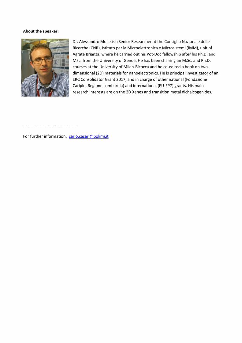
Dr. Alessandro Molle is a Senior Researcher at the Consiglio Nazionale delle
Ricerche (CNR), Istituto per la Microelettronica e Microsistemi (IMM), unit of
Agrate Brianza, where he carried out his Pot-Doc fellowship after his Ph.D. and
MSc. from the University of Genoa. He has been chairing an M.Sc. and Ph.D.
courses at the University of Milan-Bicocca and he co-edited a book on two-
dimensional (2D) materials for nanoelectronics. He is principal investigator of an
ERC Consolidator Grant 2017, and in charge of other national (Fondazione
Cariplo, Regione Lombardia) and international (EU-FP7) grants. His main
research interests are on the 2D Xenes and transition metal dichalcogenides.
------------------------------------
For further information: [email protected]

NanoLab Talk
Tuesday, 2nd october, 2018 – 11.30 Seminar Room 1° floor
Department of Energy – Cesnef (Building 19) via Ponzio 34/3 Milan Politecnico di Milano
“Measuring thin films mass thickness through
energy dispersive x-ray spectroscopy”
Andrea Pazzaglia
NanoLab – Department of Energy Politecnico di Milano
Abstract: Thin films mass thickness measurements through Energy Dispersive X-Rays Sprectroscopy (EDS), also kwown as quantitative Electron Probe Microanalysis (EPMA), was proposed for the first time in 1960 by Sweeney, Seebold and Birks [1], and it is of a great appeal thanks to its non-destructivity, the use of a common apparatus (a scanning electron microscope with an x-ray spectrometer) and its high spatial resolution down to tens of nanometers. This technique was developed till now by many authors [2], but it never reached the reliability of other standard techniques because of its several limitations: the difficulty in accurately predicting the number of X-rays generated in depth; the need of a reference sample with the same composition of the film or the substrate; the requirement of many measurements with different accelerating voltages. A new method is here presented [3], which allows to overcome all these problems thanks to the significant improvement in the modelization of electron-sample interaction. The model is based on the numerical solution of the electron transport equation in a known multilayer geometry, which allows to precisely simulate the number of the emitted characteristic X-rays in the sample. Thus, it is possible to relate, using an iterative algorithm, the ratio of X-rays number of the film over the substrate, to the film mass thickness and the composition, without the need of a reference sample and multiple voltage measurements. The model is implemented with the most recent findings in the physics of medium energy electrons interaction with solids and it is validated with benchmarks measured with a standard technique (X-Ray Reflectometry); the model accuracy is also tested with a sensitivity analysis which highlights that mass thickness measurements has a relative error lower than 10%, which is comparable to common values measured by other standard techniques. In addition, the new method also enables to exploit the EDS capability of measuring X-rays maps, in order to retrieve 2D mass thickness and composition profiles, with under-micrometer spatial resolution.

References [1] Sweeney Jr, W. E., R. E. Seebold, and L. S. Birks. "Electron probe measurements of evaporated metal films." Journal of Applied Physics 31.6 (1960): 1061-1064. [2] Pouchou, J.. "X-ray microanalysis of stratified specimens." Analytica chimica acta 283.1 (1993): 81-97. Llovet, X., and C. Merlet. "Electron probe microanalysis of thin films and multilayers using the computer program XFILM." Microscopy and Microanalysis 16.1 (2010): 21-32. Prencipe, I., et al. "Energy dispersive x-ray spectroscopy for nanostructured thin film density evaluation." Science and technology of advanced materials 16.2 (2015): 025007. [3] Pazzaglia A. et al. In preparation.
------------------------------------
For further information: [email protected] ; [email protected]
About the speaker:
Andrea Pazzaglia was born in 1991 in Milano, Italy. He is a PhD student in Energy and Nuclear Science and
Technology at Politecnico di Milano since 2016. He received his Master’s degree in Nuclear Engineering
from Politecnico di Milano with a thesis on production and characterization of nanostructured films for
laser driven ion acceleration. He is mainly interested in production, modeling and characterization of
materials for ion acceleration purposes.

NanoLab Talk Tuesday, 16th october, 2018 – 11.30
Seminar Room 1° floor Department of Energy – Cesnef (Building 19) via Ponzio 34/3 Milan
Politecnico di Milano
“The solid-liquid interface and nanomicroscopy
(solinano) lab: current activities of the new inter-
departmental facility”
Gianlorenzo Bussetti
Department of Physics , Politecnico di Milano Abstract:
A fruitful collaboration between the Energy, Physics and Chemistry Departments gave the possibility to
open the Solid-Liquid Interface and Nanomicroscopy (SoLINano) lab, which is an inter-Departmental facility
of the Politecnico di Milano. SoLINano lab is equipped with both scanning tunneling and atomic force
microscopy (STM and AFM, respectively) that can work immersed inside a liquid. When STM and AFM are
coupled with an electrochemical cell (EC-STM, EC-AFM), samples can be studied during electrochemical
processes induced by applying specific potentials to the samples. The target of these microscopies is to
explore the morphological evolution of surfaces in more realistic conditions with respect to vacuum
environments.
During its first 3-years of activity, SoLINano lab has focused the research to problems related to lead-acid
batteries. Here, in fact, graphite electrodes are exposed to diluted sulphuric acid media, which induces a
progressive detriment of the electrode. Graphite dissolution in acid environments and a possible strategy
for its protection is the main topic of the talk. Some perspectives of the next SoLINano activities will be
outlined.

About the speaker:
Gianlorenzo Bussetti (GB) followed the Master of Science in Physics at the University of Rome Tor
Vergata. His thesis work, entitled "Measurements of Anisotropy in Surface Reflectance Infrared (IR-RAS) on
the optical-transition of dangling bonds in Si (111) electron-phonon interaction and 2x1 as a function of
temperature", was held under the supervision of Em. Prof. G. Chiarotti. GB succeeded his PhD thesis with a
study on the optical properties of organic films ("Thin and ultra-thin organic layers investigated by
Reflectance Anisotropy Spectroscopy"). The results and their applications in the field of solid state devices
(namely gas sensors) have allowed GB to win the Giulotto prize and to be called by the Institute des
Nanosciences de Paris (Paris-INSP-France) and the J. Kepler University of Linz (Austria). In 2009, GB spent
some months in the team of Prof. K. Wandelt in Bonn, where he started to work with a home-made EC-
STM.
------------------------------------
For further information: [email protected]

NanoLab Talk Tuesday, 23rd october, 2018 – 11.30
Seminar Room 1° floor Department of Energy – Cesnef (Building 19) via Ponzio 34/3 Milan
Politecnico di Milano
“Novel thin film metallic glasses with unique
mechanical properties”
Matteo Ghidelli
Micro- and Nanostructured Materials Laboratory (NanoLab), Department of Energy, Politecnico di Milano, via Ponzio 34/3, 20133, Milano, Italy.
Abstract: The mechanical properties of sub-micrometer scale thin films are object of intense research aimed to develop films with high strength, hardness, and ductility. The scientific challenges cover both the synthesis and characterization. For instance, the mechanical properties are controlled by the intrinsic size of the specimen (size effects) as well as by film microstructure/atomic arrangement, while cutting-edge nano-manipulation techniques are requested for their extraction. In this context, I will cover several aspects of the synthesis and the mechanical behavior of thin film metallic glasses (TFMGs), representing an emerging materials class. In the first part of the talk, I will discuss the thickness-dependent mechanical properties (size effects) for Zr65Ni35 (%at.) TFMGs on a substrate and freestanding. I will show that TFMGs with different thickness have similar atomic structure, while reporting a change on hardness and of the failure mechanisms. Then, I will discuss mechanical size effects for freestanding TFMGs investigated using an innovative method based on residual stress actuated microtensile set-up. I will show that TFMGs can sustain large homogenous deformation (~15%) without catastrophic shear banding, while the yield strength reaches the theoretical limit of ~3000 MPa. I will discuss the fundamental plasticity mechanisms presenting the results of high-resolution TEM and nanobeam electron diffraction. I will show that TFMGs reports a fine glassy nanostructure with a well-defined dense Ni-rich clusters embedded in Zr-rich clusters with lower atomic density and a characteristic length scale of ~2-3 nm. Moreover, I will show that plastic deformation correlates with continuously homogenous disruption of the local atomic order. In the second part of the talk, I will present recent results related with the synthesis of advanced nanostructured Zr50Cu50 (%at.) TFMGs by Pulsed Laser Deposition (PLD). I will show how PLD can be used to synthetize a variety of metallic film microstructures including compact fully amorphous, amorphous nano-porous, and amorphous films embedded with nanocrystals. I will show that as-deposited TFMGs are characterized by a unique nano-laminated atomic structure and I will discuss the effect of annealing treatments to induce a partial crystallization. Finally, I will present selected nano-mechanical results discussing the trend of hardness, elastic modulus, and thermal stability for different film morphologies

About the speaker:
Dr. Matteo Ghidelli received a master degree in materials
engineering (summa cum laude) from both Politecnico di Milano
and Torino. In 2015, he completed a joint PhD between the
Université Grenoble Alples (France) and the Université catholique
de Louvain (Belgium) within the framework of the International
Doctoral School in Functional Materials (IDS-FunMat). After one-
year post-doc experience at the Università Roma Tre, he got a
second post-doc position at Politecnico di Milano winning a Polimi
International Fellowship (PIF). He has recently been appointed
Group Leader (assistant professor) at the Max-Planck-Institut für
Eisenforschung (MPIE, Düsseldorf) where he will lead the group of
“Synthesis of Nanostructured Materials”.
His main research interests involve the synthesis of
nanostructured thin films and the study of their mechanical/functional properties. He is author of 16
publications (h-index 12) in high impact factor journals.
------------------------------------
For further information: [email protected]
NanoLab Talk Monday, 29th october, 2018 – 15.30
Seminar Room 1° floor Department of Energy – Cesnef (Building 19) via Ponzio 34/3 Milan
Politecnico di Milano
“Modelling Oxide Surfaces at the 2D Limit”
Sergio Tosoni
Dipartimento di Scienza dei Materiali, Università di Milano - Bicocca Abstract: In this seminar, the role of first-principles simulations in elucidating structural properties and chemical reactivity of metal-supported oxide thin films will be discussed. Thin oxide films supported on metals represent an interesting class of materials for many applications, spanning from microelectronics to heterogeneous catalysis. From the chemist’s perspective, the most relevant aspect of these systems is perhaps the spontaneous charge transfer taking place at the metal/oxide interface, which strongly influences the adsorptive properties and reactivity at the oxide surface. Computer simulations can achieve a reliable description of the structural details and charge state of adsorbed species on oxide thin films, relating the oxide/support interplay to the surface chemical activity. This was first seen in the case of gold single atoms and small clusters adsorbed on a simple model system of metal-supported ionic oxide, namely Ag- or Mo-supported MgO.[1] Interestingly, similar effects have been recently observed also in the case of a real catalyst employed in industrial catalytic synthesis of methanol, namely a ZnO bilayer supported on Cu.[2] However, there are critical aspects to be considered when simulating complex metal-oxide interfaces. On the one hand, calculations on these systems are often computationally demanding, due to the large dimension of the supercells required to reduce the strain arising from the metal/oxide lattice mismatch. On the other hand, it is not trivial to find a computational method describing equally well the metallic and the oxidic parts of the interface and still being efficient enough to treat large systems. References
[1] Ricci et al., Phys. Rev. Lett. 2006, 97, 036106−4. [2] Thang et al., ACS Catal. 2018, 8, 4110.

About the speaker:
Dr. Sergio Tosoni is a research associate at the Materials Science Department,
University of Milano - Bicocca. He received his PhD in Chemistry at the
University of Torino in 2007. He then held Postdoc positions at the Humboldt
University, Berlin, and the University of Barcelona. His main research interests
concern first-principles simulations of catalytic and photocatalytic properties of
oxide surfaces, metal-oxide interfaces, adsorption and weak interactions.
------------------------------------
For further information: [email protected]

NanoLab Talk Tuesday, 13th october, 2018 – 11.30
Seminar Room 1° floor Department of Energy – Cesnef (Building 19) via Ponzio 34/3 Milan
Politecnico di Milano
“Cumulenes and polyynes as carbon atomic wires”
Rik Tykwinski
University of Alberta, Edmonton Alberta Canada Abstract:
Oligoynes, polyynes, and cumulenes (constructed of sp-hybridized carbon, known as carbon atomic wires – CAWs) are arguably the simplest molecular wires. In addition to their and semi-rigid structure, electronic delocalization through the conjugated framework is essentially unaffected by bond rotation, which separates CAWs from nearly all other wire motifs. While shorter CAWs are reasonable stable and easy to study, longer CAWs are often chemically unstable, which renders them inefficient for device formation. Thus, the development of synthetic routes that provide stable molecules for incorporation into devices is necessary in order to answer questions related to the performance of CAWs.
Our recent work has targeted three major challenges regarding CAWs, including 1) The synthesis of polyyne[1] and cumulene[2] CAWs to model carbyne (the sp-hybridized carbon allotrope), 2) The study of structural aspects of CAWs, and 3) Synthetic approaches to stabilize CAWs for devices.[3] For example, pyridyl endgroups have been designed with sterically demanding substituents that protect the CAWs, while maintaining access of the pyridyl nitrogen to the electrodes. Alternative, we use supramolecular chemistry to form rotaxanes in which the linear polyyne is threaded through a macrocycle, forming the equivalent of an insulated molecular wire. Third, we use the pyridyl nitrogen to coordinate to transition metals, which provides alternative structures for molecular wires. The use of CAWs in single molecule devices ultimately helps to provide an answer to the question of performance based on structure and length.
Figure 1. Examples of pyridyl endcapped CAWs for devices.
References
[1] W.A. Chalifoux, R.R. Tykwinski, Nat. Chem. 2010, 2, 967–971.
[2] J.A. Januszewski, R.R. Tykwinski, Chem. Soc. Rev. 2014, 43, 3184–3203.
[3] D.C. Milan, M. Krempe, A.K. Ismael, L.D. Movsisyan, M. Franz, I. Grace, R.J. Brooke, W. Schwarzacher,
S.J. Higgins, H.L. Anderson, C.J. Lambert, R.R. Tykwinski, R.J. Nichols, Nanoscale 2017, 9, 355–361.

About the speaker:
Rik R. Tykwinski earned his BS at the University of Minnesota – Duluth (1987) and his PhD the University of Utah with Professor Peter Stang (1994). As a PDF at ETH-Zurich, he worked with Professor François Diederich, and in 1997 he joined the faculty at the University of Alberta. In 2009, he moved to Germany to accept the position of Chair of Organic Chemistry at the University of Erlangen-Nurnberg, and in 2016 he moved back to Alberta as Chair of the Department of Chemistry. He is a physical organic chemist, with a focus on structure-property relationships in conjugated molecules, especially polyynes and cumulenes. In his free time, he enjoys mountain biking and entertaining his sons.
------------------------------------
For further information: [email protected]

NanoLab Talk Tuesday, 27 th october, 2018 – 11:30
Seminar Room 1° floorDepartment of Energy – Cesnef (Building 19) via Ponzio 34/3 Milan
Politecnico di Milano
Superintense laser interaction with nanostructuredtargets.
Luca Fedeli
Department of Energy, Politecnico di Milano, ItalyAbstract:
Thanks to Chirped Pulse Amplification[1] (for which the Nobel Prize in Physics was awarded in 2018),state-of-the art laser systems can now reach extremely high intensities, exceeding 10 22 W/cm2 [2]. For thetypical wavelength of these systems (~ 1 μm), intensities above ~ 1018 W/cm2 are high enough to accelerateelectrons up to relativistic energies in a single laser cycle. This marks the threshold for the so-called“relativistic regime” of laser-matter interaction. These field intensities being much greater than the typicalatomic fields, in this regime any kind of material rapidly becomes a plasma.
Relativistic laser-plasma interaction has been explored extensively In the last decades,for applications including particle[3,4] and secondary photons sources[5], inertialconfinement fusion[6] and probing QED processes[7].
This contribution will be focused on advanced laser-driven ion sources, based on ultra-intense laser interaction with foils coated with a nanostructured low-densityfoam[8,9,10,11]. In this scheme, the laser is efficienlty absorbed in the low-density layer,generating electrons at MeV energies. The expansion of this hot electrons cloud leads tothe formation of an intense electric field at the back side of the foil. This field isresponsible for the ion acceleration process. Table-top lasers could be used to
accelerate ions at few MeVs energies, which is attractive for several applications[12,13]. Particularattention will be given to numerical simulations of ultra-intense laser interaction with low-densitynanostructured materials[14], which are important to elucidate the physical processes at play.
References:
[1]D. Strickland et al. Opt. Commun. 55(6), 447-449 (1985)
[2]C. Danson et al. High Power Laser Sci. Eng. 3 (2015)
[3]A.Macchi et al. Rev.Mod.Phys. 85, 751 (2013)
[4]E.Esarey et al. Rev.Mod.Phys. 81, 1229 (2009)
[5]G.Sarri et al. Phys. Rev. Lett. 113, 224801 (2014)
[6]R. Betti et al. Nat. Phys. 12, 435-448(2016)
[7]A.Di Piazza et al. Rev.Mod.Phys. 84, 1177 (2012)
[8]A.Sgattoni et al. Phys.Rev. E 85, 036405 (2012)
[9]I.Prencipe et al. Plasma Phys. Control. Fusion 58,3 (2016)
[10]M.Passoni et al. Phys.Rev.Accel.Beams 19, 061301 (2016)
[11] A. Zani et al. Carbon 56, 358-365 (2013)
[12]F.Mirani. Master’s thesis. Politecnico di Milano (2017)
[13]M.Passoni et al. Under review at Sci.Rep. (2018)
[14]L. Fedeli et al. Sci. Rep. 8, 3834 (2018)
ERC-2014-CoG No.647554ENSURE
About the speaker:
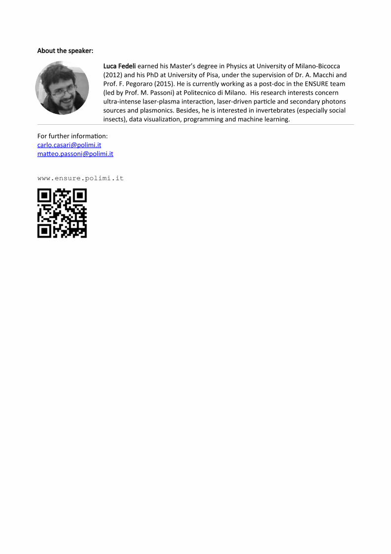
Luca Fedeli earned his Master’s degree in Physics at University of Milano-Bicocca (2012) and his PhD at University of Pisa, under the supervision of Dr. A. Macchi and Prof. F. Pegoraro (2015). He is currently working as a post-doc in the ENSURE team (led by Prof. M. Passoni) at Politecnico di Milano. His research interests concern ultra-intense laser-plasma interaction, laser-driven particle and secondary photons sources and plasmonics. Besides, he is interested in invertebrates (especially social insects), data visualization, programming and machine learning.
For further information: carlo.casari @polimi.it matteo.passoni @polimi.it
www.ensure.polimi.it

NanoLab Talk Tuesday, 22nd January, 2019 – 11.30
Seminar Room 1° floor Department of Energy – Cesnef (Building 19) via Ponzio 34/3 Milan
Politecnico di Milano
“Hyperspectral Imaging and Microscopy”
Cristian Manzoni
Istituto di Fotonica e Nanotecnologie – CNR Dipartimento di Fisica, Politecnico di Milano, Piazza Leonardo
da Vinci 32, I-20133 Milano, Italy
Abstract:
Spectral imaging, also known as imaging spectroscopy, refers to methods and devices for acquiring a complete light spectrum for each point in the image of a scene. It provides much richer information with respect to standard imaging, enabling to identify materials or detect dynamical processes. Spectral imaging has been applied to a wide range of scientific investigations, such as remote sensing, pigment determination in biology, medicine, coastal ocean imaging, water analysis, agriculture, cultural heritage and archaeology, just to cite a few. In particular, hyperspectral imaging aims at acquiring the whole continuous spectrum of each point of the scene. A powerful approach to this aim is to combine classical imaging with Fourier-transform spectrometry [1]. In this talk, I will describe the main properties of the spectral imaging and the current acquisition approaches. I will also show the most recent advancements obtained at the Istituto di Fotonica e Nanotecnologie (IFN-CNR), based on an innovative optical device [2]. Our compact hyperspectral system is able to acquire spectral reflectance and fluorescence images with high sensitivity, broad spectral coverage and high spectral resolution. Examples of hyperspectral remote-sensing and microscopy images will be provided and discussed.

Hyperspectral imaging of an Egyptian cartonnage. (a) RGB image synthesized from the hyperspectral data; (b) False color fluorescence image after illumination at λ = 617 nm; fluorescence arises from a dye known as Egyptian Blue (CaCuSi4O10) [3]. (c) Solid/dashed lines: Reflectance spectra of three points of panel (a); shaded area: fluorescence spectrum of light areas of panel (b).
References
[1] S.P. Davis, M.C. Abrams, and J.W. Brault, Fourier Transform Spectrometry (Academic Press, 2001)
[2] D. Brida, C. Manzoni, and G. Cerullo, “Phase-locked pulses for two-dimensional spectroscopy by a birefringent delay line,” Opt. Lett. 37, 3027-3029 (2012)
[3] D. Comelli, V. Capogrosso, C. Orsenigo, and A. Nevin, “Dual wavelength excitation for the time-resolved photoluminescence imaging of painted ancient Egyptian objects”, Heritage Science 4, 1-8 (2016)
About the speaker:
Cristian Manzoni received his PhD in Physics at the Physics Department of Politecnico di Milano. From 2006 to 2009 he was Post Doc at the same institution. In 2009 he joined as Post Doc the Max Planck Research Group for Structural Dynamics at CFEL (Hamburg, Germany), where he devoted to time resolved spectroscopy on high-temperature semiconductors in the mid-infrared and THz spectral range. Since 2010 he is researcher at the Institute of Photonics and Nanotechnology of the National Research Council of Italy. His main scientific activity focuses on the synthesis of few-optical-cycle laser pulses and on their application to time-resolved spectroscopy and nonlinear processes. He is currently developing hyperspectral imaging based on the Fourier transform approach. He is co-author of 90 peer-reviewed papers, 4 book chapters on ultrabroadband nonlinear optics and spectroscopy, and more than 130 contributions to international conferences. He holds 1 international patent.
------------------------------------
For further information: [email protected]

NanoLab Talk Tuesday, 5th february, 2019 – 11.30
Seminar Room 1° floor
Department of Energy – Cesnef (Building 19) via Ponzio 34/3 Milan Politecnico di Milano
“Determination of the ion temperature in a high-
energy-density plasma using Stark effect”
Yitzhak Maron
Faculty of Physics, Weizmann Institute of Science, Rehovot 7610001, Israel Abstract:
We present experimental determination of the ion temperature in a neon-puff Z-pinch. The diagnostic method is based on the effect of ion coupling on the Stark line shapes. Discussed will be the spectroscopic measurements required and the data analysis. It was found that at stagnation the ion thermal energy is small compared to the imploding-plasma kinetic energy, where most of the latter is converted to hydro motion. The method here described can be applied to other highly non-uniform and transient high-energy-density plasmas, where realization of the previous approach developed (Kroupp et al, PRL, 2011) is unfeasible.

About the speaker:
Yitzhak Maron is Professor, Weizmann Institute of Science and Head of the Plasma Laboratory, Faculty of Physics, Weizmann Institute of Science, Rehovot 76100, Israel. E-mail: [email protected]. His research activities regard: Plasma Physics, Atomic Physics, Plasma Spectroscopy, Non-Equilibrium High Energy Density Physics, Plasmas Under Pulsed Magnetic Fields, Plasma Implosion and Stagnation, Laser-Matter interaction, Warm-Dense Matter, Implications to Fusion and Space Physics. He is in the Editorial Board of Laser and Particle Beams (2005) and of Matter and Radiation at Extremes
------------------------------------
For further information: [email protected]; [email protected]

NanoLab Talk Tuesday, 12th February, 2019 – 11.30
Seminar Room 1° floor Department of Energy – Cesnef (Building 19) via Ponzio 34/3 Milan
Politecnico di Milano
“Micro Spatially Offset Raman Spectroscopy for the investigation of materials subsurface”
Claudia Conti
Istituto per la Conservazione e la Valorizzazione dei Beni Culturali, CNR, Milano
Abstract:
One of major outstanding and only partially addressed needs in the conservation and material sciences is the non-destructive and non-invasive analysis of subsurface components with molecular specificity at micrometre scales. This capability is just in part fulfilled by confocal Raman microscopy, since its depth‐resolving power is restricted to depths at which sample is transparent or semi‐transparent. In case of highly diffusely scattering layers, i.e. painted stratigraphies, the restriction can be very severe and, although it is highly undesirable and, in many cases, impossible with precious objects of art, cross section sampling becomes the only available recourse.
Micro Spatially Offset Raman Spectroscopy (micro-SORS), a recently developed approach for non‐destructive probing in turbid media[1-3] combines conventional SORS[4] with microscopy concepts and represents a new imaging modality in Raman microscopy. It provides analytical capability for investigating non-invasively the chemical composition of subsurface, micrometer scale-thick diffusely scattering layers at depths more than an order of magnitude larger than those accessible with conventional confocal Raman microscopy[5]. The method involves separating the laser illumination and Raman collection zones from each other on sample surface to facilitate deeper recovery of sublayer signals and identify their chemical makeup.
Figure 1. Example of micro-SORS experiment.

References
[1] C. Conti, C. Colombo, M. Realini, G. Zerbi, P. Matousek, Appl. Spectrosc. 2014, 68, 686. [2] C. Conti, M. Realini, C. Colombo, K. Sowoidnich, N.K. Afseth, M. Bertasa, A. Botteon, P. Matousek, Anal. Chem. 2015, 87, 5810. [3] C. Conti, A. Botteon, M. Realini, C. Colombo, P. Matousek, Anal. Chem. 2017, 89, 11476. [4] P. Matousek, I. P. Clark, E. R. C. Draper, M. D. Morris, A. E. Goodship, N. Everall, M. Towrie, W. F. Finney, A. W. Parker, Appl. Spectrosc. 2005, 59, 393.
[5] C. Conti, C. Colombo, M. Realini, P. Matousek, J. Raman Spectrosc. 2015, 46, 476.
About the speaker:
Claudia Conti, researcher at the Institute for the Conservation and Valorization of Cultural Heritage (ICVBC) of the National Research Council (CNR), obtained her PhD degree in Materials Engineering from the Milan Polytechnic in 2010. Through her PhD and research at ICVBC she established an expertise in the area of advanced applications of vibrational spectroscopy to the analysis of materials, in particular in Cultural Heritage. She supervises the Raman Laboratory at ICVBC, started by her after PhD. In 2014 and in 2018 she was a visiting scientist at the STFC Rutherford Appleton Laboratory (UK), under CNR’s Short Term Mobility programs, where she developed a new Raman method (micro-SORS) for the non-invasive analysis of micrometric turbid layers.
------------------------------------
For further information: [email protected]
NanoLab Talk Tuesday, 19th February, 2019 – 11.30
Seminar Room 1° floor Department of Energy – Cesnef (Building 19) via Ponzio 34/3 Milan
Politecnico di Milano
“Synchrotron-radiation for the investigation of free
nanoparticles in a molecular beam”
Paolo Piseri
Dipartimento di Fisica, Università degli Studi di Milano Abstract: The use of nanoparticles as building-blocks for the assembly of thin-films and layered systems has been proposed as a paradigm for a bottom-up approach to nanostructured materials and interfaces with novel functional properties. Despite the directness of this argument, the demonstration of a direct connection between assembled system properties and those owned by their elementary constituents is far from being assessed. The hurdle is enhanced by the relevant fact that the novel properties of interest are often emerging after the assembly and not merely inherited from the building blocks, still the current capacity of measuring chemical and physical properties of truly isolated nanoparticles is very limited and far from being able to provide a solid ground on which the bottom-up paradigm can be discussed, possibly assessed and further developed in its full complexity. Core-level spectroscopy techniques are well-established methods with remarkable power for the investigation of condensed matter and gas-phase molecular systems. The ability to routinely apply similar methods to free and isolated nanoparticles would definitely provide a valuable contribution to the scientific and technological challenge of bottom-up nanofabrication. Since over one decade we have been developing experiments and dedicated instrumentation for synchrotron-radiation –based investigation of free clusters and nanoparticles [1]. The seminar will present selected examples from this activity with the aim of discussing current directions, state of the art and future perspectives. References
[1] P. Piseri et al., J Elec Spectrosc Relat Phenom 166-167, 28 (2008).

About the speaker:
Paolo Piseri is associate professor at the Physics Department, University of Milano. He is
graduate and PhD laureate in Physics from the same university (years 1995 and 2000). In year
2004 he co-founded the company Tethis (as a spin-off of UNIMI and INFM), which is now
independent and active in the industrial exploitation of nanostructured materials for
biomedical applications.
His main research interest is the development of novel methods for nanoparticle production, manipulation
and characterization in the gas-phase. Since 2003 he devotes part of his efforts to the exploitation of
synchrotron radiation and free electron laser light sources for the investigation free nanoparticles in
molecular beams.
------------------------------------
For further information: [email protected]
For further information please contact: [email protected]
NanoLab Talk
Politecnico di Milano, Department of Energy, Cesnef (Building 19), via Ponzio 34/3, Milan
Seminar Room 1° floor
Tuesday, 12th March, 2019 – 14.00
Non-equilibrium Photophysics of Layered Two-
dimensional Semiconductors and their Heterostructures
Christoph Gadermaier
Dipartimento di Fisica, Politecnico di Milano Two-dimensional semiconductors combine easy fabrication and mechanical flexibility with particularly strong light-matter interaction. The absorption spectra of 2D semiconductors are dominated by excitons with binding energy up to several hundred meV. Yet, even single layers show some degree of charge carrier photogeneration. Using femtosecond optical pump-probe spectroscopy we show that in few-layer MoS2, the hot electron-hole pairs created by photoexcitation relax and form free carriers within 700 fs [1]. In monolayers, the relaxing hot carriers form a mixed population of excitons and free carrier pairs. A moderate in-plane electric field of a few kVcm-1 can significantly change the branching ratio in favour of free carrier pairs [2]. The fate of photogenerated carriers is trapping at defects, with a much higher defect content for thicker flakes [3]. At higher fluencies, once the defects are saturated, carriers mostly recombine non-geminately. Van der Waals heterostructures (HS), obtained by stacking two different monolayers on each other, have been intensively investigated because of their possible applications in optoelectronics and light harvesting. Type II HS, where the valence band maximum and the conduction band minimum are in separate layers, allow efficient charge separation, which is particularly beneficial for photovoltaics based on atomically thin materials. In a type II WSe2/MoSe2 HS we observe a fast interlayer hole transfer occurring in less than 1 ps, which can be clearly time-resolved in our experiment. The hole transfer yields an interlayer exciton (i.e. a bound state of an electron and a hole residing in two separate layers) [4].
References
[1] T. Borzda et al., Adv. Funct. Mater. 25, 3351 (2015).
[2] D. Vella et al., 2d Mater. 4, 035017 (2017).
[3] V. Vega-Mayoral et al., 2d Mater. 5, 015011 (2018).
[4] Z. Wang et al., in preparation.
About the speaker:
Christoph Gadermaier is Associate Professor at the Physics Department, Politecnico di Milano. He graduated
in Technical Physics at Graz University of Technology (Austria) in 1999 and obtained his PhD there in 2002.
His research focusses on the electron dynamics in solids, with a particular emphasis on the processes that
occur on the fs time scale. Over the course of his career, he has investigated a wide range of materials, most
notably conjugated polymers and oligomers, carbon nanotubes, inorganic nanowires, high-temperature
superconductors, and two-dimensional layered semiconducting transition metal dichalcogenides.
I have beams.

For further information please contact: [email protected]
NanoLab Talk
Politecnico di Milano, Department of Energy, Cesnef (Building 19), via Ponzio 34/3, Milan
Seminar Room 1° floor
Monday, 18th March, 2019 – 14:30
Nuclear Measurements Group @ PoliMi:
recent developments and open questions
Andrea Pola Dipartimento di Energia, Politecnico di Milano
The Nuclear Measurements Group of Politecnico di Milano focuses its activity on the feasibility study and development of novel detection techniques and systems. Main fields of interest are the nano-microdosimetry of therapeutic hadron beams, the neutron spectrometry (low and high resolution) from thermal energies to GeV and the characterization of novel particle fields for medical applications. Different recent developments have highlighted new questions and needs more directly related to material science and nanotechnology. The design of a new gas detector able to characterize ionization distribution induced by heavy reaction products at the nanoscale have raised questions about the design and construction of the overall system [1]. The development of a new neutron spectrometer based on thermal neutron sensors triggered the need of studying an effective alternative method of device functionalization [2]. Eventually, the need for studying the physics of reactions induced by protons on boron and fluorine introduces the necessity of producing thin converters to be coupled to active detectors [3].
References
[1] D. Bortot et al., Radiation Measurements 103 (2017), 1-12
[2] A. Pola et al, Radiation Protection and Dosimetry 161 (2014), 229-232
[3] G.A.P. Cirrone et al., Nature Communications, Scientific Reports 8, 1141 (2018)
About the speaker:
Andrea Pola is associate professor in the field of Nuclear Instrumentation and
Measurements. He is graduate in Nuclear Engineering and PhD in Radiation Science
and Technology at Politecnico di Milano (years 2002 and 2006) and he presently
works at the Department of Energy of Politecnico di Milano. His research is mainly
devoted to the development of novel detection systems for radiation physics,
especially for neutron spectrometry and nano-microdosimetry of charged particle
beams. He is responsible for the Neutron Metrology Facility of Politecnico di Milano.

For further information please contact: [email protected]
NanoLab Talk
Politecnico di Milano, Classroom C.I.1 (Building 6)
Thursday, 28th March, 2019 – 14:00
Light Scattering and Emission from Hetero-structures
Andrea Carlo Ferrari Cambridge Graphene Centre, University of Cambridge, Cambridge, CB3 OFA, UK
Heterostructures based on layers of atomic crystals have a number of properties often unique and very
different from those of their individual constituents and of their three dimensional counterparts. The
combinations of such crystals in stacks can be used to design the functionalities of such heterostructures. I
will show how Raman spectroscopy can be used to fingerprint such heterostructures, and how these can be
exploited in novel light emitting devices, such as single photon emitters, and tuneable light emitting diodes.
About the speaker:
Andrea Ferrari is Professor of nanotechnology at the University of Cambridge
and a Fellow of Pembroke College. He graduated in Nuclear Engineering at
Politecnico di MiIano. He founded and directs the Cambridge Graphene
Centre and the Engineering and Physical Sciences Research Council Doctoral
Training Centre in Graphene Technology. He chairs the management panel
and is the Science and Technology Officer of the 1Billion Euros European
Graphene Flagship. He is a Fellow of the American Physical Society, Fellow of
the Materials Research Society, Fellow of the Institute of Physics, Fellow of
the Optical Society and he has been recipient of numerous awards, such as
the Royal Society Brian Mercer Award for Innovation, the Royal Society Wolfson Research Merit Award, the
Marie Curie Excellence Award, the Philip Leverhulme Prize, The EU-40 Materials Prize. He has also received
5 European Research Council Grants. He is the "Top Italian Scientist in Material & Nano Sciences" according
to the VIA-Academy rankings. He has over 370 papers with over 96,000 citations, with an H index of 105.

For further information please contact: [email protected]
NanoLab Talk
Politecnico di Milano, Department of Energy, Cesnef (Building 19), via Ponzio 34/3, Milan
Seminar Room 1° floor
Monday, 8th April, 2019 – 14.30
Recent developments in Non-Evaporable Getter
technology and application in vacuum systems from HV to
XHV
Fabrizio Siviero
SAES Getters S.p.A. Non-Evaporable Getter (NEG) pumps are able to efficiently absorb chemically reactive gases by binding them on their active surface. They find application in a large variety of UHV-XHV systems like analytic instruments (SEM, TEM, surface science and semiconductor industry tools), cold atomic traps, portable spectrometers and particle accelerators. The key strengths of NEG pumps are:
- the very high pumping speed, in particular for hydrogen, oxygen and water; - the compactness, both in terms of size and weight; - the absence of moving parts, i.e. vibrations; - the ability to work at RT in absence of power.
During the last ten years two major innovations have been introduced, which expanded significantly the range of application of NEG materials. On one side, the integration of Sputter Ion Pump (SIP) and NEG technology allowed to approach the design of vacuum systems in a radically new and more efficient way [1]. Then, the development of the ZAO® alloy (ZrVTiAl) and new production processes of sintered porous pumping elements, opened the way to the use of NEG pumps in the HV pressure range (10-8 – 10-7 mbar), where a much larger capacity than UHV getter solutions is required. The seminar will present the basic properties of NEG materials and selected examples of their application in small and large vacuum systems of scientific interest [2].
References
[1] P. Manini et al., Vacuum 94, 26 (2013).
[2] F. Siviero et al., Fusion Engineering and Design (2019), DOI 10.1016/j.fusengdes.2019.03.026
About the speaker:
Fabrizio Siviero works in the R&D labs of SAES Getters, as part of the Vacuum Systems Business Unit. He
graduated in physics from the Università degli Studi di Milano in 2000 and took a PhD in the same university
in 2003. Then, he had post-doctorate experiences at CNR in Trento and at the Politecnico di Milano. His
research focused on the deposition and characterization of nanostructured thin films with several surface
science techniques. In 2008 he joined SAES , where he is involved in the development of Non-Evaporable
Getter (NEG) materials and NEG pumps, as well as their functional characterization. Part of his activity is
related to the analysis of vacuum systems, from the lab scale up to large machines like particle accelerators
and nuclear fusion experiments.

For further information please contact: [email protected]
NanoLab Talk
Politecnico di Milano, Department of Energy, Cesnef (Building 19), via Ponzio 34/3, Milan
Seminar Room 1° floor
Monday, 6th May, 2019 – 14.30
Teaching quantum physics in high school: a low-cost
experimental approach
Paolo Gondoni Istituto di Istruzione Superiore “S. ten. Vasc. A. Badoni” - Lecco
Since the latest reforms in the Italian secondary education system, teachers are required to deal with some
aspects of XXth century physics in the final year of scientific high school, which is the source of most
students enrolling at Politecnico. Especially with the new system of final examinations, students must be
able to solve and discuss simple problems involving special relativity and quantum mechanics.
While introducing QM without relying on an adequate mathematical basis is a serious challenge, some
interesting approaches have been developed in order to provide, where possible, an experimental point of
view. Even with the extremely low budget available in school labs, some simple experiments can be
performed which allow to familiarize with one of the staples of QM, i.e. Planck’s constant.
In this talk, a series of experiments developed by prof. I. Cormio [1] will be presented, which lead to an
experimental measurement of h by studying the emission spectra of different-colored LEDs and comparing
them with a simplified energy balance for electrons traversing the junction, based on I-V measurements
carried out on lab breadboards.
Disclaimer: due to the presence of some documents published by the Ministry of Education and of the
original work by prof. Cormio, who kindly asked to refrain from editing his presentation, some of the slides
will be in Italian.
References
[1] http://ls-osa.uniroma3.it
About the speaker:
Paolo Gondoni graduated at Politecnico di Milano in 2010, where he obtained his PhD at NanoLab in 2014,
working in the field of nanomaterials for photovoltaic applications. He is author of several publications on
international journals in that field, which is completely unrelated to his current activity as a high school
teacher. He has worked as a physics teacher in 5 schools in Lecco and surroundings since 2014, as a
supporting teacher in 15 courses at Politecnico since 2011, as a teacher 4 in pre-courses at Politecnico and
as 3 courses a seasonal lecturer at Università Bicocca between 2013 and 2015.

For further information please contact: [email protected]
NanoLab Talk
Politecnico di Milano, Department of Energy, Cesnef (Building 19), via Ponzio 34/3, Milan
Seminar Room 1° floor
Monday, 20th May, 2019 – 14.30
Printed Polymer Electronics
Mario Caironi Center for Nano Science and Technology @PoliMi, Istituto Italiano di Tecnologia, Milano, Italy
Polymer semiconductors with steadily improved electronic properties
are being synthesized, achieving charge mobility in excess of 5 cm2/Vs
for electrons and holes. Such performances are sufficient for a large
range of applications of printed, light-weight and mechanically robust
circuits, in diverse fields such as wearable electronics, smart
packaging, and bio-electronics. I will report on recent progress in the
development of low-voltage printed circuits on plastic and in the
improvement of the operational frequencies of direct-written transistors.
Despite such progresses, charge transport properties in high mobility donor-
acceptor polymer films is still under debate. In this context, charge
modulation spectroscopy (CMS) and microscopy (CMM) allow to gather
useful information on the nexus between film microstructure and electronic
properties, and on the nature of charge carriers. CMS and CMM are
powerful tools as they can selectively probe and map carriers at the buried
semiconductor-dielectric interface in a working field-effect transistor. I will
show some examples on the use of such techniques in rationalizing
transport properties in recent high-mobility polymers.
About the speaker:
Mario Caironi obtained his Ph.D. in Information Technology at “Politecnico di Milano” with honours in 2007,
with a thesis on organic photodetectors and memory devices. In 2007 he joined the group of Prof. H.
Sirringhaus at the Cavendish Laboratory (Cambridge, UK) as a post-doctoral research associate. He worked
in Cambridge for 3 years on high resolution inkjet printing of downscaled organic transistors and logic gates,
and on charge injection and transport in high mobility polymers. In 2010 he was appointed as a Team
Leader at the Center for Nano Science and Technology@PoliMi of the Istituto Italiano di Tecnologia (Milan,
Italy), and in 2019 he became tenured senior researcher at the same institution. He is author and co-author
of more than 120 scientific papers in international journals and books. He is currently interested in solution
based high resolution printing techniques for micro-electronic, opto-electronic and thermoelectrics devices
fabrication, in the device physics of organic semiconductors based field-effect transistors and their
integration in high-frequency printed circuits, and in biomedical and/or implantable sensors and electronics
for the healthcare. He is an 2014 ERC grantee.

For further information please contact: [email protected]
NanoLab Talk
Politecnico di Milano, Department of Energy, Cesnef (Building 19), via Ponzio 34/3, Milan
Seminar Room 1° floor
Monday, 3rd June, 2019 – 14.30
Induction Assisted Laser Welding
of High Thickness Steel
Alessandro Bailini
BlueThink SpA
High thickness steel pipes for oil&gas applications are currently joined through two standard procedures:
multi-pass MAG welding or threaded joints. The first one is used for onshore and offshore pipeline
realization for oil and gas transport; the second one is employed in well completion through casing
realization for oil extraction. Both technologies are well known and reliable, but they are characterized by a
demanding preparation of pipe bevel and low process velocity.
Laser Welding is a promising technique because it could in principle overcome these problems: a high-
power laser can weld at several m/min even high thickness components (>10 mm) and it requires simple
square bevels [1]. The most important technological issue concerns the metallurgical properties of the
welded joint; the laser beam has a high power density focused in a very small region, thus the overall
thermal energy released to the material is low: the welded joint cools down rapidly and it can withstand
microstructure transition from ferrite/perlite/bainite to martensite; it can be hard and brittle, thus not
suitable for bending and torsion stresses.
The introduction of an additional thermal source can slow down the cooling speed avoiding the formation of
martensite; induction heating is a good candidate because it guarantees high energy efficiency and simple
equipment [2]. In order to keep high process velocity the induction heating system should be designed ad
hoc with respect to experimental process parameters.
In this work a combined simulation-experimental approach has been developed: starting from thermal
balance equation, laser beam propagation shape and interaction radiation-matter considerations a
simulative algorithm has been developed in Python. Simulation results have been used as input for
experimental apparatus dimensioning and prototyping. The experimental campaign was focused on low
carbon steel pipes and led to the definition of process parameters that guarantee good metallurgical
properties (analyzed using SEM microscope), good mechanical properties (tensile, bending, resilience and
hardness) and industrial scalability of the process [3] [4].
References
[1] Y. Gainand, J. P. Mas, J. P. Jansen, J. C. Coiffier, J. C. Dupont and C. Vauthier Laser orbital welding applied
to offshore pipeline construction Proceedings of 3rd International Conference on Pipeline Technology, Vol.
2, 327–342; (2000) Amsterdam, Elsevier Science BV

For further information please contact: [email protected]
NanoLab Talk
[2] A. Schneider, V. Avilov, A. Gumenyuk and M. Rethmeier, "Laser beam welding of aluminum alloys under
the influence of an electromagnetic field," Physics Procedia, vol. 41, pp. 4-11, 2013.
[3] Alessandro Bailini, Davide Rossin, Paolo Bargero, Diego Doni, Adriano Calzavara, Angelo Doni and Fabio
Freschi, Parametric Investigation on Localized Induction Heating of Thick Steel Plates, Heating by
Electromagnetic Sources Conference, HES-16 (2016) 281
[4] Davide Rossin, Giorgio Stefano, Alessandro Bailini, Erica Guerriero and Marco Franzosi, Weldability of
thick carbon steel pipes for Oil&Gas with high power density fiber laser welding; metallurgical and
mechanical properties of weld joints and applicability in offshore pipeline construction projects, Giornate
Nazionali di Saldatura – 9 (2017)
About the speaker:
Bailini Alessandro has a MSc in Nuclear Engineering and a PhD in Materials Engineering at
Politecnico of Milan; he focused his research on nano-structured materials for
thermoelectric applications.
He is author of more than 15 publications on international scientific journals and 5
patents; he has taken part in numerous national and international projects in the
development of innovative start-ups in the field of energy, utilities and industrial
processes.
He is currently shareholders and Chief Operating Officer of BlueThink SpA with the role of Project Manager
and Team Supervisor for innovation projects for technology transfer in the Oil & Gas, Energy, Utility and
Home Appliance sectors.

For further information please contact: [email protected]
NanoLab Talk
Politecnico di Milano, Department of Energy, Cesnef (Building 19), via Ponzio 34/3, Milan
Seminar Room 1° floor
Wednesday, 12th June, 2019 – 11.30
Earth-abundant Metal-metalloid Materials as Efficient
Oxygen-Evolving Electrocatalyst
Jean Marie Vianney Nsanzimana
School of Chemical and Biomedical Engineering, Nanyang Technological University, Singapore Electrochemical energy conversion and storage devices including metal-air batteries, regenerative fuel cells,
and water-splitting cells are critical to satisfy the future energy demand of human society. Though
electrochemical water splitting technology is well-established as a clean and efficient technology for
hydrogen production because of the possibility of coupling to renewable sources of energy, such as solar
and wind, it is still limited by sluggish anodic oxygen evolution reaction (OER). As this particular
electrochemical reaction is also involved in many energy storage and conversion technologies, it has
become a hot topic over the last decades. Precious metal-based catalysts such as oxides of Iridium and
Ruthenium and metal-composites are used predominantly, but the scarcity and low stability limit their
application at large scale. As a consequence, intensive efforts have been devoted to developing cost-
effective catalysts with superior oxygen-evolving activity and catalytic stability. The earth-abundant metal-
metalloid materials represent an emerging family of highly efficient oxygen-evolving catalysts due to their
ability of charge transfer between constituent elements and modified electronic structures lowering the
kinetic energy barriers of the electrochemical process. Herein, the scientific approach to tune in the
electrochemical properties of transition metal-based metal borides for energy storage and conversion
technologies will be presented. The approach includes, but is not limited to the study on (1) synergistic
effect in metal borides, (2) supporting catalysts on carbon nanomaterials, and (3) morphological tailoring
ranging from nanoparticles to nanosheets.
About the speaker:
Mr. Nsanzimana is a Research Assistant at Nanyang Technological University
(NTU). He was a Ph.D. candidate with a Singapore International Scholarship
Award (SINGA) from Aug. 2015 to 2019 at NTU, Singapore. He received his
MSc degree in Applied Chemical Engineering, Kyungpook National
University, South Korea. He completed his undergraduate studies with a
First Class Honour. His research interest is in the field of nanostructured
functional materials and their application in sustainable energy and clean
environment technologies including water splitting, fuel cells, batteries, and
carbon dioxide conversion. He published over 10 peer reviewed papers in
international journals of Chemistry and Materials science such as Adv.
Energy Mater., Adv. Mater., and Nat. Energy.

For further information please contact: [email protected]
NanoLab Talk
Politecnico di Milano, Department of Energy, Cesnef (Building 19), via Ponzio 34/3, Milan
Seminar Room 1° floor
Monday, 15th July, 2019 – 14.30
Extended MoS2 monolayer growth using chemical vapor
deposition on flat and patterned substrates
Alessio Lamperti
CNR-IMM Agrate Brianza (MB), Italy
Following the isolation of graphene and the unveil of its remarkable physical properties suitable for
potential future applications [1], a plethora of so-called two-dimensional (2D) materials are currently under
study, spanning from single element Xenes (X = B, Si, Ge, Sn, Pb, P, Sn, Bi, Te,…) to compound (h-BN,
MXenes, TMDs), and thousands more have been predicted [2]. Common to all such materials is the
deviation of their physical, chemical, electrical, magnetic properties from their bulk form to reveal a peculiar
behavior of interest for their exploitation in next-generation electronic and optoelectronic applications.
Among 2D materials, Transition Metal Dichalcogenides (TMDs) are of particular interest mainly because of
the variability of their properties depending on the metal and chalcogen atom considered (and the number
of layers) and their easily handling [3]. Molybdenum disulfide (MoS2) is probably the most investigated TMD
at present. Despite MoS2 flakes can be obtained via mechanical or chemical exfoliation from mineral, their
synthesis is required to handle them effectively. Chemical vapor deposition (CVD) is a simple, flexible, cost
effective and easy-to-industry approach. In this respect, by tuning substrate conditioning and growth
parameters, we developed a standard CVD-based process able to growth MoS2 monolayers with single
domains up to hundreds of μm and coverage of mm2 areas on flat and patterned substrates [4]. Here, we
scrutinize the details of the CVD process and their effect on the peculiar properties of the so-grown MoS2.
References
[1] K.S. Novoselov, A.K.., Geim, et al., Science 306, 666 (2004).
[2] N. Mounet et al., Nature Nanotechnol. 13, 246 (2018).
[3] C. Martella et al., Adv. Mater. 30, 1705615 (2018).
[4] C. Martella et al., Nanoresearch, doi: 10.1007/s12274-019-2446-0 (2019).
About the speaker:
Alessio Lamperti, M.Eng. in Nuclear Engineering and Ph.D. in Radiation Science and Technology at
PoliMi, is research engineer at CNR-IMM. Expert in advanced structural and physical-chemical
characterization of thin films, multi-layers and 2D nanosheets using X-Ray scattering techniques
(XRR, GIXRD) and analytical methods (XPS, ToF-SIMS , FT-IR, Raman Spectroscopy). Connected to
STMicroelectronics-Agrate for a Research Contract and to PoliMi for seminars in PhD courses.

For further information please contact: [email protected]
NanoLab Talk
Politecnico di Milano, Department of Energy, Cesnef (Building 19), via Ponzio 34/3, Milan
Seminar Room 1° floor
Monday, 7th October, 2019 – 15.30
Push-pull porphyrins: from NLO properties to
photoelectrochemical cell applications
Alessio Orbelli Biroli Istituto di Scienze e Tecnologie Chimiche “Giulio Natta” del CNR (CNR-SCITEC),
SmartMatLab Centre, Via Golgi 19, 20133 Milano
Porphyrins are macrocyclic compounds endowed with peculiar physical-chemical properties, which can be
easily tuned by chemical modification. This feature has attracted a widespread interest for these molecules
in the optical materials area and, in particular, we have investigated the second-order nonlinear optical
(NLO) properties, determining the quadratic hyperpolarizability in solution, by the EFISH technique, of
asymmetrically substituted meso- and β-pyrrolic porphyrins, with push and/or pull substituents. [1]
Push-pull meso-substituted porphyrins featured by a strong internal charge transfer, are also ideal
candidates as dyes for dye-sensitized solar cells (DSSC)s, in fact they have reached interesting photon-to-
current conversion efficiencies. However, they are obtained by multistep synthesis with low overall yields,
on the contrary β-functionalized porphyrins offer the possibility of a straightforward synthesis with higher
yields, and therefore more adapted for a large scale production. [2]
Here we will also present our results in the study of β-substituted porphyrins as dyes in DSSC prototype
devices and in dye-sensitized photoelectrosynthetic cells (DSPECs) for water-splitting. [3]
References
[1] F. Tessore, A. Orbelli Biroli, G. Di Carlo, M. Pizzotti, Inorganics 81, 6 (2018)
[2] G. Di Carlo, A. Orbelli Biroli, F. Tessore, S. Caramori, M. Pizzotti, Coord. Chem. Rev. 153–177, 358 (2018)
[3] A. Orbelli Biroli et al., ACS Appl. Mater. Interfaces 32895−32908, 11 (2019)
About the speaker:
Alessio Orbelli Biroli is Research Scientist at the CNR and Adjunct Professor at the University of Milan. Since
2014 he is a member of the Coordination and Managing Committees of the “SmartMatLab Centre”, a
multifunctional laboratory and training center for the characterization and pre-applicative testing of smart
materials. He obtained the degree in Chemistry and the Ph.D. in Chemical Science at the University of Pavia
working in the field of supramolecular coordination chemistry. His research activity is focused on the
synthesis and characterization of organic, organometallic and coordination compounds for second-order
nonlinear optics, photoluminescent materials, photovoltaics and more recently for thin film surface coating
and water-splitting applications.

For further information please contact: [email protected]
NanoLab Talk
Politecnico di Milano, Department of Energy, Cesnef (Building 19), via Ponzio 34/3, Milan
Seminar Room 1° floor
Monday, 14th October, 2019 – 15.30
Atomic and molecular diffusion on solid surfaces
Andrea Picone
Dipartimento di Fisica, Politecnico di Milano, Piazza Leonardo da Vinci 32, 20133 Milano, Italy
The diffusion of atomic and molecular species on solid surfaces is a ubiquitous phenomenon that drives a
large variety of physical and chemical processes, spanning from the self-assembly of metallic nanosized
clusters in patterned materials to heterogeneous catalysis, where adatom diffusion is relevant in cases
where the reaction is mediated by spatially separated active sites. By combining Scanning Tunneling
Microscopy and Density Functional Theory, I will discuss selected examples highlighting the rich
phenomenology of atomic and molecular diffusion.
In the first part of the talk I will show the effects of small amounts of foreign atoms (surfactants) which, after being adsorbed on the substrate before the film deposition, influence the nucleation of the film.1 Then I will show that the development of a metastable crystallographic phase can induce a layer dependent
atomic diffusion, as observed in the case of ultrathin Co films grown on Fe(001).2
Finally, I will analyze the effects that a single layer of oxygen atoms adsorbed on the Fe(001) surface has on
the diffusivity of fullerene molecules (C60), showing that C60 follows an hybrid nucleation path, in between
diffusion-mediated growth and ballistic deposition.3
References
[1] A. Picone Encyclopedia of Interfacial Chemistry 221-231 (2018)
[2] A. Picone et al. Phys. Rev. Lett. 113, 046102 (2014).
[3] A. Picone et al. ACS Appl. Mater. Interfaces 8, 26418–26424 (2016).
About the speaker:
Andrea Picone received his doctor degree in Physics on March 2012 from Politecnico of
Milano. During his Ph.D. he mostly focused on the characterization of the structural and
electronic properties of transition metal oxides, by means of Scanning Tunneling Microscopy
and X-ray photoemission spectroscopy. During 2011, he spent seven months at the Karl Franzens University,
Graz (Austria), in the research group of Prof. Falko Netzer, where he investigated the electronic and
structural properties of oxide low-dimensional model systems by means of low temperature scanning
tunneling microscopy. Since 2019 he is a tenure track professor of experimental physics at the Politecnico
of Milano. Currently, his main scientific interest is towards the study of layered systems formed by ultra-thin
oxides and ferromagnetic metals. He is author of about 40 scientific papers on international peer-reviewed
journals. He received about 20 oral contributions and 3 invited talks in international conferences.

For further information please contact: [email protected]
NanoLab Talk
Politecnico di Milano, Department of Energy, Cesnef (Building 19), via Ponzio 34/3, Milan
Seminar Room 1° floor
Monday, 4th November, 2019 – 15.30
Mev-ion-beam Lithography in Diamond for Applications in
Bio-sensing
Federico Picollo
Physics Department, University of Torino Diamond is a material with extreme physical properties: high mechanical and radiation hardness, chemical
inertness, high carrier mobility, bio-compatibility, availability of a range of optically-active defects. Such
unique features make this material extremely appealing for many different technological applications.
Interestingly, the same properties that make diamond so attractive also determine a major challenge in
their fabrication. MeV ion implantation is an effective tool in the micro-fabrication and functionalization of a
vast range of materials, and in particular, it can be effectively adopted to engineer the electrical [1], optical
[2] and structural [3] properties of diamond. The damage density can be controlled over a broad range by
varying several implantation parameters, such as ion species and fluence, resulting in the formation of point
defects, in the amorphization and eventually in the permanent graphitization of the pristine crystal upon
thermal annealing when a critical damage threshold is reached. In this structural modification process, high
spatial resolution in both lateral and depth dimensions is allowed respectively by the availability of focused
ion beams and by the peculiar damage density profile of highly energetic ions in matter [1].
In the present contribution, an overview of our activity in the development of diamond-based devices by
means of deep ion beam lithography will be given. In particular, the application of multi-electrode-array
biosensors fabricated using a broad MeV He ion beam on a type-IIa monocrystalline diamond sample will be
described [4] showing our last application for radiobiology study
References
[1] F. Picollo et al., New J Phys 14 (2012) 053011 [2] J. Forneris et al., NIMB, 348 (2015) 187–190
[3] A. Battiato et al., Acta Mater, 116 (2016) 95 – 103 [4] G. Tomagra et al., Carbon 152 (2019) 424 -433
About the speaker:
F.P. was awarded a PhD in “Science and Technology of Materials and Nanosystems” in
2012. From 2012 to 2013, he held a Post-Doctoral fellowship at the Physics department
of the University of Torino developing ion beam lithography of diamond. From 2014 to
2015 was awarded a grant for young scientist devoted to diamond nanofabrication for
devices realization funded by the Italian Institute of Nuclear Physics (INFN). During 2016,
F.P. held a Post-Doctoral fellowship at the Physics department of the University of
Torino, devoted to the realization of biosensors employing the techniques previously
developed. Since 2017, F.P. is a researcher of the University of Torino and PI of an INFN
biannual project (2017-2018) on ion beam fabrication of diamond for particles and biosignals detection. F.P.
is coordinator of an experiment at INFN - National Laboratories of Legnaro, which guarantees the access to
MeV ion beam facility.

For further information please contact: [email protected]
NanoLab Talk
Politecnico di Milano, Department of Energy, Cesnef (Building 19), via Ponzio 34/3, Milan
Seminar Room 1° floor
Monday, 18th November, 2019 – 15.30
Organic molecules at surfaces:
insight from theoretical core-level spectroscopy
Guido FratesiDipartimento di Fisica, Università degli Studi di Milano, via Celoria 16, 20133 Milano, Italy
An adsorbed organic molecule or a thin overlayers constitute the paradigmatic building block in the
description of hybrid interfaces bearing key role in various technological applications. Surface-science
techniques based on core-level spectroscopy can provide important information about their properties,
especially when experimental and theoretical analysis are combined. In this talk I will consider two closely
related techniques, presenting theoretical methods and discussing examples.
Near-edge X-ray absorption fine structure (NEXAFS) accesses molecular orientations and provides
information on the unoccupied electronic levels. I will present an extension of it analysis from the standard
case of planar polycyclic aromatic hydrocarbons to curved molecules such as buckybowl corannulene [1],
and to systems including sp1 C chains [2], with simple transition-potential approximation already capable to
capture the main physical aspects.
Resonant photoemission spectroscopies (RESPES) can measure interfacial electron transfer times down to
the femtosecond timescale, yet with a significant distortion given the presence of the core-hole. I will show
that room-temperature estimates for molecules on TiO2(110) may be obtained through accurate sampling
of the molecular trajectories [3], and that buffer graphene layers can decouple organic/graphene/metal
interfaces [4].
References [1] A. Baby, H. Lin, A. Ravikumar, C. Bittencourt, H.A. Wegner, L. Floreano, A. Goldoni, and G. Fratesi, J. Phys. Chem. C 122, 10365 (2018)
[2] G. Fratesi, S. Achilli, N. Manini, G. Onida, A. Baby, A. Ravikumar, A. Ugolotti, G.P. Brivio, A. Milani, and C.S. Casari, Materials 11, 2556 (2018)
[3] M. Müller, D. Sánchez-Portal, H. Lin, G. P. Brivio, A. Selloni, and G. Fratesi, J. Phys. Chem. C 122, 7575 (2018)
[4] A. Ravikumar, G. Kladnik, M. Müller, A. Cossaro, G. Bavdek, L. Patera, D. Sánchez-Portal, L. Venkataraman, A. Morgante, G. P. Brivio, D. Cvetko,
and G. Fratesi, Nanoscale 10, 8014 (2018)
About the speaker:
Guido Fratesi is fixed-term researcher at the University of Milan since 2013. He has obtained the Ph.D. in theoretical condensed matter physics at S.I.S.S.A. in 2005 with a thesis on heterogeneous catalysis modeling. He then performed post-doctoral research at the University of Milano-Bicocca and the University of Milan. His interests are in the ab initio description of the properties of surfaces and adsorbed systems, especially molecules and low-dimensional materials at crystal surfaces.

For further information please contact: [email protected]
NanoLab Talk
Politecnico di Milano, Department of Energy, Cesnef (Building 19), via Ponzio 34/3, Milan
Seminar Room 1° floor
Monday, 25th November, 2019 – 15.30
Plasmonic titanium nitride thin films and nanostructures
for light-to-heat energy conversion
Luca Mascaretti
Regional Centre of Advanced Technologies and Materials, Faculty of Science, Palacky University, Olomouc, Czech Republic
Refractory metal nitrides have recently emerged in diverse applications; in particular, TiN has shown the
potentiality of substituting traditional coinage metals (i.e. gold and silver) for the large-scale development of
plasmonics. Surface plasmon resonances activated by nanostructures are indeed of great interest for
applications in electronics, photodetection, solar energy conversion, and telecommunications. TiN is
typically deposited in thin film forms by vacuum-phase methods, such as magnetron sputtering, pulsed laser
deposition or atomic layer deposition. On the other hand, complex morphologies can be achieved by high-
temperature nitridation of titanium dioxide.
In this talk, two main research projects related to TiN will be presented. On the one hand, TiN nanocavities
produced by nitridation of anodized TiO2 will be considered. These nanostructures exhibit a wide-range
solar absorption and efficient light-to-heat conversion, thus they offer great potential for solar steam
generation. On the other hand, the optical properties and plasmonic performance of TiN thin films prepared
by magnetron sputtering at different radiofrequency substrate biasing, leading to different crystal
orientations in the films, will be discussed.
References
P. Patsalas et al. Mater. Sci. Eng. R Rep. 2018, 123, 1.
H. Reddy et al. ACS Photonics 2017, 4, 1413.
About the speaker:
Luca Mascaretti completed his PhD in Energy and Nuclear Science and Technology in 2018
at the Department of Energy of Politecnico di Milano, with a thesis related to hierarchical
TiO2 nanostructures for water splitting applications. Since April of 2018 he has been
member of the Photoelectrochemistry group at the Regional Centre of Advanced
Technologies and Materials, Palacký University in Olomouc (Czech Republic). His main
activities are related to TiN nanostructured materials for solar-energy conversion processes,
including photocatalysis and solar steam generation. His tasks include material growth by
atomic layer deposition, electrochemical anodization, and optical characterization by UV-vis
spectroscopy and optical ellipsometry.

For further information please contact: [email protected]
NanoLab Talk
Politecnico di Milano, Department of Energy, Cesnef (Building 19), via Ponzio 34/3, Milan
Seminar Room 1° floor
Friday, 29th november, 2019 – 11.30
Growth and Characterization of Epitaxial Ga2O3 Thin Films
via Molecular Beam Epitaxy
Piero Mazzolini
Paul-Drude-Institut für Festkörperelektronik (PDI), Berlin, Germany
Gallium oxide, in its thermodynamically stable monoclinic crystal structure (β-Ga2O3), is recently
attracting large interest in the field of power electronic devices. Nonetheless, the development of
Ga2O3 is still in its early stage and a deep understanding of the physical mechanisms ruling its
functional properties requires fine control of the material growth.
In this seminar the main aspects related to the deposition of Ga2O3 thin films with molecular beam
epitaxy (MBE) will be discussed. In particular, it will be showed (i) how the volatile Ga2O suboxide
can limit the growth kinetics under certain growth conditions, and (ii) how it is possible to partially
avoid this effect employing an additional In-flux (metal-exchange catalysis). In this regard,
particular focus will be given to β-Ga2O3 homoepitaxy and the role of different substrate
orientations (e.g. (010), (-201), (100), (001)) for the obtainment of device-compatible thin films.
About the speaker:
Piero Mazzolini is from Tolmezzo, Italy. He graduated in Materials Engineering at the University of Trieste in 2012 with a master thesis on thin film superconductors based on his experience as a visiting student at the Max Planck Institute of Stuttgart (MPI - Prof. J. Maier’s group of Solid State Reasearch). He received his PhD in “Energy and Nuclear Science and Technology” at the Politecnico di Milano in 2015 under the supervision of Prof. A. Li Bassi and C. Casari working on doped oxides for transparent electronics (Ta-doped TiO2). During his PhD he again visited Prof. J. Maier’s group at the MPI of Stuttgart for a study on the defect chemistry of TiO2-based thin films. As a postdoc at the Italian Institute of Technology (CNST–Milan) he
has been involved in the realization of thin film-based prototype devices in collaboration with industry. He is currently working as a postdoc on the molecular beam epitaxial growth of Ga2O3 / In2O3 thin films at the Paul Drude Institute in Berlin since October 2017 in the research group of Dr. O. Bierwagen.

For further information please contact: [email protected]
NanoLab Talk
Politecnico di Milano, Department of Energy, Cesnef (Building 19), via Ponzio 34/3, Milan
Seminar Room 1° floor
Monday, 2nd December, 2019 – 15.30
Doped semiconductor nanocrystals as plasmonic
materials for photonics and hot electron extraction
Francesco Scotognella
Dipartimento di Fisica, Politecnico di Milano Doped semiconductor nanocrystals have a high carrier density (about 1021 cm-3), resulting in strong
plasmonic resonances in the infrared. The plasmonic response can be modulated via the employment of
external stimuli, such as the electric field and light pulses [1]. We fabricated one-dimensional multilayer
photonic crystals alternating indium tin oxide (ITO) and silicon dioxide. With UV light pulses we
demonstrated ultrafast photodoping of ITO and, consequently, the modulation of the optical response of
the photonic crystal [2].
Moreover, we aim at studying infrared solar devices based on hot electron extraction by employing doped
semiconductor nanocrystals. After photoexcitation energetic electrons are generated in the Fermi gas. At
the very initial stage after excitation hot electrons are created. In a heterojunction with a semiconductor, if
the electrons reach the interface with the semiconductor and are above the bottom of the conduction band,
they are transferred to the semiconductor contributing to a current towards the electrodes [3]. I will
present the first preliminary results towards the achievement of photocurrent in these systems and the last
results reported in literature.
References
[1] I. Kriegel, F. Scotognella, and L. Manna, Physics Reports 674, 1 (2017). [2] G. M. Paternò, C. Iseppon, A. D’Altri, C. Fasanotti, G. Merati, M. Randi, A. Desii, E. A. A. Pogna, D. Viola,
G. Cerullo, F. Scotognella, and I. Kriegel, Sci Rep 8, 1 (2018). [3] P. Christopher and M. Moskovits, Annual Review of Physical Chemistry 68, 379 (2017).
About the speaker:
Francesco Scotognella is associate professor at Politecnico di Milano. He has been
visiting scientist at University of Toronto, Nanyang Technological University and
Berkeley Labs. He studies the photophysics of nanostructures and the optical
properties of photonic structures. Since April 2019, he is ERC CoG grantee
(http://www.paideia-h2020.eu/) studying the plasmon induced hot electron
extraction with doped semiconductors.