NANO LETTERS Growth and Characterization of GaAs Nanowires ... · Growth and Characterization of...
6
Growth and Characterization of GaAs Nanowires on Carbon Nanotube Composite Films: Toward Flexible Nanodevices Parsian K. Mohseni, † Gregor Lawson, ‡ Christophe Couteau, § Gregor Weihs, § Alex Adronov,* ,‡ and Ray R. LaPierre* ,† Center for Emerging DeVice Technologies, Department of Engineering Physics, Department of Chemistry and the Brockhouse Institute for Materials Research, McMaster UniVersity, Hamilton, Ontario, L8S 4L7, Canada, and Institute for Quantum Computing, UniVersity of Waterloo, Waterloo, Ontario, N2L 3G1, Canada Received July 8, 2008; Revised Manuscript Received September 16, 2008 ABSTRACT Poly(ethylene imine) functionalized carbon nanotube thin films, prepared using the vacuum filtration method, were decorated with Au nanoparticles by in situ reduction of HAuCl 4 under mild conditions. These Au nanoparticles were subsequently employed for the growth of GaAs nanowires (NWs) by the vapor-liquid-solid process in a gas source molecular beam epitaxy system. The process resulted in the dense growth of GaAs NWs across the entire surface of the single-walled nanotube (SWNT) films. The NWs, which were orientated in a variety of angles with respect to the SWNT films, ranged in diameter between 20 to 200 nm, with heights up to 2.5 µm. Transmission electron microscopy analysis of the NW-SWNT interface indicated that NW growth was initiated upon the surface of the nanotube composite films. Photoluminescence characterization of a single NW specimen showed high optical quality. Rectifying asymmetric current-voltage behavior was observed from contacted NW ensembles and attributed to the core-shell pn-junction within the NWs. Potential applications of such novel hybrid architectures include flexible solar cells, displays, and sensors. Throughout the past decade, carbon nanotubes and semi- conductor nanowires (NWs) have reached the forefront of nanometer-scale materials science by offering novel device architectures and applications that take advantage of their unique material properties. 1 Specifically, III-V compound semiconductor NWs have been the focus of extensive research based on their role as the active element within devices such as single-electron transistors 2 and light-emitting diodes. 3 Single NW-based photovoltaic devices have also attracted a great deal of interest in recent academic endeav- ors. 4,5 Use of NWs in solar cells promises improved photoconversion efficiency through the enhanced carrier collection processes offered by core-shell architectures 6 while reducing cost and improving functionality through integration with a wide range of substrates. Research surrounding carbon nanotube (CNT) thin films has also created considerable interest due, in part, to their potential application in the fabrication of electronic devices. CNT films have been shown to exhibit resistivity and optical transparency approaching that of conventional transparent conductive materials such as indium-tin-oxide (ITO), 7 while also displaying superior flexibility 8 and impressive environ- mental resistance. Moreover, CNT films may be fabricated with relative ease using a variety of low-cost room temper- ature techniques including spin coating, 9 casting, 8,10-12 spray- ing, 13,14 Langmuir-Blodgett film formation, 15 layer-by-layer (LbL) assembly with polyelectrolytes, 16-18 electrodeposi- tion, 19 and vacuum filtration. 20-24 CNT thin films therefore offer a potential low-cost alternative to ITO in electronic devices such as chemical sensors, 25-28 light-emitting di- odes, 29-32 and solar cells, 7,33-35 specifically in applications where a high degree of flexibility is desirable. In addition to their impressive conductivity, CNTs are known to exhibit exceptional thermal stability 36-38 and have been reported to behave as p-type Ohmic contacts within GaN-based LEDs with contact resistances lower than conventional metallic contacts. 39 This unique combination of properties renders CNT thin films excellent candidates for use as flexible conducting substrates for growth of semiconductor NWs. Although CNTs have been demonstrated as templates for * To whom correspondence should be addressed. E-mail: (R.R.L.) [email protected]. (A.A.)[email protected]. † Department of Engineering Physics, McMaster University. ‡ Department of Chemistry and the Brockhouse Institute for Materials Research, McMaster University. § University of Waterloo. NANO LETTERS 2008 Vol. 8, No. 11 4075-4080 10.1021/nl802003m CCC: $40.75 2008 American Chemical Society Published on Web 10/28/2008
Transcript of NANO LETTERS Growth and Characterization of GaAs Nanowires ... · Growth and Characterization of...
Growth and Characterization of GaAsNanowires on Carbon NanotubeComposite Films: Toward FlexibleNanodevicesParsian K. Mohseni,† Gregor Lawson,‡ Christophe Couteau,§ Gregor Weihs,§Alex Adronov,*,‡ and Ray R. LaPierre*,†
Center for Emerging DeVice Technologies, Department of Engineering Physics,Department of Chemistry and the Brockhouse Institute for Materials Research,McMaster UniVersity, Hamilton, Ontario, L8S 4L7, Canada, and Institute for QuantumComputing, UniVersity of Waterloo, Waterloo, Ontario, N2L 3G1, Canada
Received July 8, 2008; Revised Manuscript Received September 16, 2008
ABSTRACT
Poly(ethylene imine) functionalized carbon nanotube thin films, prepared using the vacuum filtration method, were decorated with Au nanoparticlesby in situ reduction of HAuCl4 under mild conditions. These Au nanoparticles were subsequently employed for the growth of GaAs nanowires(NWs) by the vapor-liquid-solid process in a gas source molecular beam epitaxy system. The process resulted in the dense growth of GaAsNWs across the entire surface of the single-walled nanotube (SWNT) films. The NWs, which were orientated in a variety of angles with respectto the SWNT films, ranged in diameter between 20 to 200 nm, with heights up to 2.5 µm. Transmission electron microscopy analysis of theNW-SWNT interface indicated that NW growth was initiated upon the surface of the nanotube composite films. Photoluminescence characterizationof a single NW specimen showed high optical quality. Rectifying asymmetric current-voltage behavior was observed from contacted NWensembles and attributed to the core-shell pn-junction within the NWs. Potential applications of such novel hybrid architectures includeflexible solar cells, displays, and sensors.
Throughout the past decade, carbon nanotubes and semi-conductor nanowires (NWs) have reached the forefront ofnanometer-scale materials science by offering novel devicearchitectures and applications that take advantage of theirunique material properties.1 Specifically, III-V compoundsemiconductor NWs have been the focus of extensiveresearch based on their role as the active element withindevices such as single-electron transistors2 and light-emittingdiodes.3 Single NW-based photovoltaic devices have alsoattracted a great deal of interest in recent academic endeav-ors.4,5 Use of NWs in solar cells promises improvedphotoconversion efficiency through the enhanced carriercollection processes offered by core-shell architectures6
while reducing cost and improving functionality throughintegration with a wide range of substrates.
Research surrounding carbon nanotube (CNT) thin filmshas also created considerable interest due, in part, to their
potential application in the fabrication of electronic devices.CNT films have been shown to exhibit resistivity and opticaltransparency approaching that of conventional transparentconductive materials such as indium-tin-oxide (ITO),7 whilealso displaying superior flexibility8 and impressive environ-mental resistance. Moreover, CNT films may be fabricatedwith relative ease using a variety of low-cost room temper-ature techniques including spin coating,9 casting,8,10-12 spray-ing,13,14 Langmuir-Blodgett film formation,15 layer-by-layer(LbL) assembly with polyelectrolytes,16-18 electrodeposi-tion,19 and vacuum filtration.20-24 CNT thin films thereforeoffer a potential low-cost alternative to ITO in electronicdevices such as chemical sensors,25-28 light-emitting di-odes,29-32 and solar cells,7,33-35 specifically in applicationswhere a high degree of flexibility is desirable. In addition totheir impressive conductivity, CNTs are known to exhibitexceptional thermal stability36-38 and have been reported tobehave as p-type Ohmic contacts within GaN-based LEDswith contact resistances lower than conventional metalliccontacts.39 This unique combination of properties rendersCNT thin films excellent candidates for use as flexibleconducting substrates for growth of semiconductor NWs.Although CNTs have been demonstrated as templates for
* To whom correspondence should be addressed. E-mail: (R.R.L.)[email protected]. (A.A.)[email protected].
† Department of Engineering Physics, McMaster University.‡ Department of Chemistry and the Brockhouse Institute for Materials
Research, McMaster University.§ University of Waterloo.
NANOLETTERS
2008Vol. 8, No. 11
4075-4080
10.1021/nl802003m CCC: $40.75 2008 American Chemical SocietyPublished on Web 10/28/2008

the assembly of various supplementary nanostructures,40-42
little consideration has been made to date with regard to theirintegration with single crystal semiconductor NWs, overmacroscopic scales.
Our group recently reported a simple method for thepreparation of single-walled nanotube (SWNT) thin filmsdecorated with Au nanoparticle clusters.43 In this work,SWNTs functionalized with highly branched poly(ethyleneimine) (PEI) were shown to exhibit impressive aqueoussolubility, allowing for the formation of homogeneous thinfilms by vacuum filtration. Incubation of PEI-functionalizedSWNT films in HAuCl4 solution resulted in the formationof Au nanoparticle clusters in high density upon the filmsurface. Here, we report the employment of this procedurein the preparation of conductive SWNT films functionalizedwith Au-nanoparticles that are demonstrated as suitablesubstrates for the assembly of III-V semiconductor NWs,according to the vapor-liquid-solid (VLS) mechanism,44-46
in a gas source molecular beam epitaxy (GS-MBE) system.Whereas the heteroepitaxial growth of NWs on Si and ITO-coated substrates47 over large areas has been established, theuse of CNT composites as the growth surface has hithertoremained unexplored. This work represents the first unionbetween the characteristic optoelectronic benefits of GaAsNWs and the inherent flexibility and conductivity offeredby CNT films.
SWNTs used in this work were purchased from CarbonNanotechnologies, Inc. (Houston, TX). The SWNTs wereproduced by the HiPco process and were used as received.SWNT films decorated with Au nanoparticles were preparedusing the previously described procedure.43 To obtain nano-particles having diameters suitable for NW growth, filmswere submersed in 0.5 mM HAuCl4 solution for one minuteat room temperature. After films had been washed to removetraces of HAuCl4, they were dried under nitrogen, removedfrom the Teflon membrane support and transferred, Au-particle side up, to Si wafers, having dimensions of ap-proximately 1 cm2. The films were subsequently subjectedto a rapid thermal annealing (RTA) treatment at 550 °C for10 min under nitrogen ambient.
For the purposes of this study, two distinct NW architec-tures were studied (groups A and B), both of which weregrown in a GS-MBE system under previously reportedconditions.48 Group A NWs were strictly composed ofnominally undoped GaAs, while group B NWs werecomposed of pn-junction core-shell structures. The core-shellstructures consisted of an n-doped GaAs core surroundedby a p-doped GaAs shell. For the group A sample, nominallyundoped NWs were grown for 30 min. In the case of thegroup B sample, a primary GaAs layer was grown over a15 min period, nominally n-doped with Te to a concentrationof 1018 cm-3. Next, a secondary GaAs layer was depositedfor 15 min, nominally p-doped with Be to a concentrationof 1018 cm-3. Doping concentrations were calibrated usingprevious depositions of GaAs epilayers on GaAs (100)substrates. For both group A and group B NWs, the growthwas terminated after a total period of 30 min by closing the
shutter to the Ga cell and allowing the samples to cool downfrom the growth temperature under an As2 overpressure.
The orientation, morphology, and density of the as-grownsamples were investigated using a JEOL JSM-7000 scanningelectron microscope (SEM) and a Carl Zeiss SMT NVision40 dual-beam microscope in secondary-electron mode. Thelatter, equipped with focused ion beam (FIB) capability, wasused in the preparation of lamellae for cross-sectionaltransmission electron microscopy (TEM) using a PhilipsCM12 microscope and a JEOL 2010F high-resolutiontransmission electron microscope (HR-TEM). For analysisof a single NW specimen, the as-grown samples weresubjected to a 60 s ultrasonication process in a small volumeof deionized water after which suspended NWs weredeposited on a holey carbon-coated copper grid. Similarly,single NWs were dispersed on an oxidized-Si substrate formicrophotoluminescence (µ-PL) characterization in a con-tinuous flow helium cryostat at 7 K. Excitation was providedusing a laser centered at 532 nm at a power of 80 µW.Excitation and µ-PL collection were achieved through anobjective allowing for an excitation spot of roughly 2 µmdiameter. PL was resolved by a 75 cm grating spectrometerand detected by a liquid nitrogen-cooled Si charge-coupleddevice camera.
Figure 1 shows planar SEM images of SWNT-Au com-posite films before and after the RTA annealing treatment.Covalent modification of SWNTs by PEI-functionalizationresults in the conversion of numerous carbon atoms withinthe framework of nanotubes to sp3 hybridization. Thermalannealing of PEI-functionalized SWNT films induces de-composition of the functional groups attached to the surface
Figure 1. Planar SEM image of SWNT-Au composite film (a)before and (b) after annealing treatment. Bright spots indicate Auparticles.
4076 Nano Lett., Vol. 8, No. 11, 2008
of the nanotubes and results in partial restoration of thenanotube electronic structure and conductivity.49 Further-more, an annealing treatment ensures removal of volatileorganic matter that might otherwise contaminate the MBEchamber used for semiconductor NW growth. Following thistreatment, irregularly shaped Au-nanoparticle clusters werefound to reform into smaller, discrete nanoparticles havingan average diameter of approximately 38 nm as shown inFigure 1b.
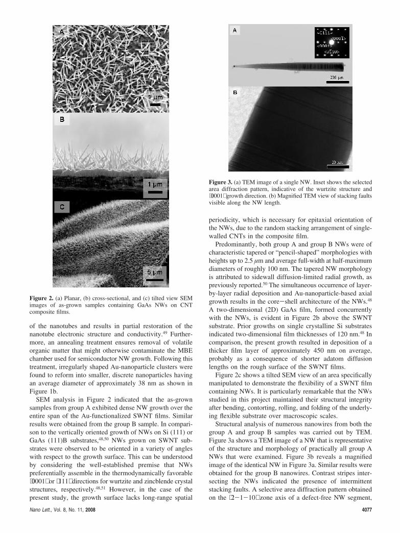
SEM analysis in Figure 2 indicated that the as-grownsamples from group A exhibited dense NW growth over theentire span of the Au-functionalized SWNT films. Similarresults were obtained from the group B sample. In compari-son to the vertically oriented growth of NWs on Si (111) orGaAs (111)B substrates,48,50 NWs grown on SWNT sub-strates were observed to be oriented in a variety of angleswith respect to the growth surface. This can be understoodby considering the well-established premise that NWspreferentially assemble in the thermodynamically favorable⟨0001⟩ or ⟨111⟩ directions for wurtzite and zincblende crystalstructures, respectively.48,51 However, in the case of thepresent study, the growth surface lacks long-range spatial
periodicity, which is necessary for epitaxial orientation ofthe NWs, due to the random stacking arrangement of single-walled CNTs in the composite film.
Predominantly, both group A and group B NWs were ofcharacteristic tapered or “pencil-shaped” morphologies withheights up to 2.5 µm and average full-width at half-maximumdiameters of roughly 100 nm. The tapered NW morphologyis attributed to sidewall diffusion-limited radial growth, aspreviously reported.50 The simultaneous occurrence of layer-by-layer radial deposition and Au-nanoparticle-based axialgrowth results in the core-shell architecture of the NWs.48
A two-dimensional (2D) GaAs film, formed concurrentlywith the NWs, is evident in Figure 2b above the SWNTsubstrate. Prior growths on single crystalline Si substratesindicated two-dimensional film thicknesses of 120 nm.48 Incomparison, the present growth resulted in deposition of athicker film layer of approximately 450 nm on average,probably as a consequence of shorter adatom diffusionlengths on the rough surface of the SWNT films.
Figure 2c shows a tilted SEM view of an area specificallymanipulated to demonstrate the flexibility of a SWNT filmcontaining NWs. It is particularly remarkable that the NWsstudied in this project maintained their structural integrityafter bending, contorting, rolling, and folding of the underly-ing flexible substrate over macroscopic scales.
Structural analysis of numerous nanowires from both thegroup A and group B samples was carried out by TEM.Figure 3a shows a TEM image of a NW that is representativeof the structure and morphology of practically all group ANWs that were examined. Figure 3b reveals a magnifiedimage of the identical NW in Figure 3a. Similar results wereobtained for the group B nanowires. Contrast stripes inter-secting the NWs indicated the presence of intermittentstacking faults. A selective area diffraction pattern obtainedon the ⟨2-1-10⟩ zone axis of a defect-free NW segment,
Figure 2. (a) Planar, (b) cross-sectional, and (c) tilted view SEMimages of as-grown samples containing GaAs NWs on CNTcomposite films.
Figure 3. (a) TEM image of a single NW. Inset shows the selectedarea diffraction pattern, indicative of the wurtzite structure and⟨0001⟩ growth direction. (b) Magnified TEM view of stacking faultsvisible along the NW length.
Nano Lett., Vol. 8, No. 11, 2008 4077
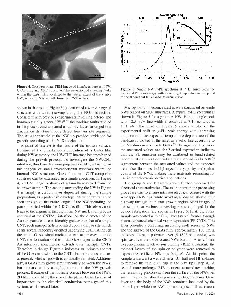
shown in the inset of Figure 3(a), confirmed a wurtzite crystalstructure with wires growing along the ⟨0001⟩ direction.Consistent with previous experiments involving hetero- andhomoepitaxially grown NWs48,52 the stacking faults studiedin the present case appeared as atomic layers arranged in azincblende structure among defect-free wurtzite segments.The Au-nanoparticle at the NW tip provides evidence forgrowth according to the VLS mechanism.
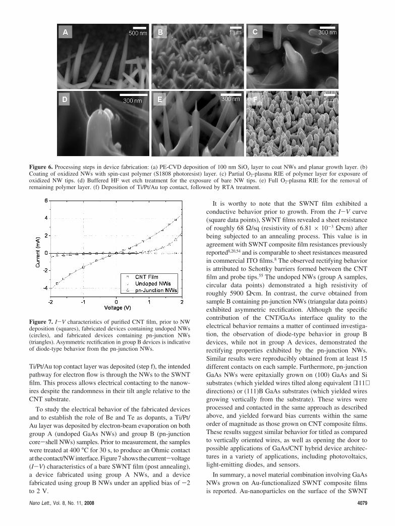
A point of interest is the nature of the growth surface.Because of the simultaneous deposition of a GaAs filmduring NW assembly, the NW/CNT interface becomes buriedduring the growth process. To investigate the NW/CNTinterface, thin lamellae were prepared via FIB, allowing forthe analysis of small cross-sectional windows where theinternal NW structure, GaAs film, and CNT-compositesubstrate can be examined in a single specimen. In Figure4, a TEM image is shown of a lamella removed from theas-grown sample. The coating surrounding the NW in Figure4 is simply a carbon layer deposited during the samplepreparation, as a protective envelope. Stacking faults can beseen throughout the entire length of the NW including theportion buried within the 2-D GaAs film. This observationleads to the argument that the initial NW nucleation processoccurred at the CNT/Au interface. As the diameter of theAu nanoparticles is considerably greater than that of a singleCNT, each nanoparticle is located upon a unique site whichspans several randomly oriented underlying CNTs. Althoughthe initial GaAs island nucleation can occur over a singleCNT, the formation of the initial GaAs layer at the CNT/Au interface, nonetheless, extends over multiple CNTs.Therefore, although Figure 4 indicates an intimate contactof the GaAs nanowires to the CNT films, it remains unclear,at present, whether growth is epitaxially initiated. Addition-ally, a GaAs film grows simultaneously between the NWs,but appears to play a negligible role in the NW growthprocess. Because of the intimate contact between the NWs,2D film, and CNTs, the role of the planar GaAs layer is ofimportance to the electrical conduction pathways of thissystem, as discussed later.
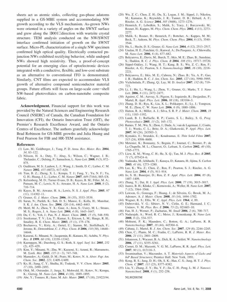
Microphotoluminescence studies were conducted on singleNWs placed on SiO2 substrates. A typical µ-PL spectrum isshown in Figure 5 for a group A NW. Here, a single peakwith 12.5 meV line width is obtained at 7 K, centered at1.51 eV. The inset of Figure 5 shows a plot of theexperimental shift in µ-PL peak energy with increasingtemperature. The expected temperature dependence of thebandgap is plotted in the inset as a solid line according tothe Varshni curve of bulk GaAs.53 The agreement betweenthe measured values and the Varshni expression indicatesthat the PL emission may be attributed to band-relatedrecombination transitions within the undoped GaAs NW.53
Agreement between the measured values and the expectedtrend also illustrates the high crystallinity, purity, and opticalquality of the NWs, making these materials promising foruse in optoelectronic device applications.
The group A and B samples were further processed forelectrical characterization. The main intent in the processingprocedure was to ensure intimate electrical contact with theAu-capped NW tips, while avoiding a possible short-circuitpathway through the planar growth region. SEM images ofthe sample, at various processing steps employed in thedevice fabrication, are shown in Figure 6. First, the entiresample was coated with a SiOx layer (step a) formed throughplasma-enhanced chemical vapor deposition (PE-CVD). Thislayer provides a conformal insulating shell across all NWsand the surface of the GaAs film, approximately 100 nm inthickness. Next, a polymer layer (S-1808 photoresist) wasspin-cast over the oxide-coated NWs (step b). After a 1 minoxygen-plasma reactive ion etching (RIE) treatment, thetopmost layers of the spin-on-polymer were removed toexpose the oxidized NW tips (step c). At this point, thesample underwent a wet etch in a 10:1 buffered HF solutionto remove the thin SiOx cap at the NW tips (step d). Asecond, more prolonged RIE treatment occurred next, etchingthe remaining photoresist from the surface of the NWs. Asseen in Figure 6e, after this processing step, the planar GaAslayer and the body of the NWs remained insulated by theoxide layer, while the NW tips are exposed. Thus, once a
Figure 4. Cross-sectional TEM image of interfaces between NW,GaAs film, and CNT substrate. The extension of stacking faultswithin the GaAs film, localized to the lateral extent of the visibleNW, indicates NW growth from the CNT surface.
Figure 5. Single NW µ-PL spectrum at 7 K. Inset plots themeasured PL peak energy with increasing temperature as comparedto the theoretical bulk GaAs Varshni curve.
4078 Nano Lett., Vol. 8, No. 11, 2008
Ti/Pt/Au top contact layer was deposited (step f), the intendedpathway for electron flow is through the NWs to the SWNTfilm. This process allows electrical contacting to the nanow-ires despite the randomness in their tilt angle relative to theCNT substrate.
To study the electrical behavior of the fabricated devicesand to establish the role of Be and Te as dopants, a Ti/Pt/Au layer was deposited by electron-beam evaporation on bothgroup A (undoped GaAs NWs) and group B (pn-junctioncore-shell NWs) samples. Prior to measurement, the sampleswere treated at 400 °C for 30 s, to produce an Ohmic contactat thecontact/NWinterface.Figure7showsthecurrent-voltage(I-V) characteristics of a bare SWNT film (post annealing),a device fabricated using group A NWs, and a devicefabricated using group B NWs under an applied bias of -2to 2 V.
It is worthy to note that the SWNT film exhibited aconductive behavior prior to growth. From the I-V curve(square data points), SWNT films revealed a sheet resistanceof roughly 68 Ω/sq (resistivity of 6.81 × 10⁻³ Ω·cm) afterbeing subjected to an annealing process. This value is inagreement with SWNT composite film resistances previouslyreported8,20,54 and is comparable to sheet resistances measuredin commercial ITO films.8 The observed rectifying behavioris attributed to Schottky barriers formed between the CNTfilm and probe tips.55 The undoped NWs (group A samples,circular data points) demonstrated a high resistivity ofroughly 5900 Ω·cm. In contrast, the curve obtained fromsample B containing pn-junction NWs (triangular data points)exhibited asymmetric rectification. Although the specificcontribution of the CNT/GaAs interface quality to theelectrical behavior remains a matter of continued investiga-tion, the observation of diode-type behavior in group Bdevices, while not in group A devices, demonstrated therectifying properties exhibited by the pn-junction NWs.Similar results were reproducibly obtained from at least 15different contacts on each sample. Furthermore, pn-junctionGaAs NWs were epitaxially grown on (100) GaAs and Sisubstrates (which yielded wires tilted along equivalent ⟨111⟩directions) or (111)B GaAs substrates (which yielded wiresgrowing vertically from the substrate). These wires wereprocessed and contacted in the same approach as describedabove, and yielded forward bias currents within the sameorder of magnitude as those grown on CNT composite films.These results suggest similar behavior for titled as comparedto vertically oriented wires, as well as opening the door topossible applications of GaAs/CNT hybrid device architec-tures in a variety of applications, including photovoltaics,light-emitting diodes, and sensors.
In summary, a novel material combination involving GaAsNWs grown on Au-functionalized SWNT composite filmsis reported. Au-nanoparticles on the surface of the SWNT
Figure 6. Processing steps in device fabrication: (a) PE-CVD deposition of 100 nm SiOx layer to coat NWs and planar growth layer. (b)Coating of oxidized NWs with spin-cast polymer (S1808 photoresist) layer. (c) Partial O2-plasma RIE of polymer layer for exposure ofoxidized NW tips. (d) Buffered HF wet etch treatment for the exposure of bare NW tips. (e) Full O2-plasma RIE for the removal ofremaining polymer layer. (f) Deposition of Ti/Pt/Au top contact, followed by RTA treatment.
Figure 7. I-V characteristics of purified CNT film, prior to NWdeposition (squares), fabricated devices containing undoped NWs(circles), and fabricated devices containing pn-junction NWs(triangles). Asymmetric rectification in group B devices is indicativeof diode-type behavior from the pn-junction NWs.
Nano Lett., Vol. 8, No. 11, 2008 4079
sheets act as atomic sinks, collecting gas-phase adatomssupplied in a GS-MBE system and accommodating NWgrowth according to the VLS mechanism. As-grown NWswere oriented in a variety of angles on the SWNT surfaceand grew along the ⟨0001⟩ direction with wurtzite crystalstructure. TEM analysis conducted on the NW/SWNTinterface confirmed initiation of growth on the SWNTsurface. Micro-PL characterization of a single NW specimenconfirmed high optical quality. Electrically contacted pn-junction NWs exhibited rectifying behavior, while undopedNWs showed high resistivity. Thus, a proof-of-conceptpotential for an emerging class of optoelectronic devicesintegrated with a conductive, flexible, and low-cost substrateas an alternative to conventional ITO is demonstrated.Similarly, CNT films are expected to accommodate VLSgrowth of alternative compound semiconductor materialgroups. Future efforts will focus on large-scale core-shellNW-based photovoltaics on carbon-nanotube compositefabric.
Acknowledgment. Financial support for this work wasprovided by the Natural Sciences and Engineering ResearchCouncil (NSERC) of Canada, the Canadian Foundation forInnovation (CFI), the Ontario Innovation Trust (OIT), thePremier’s Research Excellence Award, and the OntarioCentres of Excellence. The authors gratefully acknowledgeBrad Robinson for GS-MBE growths and Julia Huang andFred Pearson for FIB and HR-TEM assistance.
References(1) Law, M.; Goldberger, J.; Yang, P. D. Annu. ReV. Mater. Res. 2004,
34, 83–122.(2) Nilsson, H. A.; Duty, T.; Abay, S.; Wilson, C.; Wagner, J. B.;
Thelander, C.; Delsing, P.; Samuelson, L. Nano Lett. 2008, 8 (3), 872–875.
(3) Gudiksen, M. S.; Lauhon, L. J.; Wang, J.; Smith, D. C.; Lieber, C. M.Nature 2002, 415 (6872), 617–620.
(4) Tian, B. Z.; Zheng, X. L.; Kempa, T. J.; Fang, Y.; Yu, N. F.; Yu,G. H.; Huang, J. L.; Lieber, C. M. Nature 2007, 449 (7164), 885–U8.
(5) Kelzenberg, M. D.; Turner-Evans, D. B.; Kayes, B. M.; Filler, M. A.;Putnam, M. C.; Lewis, N. S.; Atwater, H. A. Nano Lett. 2008, 8 (2),710–714.
(6) Kayes, B. M.; Atwater, H. A.; Lewis, N. S. J. Appl. Phys. 2005, 97(11), 114302–11.
(7) Gruner, G. J. Mater. Chem. 2006, 16 (35), 3533–3539.(8) Saran, N.; Parikh, K.; Suh, D. S.; Munoz, E.; Kolla, H.; Manohar,
S. K. J. Am. Chem. Soc. 2004, 126 (14), 4462–4463.(9) Meitl, M. A.; Zhou, Y. X.; Gaur, A.; Jeon, S.; Usrey, M. L.; Strano,
M. S.; Rogers, J. A. Nano Lett. 2004, 4 (9), 1643–1647.(10) Du, C. S.; Yeh, J.; Pan, N. J. Mater. Chem. 2005, 15 (5), 548–550.(11) Sreekumar, T. V.; Liu, T.; Kumar, S.; Ericson, L. M.; Hauge, R. H.;
Smalley, R. E. Chem. Mater. 2003, 15 (1), 175–178.(12) Bocharova, V.; Kiriy, A.; Oertel, U.; Stamm, M.; Stoffelbach, F.;
Jerome, R.; Detrembleur, C. J. Phys. Chem. B 2006, 110 (30), 14640–14644.
(13) Kazaoui, S.; Minami, N.; Jacquemin, R.; Kataura, H.; Achiba, Y. Phys.ReV. B 1999, 60 (19), 13339–13342.
(14) Kaempgen, M.; Duesberg, G. S.; Roth, S. Appl. Surf. Sci. 2005, 252(2), 425–429.
(15) Kim, Y.; Minami, N.; Zhu, W.; Kazaoui, S.; Azumi, R.; Matsumoto,M. Synth. Met. 2003, 135 (1-3), 747–748.
(16) Mamedov, A.; Guldi, D. M.; Prato, M.; Kotov, N. A. Abstr. Pap. Am.Chem. Soc. 2002, 223, U409–U409.
(17) Ko, H.; Jiang, C. Y.; Shulha, H.; Tsukruk, V. V. Chem. Mater. 2005,17 (10), 2490–2493.
(18) Olek, M.; Ostrander, J.; Jurga, S.; Mohwald, H.; Kotov, N.; Kempa,K.; Giersig, M. Nano Lett. 2004, 4 (10), 1889–1895.
(19) Abe, Y.; Tomuro, R.; Sano, M. AdV. Mater. 2005, 17 (18), 21922194.
(20) Wu, Z. C.; Chen, Z. H.; Du, X.; Logan, J. M.; Sippel, J.; Nikolou,M.; Kamaras, K.; Reynolds, J. R.; Tanner, D. B.; Hebard, A. F.;Rinzler, A. G. Science 2004, 305 (5688), 1273–1276.
(21) Hennrich, F.; Lebedkin, S.; Malik, S.; Tracy, J.; Barczewski, M.;Rosner, H.; Kappes, M. Phys. Chem. Chem. Phys. 2002, 4 (11), 2273–2277.
(22) Malik, S.; Rosner, H.; Hennrich, F.; Bottcher, A.; Kappes, M. M.;Beck, T.; Auhorn, M. Phys. Chem. Chem. Phys. 2004, 6 (13), 3540–3544.
(23) Hu, L.; Hecht, D. S.; Gruner, G. Nano Lett. 2004, 4 (12), 2513–2517.(24) Unalan, H. E.; Fanchini, G.; Kanwal, A.; Du Pasquier, A.; Chhowalla,
M. Nano Lett. 2006, 6 (4), 677–682.(25) Bekyarova, E.; Davis, M.; Burch, T.; Itkis, M. E.; Zhao, B.; Sunshine,
S.; Haddon, R. C. J. Phys. Chem. B 2004, 108 (51), 19717–19720.(26) Sippel-Oakley, J.; Wang, H. T.; Kang, B. S.; Wu, Z. C.; Ren, F.;
Rinzler, A. G.; Pearton, S. J. Nanotechnology 2005, 16 (10), 2218–2221.
(27) Bekyarova, E.; Itkis, M. E.; Cabrera, N.; Zhao, B.; Yu, A. P.; Gao,J. B.; Haddon, R. C. J. Am. Chem. Soc. 2005, 127 (16), 5990–5995.
(28) Vichchulada, P.; Zhang, Q.; Lay, M. D. Analyst 2007, 132 (8), 719–723.
(29) Li, J.; Hu, L.; Wang, L.; Zhou, Y.; Gruner, G.; Marks, T. J. NanoLett. 2006, 6 (11), 2472–2477.
(30) Aguirre, C. M.; Auvray, S.; Pigeon, S.; Izquierdo, R.; Desjardins, P.;Martel, R. Appl. Phys. Lett. 2006, 88 (18), 183104–3.
(31) Zhang, D. H.; Ryu, K.; Liu, X. L.; Polikarpov, E.; Ly, J.; Tompson,M. E.; Zhou, C. W. Nano Lett. 2006, 6 (9), 1880–1886.
(32) Hatton, R. A.; Miller, A. J.; Silva, S. R. P. J. Mater. Chem. 2008, 18(11), 1183–1192.
(33) Landi, B. J.; Raffaelle, R. P.; Castro, S. L.; Bailey, S. G. Prog.PhotoVoltaics 2005, 13 (2), 165–172.
(34) Barnes, T. M.; Wu, X.; Zhou, J.; Duda, A.; van de Lagemaat, J.; Coutts,T. J.; Weeks, C. L.; Britz, D. A.; Glatkowski, P. Appl. Phys. Lett.2007, 90 (24), 243503–3.
(35) Kymakis, E.; Stratakis, E.; Koudoumas, E. Thin Solid Films 2007,515 (24), 8598–8600.
(36) Metenier, K.; Bonnamy, S.; Beguin, F.; Journet, C.; Bernier, P.; deLa Chapelle, M. L.; Chauvet, O.; Lefrant, S. Carbon 2002, 40 (10),1765–1773.
(37) Liew, K. M.; Wong, C. H.; He, X. Q.; Tan, M. J. Phys. ReV. B 2005,71 (7), 075424–6.
(38) Yudasaka, M.; Ichihashi, T.; Kasuya, D.; Kataura, H.; Iijima, S. Carbon2003, 41 (6), 1273–1280.
(39) Lee, K.; Wu, Z.; Chen, Z.; Ren, F.; Pearton, S. J.; Rinzler, A. G.Nano Lett. 2004, 4 (5), 911–914.
(40) Jo, S. H.; Banerjee, D.; Ren, Z. F. Appl. Phys. Lett. 2004, 85 (8),1407–1409.
(41) Zhang, Y.; Dai, H. J. Appl. Phys. Lett. 2000, 77 (19), 3015–3017.(42) Juarez, B. H.; Klinke, C.; Kornowski, A.; Weller, H. Nano Lett. 2007,
7 (12), 3564–3568.(43) Lawson, G.; Gonzaga, F.; Huang, J.; de Silveira, G.; Brook, M. A.;
Adronov, A. J. Mater. Chem. 2008, 18 (14), 1694–1702.(44) Wagner, R. S.; Ellis, W. C. Appl. Phys. Lett. 1964, 4, 89.(45) Dubrovskii, V. G.; Sibirev, N. V.; Cirlin, G. E.; Harmand, J. C.;
Ustinov, V. M. Phys. ReV. E 2006, 73 (2), 021603–10.(46) Fan, H. J.; Werner, P.; Zacharias, M. Small 2006, 2 (6), 700–717.(47) Nadarajah, A.; Word, R. C.; Meiss, J.; Konenkamp, R. Nano Lett.
2008, 8 (2), 534–537.(48) Mohseni, P. K.; Maunders, C.; Botton, G. A.; LaPierre, R. R.
Nanotechnology 2007, 18 (44), 445304–6.(49) Cabana, J.; Martel, R. J. Am. Chem. Soc. 2007, 129 (8), 2244–2245.(50) Chen, C.; Plante, M. C.; Fradin, C.; LaPierre, R. R. J. Mater. Res.
2006, 21 (11), 2801–2809.(51) Johansson, J.; Wacaser, B. A.; Dick, K. A.; Seifert, W. Nanotechnology
2006, 17 (11), S355–S361.(52) Cornet, D. M.; Mazzetti, V. G. M.; LaPierre, R. R. Appl. Phys. Lett.
2007, 90 (1), 013116–3.(53) Swaminathan, V.; Macrander, A. T. Materials Aspects of GaAs and
InP Based Structures; Prentice Hall: New York, 1991.(54) Kong, B. S.; Jung, D. H.; Oh, S. K.; Han, C. S.; Jung, H. T. J. Phys.
Chem. C 2007, 111 (23), 8377–8382.(55) Liu, Y.; Zhang, Z. Y.; Hu, Y. F.; Jin, C. H.; Peng, L. M. J. Nanosci.
Nanotechnol. 2008, 8 (1), 252–258.
NL802003M
4080 Nano Lett., Vol. 8, No. 11, 2008