NAND Flash Memory - One Laptop per Childwiki.laptop.org/images/4/48/CL1_NAND_Micron.pdf · 4Gb,...
81
Products and specifications discussed herein are subject to change by Micron without notice. 4Gb, 8Gb, and 16Gb x8 NAND Flash Memory Features PDF: 09005aef81b80e13/Source: 09005aef81b80eac Micron Technology, Inc., reserves the right to change products or specifications without notice. 4gb_nand_m40a__1.fm - Rev. B 2/07 EN 1 ©2006 Micron Technology, Inc. All rights reserved. NAND Flash Memory MT29F4G08AAA, MT29F8G08BAA, MT29F8G08DAA, MT29F16G08FAA Features • Single-level cell (SLC) technology • Organization – Page size x8: 2,112 bytes (2,048 + 64 bytes) – Block size: 64 pages (128K + 4K bytes) – Plane size: 2,048 blocks – Device size: 4Gb: 4,096 blocks; 8Gb: 8,192 blocks; 16Gb: 16,384 blocks • READ performance – Random READ: 25μs (MAX) – Sequential READ: 25ns (MIN) • WRITE performance – PROGRAM PAGE: 220μs (TYP) – BLOCK ERASE: 1.5ms (TYP) • Data retention: 10 years • Endurance: 100,000 PROGRAM/ERASE cycles • First block (block address 00h) guaranteed to be valid up to 1,000 PROGRAM/ERASE cycles 1 • Industry-standard basic NAND Flash command set • Advanced command set: – PROGRAM PAGE CACHE MODE – PAGE READ CACHE MODE – One-time programmable (OTP) commands – Two-plane commands – Interleaved die operations – READ UNIQUE ID (contact factory) – READ ID2 (contact factory) • Operation status byte provides a software method of detecting: – Operation completion – Pass/fail condition – Write-protect status • Ready/busy# (R/B#) signal provides a hardware method of detecting operation completion • WP# signal: write protect entire device • RESET required after power-up • INTERNAL DATA MOVE operations supported within the plane from which data is read Figure 1: 48-Pin TSOP Type 1 Notes: 1. For further details, see “Error Management” on page 58. 2. For part numbering and markings, see Figure 2 on page 2. 3. OCPL = off-center parting line. 4. For ET devices, contact factory. Options • Density 2 – 4Gb (single die) – 8Gb (dual-die stack 1 CE#) – 8Gb (dual-die stack 2 CE#) – 16Gb (quad-die stack) • Device width: x8 • Configuration # of die # of CE# # of R/B# I/O 1 1 1 Common 2 1 1 Common 2 2 2 Common 4 2 2 Common •VCC: 2.7–3.6V • Package – 48 TSOP type I (lead-free plating) – 48 TSOP type I OCPL 3 (lead-free plating) • Operating temperature – Commercial (0°C to +70°C) – Extended (–40°C to +85°C) 4
Transcript of NAND Flash Memory - One Laptop per Childwiki.laptop.org/images/4/48/CL1_NAND_Micron.pdf · 4Gb,...
4Gb, 8Gb, and 16Gb x8 NAND Flash MemoryFeatures
NAND Flash MemoryMT29F4G08AAA, MT29F8G08BAA, MT29F8G08DAA, MT29F16G08FAA
Features• Single-level cell (SLC) technology• Organization
– Page size x8: 2,112 bytes (2,048 + 64 bytes)– Block size: 64 pages (128K + 4K bytes)– Plane size: 2,048 blocks– Device size: 4Gb: 4,096 blocks; 8Gb: 8,192 blocks;
16Gb: 16,384 blocks• READ performance
– Random READ: 25µs (MAX)– Sequential READ: 25ns (MIN)
• WRITE performance– PROGRAM PAGE: 220µs (TYP)– BLOCK ERASE: 1.5ms (TYP)
• Data retention: 10 years• Endurance: 100,000 PROGRAM/ERASE cycles• First block (block address 00h) guaranteed to be
valid up to 1,000 PROGRAM/ERASE cycles1
• Industry-standard basic NAND Flash command set• Advanced command set:
– PROGRAM PAGE CACHE MODE– PAGE READ CACHE MODE– One-time programmable (OTP) commands– Two-plane commands– Interleaved die operations– READ UNIQUE ID (contact factory)– READ ID2 (contact factory)
• Operation status byte provides a software method of detecting:– Operation completion– Pass/fail condition– Write-protect status
• Ready/busy# (R/B#) signal provides a hardware method of detecting operation completion
• WP# signal: write protect entire device• RESET required after power-up• INTERNAL DATA MOVE operations supported
within the plane from which data is read
Products and specifications discussed herein are
PDF: 09005aef81b80e13/Source: 09005aef81b80eac4gb_nand_m40a__1.fm - Rev. B 2/07 EN 1
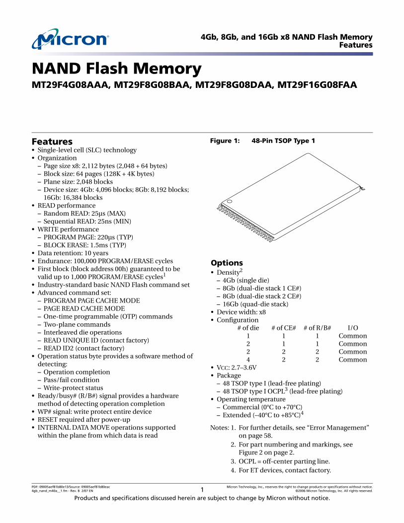
Figure 1: 48-Pin TSOP Type 1
Notes: 1. For further details, see “Error Management” on page 58.
2. For part numbering and markings, see Figure 2 on page 2.
3. OCPL = off-center parting line.4. For ET devices, contact factory.
Options • Density2
– 4Gb (single die)– 8Gb (dual-die stack 1 CE#)– 8Gb (dual-die stack 2 CE#)– 16Gb (quad-die stack)
• Device width: x8• Configuration
# of die # of CE# # of R/B# I/O1 1 1 Common2 1 1 Common2 2 2 Common4 2 2 Common
• VCC: 2.7–3.6V• Package
– 48 TSOP type I (lead-free plating)– 48 TSOP type I OCPL3 (lead-free plating)
• Operating temperature – Commercial (0°C to +70°C)– Extended (–40°C to +85°C)4
subject to change by Micron without notice.
Micron Technology, Inc., reserves the right to change products or specifications without notice.©2006 Micron Technology, Inc. All rights reserved.
4Gb, 8Gb, and 16Gb x8 NAND Flash MemoryPart Numbering Information
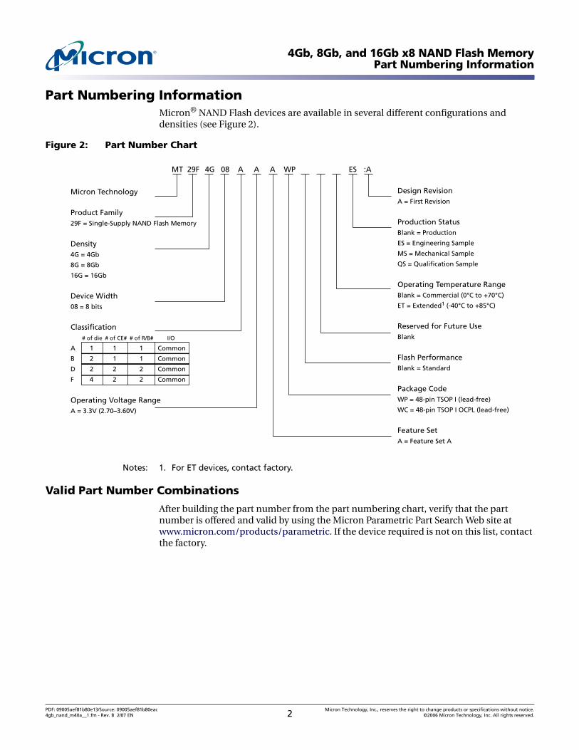
Part Numbering InformationMicron® NAND Flash devices are available in several different configurations and densities (see Figure 2).
Figure 2: Part Number Chart
Notes: 1. For ET devices, contact factory.
Valid Part Number Combinations
After building the part number from the part numbering chart, verify that the part number is offered and valid by using the Micron Parametric Part Search Web site at www.micron.com/products/parametric. If the device required is not on this list, contact the factory.
MT 29F 4G 08 A A A WP ES :A
Micron Technology
Product Family29F = Single-Supply NAND Flash Memory
Density4G = 4Gb
8G = 8Gb
16G = 16Gb
Device Width08 = 8 bits
Operating Voltage RangeA = 3.3V (2.70–3.60V)
Design RevisionA = First Revision
Production StatusBlank = Production
ES = Engineering Sample
MS = Mechanical Sample
QS = Qualification Sample
Operating Temperature RangeBlank = Commercial (0°C to +70°C)
ET = Extended1 (-40°C to +85°C)
Reserved for Future UseBlank
Flash PerformanceBlank = Standard
Package CodeWP = 48-pin TSOP I (lead-free)
WC = 48-pin TSOP I OCPL (lead-free)
Feature SetA = Feature Set A
Classification# of die # of CE# # of R/B# I/O
A 1 1 1 Common
B 2 1 1 Common
D 2 2 2 Common
F 4 2 2 Common
PDF: 09005aef81b80e13/Source: 09005aef81b80eac Micron Technology, Inc., reserves the right to change products or specifications without notice.4gb_nand_m40a__1.fm - Rev. B 2/07 EN 2 ©2006 Micron Technology, Inc. All rights reserved.
4Gb, 8Gb, and 16Gb x8 NAND Flash MemoryTable of Contents
Table of ContentsFeatures . . . . . . . . . . . . . . . . . . . . . . . . . . . . . . . . . . . . . . . . . . . . . . . . . . . . . . . . . . . . . . . . . . . . . . . . . . . . . . . . . . . . . . . . . . . . . .1Part Numbering Information . . . . . . . . . . . . . . . . . . . . . . . . . . . . . . . . . . . . . . . . . . . . . . . . . . . . . . . . . . . . . . . . . . . . . . . . . . .2
Valid Part Number Combinations . . . . . . . . . . . . . . . . . . . . . . . . . . . . . . . . . . . . . . . . . . . . . . . . . . . . . . . . . . . . . . . . . . . .2General Description . . . . . . . . . . . . . . . . . . . . . . . . . . . . . . . . . . . . . . . . . . . . . . . . . . . . . . . . . . . . . . . . . . . . . . . . . . . . . . . . . . .8Architecture . . . . . . . . . . . . . . . . . . . . . . . . . . . . . . . . . . . . . . . . . . . . . . . . . . . . . . . . . . . . . . . . . . . . . . . . . . . . . . . . . . . . . . . . .11Addressing . . . . . . . . . . . . . . . . . . . . . . . . . . . . . . . . . . . . . . . . . . . . . . . . . . . . . . . . . . . . . . . . . . . . . . . . . . . . . . . . . . . . . . . . . .12Memory Mapping . . . . . . . . . . . . . . . . . . . . . . . . . . . . . . . . . . . . . . . . . . . . . . . . . . . . . . . . . . . . . . . . . . . . . . . . . . . . . . . . . . . .12Array Organization . . . . . . . . . . . . . . . . . . . . . . . . . . . . . . . . . . . . . . . . . . . . . . . . . . . . . . . . . . . . . . . . . . . . . . . . . . . . . . . . . . .13Bus Operation . . . . . . . . . . . . . . . . . . . . . . . . . . . . . . . . . . . . . . . . . . . . . . . . . . . . . . . . . . . . . . . . . . . . . . . . . . . . . . . . . . . . . . .15
Control Signals . . . . . . . . . . . . . . . . . . . . . . . . . . . . . . . . . . . . . . . . . . . . . . . . . . . . . . . . . . . . . . . . . . . . . . . . . . . . . . . . . . . .15Commands . . . . . . . . . . . . . . . . . . . . . . . . . . . . . . . . . . . . . . . . . . . . . . . . . . . . . . . . . . . . . . . . . . . . . . . . . . . . . . . . . . . . . . .15Address Input . . . . . . . . . . . . . . . . . . . . . . . . . . . . . . . . . . . . . . . . . . . . . . . . . . . . . . . . . . . . . . . . . . . . . . . . . . . . . . . . . . . . .15Data Input . . . . . . . . . . . . . . . . . . . . . . . . . . . . . . . . . . . . . . . . . . . . . . . . . . . . . . . . . . . . . . . . . . . . . . . . . . . . . . . . . . . . . . . .16READs . . . . . . . . . . . . . . . . . . . . . . . . . . . . . . . . . . . . . . . . . . . . . . . . . . . . . . . . . . . . . . . . . . . . . . . . . . . . . . . . . . . . . . . . . . . .16Ready/Busy# . . . . . . . . . . . . . . . . . . . . . . . . . . . . . . . . . . . . . . . . . . . . . . . . . . . . . . . . . . . . . . . . . . . . . . . . . . . . . . . . . . . . . .16
Command Definitions . . . . . . . . . . . . . . . . . . . . . . . . . . . . . . . . . . . . . . . . . . . . . . . . . . . . . . . . . . . . . . . . . . . . . . . . . . . . . . . .19READ Operations . . . . . . . . . . . . . . . . . . . . . . . . . . . . . . . . . . . . . . . . . . . . . . . . . . . . . . . . . . . . . . . . . . . . . . . . . . . . . . . . . .21
PAGE READ 00h-30h. . . . . . . . . . . . . . . . . . . . . . . . . . . . . . . . . . . . . . . . . . . . . . . . . . . . . . . . . . . . . . . . . . . . . . . . . . . . .21RANDOM DATA READ 05h-E0h. . . . . . . . . . . . . . . . . . . . . . . . . . . . . . . . . . . . . . . . . . . . . . . . . . . . . . . . . . . . . . . . . . .22PAGE READ CACHE MODE START 31h; PAGE READ CACHE MODE START LAST 3Fh. . . . . . . . . . . . . . . . . .22READ ID 90h . . . . . . . . . . . . . . . . . . . . . . . . . . . . . . . . . . . . . . . . . . . . . . . . . . . . . . . . . . . . . . . . . . . . . . . . . . . . . . . . . . . .24READ STATUS 70h . . . . . . . . . . . . . . . . . . . . . . . . . . . . . . . . . . . . . . . . . . . . . . . . . . . . . . . . . . . . . . . . . . . . . . . . . . . . . .26
PROGRAM Operations . . . . . . . . . . . . . . . . . . . . . . . . . . . . . . . . . . . . . . . . . . . . . . . . . . . . . . . . . . . . . . . . . . . . . . . . . . . . .27PROGRAM PAGE 80h-10h . . . . . . . . . . . . . . . . . . . . . . . . . . . . . . . . . . . . . . . . . . . . . . . . . . . . . . . . . . . . . . . . . . . . . . . .27SERIAL DATA INPUT 80h . . . . . . . . . . . . . . . . . . . . . . . . . . . . . . . . . . . . . . . . . . . . . . . . . . . . . . . . . . . . . . . . . . . . . . . .27RANDOM DATA INPUT 85h . . . . . . . . . . . . . . . . . . . . . . . . . . . . . . . . . . . . . . . . . . . . . . . . . . . . . . . . . . . . . . . . . . . . . .27PROGRAM PAGE CACHE MODE 80h-15h. . . . . . . . . . . . . . . . . . . . . . . . . . . . . . . . . . . . . . . . . . . . . . . . . . . . . . . . . .28
Internal Data Move . . . . . . . . . . . . . . . . . . . . . . . . . . . . . . . . . . . . . . . . . . . . . . . . . . . . . . . . . . . . . . . . . . . . . . . . . . . . . . . .29READ FOR INTERNAL DATA MOVE 00h-35h . . . . . . . . . . . . . . . . . . . . . . . . . . . . . . . . . . . . . . . . . . . . . . . . . . . . . . .29PROGRAM for INTERNAL DATA MOVE 85h-10h. . . . . . . . . . . . . . . . . . . . . . . . . . . . . . . . . . . . . . . . . . . . . . . . . . . .29
BLOCK ERASE Operation . . . . . . . . . . . . . . . . . . . . . . . . . . . . . . . . . . . . . . . . . . . . . . . . . . . . . . . . . . . . . . . . . . . . . . . . . . .30BLOCK ERASE 60h-D0h . . . . . . . . . . . . . . . . . . . . . . . . . . . . . . . . . . . . . . . . . . . . . . . . . . . . . . . . . . . . . . . . . . . . . . . . . .30
One-Time Programmable (OTP) Area . . . . . . . . . . . . . . . . . . . . . . . . . . . . . . . . . . . . . . . . . . . . . . . . . . . . . . . . . . . . . . . .31OTP DATA PROGRAM A0h-10h . . . . . . . . . . . . . . . . . . . . . . . . . . . . . . . . . . . . . . . . . . . . . . . . . . . . . . . . . . . . . . . . . . .32OTP DATA PROTECT A5h-10h . . . . . . . . . . . . . . . . . . . . . . . . . . . . . . . . . . . . . . . . . . . . . . . . . . . . . . . . . . . . . . . . . . . .34OTP DATA READ AFh-30h. . . . . . . . . . . . . . . . . . . . . . . . . . . . . . . . . . . . . . . . . . . . . . . . . . . . . . . . . . . . . . . . . . . . . . . .34
TWO-PLANE Operations . . . . . . . . . . . . . . . . . . . . . . . . . . . . . . . . . . . . . . . . . . . . . . . . . . . . . . . . . . . . . . . . . . . . . . . . . . .35Two-Plane Addressing . . . . . . . . . . . . . . . . . . . . . . . . . . . . . . . . . . . . . . . . . . . . . . . . . . . . . . . . . . . . . . . . . . . . . . . . . . .35TWO-PLANE PAGE READ 00h-00h-30h . . . . . . . . . . . . . . . . . . . . . . . . . . . . . . . . . . . . . . . . . . . . . . . . . . . . . . . . . . . .36TWO-PLANE RANDOM DATA READ 06h-E0h . . . . . . . . . . . . . . . . . . . . . . . . . . . . . . . . . . . . . . . . . . . . . . . . . . . . . .36TWO-PLANE PROGRAM PAGE 80h-11h-80h-10h . . . . . . . . . . . . . . . . . . . . . . . . . . . . . . . . . . . . . . . . . . . . . . . . . . .39TWO-PLANE PROGRAM PAGE CACHE MODE 80h-11h-80h-15h . . . . . . . . . . . . . . . . . . . . . . . . . . . . . . . . . . . . .40TWO-PLANE INTERNAL DATA MOVE 00h-00h-35h/85h-11h-80h-10h. . . . . . . . . . . . . . . . . . . . . . . . . . . . . . . .42TWO-PLANE READ for INTERNAL DATA MOVE 00h-00h-35h . . . . . . . . . . . . . . . . . . . . . . . . . . . . . . . . . . . . . . .42TWO-PLANE PROGRAM for INTERNAL DATA MOVE 85h-11h-80h-10h. . . . . . . . . . . . . . . . . . . . . . . . . . . . . . .43TWO-PLANE BLOCK ERASE 60h-60h-D0h . . . . . . . . . . . . . . . . . . . . . . . . . . . . . . . . . . . . . . . . . . . . . . . . . . . . . . . . .45TWO-PLANE/MULTIPLE-DIE READ STATUS 78h . . . . . . . . . . . . . . . . . . . . . . . . . . . . . . . . . . . . . . . . . . . . . . . . . .46
Interleaved Die Operations . . . . . . . . . . . . . . . . . . . . . . . . . . . . . . . . . . . . . . . . . . . . . . . . . . . . . . . . . . . . . . . . . . . . . . . . .47Interleaved PROGRAM PAGE Operations . . . . . . . . . . . . . . . . . . . . . . . . . . . . . . . . . . . . . . . . . . . . . . . . . . . . . . . . . .47Interleaved PROGRAM PAGE CACHE MODE Operations . . . . . . . . . . . . . . . . . . . . . . . . . . . . . . . . . . . . . . . . . . . .48Interleaved TWO-PLANE PROGRAM PAGE Operations. . . . . . . . . . . . . . . . . . . . . . . . . . . . . . . . . . . . . . . . . . . . . .49Interleaved TWO-PLANE PROGRAM PAGE CACHE MODE Operations. . . . . . . . . . . . . . . . . . . . . . . . . . . . . . . .52Interleaved BLOCK ERASE Operations. . . . . . . . . . . . . . . . . . . . . . . . . . . . . . . . . . . . . . . . . . . . . . . . . . . . . . . . . . . . .54Interleaved TWO-PLANE BLOCK ERASE Operations . . . . . . . . . . . . . . . . . . . . . . . . . . . . . . . . . . . . . . . . . . . . . . . .54
RESET Operation . . . . . . . . . . . . . . . . . . . . . . . . . . . . . . . . . . . . . . . . . . . . . . . . . . . . . . . . . . . . . . . . . . . . . . . . . . . . . . . . . .56RESET FFh. . . . . . . . . . . . . . . . . . . . . . . . . . . . . . . . . . . . . . . . . . . . . . . . . . . . . . . . . . . . . . . . . . . . . . . . . . . . . . . . . . . . . .56
PDF: 09005aef81b80e13/Source: 09005aef81b80eac Micron Technology, Inc., reserves the right to change products or specifications without notice.4gb_nand_m40aTOC.fm - Rev. B 2/07 EN 3 ©2006 Micron Technology, Inc. All rights reserved.
4Gb, 8Gb, and 16Gb x8 NAND Flash MemoryTable of Contents
WRITE PROTECT Operation . . . . . . . . . . . . . . . . . . . . . . . . . . . . . . . . . . . . . . . . . . . . . . . . . . . . . . . . . . . . . . . . . . . . . . . .57Error Management . . . . . . . . . . . . . . . . . . . . . . . . . . . . . . . . . . . . . . . . . . . . . . . . . . . . . . . . . . . . . . . . . . . . . . . . . . . . . . . . . . .58Electrical Characteristics . . . . . . . . . . . . . . . . . . . . . . . . . . . . . . . . . . . . . . . . . . . . . . . . . . . . . . . . . . . . . . . . . . . . . . . . . . . . . .59
VCC Power Cycling . . . . . . . . . . . . . . . . . . . . . . . . . . . . . . . . . . . . . . . . . . . . . . . . . . . . . . . . . . . . . . . . . . . . . . . . . . . . . . . . .60Timing Diagrams. . . . . . . . . . . . . . . . . . . . . . . . . . . . . . . . . . . . . . . . . . . . . . . . . . . . . . . . . . . . . . . . . . . . . . . . . . . . . . . . . . . . .65Package Dimensions . . . . . . . . . . . . . . . . . . . . . . . . . . . . . . . . . . . . . . . . . . . . . . . . . . . . . . . . . . . . . . . . . . . . . . . . . . . . . . . . .79
PDF: 09005aef81b80e13/Source: 09005aef81b80eac Micron Technology, Inc., reserves the right to change products or specifications without notice.4gb_nand_m40aTOC.fm - Rev. B 2/07 EN 4 ©2006 Micron Technology, Inc. All rights reserved.
4Gb, 8Gb, and 16Gb x8 NAND Flash MemoryList of Figures
List of FiguresFigure 1: 48-Pin TSOP Type 1 . . . . . . . . . . . . . . . . . . . . . . . . . . . . . . . . . . . . . . . . . . . . . . . . . . . . . . . . . . . . . . . . . . . . . . .1Figure 2: Part Number Chart . . . . . . . . . . . . . . . . . . . . . . . . . . . . . . . . . . . . . . . . . . . . . . . . . . . . . . . . . . . . . . . . . . . . . . . .2Figure 3: 48-Pin TSOP Type 1 Pin Assignment (Top View) . . . . . . . . . . . . . . . . . . . . . . . . . . . . . . . . . . . . . . . . . . . . . .9Figure 4: NAND Flash Functional Block Diagram . . . . . . . . . . . . . . . . . . . . . . . . . . . . . . . . . . . . . . . . . . . . . . . . . . . .11Figure 5: Memory Map . . . . . . . . . . . . . . . . . . . . . . . . . . . . . . . . . . . . . . . . . . . . . . . . . . . . . . . . . . . . . . . . . . . . . . . . . . . .12Figure 6: Array Organization for MT29F4G08AAA and MT29F8G08DAA (x8) . . . . . . . . . . . . . . . . . . . . . . . . . . . .13Figure 7: Array Organization for MT29F8G08BAA and MT29F16G08FAA (x8). . . . . . . . . . . . . . . . . . . . . . . . . . . .14Figure 8: READY/BUSY# Open Drain . . . . . . . . . . . . . . . . . . . . . . . . . . . . . . . . . . . . . . . . . . . . . . . . . . . . . . . . . . . . . . .17Figure 9: tFall and tRise . . . . . . . . . . . . . . . . . . . . . . . . . . . . . . . . . . . . . . . . . . . . . . . . . . . . . . . . . . . . . . . . . . . . . . . . . . .17Figure 10: Iol vs. Rp . . . . . . . . . . . . . . . . . . . . . . . . . . . . . . . . . . . . . . . . . . . . . . . . . . . . . . . . . . . . . . . . . . . . . . . . . . . . . . . .18Figure 11: TC vs. Rp . . . . . . . . . . . . . . . . . . . . . . . . . . . . . . . . . . . . . . . . . . . . . . . . . . . . . . . . . . . . . . . . . . . . . . . . . . . . . . . .18Figure 12: PAGE READ Operation . . . . . . . . . . . . . . . . . . . . . . . . . . . . . . . . . . . . . . . . . . . . . . . . . . . . . . . . . . . . . . . . . . .21Figure 13: RANDOM DATA READ Operation . . . . . . . . . . . . . . . . . . . . . . . . . . . . . . . . . . . . . . . . . . . . . . . . . . . . . . . . .22Figure 14: PAGE READ CACHE MODE Operation . . . . . . . . . . . . . . . . . . . . . . . . . . . . . . . . . . . . . . . . . . . . . . . . . . . . .23Figure 15: READ ID Operation . . . . . . . . . . . . . . . . . . . . . . . . . . . . . . . . . . . . . . . . . . . . . . . . . . . . . . . . . . . . . . . . . . . . . .24Figure 16: Status Register Operation . . . . . . . . . . . . . . . . . . . . . . . . . . . . . . . . . . . . . . . . . . . . . . . . . . . . . . . . . . . . . . . . .27Figure 17: PROGRAM and READ STATUS Operation . . . . . . . . . . . . . . . . . . . . . . . . . . . . . . . . . . . . . . . . . . . . . . . . . .28Figure 18: RANDOM DATA INPUT Operation . . . . . . . . . . . . . . . . . . . . . . . . . . . . . . . . . . . . . . . . . . . . . . . . . . . . . . . .28Figure 19: PROGRAM PAGE CACHE MODE Operation Example . . . . . . . . . . . . . . . . . . . . . . . . . . . . . . . . . . . . . . . .29Figure 20: INTERNAL DATA MOVE Operation . . . . . . . . . . . . . . . . . . . . . . . . . . . . . . . . . . . . . . . . . . . . . . . . . . . . . . . .30Figure 21: INTERNAL DATA MOVE Operation with RANDOM DATA INPUT . . . . . . . . . . . . . . . . . . . . . . . . . . . . .30Figure 22: BLOCK ERASE Operation . . . . . . . . . . . . . . . . . . . . . . . . . . . . . . . . . . . . . . . . . . . . . . . . . . . . . . . . . . . . . . . . .31Figure 23: OTP DATA PROGRAM Operation . . . . . . . . . . . . . . . . . . . . . . . . . . . . . . . . . . . . . . . . . . . . . . . . . . . . . . . . . .33Figure 24: OTP DATA PROTECT Operation . . . . . . . . . . . . . . . . . . . . . . . . . . . . . . . . . . . . . . . . . . . . . . . . . . . . . . . . . . .34Figure 25: OTP DATA READ Operation. . . . . . . . . . . . . . . . . . . . . . . . . . . . . . . . . . . . . . . . . . . . . . . . . . . . . . . . . . . . . . .35Figure 26: TWO-PLANE PAGE READ Operation . . . . . . . . . . . . . . . . . . . . . . . . . . . . . . . . . . . . . . . . . . . . . . . . . . . . . . .37Figure 27: TWO-PLANE PAGE READ Operation with RANDOM DATA READ . . . . . . . . . . . . . . . . . . . . . . . . . . . . .38Figure 28: TWO-PLANE PROGRAM PAGE Operation . . . . . . . . . . . . . . . . . . . . . . . . . . . . . . . . . . . . . . . . . . . . . . . . . .39Figure 29: TWO-PLANE PROGRAM PAGE Operation with RANDOM DATA INPUT . . . . . . . . . . . . . . . . . . . . . . .40Figure 30: TWO-PLANE PROGRAM PAGE CACHE MODE Operation . . . . . . . . . . . . . . . . . . . . . . . . . . . . . . . . . . . .42Figure 31: TWO-PLANE INTERNAL DATA MOVE Operation . . . . . . . . . . . . . . . . . . . . . . . . . . . . . . . . . . . . . . . . . . .44Figure 32: TWO-PLANE INTERNAL DATA MOVE Operation with RANDOM DATA INPUT . . . . . . . . . . . . . . . .44Figure 33: TWO-PLANE BLOCK ERASE Operation. . . . . . . . . . . . . . . . . . . . . . . . . . . . . . . . . . . . . . . . . . . . . . . . . . . . .45Figure 34: TWO-PLANE/MULTIPLE-DIE READ STATUS Cycle . . . . . . . . . . . . . . . . . . . . . . . . . . . . . . . . . . . . . . . . .46Figure 35: Interleaved PROGRAM PAGE Operation with R/B# Monitoring . . . . . . . . . . . . . . . . . . . . . . . . . . . . . . .47Figure 36: Interleaved PROGRAM PAGE Operation with Status Register Monitoring . . . . . . . . . . . . . . . . . . . . . .48Figure 37: Interleaved PROGRAM PAGE CACHE MODE Operation with R/B# Monitoring . . . . . . . . . . . . . . . . .48Figure 38: Interleaved PROGRAM PAGE CACHE MODE Operation with Status Register Monitoring . . . . . . . .49Figure 39: Interleaved TWO-PLANE PROGRAM PAGE Operation with R/B# Monitoring. . . . . . . . . . . . . . . . . . .50Figure 40: Interleaved TWO-PLANE PROGRAM PAGE Operation with Status Register Monitoring. . . . . . . . . .51Figure 41: Interleaved TWO-PLANE PROGRAM PAGE CACHE MODE Operation with R/B# Monitoring . . . .52Figure 42: Interleaved TWO-PLANE PROGRAM PAGE CACHE MODE Operation with Status Register
Monitoring . . . . . . . . . . . . . . . . . . . . . . . . . . . . . . . . . . . . . . . . . . . . . . . . . . . . . . . . . . . . . . . . . . . . . . . . . . . . . .53Figure 43: Interleaved BLOCK ERASE Operation with R/B# Monitoring . . . . . . . . . . . . . . . . . . . . . . . . . . . . . . . . .54Figure 44: Interleaved BLOCK ERASE Operation with Status Register Monitoring. . . . . . . . . . . . . . . . . . . . . . . . .54Figure 45: Interleaved TWO-PLANE BLOCK ERASE Operation with R/B# Monitoring . . . . . . . . . . . . . . . . . . . . .55Figure 46: Interleaved TWO-PLANE BLOCK ERASE Operation with Status Register Monitoring . . . . . . . . . . . .55Figure 47: RESET Operation . . . . . . . . . . . . . . . . . . . . . . . . . . . . . . . . . . . . . . . . . . . . . . . . . . . . . . . . . . . . . . . . . . . . . . . .56Figure 48: ERASE Enable . . . . . . . . . . . . . . . . . . . . . . . . . . . . . . . . . . . . . . . . . . . . . . . . . . . . . . . . . . . . . . . . . . . . . . . . . . .57Figure 49: ERASE Disable . . . . . . . . . . . . . . . . . . . . . . . . . . . . . . . . . . . . . . . . . . . . . . . . . . . . . . . . . . . . . . . . . . . . . . . . . . .57Figure 50: PROGRAM Enable . . . . . . . . . . . . . . . . . . . . . . . . . . . . . . . . . . . . . . . . . . . . . . . . . . . . . . . . . . . . . . . . . . . . . . .57Figure 51: PROGRAM Disable . . . . . . . . . . . . . . . . . . . . . . . . . . . . . . . . . . . . . . . . . . . . . . . . . . . . . . . . . . . . . . . . . . . . . . .58Figure 52: AC Waveforms During Power Transitions. . . . . . . . . . . . . . . . . . . . . . . . . . . . . . . . . . . . . . . . . . . . . . . . . . .60Figure 53: COMMAND LATCH Cycle . . . . . . . . . . . . . . . . . . . . . . . . . . . . . . . . . . . . . . . . . . . . . . . . . . . . . . . . . . . . . . . .65Figure 54: ADDRESS LATCH Cycle . . . . . . . . . . . . . . . . . . . . . . . . . . . . . . . . . . . . . . . . . . . . . . . . . . . . . . . . . . . . . . . . . .65Figure 55: INPUT DATA LATCH Cycle . . . . . . . . . . . . . . . . . . . . . . . . . . . . . . . . . . . . . . . . . . . . . . . . . . . . . . . . . . . . . . .66
PDF: 09005aef81b80e13/Source: 09005aef81b80eac Micron Technology, Inc., reserves the right to change products or specifications without notice.4gb_nand_m40aLOF.fm - Rev. B 2/07 EN 5 ©2006 Micron Technology, Inc. All rights reserved.
4Gb, 8Gb, and 16Gb x8 NAND Flash MemoryList of Figures
Figure 56: SERIAL ACCESS Cycle After READ . . . . . . . . . . . . . . . . . . . . . . . . . . . . . . . . . . . . . . . . . . . . . . . . . . . . . . . . .66Figure 57: SERIAL ACCESS Cycle After READ (EDO Mode) . . . . . . . . . . . . . . . . . . . . . . . . . . . . . . . . . . . . . . . . . . . . .67Figure 58: READ STATUS Operation . . . . . . . . . . . . . . . . . . . . . . . . . . . . . . . . . . . . . . . . . . . . . . . . . . . . . . . . . . . . . . . . .67Figure 59: TWO-PLANE/MULTIPLE-DIE READ STATUS Operation . . . . . . . . . . . . . . . . . . . . . . . . . . . . . . . . . . . . .68Figure 60: PAGE READ Operation . . . . . . . . . . . . . . . . . . . . . . . . . . . . . . . . . . . . . . . . . . . . . . . . . . . . . . . . . . . . . . . . . . .68Figure 61: READ Operation with CE# “Don’t Care” . . . . . . . . . . . . . . . . . . . . . . . . . . . . . . . . . . . . . . . . . . . . . . . . . . . .69Figure 62: RANDOM DATA READ Operation . . . . . . . . . . . . . . . . . . . . . . . . . . . . . . . . . . . . . . . . . . . . . . . . . . . . . . . . .69Figure 63: PAGE READ CACHE MODE Operation, Part 1 of 2 . . . . . . . . . . . . . . . . . . . . . . . . . . . . . . . . . . . . . . . . . . .70Figure 64: PAGE READ CACHE MODE Operation, Part 2 of 2 . . . . . . . . . . . . . . . . . . . . . . . . . . . . . . . . . . . . . . . . . . .71Figure 65: PAGE READ CACHE MODE Operation without R/B#, Part 1 of 2 . . . . . . . . . . . . . . . . . . . . . . . . . . . . . .72Figure 66: PAGE READ CACHE MODE Operation without R/B#, Part 2 of 2 . . . . . . . . . . . . . . . . . . . . . . . . . . . . . .73Figure 67: READ ID Operation . . . . . . . . . . . . . . . . . . . . . . . . . . . . . . . . . . . . . . . . . . . . . . . . . . . . . . . . . . . . . . . . . . . . . .74Figure 68: PROGRAM PAGE Operation. . . . . . . . . . . . . . . . . . . . . . . . . . . . . . . . . . . . . . . . . . . . . . . . . . . . . . . . . . . . . . .74Figure 69: Program Operation with CE# “Don’t Care” . . . . . . . . . . . . . . . . . . . . . . . . . . . . . . . . . . . . . . . . . . . . . . . . .75Figure 70: PROGRAM PAGE Operation with RANDOM DATA INPUT. . . . . . . . . . . . . . . . . . . . . . . . . . . . . . . . . . . .75Figure 71: INTERNAL DATA MOVE Operation . . . . . . . . . . . . . . . . . . . . . . . . . . . . . . . . . . . . . . . . . . . . . . . . . . . . . . . .76Figure 72: PROGRAM PAGE CACHE MODE Operation. . . . . . . . . . . . . . . . . . . . . . . . . . . . . . . . . . . . . . . . . . . . . . . . .76Figure 73: PROGRAM PAGE CACHE MODE Operation Ending on 15h. . . . . . . . . . . . . . . . . . . . . . . . . . . . . . . . . . .77Figure 74: BLOCK ERASE Operation . . . . . . . . . . . . . . . . . . . . . . . . . . . . . . . . . . . . . . . . . . . . . . . . . . . . . . . . . . . . . . . . .78Figure 75: RESET Operation . . . . . . . . . . . . . . . . . . . . . . . . . . . . . . . . . . . . . . . . . . . . . . . . . . . . . . . . . . . . . . . . . . . . . . . .78Figure 76: 48-Pin TSOP Type 1 (WP Package Code) . . . . . . . . . . . . . . . . . . . . . . . . . . . . . . . . . . . . . . . . . . . . . . . . . . . .79Figure 77: 48-Pin TSOP OCPL Type 1 (WC Package Code) . . . . . . . . . . . . . . . . . . . . . . . . . . . . . . . . . . . . . . . . . . . . . .80
PDF: 09005aef81b80e13/Source: 09005aef81b80eac Micron Technology, Inc., reserves the right to change products or specifications without notice.4gb_nand_m40aLOF.fm - Rev. B 2/07 EN 6 ©2006 Micron Technology, Inc. All rights reserved.
PDF: 09005aef81b80e13/Source: 09005aef81b80eac Micron Technology, Inc., reserves the right to change products or specifications without notice.4gb_nand_m40aLOT.fm - Rev. B 2/07 EN 7 ©2006 Micron Technology, Inc. All rights reserved.
4Gb, 8Gb, and 16Gb x8 NAND Flash MemoryList of Tables
List of TablesTable 1: Signal Descriptions. . . . . . . . . . . . . . . . . . . . . . . . . . . . . . . . . . . . . . . . . . . . . . . . . . . . . . . . . . . . . . . . . . . . . . .10Table 2: Operational Example . . . . . . . . . . . . . . . . . . . . . . . . . . . . . . . . . . . . . . . . . . . . . . . . . . . . . . . . . . . . . . . . . . . . .12Table 3: Array Addressing: MT29F4G08AAA and MT29F8G08DAA. . . . . . . . . . . . . . . . . . . . . . . . . . . . . . . . . . . . .13Table 4: Array Addressing: MT28F8G08BAA and MT29F16G08FAA . . . . . . . . . . . . . . . . . . . . . . . . . . . . . . . . . . . .14Table 5: Mode Selection . . . . . . . . . . . . . . . . . . . . . . . . . . . . . . . . . . . . . . . . . . . . . . . . . . . . . . . . . . . . . . . . . . . . . . . . . .18Table 6: Command Set . . . . . . . . . . . . . . . . . . . . . . . . . . . . . . . . . . . . . . . . . . . . . . . . . . . . . . . . . . . . . . . . . . . . . . . . . . .19Table 7: Two-Plane Command Set . . . . . . . . . . . . . . . . . . . . . . . . . . . . . . . . . . . . . . . . . . . . . . . . . . . . . . . . . . . . . . . . .20Table 8: Device ID and Configuration Codes. . . . . . . . . . . . . . . . . . . . . . . . . . . . . . . . . . . . . . . . . . . . . . . . . . . . . . . .25Table 9: Status Register Bit Definition . . . . . . . . . . . . . . . . . . . . . . . . . . . . . . . . . . . . . . . . . . . . . . . . . . . . . . . . . . . . . .26Table 10: Status Register Contents After RESET Operation . . . . . . . . . . . . . . . . . . . . . . . . . . . . . . . . . . . . . . . . . . . .56Table 11: Absolute Maximum Ratings . . . . . . . . . . . . . . . . . . . . . . . . . . . . . . . . . . . . . . . . . . . . . . . . . . . . . . . . . . . . . . .59Table 12: Recommended Operating Conditions . . . . . . . . . . . . . . . . . . . . . . . . . . . . . . . . . . . . . . . . . . . . . . . . . . . . . .59Table 13: M29FxGxxxAA 3V Device DC and Operating Characteristics . . . . . . . . . . . . . . . . . . . . . . . . . . . . . . . . . .61Table 14: Valid Blocks . . . . . . . . . . . . . . . . . . . . . . . . . . . . . . . . . . . . . . . . . . . . . . . . . . . . . . . . . . . . . . . . . . . . . . . . . . . . .61Table 15: Capacitance . . . . . . . . . . . . . . . . . . . . . . . . . . . . . . . . . . . . . . . . . . . . . . . . . . . . . . . . . . . . . . . . . . . . . . . . . . . . .62Table 16: Test Conditions . . . . . . . . . . . . . . . . . . . . . . . . . . . . . . . . . . . . . . . . . . . . . . . . . . . . . . . . . . . . . . . . . . . . . . . . . .62Table 17: AC Characteristics: Command, Data, and Address Input . . . . . . . . . . . . . . . . . . . . . . . . . . . . . . . . . . . . .62Table 18: AC Characteristics: Normal Operation. . . . . . . . . . . . . . . . . . . . . . . . . . . . . . . . . . . . . . . . . . . . . . . . . . . . . .63Table 19: PROGRAM/ERASE Characteristics . . . . . . . . . . . . . . . . . . . . . . . . . . . . . . . . . . . . . . . . . . . . . . . . . . . . . . . . .64
4Gb, 8Gb, and 16Gb x8 NAND Flash MemoryGeneral Description
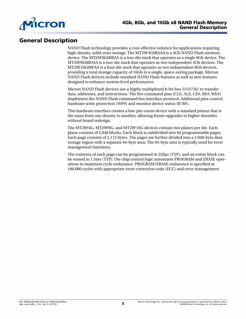
General DescriptionNAND Flash technology provides a cost-effective solution for applications requiring high-density, solid-state storage. The MT29F4G08AAA is a 4Gb NAND Flash memory device. The MT29F8G08BAA is a two-die stack that operates as a single 8Gb device. The MT29F8G08DAA is a two-die stack that operates as two independent 4Gb devices. The MT29F16G08FAA is a four-die stack that operates as two independent 8Gb devices, providing a total storage capacity of 16Gb in a single, space-saving package. Micron NAND Flash devices include standard NAND Flash features as well as new features designed to enhance system-level performance.
Micron NAND Flash devices use a highly multiplexed 8-bit bus (I/O[7:0]) to transfer data, addresses, and instructions. The five command pins (CLE, ALE, CE#, RE#, WE#) implement the NAND Flash command bus interface protocol. Additional pins control hardware write protection (WP#) and monitor device status (R/B#).
This hardware interface creates a low-pin-count device with a standard pinout that is the same from one density to another, allowing future upgrades to higher densities without board redesign.
The MT29F4G, MT29F8G, and MT29F16G devices contain two planes per die. Each plane consists of 2,048 blocks. Each block is subdivided into 64 programmable pages. Each page consists of 2,112 bytes. The pages are further divided into a 2,048-byte data storage region with a separate 64-byte area. The 64-byte area is typically used for error management functions.
The contents of each page can be programmed in 220µs (TYP), and an entire block can be erased in 1.5ms (TYP). On-chip control logic automates PROGRAM and ERASE oper-ations to maximize cycle endurance. PROGRAM/ERASE endurance is specified at 100,000 cycles with appropriate error correction code (ECC) and error management.
PDF: 09005aef81b80e13/Source: 09005aef81b80eac Micron Technology, Inc., reserves the right to change products or specifications without notice.4gb_nand_m40a__2.fm - Rev. B 2/07 EN 8 ©2006 Micron Technology, Inc. All rights reserved.
4Gb, 8Gb, and 16Gb x8 NAND Flash MemoryGeneral Description
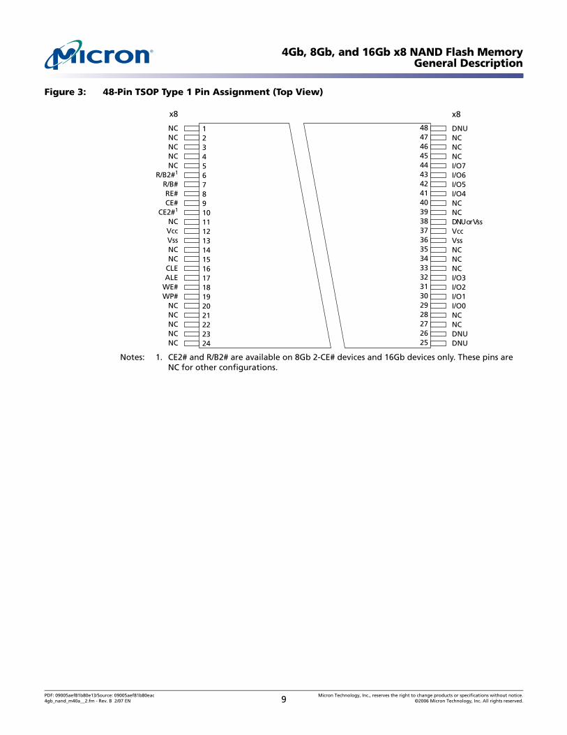
Figure 3: 48-Pin TSOP Type 1 Pin Assignment (Top View)
Notes: 1. CE2# and R/B2# are available on 8Gb 2-CE# devices and 16Gb devices only. These pins are NC for other configurations.
x8
NCNCNCNCNC
R/B2#1
R/B#RE#CE#
CE2#1
NCVccVssNCNC
CLEALE
WE#WP#
NCNCNCNCNC
x8
DNUNCNCNCI/O7I/O6I/O5I/O4NCNCDNU or VssVccVssNCNCNCI/O3I/O2I/O1I/O0NCNCDNUDNU
1 23456789101112131415161718192021222324
484746454443424140393837363534333231302928272625
PDF: 09005aef81b80e13/Source: 09005aef81b80eac Micron Technology, Inc., reserves the right to change products or specifications without notice.4gb_nand_m40a__2.fm - Rev. B 2/07 EN 9 ©2006 Micron Technology, Inc. All rights reserved.
4Gb, 8Gb, and 16Gb x8 NAND Flash MemoryGeneral Description
Table 1: Signal Descriptions
Symbol Type Description
ALE Input Address latch enable: During the time ALE is HIGH, address information is transferred from I/O[7:0] into the on-chip address register on the rising edge of WE#. When address information is not being loaded, ALE should be driven LOW.
CE#, CE2# Input Chip enable: Gates transfers between the host system and the NAND Flash device. After the device starts a PROGRAM or ERASE operation, CE# can be de-asserted. For the 8Gb configuration, CE# controls the first 4Gb of memory; CE2# controls the second 4Gb of memory. For the 16Gb configuration, CE# controls the first 8Gb of memory; CE2# controls the second 8Gb. See “Bus Operation” on page 15 for additional operational details.
CLE Input Command latch enable: When CLE is HIGH, information is transferred fromI/O[7:0] to the on-chip command register on the rising edge of WE#. When command information is not being loaded, CLE should be driven LOW.
RE# Input Read enable: Gates transfers from the NAND Flash device to the host system.WE# Input Write enable: Gates transfers from the host system to the NAND Flash device.WP# Input Write protect: Protects against inadvertent PROGRAM and ERASE operations. All
PROGRAM and ERASE operations are disabled when WP# is LOW.I/O[7:0]
(x8)I/O Data inputs/outputs: The bidirectional I/Os transfer address, data, and instruction
information. Data is output only during READ operations; at other times the I/Os are inputs.
R/B#, R/B2# Output Ready/busy: An open-drain, active-LOW output, that uses an external pull-up resistor. R/B# is used to indicate when the chip is processing a PROGRAM or ERASE operation. It is also used during READ operations to indicate when data is being transferred from the array into the serial data register. When these operations have completed, R/B# returns to the High-Z state. In the 8Gb configuration, R/B# is for the 4Gb of memory enabled by CE#; R/B2# is for the 4Gb of memory enabled by CE2#. In the 16Gb configuration, R/B# is for the 8Gb of memory enabled by CE#; R/B2# is for the 8Gb of memory enabled by CE2#.
VCC Supply VCC: Power supply.VSS Supply VSS: Ground connection.NC – No connect: NCs are not internally connected. They can be driven or left
unconnected.DNU – Do not use: DNUs must be left unconnected.
PDF: 09005aef81b80e13/Source: 09005aef81b80eac Micron Technology, Inc., reserves the right to change products or specifications without notice.4gb_nand_m40a__2.fm - Rev. B 2/07 EN 10 ©2006 Micron Technology, Inc. All rights reserved.
4Gb, 8Gb, and 16Gb x8 NAND Flash MemoryArchitecture
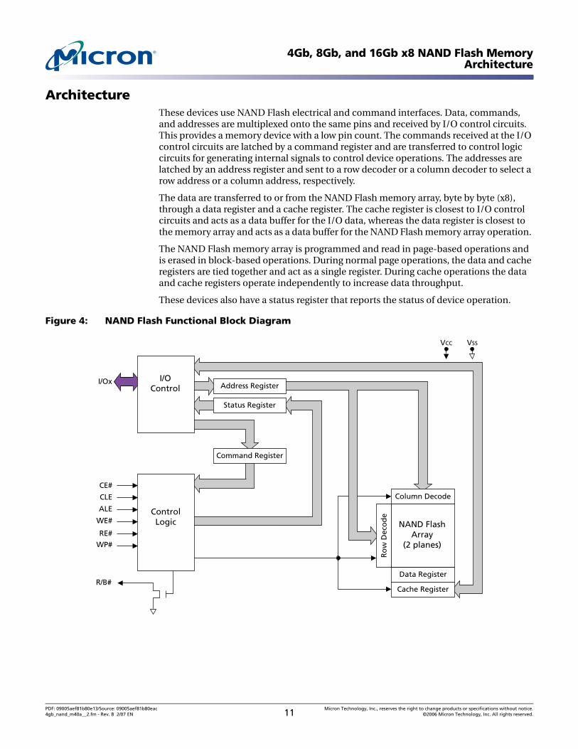
ArchitectureThese devices use NAND Flash electrical and command interfaces. Data, commands, and addresses are multiplexed onto the same pins and received by I/O control circuits. This provides a memory device with a low pin count. The commands received at the I/O control circuits are latched by a command register and are transferred to control logic circuits for generating internal signals to control device operations. The addresses are latched by an address register and sent to a row decoder or a column decoder to select a row address or a column address, respectively.
The data are transferred to or from the NAND Flash memory array, byte by byte (x8), through a data register and a cache register. The cache register is closest to I/O control circuits and acts as a data buffer for the I/O data, whereas the data register is closest to the memory array and acts as a data buffer for the NAND Flash memory array operation.
The NAND Flash memory array is programmed and read in page-based operations and is erased in block-based operations. During normal page operations, the data and cache registers are tied together and act as a single register. During cache operations the data and cache registers operate independently to increase data throughput.
These devices also have a status register that reports the status of device operation.
Figure 4: NAND Flash Functional Block Diagram
Address Register
Data Register
Cache Register
Status Register
Command Register
CE#
VCC VSS
CLE
ALE
WE#
RE#
WP#
I/Ox
ControlLogic
I/OControl
R/B#
Ro
w D
eco
de
Column Decode
NAND FlashArray
(2 planes)
PDF: 09005aef81b80e13/Source: 09005aef81b80eac Micron Technology, Inc., reserves the right to change products or specifications without notice.4gb_nand_m40a__2.fm - Rev. B 2/07 EN 11 ©2006 Micron Technology, Inc. All rights reserved.
4Gb, 8Gb, and 16Gb x8 NAND Flash MemoryAddressing
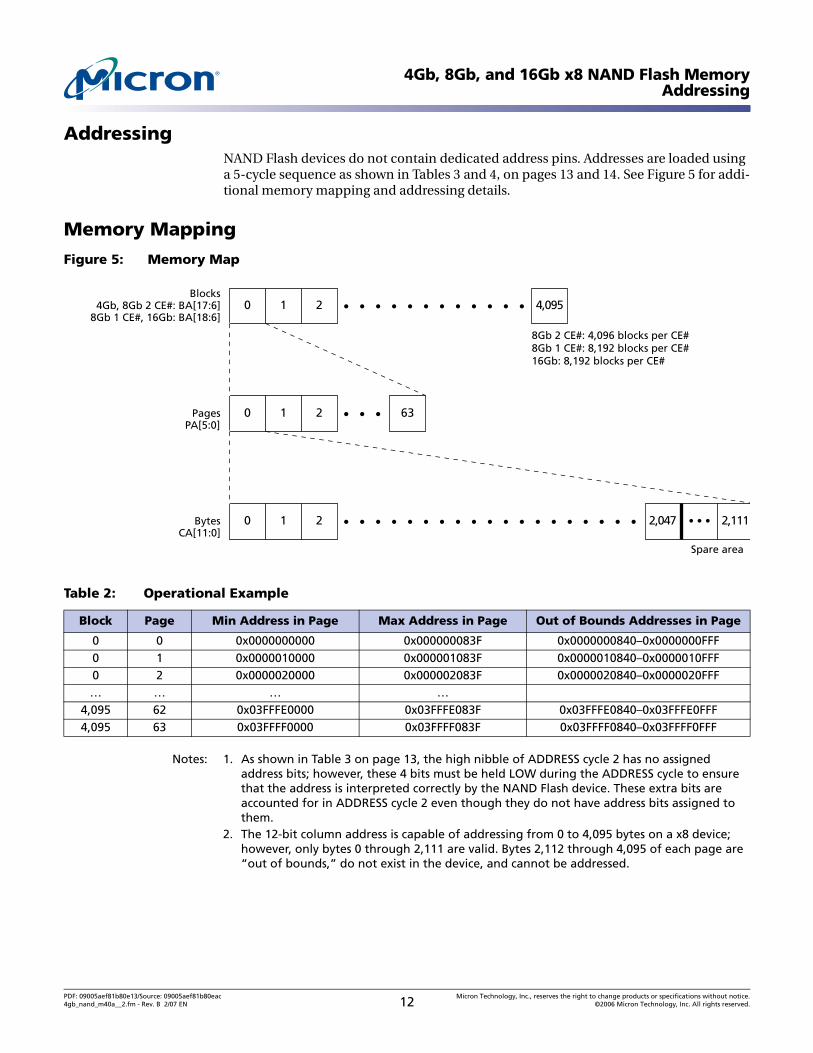
AddressingNAND Flash devices do not contain dedicated address pins. Addresses are loaded using a 5-cycle sequence as shown in Tables 3 and 4, on pages 13 and 14. See Figure 5 for addi-tional memory mapping and addressing details.
Memory Mapping
Figure 5: Memory Map
Notes: 1. As shown in Table 3 on page 13, the high nibble of ADDRESS cycle 2 has no assigned address bits; however, these 4 bits must be held LOW during the ADDRESS cycle to ensure that the address is interpreted correctly by the NAND Flash device. These extra bits are accounted for in ADDRESS cycle 2 even though they do not have address bits assigned to them.
2. The 12-bit column address is capable of addressing from 0 to 4,095 bytes on a x8 device; however, only bytes 0 through 2,111 are valid. Bytes 2,112 through 4,095 of each page are “out of bounds,” do not exist in the device, and cannot be addressed.
Table 2: Operational Example
Block Page Min Address in Page Max Address in Page Out of Bounds Addresses in Page
0 0 0x0000000000 0x000000083F 0x0000000840–0x0000000FFF0 1 0x0000010000 0x000001083F 0x0000010840–0x0000010FFF0 2 0x0000020000 0x000002083F 0x0000020840–0x0000020FFF… … … …
4,095 62 0x03FFFE0000 0x03FFFE083F 0x03FFFE0840–0x03FFFE0FFF4,095 63 0x03FFFF0000 0x03FFFF083F 0x03FFFF0840–0x03FFFF0FFF
• • • • • • • • • • • •
• • •
• • • • • • • • • • • • • • • • • • •
Blocks4Gb, 8Gb 2 CE#: BA[17:6]
8Gb 1 CE#, 16Gb: BA[18:6]
PagesPA[5:0]
BytesCA[11:0]
0 1 2
0 1 2 63
0 1 2 2,047 • • • 2,111
4,095
Spare area
8Gb 2 CE#: 4,096 blocks per CE#8Gb 1 CE#: 8,192 blocks per CE#16Gb: 8,192 blocks per CE#
PDF: 09005aef81b80e13/Source: 09005aef81b80eac Micron Technology, Inc., reserves the right to change products or specifications without notice.4gb_nand_m40a__2.fm - Rev. B 2/07 EN 12 ©2006 Micron Technology, Inc. All rights reserved.
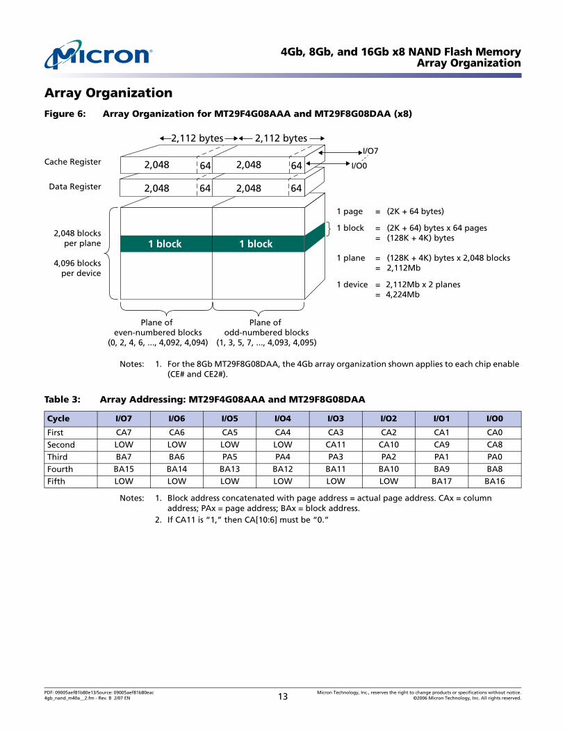
4Gb, 8Gb, and 16Gb x8 NAND Flash MemoryArray Organization
Array Organization
Figure 6: Array Organization for MT29F4G08AAA and MT29F8G08DAA (x8)
Notes: 1. For the 8Gb MT29F8G08DAA, the 4Gb array organization shown applies to each chip enable (CE# and CE2#).
Notes: 1. Block address concatenated with page address = actual page address. CAx = column address; PAx = page address; BAx = block address.
2. If CA11 is “1,” then CA[10:6] must be “0.”
Table 3: Array Addressing: MT29F4G08AAA and MT29F8G08DAA
Cycle I/O7 I/O6 I/O5 I/O4 I/O3 I/O2 I/O1 I/O0
First CA7 CA6 CA5 CA4 CA3 CA2 CA1 CA0
Second LOW LOW LOW LOW CA11 CA10 CA9 CA8
Third BA7 BA6 PA5 PA4 PA3 PA2 PA1 PA0
Fourth BA15 BA14 BA13 BA12 BA11 BA10 BA9 BA8
Fifth LOW LOW LOW LOW LOW LOW BA17 BA16
Cache Register
Data Register
2,048 blocksper plane
4,096 blocksper device
1 block 1 block
I/O0
I/O7
1 page = (2K + 64 bytes)
1 block = (2K + 64) bytes x 64 pages = (128K + 4K) bytes
1 plane = (128K + 4K) bytes x 2,048 blocks = 2,112Mb
1 device = 2,112Mb x 2 planes = 4,224Mb
Plane of even-numbered blocks
(0, 2, 4, 6, ..., 4,092, 4,094)
Plane of odd-numbered blocks
(1, 3, 5, 7, ..., 4,093, 4,095)
642,048 64
2,112 bytes2,112 bytes
64642,048
2,048
2,048
PDF: 09005aef81b80e13/Source: 09005aef81b80eac Micron Technology, Inc., reserves the right to change products or specifications without notice.4gb_nand_m40a__2.fm - Rev. B 2/07 EN 13 ©2006 Micron Technology, Inc. All rights reserved.
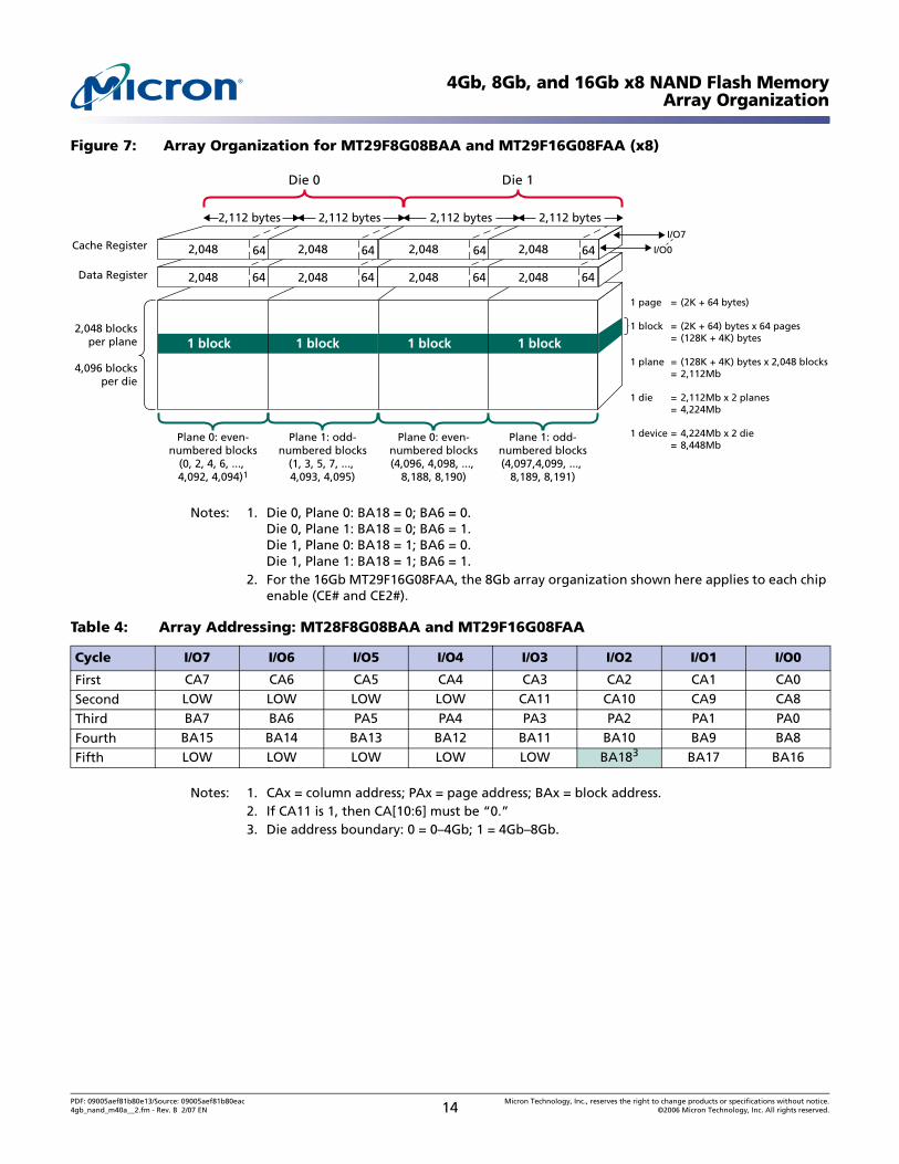
4Gb, 8Gb, and 16Gb x8 NAND Flash MemoryArray Organization
Figure 7: Array Organization for MT29F8G08BAA and MT29F16G08FAA (x8)
Notes: 1. Die 0, Plane 0: BA18 = 0; BA6 = 0.Die 0, Plane 1: BA18 = 0; BA6 = 1.Die 1, Plane 0: BA18 = 1; BA6 = 0.Die 1, Plane 1: BA18 = 1; BA6 = 1.
2. For the 16Gb MT29F16G08FAA, the 8Gb array organization shown here applies to each chip enable (CE# and CE2#).
Notes: 1. CAx = column address; PAx = page address; BAx = block address.2. If CA11 is 1, then CA[10:6] must be “0.”3. Die address boundary: 0 = 0–4Gb; 1 = 4Gb–8Gb.
Table 4: Array Addressing: MT28F8G08BAA and MT29F16G08FAA
Cycle I/O7 I/O6 I/O5 I/O4 I/O3 I/O2 I/O1 I/O0
First CA7 CA6 CA5 CA4 CA3 CA2 CA1 CA0
Second LOW LOW LOW LOW CA11 CA10 CA9 CA8
Third BA7 BA6 PA5 PA4 PA3 PA2 PA1 PA0
Fourth BA15 BA14 BA13 BA12 BA11 BA10 BA9 BA8
Fifth LOW LOW LOW LOW LOW BA183 BA17 BA16
Cache Register
Data Register
2,048 blocksper plane
4,096 blocksper die
1 block 1 block
Plane 0: even-numbered blocks
(0, 2, 4, 6, ..., 4,092, 4,094)1
Plane 1: odd-numbered blocks
(1, 3, 5, 7, ..., 4,093, 4,095)
Plane 0: even-numbered blocks(4,096, 4,098, ...,
8,188, 8,190)
Plane 1: odd-numbered blocks(4,097,4,099, ...,
8,189, 8,191)
642,048 64
2,112 bytes2,112 bytes
64642,048
2,048
2,048
1 block 1 block
642,048 64
2,112 bytes2,112 bytes
64642,048
2,048
2,048
1 page = (2K + 64 bytes)
1 block = (2K + 64) bytes x 64 pages = (128K + 4K) bytes
1 plane = (128K + 4K) bytes x 2,048 blocks = 2,112Mb
1 die = 2,112Mb x 2 planes = 4,224Mb
1 device = 4,224Mb x 2 die = 8,448Mb
I/O0
I/O7
Die 0 Die 1
PDF: 09005aef81b80e13/Source: 09005aef81b80eac Micron Technology, Inc., reserves the right to change products or specifications without notice.4gb_nand_m40a__2.fm - Rev. B 2/07 EN 14 ©2006 Micron Technology, Inc. All rights reserved.
4Gb, 8Gb, and 16Gb x8 NAND Flash MemoryBus Operation
Bus OperationThe bus on MT29Fxxx devices is multiplexed. Data I/O, addresses, and commands all share the same pins, I/O[7:0].
The command sequence normally consists of a COMMAND LATCH cycle, ADDRESS INPUT cycles, and 1 or more DATA cycles—either READ or WRITE.
Control Signals
CE#, WE#, RE#, CLE, ALE, and WP# control NAND Flash device READ and WRITE opera-tions. On the 8Gb MT29F8G08DAA, CE# and CE2# each control independent 4Gb arrays. On the 16Gb MT29F16G08FAA, CE# and CE2# each control independent 8Gb arrays. CE2# functions the same as CE# for its own array; all operations described for CE# also apply to CE2#.
CE# is used to enable the device. When CE# is LOW and the device is not in the busy state, the NAND Flash memory will accept command, address, and data information.
When the device is not performing an operation, the CE# pin is typically driven HIGH and the device enters standby mode. The memory will enter standby if CE# goes HIGH while data is being transferred and the device is not busy. This helps reduce power consumption. See Figure 61 on page 69 and Figure 69 on page 75 for examples of CE# “Don’t Care” operations.
The CE# “Don’t Care” operation enables the NAND Flash to reside on the same asyn-chronous memory bus as other Flash or SRAM devices. Other devices on the memory bus can then be accessed while the NAND Flash is busy with internal operations. This capability is important for designs that require multiple NAND Flash devices on the same bus.
A HIGH CLE signal indicates that a command cycle is taking place. A HIGH ALE signal signifies that an ADDRESS INPUT cycle is occurring.
Commands
Commands are written to the command register on the rising edge of WE# when:• CE# and ALE are LOW, and • CLE is HIGH, and • The device is not busy
As exceptions, the device accepts the READ STATUS, TWO-PLANE/MULTIPLE-DIE READ STATUS, and RESET commands when busy. Commands are transferred to the command register on the rising edge of WE# (see Figure 53 on page 65). Commands are input on I/O[7:0].
Address Input
Addresses are written to the address register on the rising edge of WE# when:• CE# and CLE are LOW, and• ALE is HIGH
Addresses are input on I/O[7:0]. Bits not part of the address space must be LOW.
The number of ADDRESS cycles required for each command varies. Refer to the command descriptions to determine addressing requirements (see Table 6 on page 19).
PDF: 09005aef81b80e13/Source: 09005aef81b80eac Micron Technology, Inc., reserves the right to change products or specifications without notice.4gb_nand_m40a__2.fm - Rev. B 2/07 EN 15 ©2006 Micron Technology, Inc. All rights reserved.
4Gb, 8Gb, and 16Gb x8 NAND Flash MemoryBus Operation
Data Input
Data is written to the data register on the rising edge of WE# when:• CE#, CLE, and ALE are LOW, and• the device is not busy
Data is input on I/O[7:0]. See Figure 55 on page 66 for additional data input details.
READs
After a READ command is issued, data is transferred from the memory array to the data register on the rising edge of WE#. R/B# goes LOW for tR and transitions HIGH after the transfer is complete. When data is available in the data register, it is clocked out of the part by RE# going LOW. See Figure 60 on page 68 for detailed timing information.
The READ STATUS (70h) command, TWO-PLANE/MULTIPLE-DIE READ STATUS (78h) command, or the R/B# signal can be used to determine when the device is ready.
If a controller is using a timing of 30ns or longer for tRC, use Figure 56 on page 66 for proper timing. If tRC is less than 30ns, use Figure 57 on page 67 for extended data output (EDO) timing.
Ready/Busy#
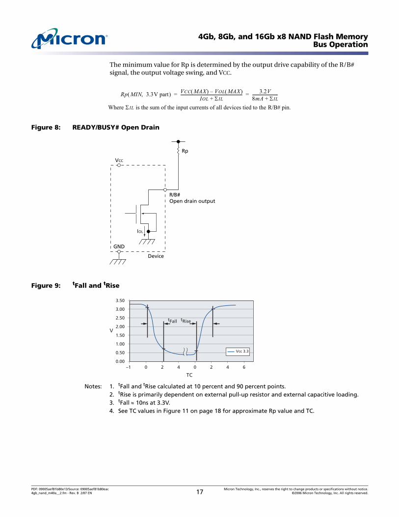
The R/B# output provides a hardware method of indicating the completion of PROGRAM, ERASE, and READ operations. The signal requires a pull-up resistor for proper operation. The signal is typically HIGH, and transitions to LOW after the appro-priate command is written to the device. The signal pin’s open-drain driver enables multiple R/B# outputs to be OR-tied. The READ STATUS command can be used in place of R/B#. Typically, R/B# is connected to an interrupt pin on the system controller (see Figure 8 on page 17).
On the 8Gb MT29F8G08DAA, R/B# provides a status indication for the 4Gb section enabled by CE#, and R/B2# does the same for the 4Gb section enabled by CE2#. R/B# and R/B2# can be tied together, or they can be used separately to provide independent indications for each 4Gb section.
On the 16Gb MT29F16G08FAA, R/B# provides a status indication for the 8Gb section enabled by CE#, and R/B2# does the same for the 8Gb section enabled by CE2#. R/B# and R/B2# can be tied together, or they can be used separately to provide independent indications for each 8Gb section.
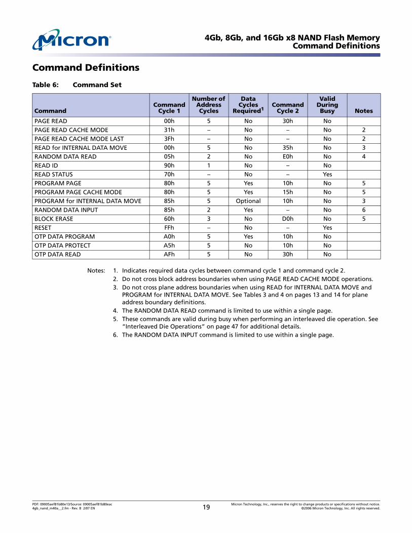
The combination of Rp and capacitive loading of the R/B# circuit determines the rise time of the R/B# pin. The actual value used for Rp depends on the system timing requirements. Large values of Rp cause R/B# to be delayed significantly. At the 10 to 90 percent points on the R/B# waveform, rise time is approximately two time constants (TC).
The fall time of the R/B# signal is determined mainly by the output impedance of the R/B# pin and the total load capacitance.
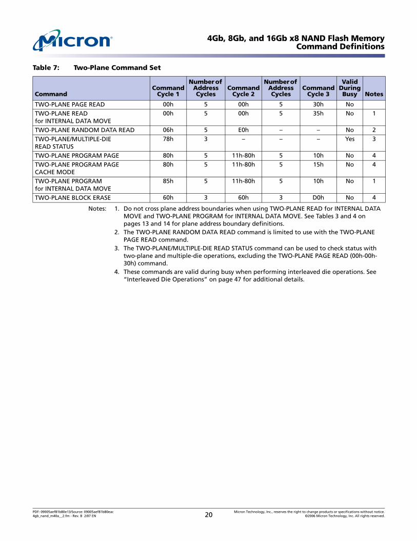
Refer to Figures 10 and 11 on page 18, which depict approximate Rp values using a circuit load of 100pF.
TC R C×=Where R = Rp (resistance of pull-up resistor), and C = total capacitive load.
PDF: 09005aef81b80e13/Source: 09005aef81b80eac Micron Technology, Inc., reserves the right to change products or specifications without notice.4gb_nand_m40a__2.fm - Rev. B 2/07 EN 16 ©2006 Micron Technology, Inc. All rights reserved.
4Gb, 8Gb, and 16Gb x8 NAND Flash MemoryBus Operation
The minimum value for Rp is determined by the output drive capability of the R/B# signal, the output voltage swing, and VCC.
Figure 8: READY/BUSY# Open Drain
Figure 9: tFall and tRise
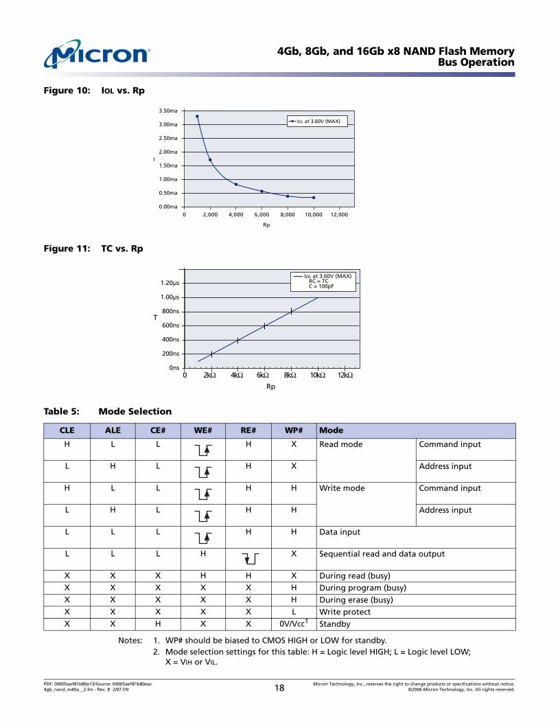
Notes: 1. tFall and tRise calculated at 10 percent and 90 percent points.2. tRise is primarily dependent on external pull-up resistor and external capacitive loading.3. tFall ≈ 10ns at 3.3V.4. See TC values in Figure 11 on page 18 for approximate Rp value and TC.
Rp MIN 3.3V part,( ) VCC MAX( ) VOL MAX( )–IOL ΣIL+
--------------------------------------------------------------- 3.2V8mA ΣIL+--------------------------= =
Where ΣIL is the sum of the input currents of all devices tied to the R/B# pin.
Rp
R/B#Open drain output
VCC
GND
Device
IOL
3.50
3.00
2.50
2.00
1.50
1.00
0.50
0.00–1 0 2 4 0 2 4 6
tFall tRise
TC
V
Vcc 3.3
PDF: 09005aef81b80e13/Source: 09005aef81b80eac Micron Technology, Inc., reserves the right to change products or specifications without notice.4gb_nand_m40a__2.fm - Rev. B 2/07 EN 17 ©2006 Micron Technology, Inc. All rights reserved.
4Gb, 8Gb, and 16Gb x8 NAND Flash MemoryBus Operation
Figure 10: IOL vs. Rp
Figure 11: TC vs. Rp
Notes: 1. WP# should be biased to CMOS HIGH or LOW for standby.2. Mode selection settings for this table: H = Logic level HIGH; L = Logic level LOW;
X = VIH or VIL.
Table 5: Mode Selection
CLE ALE CE# WE# RE# WP# Mode
H L L H X Read mode Command input
L H L H X Address input
H L L H H Write mode Command input
L H L H H Address input
L L L H H Data input
L L L H X Sequential read and data output
X X X H H X During read (busy)X X X X X H During program (busy)X X X X X H During erase (busy)X X X X X L Write protectX X H X X 0V/Vcc1 Standby
3.50ma
3.00ma
2.50ma
2.00ma
1.50ma
1.00ma
0.50ma
0.00ma0 2,000 4,000 6,000 8,000 10,000 12,000
Rp
I
IOL at 3.60V (MAX)
1.20µs
1.00µs
800ns
600ns
400ns
200ns
0ns0 2kΩ 4kΩ 6kΩ 8kΩ 10kΩ 12kΩ
Rp
T
IOL at 3.60V (MAX) RC = TC C = 100pF
PDF: 09005aef81b80e13/Source: 09005aef81b80eac Micron Technology, Inc., reserves the right to change products or specifications without notice.4gb_nand_m40a__2.fm - Rev. B 2/07 EN 18 ©2006 Micron Technology, Inc. All rights reserved.
4Gb, 8Gb, and 16Gb x8 NAND Flash MemoryCommand Definitions
Command Definitions
Notes: 1. Indicates required data cycles between command cycle 1 and command cycle 2.2. Do not cross block address boundaries when using PAGE READ CACHE MODE operations.3. Do not cross plane address boundaries when using READ for INTERNAL DATA MOVE and
PROGRAM for INTERNAL DATA MOVE. See Tables 3 and 4 on pages 13 and 14 for plane address boundary definitions.
4. The RANDOM DATA READ command is limited to use within a single page.5. These commands are valid during busy when performing an interleaved die operation. See
“Interleaved Die Operations” on page 47 for additional details.6. The RANDOM DATA INPUT command is limited to use within a single page.
Table 6: Command Set
CommandCommand
Cycle 1
Number of Address Cycles
Data Cycles
Required1Command
Cycle 2
Valid During Busy Notes
PAGE READ 00h 5 No 30h No
PAGE READ CACHE MODE 31h – No – No 2
PAGE READ CACHE MODE LAST 3Fh – No – No 2
READ for INTERNAL DATA MOVE 00h 5 No 35h No 3
RANDOM DATA READ 05h 2 No E0h No 4
READ ID 90h 1 No – No
READ STATUS 70h – No – Yes
PROGRAM PAGE 80h 5 Yes 10h No 5
PROGRAM PAGE CACHE MODE 80h 5 Yes 15h No 5
PROGRAM for INTERNAL DATA MOVE 85h 5 Optional 10h No 3
RANDOM DATA INPUT 85h 2 Yes – No 6
BLOCK ERASE 60h 3 No D0h No 5
RESET FFh – No – Yes
OTP DATA PROGRAM A0h 5 Yes 10h No
OTP DATA PROTECT A5h 5 No 10h No
OTP DATA READ AFh 5 No 30h No
PDF: 09005aef81b80e13/Source: 09005aef81b80eac Micron Technology, Inc., reserves the right to change products or specifications without notice.4gb_nand_m40a__2.fm - Rev. B 2/07 EN 19 ©2006 Micron Technology, Inc. All rights reserved.
4Gb, 8Gb, and 16Gb x8 NAND Flash MemoryCommand Definitions
Notes: 1. Do not cross plane address boundaries when using TWO-PLANE READ for INTERNAL DATA MOVE and TWO-PLANE PROGRAM for INTERNAL DATA MOVE. See Tables 3 and 4 on pages 13 and 14 for plane address boundary definitions.
2. The TWO-PLANE RANDOM DATA READ command is limited to use with the TWO-PLANE PAGE READ command.
3. The TWO-PLANE/MULTIPLE-DIE READ STATUS command can be used to check status with two-plane and multiple-die operations, excluding the TWO-PLANE PAGE READ (00h-00h-30h) command.
4. These commands are valid during busy when performing interleaved die operations. See “Interleaved Die Operations” on page 47 for additional details.
Table 7: Two-Plane Command Set
CommandCommand
Cycle 1
Number of Address Cycles
Command Cycle 2
Number of Address Cycles
Command Cycle 3
Valid During Busy Notes
TWO-PLANE PAGE READ 00h 5 00h 5 30h No
TWO-PLANE READfor INTERNAL DATA MOVE
00h 5 00h 5 35h No 1
TWO-PLANE RANDOM DATA READ 06h 5 E0h – – No 2
TWO-PLANE/MULTIPLE-DIEREAD STATUS
78h 3 – – – Yes 3
TWO-PLANE PROGRAM PAGE 80h 5 11h-80h 5 10h No 4
TWO-PLANE PROGRAM PAGE CACHE MODE
80h 5 11h-80h 5 15h No 4
TWO-PLANE PROGRAM for INTERNAL DATA MOVE
85h 5 11h-80h 5 10h No 1
TWO-PLANE BLOCK ERASE 60h 3 60h 3 D0h No 4
PDF: 09005aef81b80e13/Source: 09005aef81b80eac Micron Technology, Inc., reserves the right to change products or specifications without notice.4gb_nand_m40a__2.fm - Rev. B 2/07 EN 20 ©2006 Micron Technology, Inc. All rights reserved.
4Gb, 8Gb, and 16Gb x8 NAND Flash MemoryCommand Definitions
READ Operations
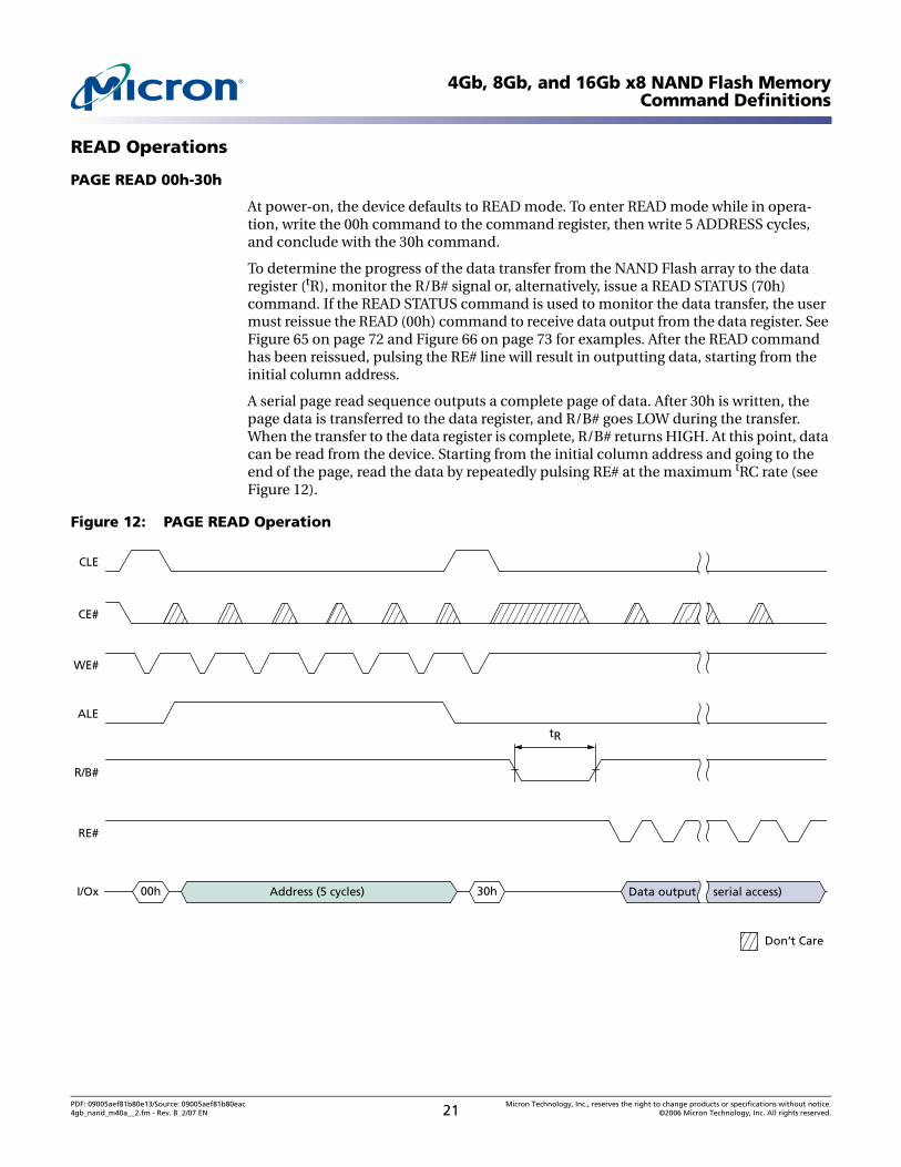
PAGE READ 00h-30h
At power-on, the device defaults to READ mode. To enter READ mode while in opera-tion, write the 00h command to the command register, then write 5 ADDRESS cycles, and conclude with the 30h command.
To determine the progress of the data transfer from the NAND Flash array to the data register (tR), monitor the R/B# signal or, alternatively, issue a READ STATUS (70h) command. If the READ STATUS command is used to monitor the data transfer, the user must reissue the READ (00h) command to receive data output from the data register. See Figure 65 on page 72 and Figure 66 on page 73 for examples. After the READ command has been reissued, pulsing the RE# line will result in outputting data, starting from the initial column address.
A serial page read sequence outputs a complete page of data. After 30h is written, the page data is transferred to the data register, and R/B# goes LOW during the transfer. When the transfer to the data register is complete, R/B# returns HIGH. At this point, data can be read from the device. Starting from the initial column address and going to the end of the page, read the data by repeatedly pulsing RE# at the maximum tRC rate (see Figure 12).
Figure 12: PAGE READ Operation
RE#
CE#
ALE
CLE
I/Ox 00h Address (5 cycles) Data output ( serial access)30h
R/B#
WE#
tR
Don’t Care
PDF: 09005aef81b80e13/Source: 09005aef81b80eac Micron Technology, Inc., reserves the right to change products or specifications without notice.4gb_nand_m40a__2.fm - Rev. B 2/07 EN 21 ©2006 Micron Technology, Inc. All rights reserved.
4Gb, 8Gb, and 16Gb x8 NAND Flash MemoryCommand Definitions
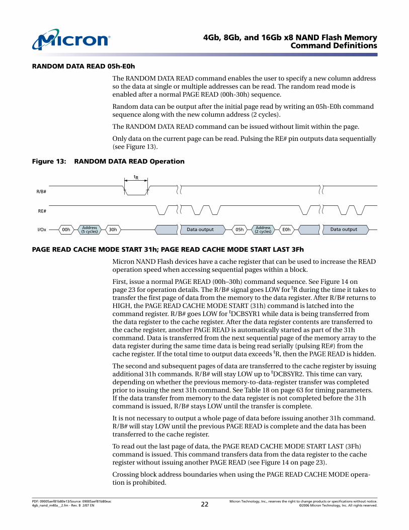
RANDOM DATA READ 05h-E0h
The RANDOM DATA READ command enables the user to specify a new column address so the data at single or multiple addresses can be read. The random read mode is enabled after a normal PAGE READ (00h-30h) sequence.
Random data can be output after the initial page read by writing an 05h-E0h command sequence along with the new column address (2 cycles).
The RANDOM DATA READ command can be issued without limit within the page.
Only data on the current page can be read. Pulsing the RE# pin outputs data sequentially (see Figure 13).
Figure 13: RANDOM DATA READ Operation
PAGE READ CACHE MODE START 31h; PAGE READ CACHE MODE START LAST 3Fh
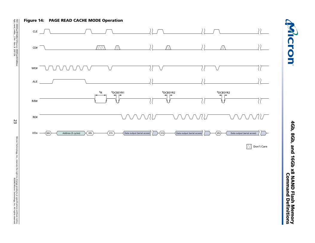
Micron NAND Flash devices have a cache register that can be used to increase the READ operation speed when accessing sequential pages within a block.
First, issue a normal PAGE READ (00h–30h) command sequence. See Figure 14 on page 23 for operation details. The R/B# signal goes LOW for tR during the time it takes to transfer the first page of data from the memory to the data register. After R/B# returns to HIGH, the PAGE READ CACHE MODE START (31h) command is latched into the command register. R/B# goes LOW for tDCBSYR1 while data is being transferred from the data register to the cache register. After the data register contents are transferred to the cache register, another PAGE READ is automatically started as part of the 31h command. Data is transferred from the next sequential page of the memory array to the data register during the same time data is being read serially (pulsing RE#) from the cache register. If the total time to output data exceeds tR, then the PAGE READ is hidden.
The second and subsequent pages of data are transferred to the cache register by issuing additional 31h commands. R/B# will stay LOW up to tDCBSYR2. This time can vary, depending on whether the previous memory-to-data-register transfer was completed prior to issuing the next 31h command. See Table 18 on page 63 for timing parameters. If the data transfer from memory to the data register is not completed before the 31h command is issued, R/B# stays LOW until the transfer is complete.
It is not necessary to output a whole page of data before issuing another 31h command. R/B# will stay LOW until the previous PAGE READ is complete and the data has been transferred to the cache register.
To read out the last page of data, the PAGE READ CACHE MODE START LAST (3Fh) command is issued. This command transfers data from the data register to the cache register without issuing another PAGE READ (see Figure 14 on page 23).
Crossing block address boundaries when using the PAGE READ CACHE MODE opera-tion is prohibited.
RE#
I/Ox 00h Address(5 cycles) Data output Data output30h 05h Address
(2 cycles) E0h
R/B#
tR
PDF: 09005aef81b80e13/Source: 09005aef81b80eac Micron Technology, Inc., reserves the right to change products or specifications without notice.4gb_nand_m40a__2.fm - Rev. B 2/07 EN 22 ©2006 Micron Technology, Inc. All rights reserved.
PDF: 09005aef81b
4gb
_nan
d_m
40a__2.fm-
Rev. B
2/07 EN23
©2006 M
icron
Techn
olo
gy, In
c. All rig
hts reserved
.
4Gb
, 8Gb
, and
16Gb
x8 NA
ND
Flash M
emo
ryC
om
man
d D
efinitio
ns
Figure 14: PAGE READ CACHE MODE Operation
CLE
Data output (serial access)
2
Don’t Care
80e13/Sou
rce: 09005aef81b80eac
Micro
n Tech
no
log
y, Inc., reserves th
e righ
t to ch
ang
e pro
du
cts or sp
ecification
s with
ou
t no
tice.
RE#
CE#
ALE
I/Ox 00h Address (5 cycles) Data output (serial access) Data output (serial access)31h30h 31h 3Fh
R/B#
WE#
tR tDCBSYR1 tDCBSYR2 tDCBSYR
4Gb, 8Gb, and 16Gb x8 NAND Flash MemoryCommand Definitions
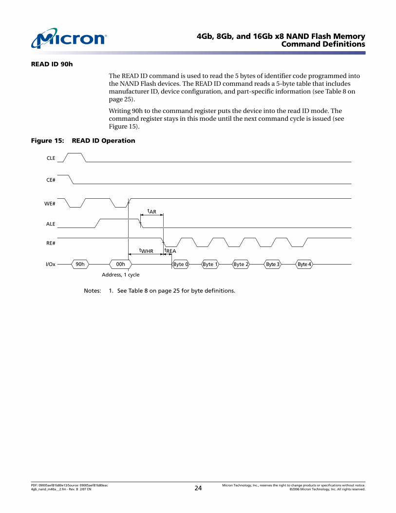
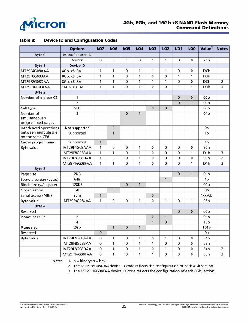
READ ID 90h
The READ ID command is used to read the 5 bytes of identifier code programmed into the NAND Flash devices. The READ ID command reads a 5-byte table that includes manufacturer ID, device configuration, and part-specific information (see Table 8 on page 25).
Writing 90h to the command register puts the device into the read ID mode. The command register stays in this mode until the next command cycle is issued (see Figure 15).
Figure 15: READ ID Operation
Notes: 1. See Table 8 on page 25 for byte definitions.
WE#
CE#
ALE
CLE
RE#
I/Ox
Address, 1 cycle
90h 00h Byte 2Byte 0 Byte 1 Byte 3 Byte 4
tAR
tREAtWHR
PDF: 09005aef81b80e13/Source: 09005aef81b80eac Micron Technology, Inc., reserves the right to change products or specifications without notice.4gb_nand_m40a__2.fm - Rev. B 2/07 EN 24 ©2006 Micron Technology, Inc. All rights reserved.
4Gb, 8Gb, and 16Gb x8 NAND Flash MemoryCommand Definitions
Notes: 1. b = binary; h = hex.2. The MT29F8G08DAA device ID code reflects the configuration of each 4Gb section.3. The MT29F16G08FAA device ID code reflects the configuration of each 8Gb section.
Table 8: Device ID and Configuration Codes
Options I/O7 I/O6 I/O5 I/O4 I/O3 I/O2 I/O1 I/O0 Value1 Notes
Byte 0 Manufacturer IDMicron 0 0 1 0 1 1 0 0 2Ch
Byte 1 Device IDMT29F4G08AAA 4Gb, x8, 3V 1 1 0 1 1 1 0 0 DCh
MT29F8G08BAA 8Gb, x8, 3V 1 1 0 1 0 0 1 1 D3h
MT29F8G08DAA 8Gb, x8, 3V 1 1 0 1 1 1 0 0 DCh 2
MT29F16G08FAA 16Gb, x8, 3V 1 1 0 1 0 0 1 1 D3h 3Byte 2
Number of die per CE 1 0 0 00b2 0 1 01b
Cell type SLC 0 0 00b
Number of simultaneously programmed pages
2 0 1 01b
Interleaved operations between multiple die on the same CE#
Not supported 0 0bSupported 1 1b
Cache programming Supported 1 1b
Byte value MT29F4G08AAA 1 0 0 1 0 0 0 0 90hMT29F8G08BAA 1 1 0 1 0 0 0 1 D1h 3MT29F8G08DAA 1 0 0 1 0 0 0 0 90h 2MT29F16G08FAA 1 1 0 1 0 0 0 1 D1h 3
Byte 3Page size 2KB 0 1 01b
Spare area size (bytes) 64B 1 1b
Block size (w/o spare) 128KB 0 1 01b
Organization x8 0 0b
Serial access (MIN) 25ns 1 0 1xxx0b
Byte value MT29FxG08xAA 1 0 0 1 0 1 0 1 95hByte 4
Reserved 0 0 00b
Planes per CE# 2 0 1 01b4 1 0 10b
Plane size 2Gb 1 0 1 101b
Reserved 0 0b
Byte value MT29F4G08AAA 0 1 0 1 0 1 0 0 54hMT29F8G08BAA 0 1 0 1 1 0 0 0 58hMT29F8G08DAA 0 1 0 1 0 1 0 0 54h 2MT29F16G08FAA 0 1 0 1 1 0 0 0 58h 3
PDF: 09005aef81b80e13/Source: 09005aef81b80eac Micron Technology, Inc., reserves the right to change products or specifications without notice.4gb_nand_m40a__2.fm - Rev. B 2/07 EN 25 ©2006 Micron Technology, Inc. All rights reserved.
4Gb, 8Gb, and 16Gb x8 NAND Flash MemoryCommand Definitions
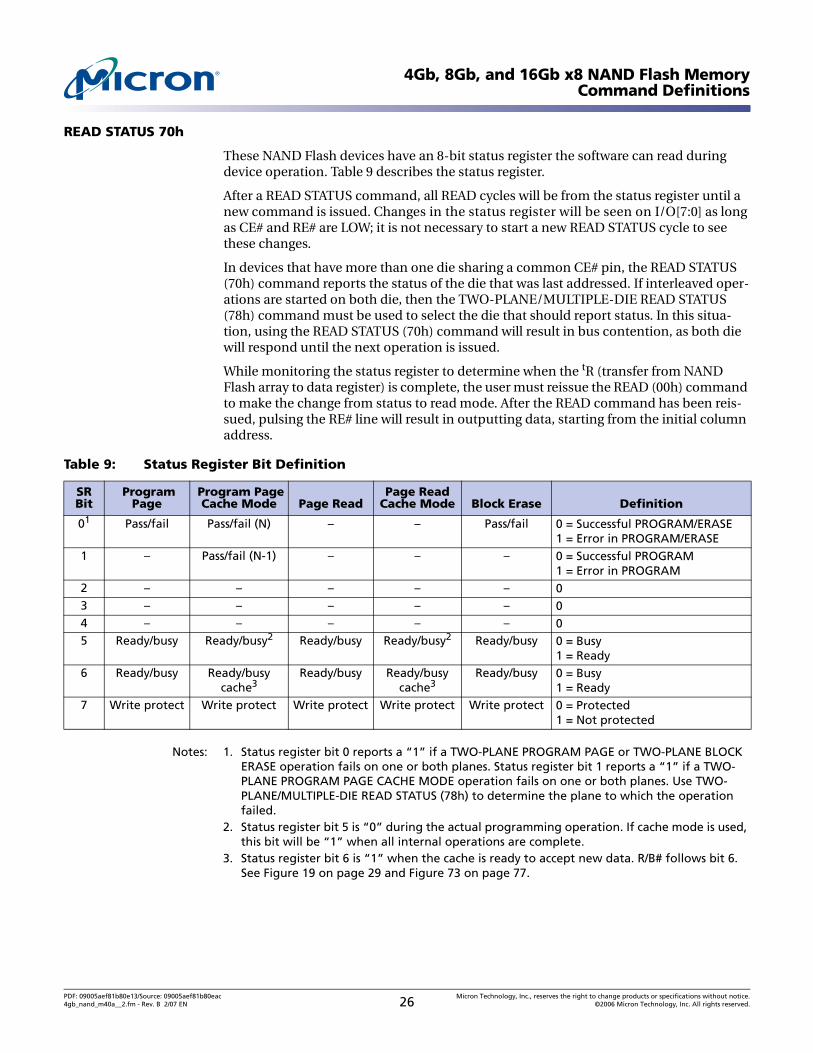
READ STATUS 70h
These NAND Flash devices have an 8-bit status register the software can read during device operation. Table 9 describes the status register.
After a READ STATUS command, all READ cycles will be from the status register until a new command is issued. Changes in the status register will be seen on I/O[7:0] as long as CE# and RE# are LOW; it is not necessary to start a new READ STATUS cycle to see these changes.
In devices that have more than one die sharing a common CE# pin, the READ STATUS (70h) command reports the status of the die that was last addressed. If interleaved oper-ations are started on both die, then the TWO-PLANE/MULTIPLE-DIE READ STATUS (78h) command must be used to select the die that should report status. In this situa-tion, using the READ STATUS (70h) command will result in bus contention, as both die will respond until the next operation is issued.
While monitoring the status register to determine when the tR (transfer from NAND Flash array to data register) is complete, the user must reissue the READ (00h) command to make the change from status to read mode. After the READ command has been reis-sued, pulsing the RE# line will result in outputting data, starting from the initial column address.
Notes: 1. Status register bit 0 reports a “1” if a TWO-PLANE PROGRAM PAGE or TWO-PLANE BLOCK ERASE operation fails on one or both planes. Status register bit 1 reports a “1” if a TWO-PLANE PROGRAM PAGE CACHE MODE operation fails on one or both planes. Use TWO-PLANE/MULTIPLE-DIE READ STATUS (78h) to determine the plane to which the operation failed.
2. Status register bit 5 is “0” during the actual programming operation. If cache mode is used, this bit will be “1” when all internal operations are complete.
3. Status register bit 6 is “1” when the cache is ready to accept new data. R/B# follows bit 6. See Figure 19 on page 29 and Figure 73 on page 77.
Table 9: Status Register Bit Definition
SRBit
Program Page
Program PageCache Mode Page Read
Page Read Cache Mode Block Erase Definition
01 Pass/fail Pass/fail (N) – – Pass/fail 0 = Successful PROGRAM/ERASE1 = Error in PROGRAM/ERASE
1 – Pass/fail (N-1) – – – 0 = Successful PROGRAM1 = Error in PROGRAM
2 – – – – – 03 – – – – – 04 – – – – – 05 Ready/busy Ready/busy2 Ready/busy Ready/busy2 Ready/busy 0 = Busy
1 = Ready6 Ready/busy Ready/busy
cache3Ready/busy Ready/busy
cache3Ready/busy 0 = Busy
1 = Ready7 Write protect Write protect Write protect Write protect Write protect 0 = Protected
1 = Not protected
PDF: 09005aef81b80e13/Source: 09005aef81b80eac Micron Technology, Inc., reserves the right to change products or specifications without notice.4gb_nand_m40a__2.fm - Rev. B 2/07 EN 26 ©2006 Micron Technology, Inc. All rights reserved.
4Gb, 8Gb, and 16Gb x8 NAND Flash MemoryCommand Definitions
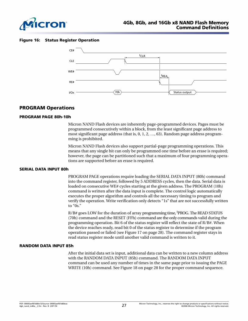
Figure 16: Status Register Operation
PROGRAM Operations
PROGRAM PAGE 80h-10h
Micron NAND Flash devices are inherently page-programmed devices. Pages must be programmed consecutively within a block, from the least significant page address to most significant page address (that is, 0, 1, 2, …, 63). Random page address program-ming is prohibited.
Micron NAND Flash devices also support partial-page programming operations. This means that any single bit can only be programmed one time before an erase is required; however, the page can be partitioned such that a maximum of four programming opera-tions are supported before an erase is required.
SERIAL DATA INPUT 80h
PROGRAM PAGE operations require loading the SERIAL DATA INPUT (80h) command into the command register, followed by 5 ADDRESS cycles, then the data. Serial data is loaded on consecutive WE# cycles starting at the given address. The PROGRAM (10h) command is written after the data input is complete. The control logic automatically executes the proper algorithm and controls all the necessary timing to program and verify the operation. Write verification only detects “1s” that are not successfully written to “0s.”
R/B# goes LOW for the duration of array programming time, tPROG. The READ STATUS (70h) command and the RESET (FFh) command are the only commands valid during the programming operation. Bit 6 of the status register will reflect the state of R/B#. When the device reaches ready, read bit 0 of the status register to determine if the program operation passed or failed (see Figure 17 on page 28). The command register stays in read status register mode until another valid command is written to it.
RANDOM DATA INPUT 85h
After the initial data set is input, additional data can be written to a new column address with the RANDOM DATA INPUT (85h) command. The RANDOM DATA INPUT command can be used any number of times in the same page prior to issuing the PAGE WRITE (10h) command. See Figure 18 on page 28 for the proper command sequence.
70h
CE#
CLE
WE#
RE#
I/Ox Status output
tREA
tCLR
PDF: 09005aef81b80e13/Source: 09005aef81b80eac Micron Technology, Inc., reserves the right to change products or specifications without notice.4gb_nand_m40a__2.fm - Rev. B 2/07 EN 27 ©2006 Micron Technology, Inc. All rights reserved.
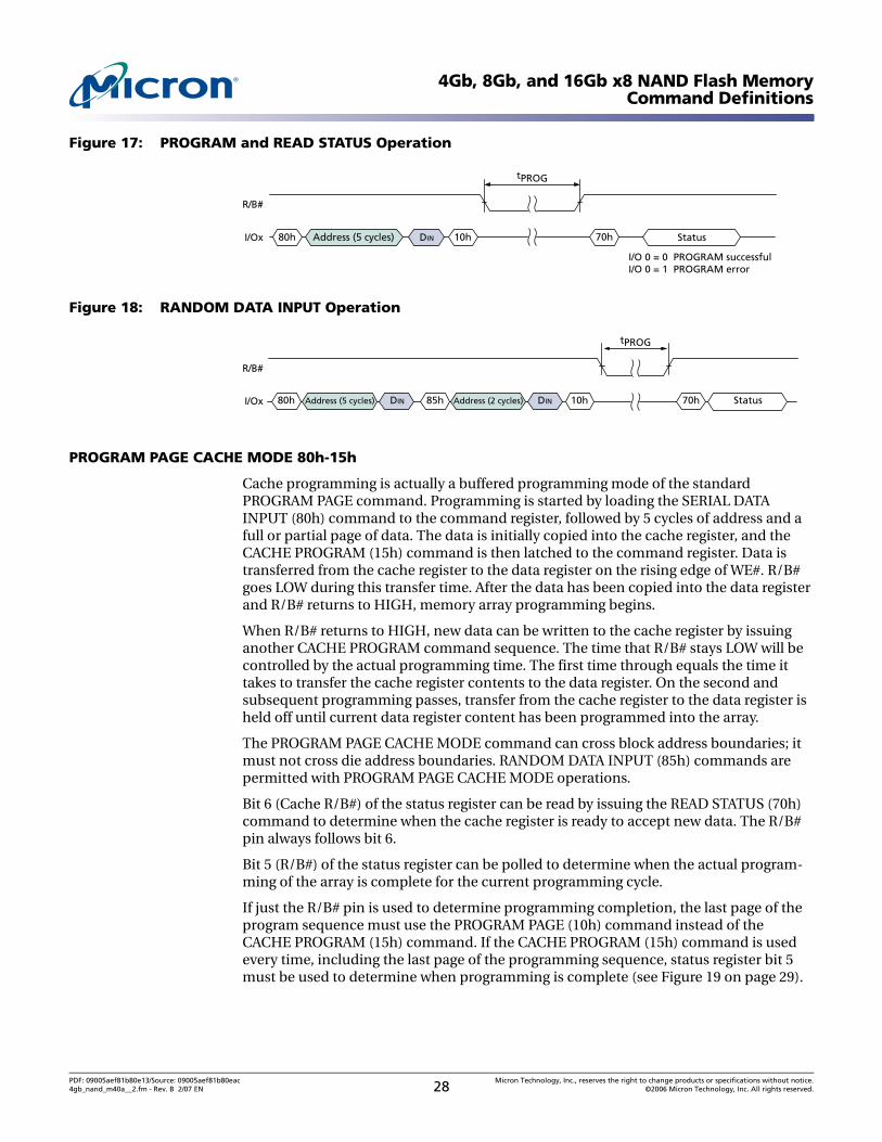
4Gb, 8Gb, and 16Gb x8 NAND Flash MemoryCommand Definitions
Figure 17: PROGRAM and READ STATUS Operation
Figure 18: RANDOM DATA INPUT Operation
PROGRAM PAGE CACHE MODE 80h-15h
Cache programming is actually a buffered programming mode of the standard PROGRAM PAGE command. Programming is started by loading the SERIAL DATA INPUT (80h) command to the command register, followed by 5 cycles of address and a full or partial page of data. The data is initially copied into the cache register, and the CACHE PROGRAM (15h) command is then latched to the command register. Data is transferred from the cache register to the data register on the rising edge of WE#. R/B# goes LOW during this transfer time. After the data has been copied into the data register and R/B# returns to HIGH, memory array programming begins.
When R/B# returns to HIGH, new data can be written to the cache register by issuing another CACHE PROGRAM command sequence. The time that R/B# stays LOW will be controlled by the actual programming time. The first time through equals the time it takes to transfer the cache register contents to the data register. On the second and subsequent programming passes, transfer from the cache register to the data register is held off until current data register content has been programmed into the array.
The PROGRAM PAGE CACHE MODE command can cross block address boundaries; it must not cross die address boundaries. RANDOM DATA INPUT (85h) commands are permitted with PROGRAM PAGE CACHE MODE operations.
Bit 6 (Cache R/B#) of the status register can be read by issuing the READ STATUS (70h) command to determine when the cache register is ready to accept new data. The R/B# pin always follows bit 6.
Bit 5 (R/B#) of the status register can be polled to determine when the actual program-ming of the array is complete for the current programming cycle.
If just the R/B# pin is used to determine programming completion, the last page of the program sequence must use the PROGRAM PAGE (10h) command instead of the CACHE PROGRAM (15h) command. If the CACHE PROGRAM (15h) command is used every time, including the last page of the programming sequence, status register bit 5 must be used to determine when programming is complete (see Figure 19 on page 29).
I/Ox 80h Address (5 cycles) 10h 70h
R/B#
tPROG
Status
I/O 0 = 0 PROGRAM successfulI/O 0 = 1 PROGRAM error
DIN
I/Ox 80h Address (5 cycles) 85h Address (2 cycles) 10h 70h
R/B#
tPROG
DINDIN Status
PDF: 09005aef81b80e13/Source: 09005aef81b80eac Micron Technology, Inc., reserves the right to change products or specifications without notice.4gb_nand_m40a__2.fm - Rev. B 2/07 EN 28 ©2006 Micron Technology, Inc. All rights reserved.
4Gb, 8Gb, and 16Gb x8 NAND Flash MemoryCommand Definitions
Bit 0 of the status register returns the pass/fail for the previous page when bit 6 of the status register is a “1” (ready state). The pass/fail status of the current PROGRAM opera-tion is returned with bit 0 of the status register when bit 5 of the status register is a “1” (ready state) as shown in Figure 19.
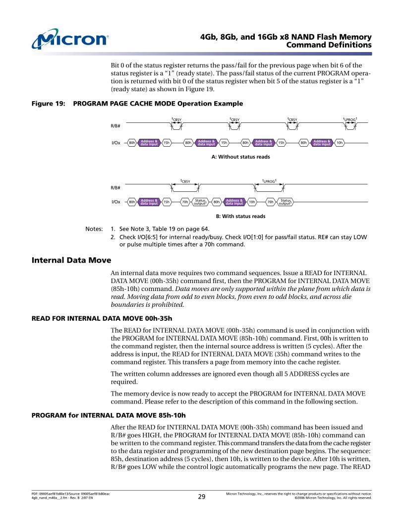
Figure 19: PROGRAM PAGE CACHE MODE Operation Example
Notes: 1. See Note 3, Table 19 on page 64.2. Check I/O[6:5] for internal ready/busy. Check I/O[1:0] for pass/fail status. RE# can stay LOW
or pulse multiple times after a 70h command.
Internal Data Move
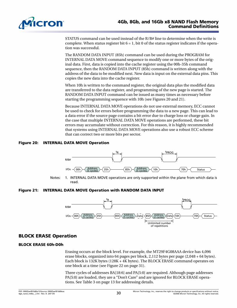
An internal data move requires two command sequences. Issue a READ for INTERNAL DATA MOVE (00h-35h) command first, then the PROGRAM for INTERNAL DATA MOVE (85h-10h) command. Data moves are only supported within the plane from which data is read. Moving data from odd to even blocks, from even to odd blocks, and across die boundaries is prohibited.
READ FOR INTERNAL DATA MOVE 00h-35h
The READ for INTERNAL DATA MOVE (00h-35h) command is used in conjunction with the PROGRAM for INTERNAL DATA MOVE (85h-10h) command. First, 00h is written to the command register, then the internal source address is written (5 cycles). After the address is input, the READ for INTERNAL DATA MOVE (35h) command writes to the command register. This transfers a page from memory into the cache register.
The written column addresses are ignored even though all 5 ADDRESS cycles are required.
The memory device is now ready to accept the PROGRAM for INTERNAL DATA MOVE command. Please refer to the description of this command in the following section.
PROGRAM for INTERNAL DATA MOVE 85h-10h
After the READ for INTERNAL DATA MOVE (00h-35h) command has been issued and R/B# goes HIGH, the PROGRAM for INTERNAL DATA MOVE (85h-10h) command can be written to the command register. This command transfers the data from the cache register to the data register and programming of the new destination page begins. The sequence: 85h, destination address (5 cycles), then 10h, is written to the device. After 10h is written, R/B# goes LOW while the control logic automatically programs the new page. The READ
tCBSY
R/B#
I/Ox
R/B#
I/Ox
Address &data input80h 15h Address &
data input80h 15h Address &data input80h 15h Address &
data input80h 10h
tLPROG1
tCBSY
Address &data input80h 15h Address &
data input80h 10hStatusoutput270h
tLPROG1
Statusoutput270h
A: Without status reads
B: With status reads
tCBSY tCBSY
PDF: 09005aef81b80e13/Source: 09005aef81b80eac Micron Technology, Inc., reserves the right to change products or specifications without notice.4gb_nand_m40a__2.fm - Rev. B 2/07 EN 29 ©2006 Micron Technology, Inc. All rights reserved.
4Gb, 8Gb, and 16Gb x8 NAND Flash MemoryCommand Definitions
STATUS command can be used instead of the R/B# line to determine when the write is complete. When status register bit 6 = 1, bit 0 of the status register indicates if the opera-tion was successful.
The RANDOM DATA INPUT (85h) command can be used during the PROGRAM for INTERNAL DATA MOVE command sequence to modify one or more bytes of the orig-inal data. First, data is copied into the cache register using the 00h-35h command sequence, then the RANDOM DATA INPUT (85h) command is written along with the address of the data to be modified next. New data is input on the external data pins. This copies the new data into the cache register.
When 10h is written to the command register, the original data plus the modified data are transferred to the data register, and programming of the new page is started. The RANDOM DATA INPUT command can be issued as many times as necessary before starting the programming sequence with 10h (see Figures 20 and 21).
Because INTERNAL DATA MOVE operations do not use external memory, ECC cannot be used to check for errors before programming the data to a new page. This can lead to a data error if the source page contains a bit error due to charge loss or charge gain. In the case that multiple INTERNAL DATA MOVE operations are performed, these bit errors may accumulate without correction. For this reason, it is highly recommended that systems using INTERNAL DATA MOVE operations also use a robust ECC scheme that can correct two or more bits per sector.
Figure 20: INTERNAL DATA MOVE Operation
Notes: 1. INTERNAL DATA MOVE operations are only supported within the plane from which data is read.
Figure 21: INTERNAL DATA MOVE Operation with RANDOM DATA INPUT
BLOCK ERASE Operation
BLOCK ERASE 60h-D0h
Erasing occurs at the block level. For example, the MT29F4G08AAA device has 4,096 erase blocks, organized into 64 pages per block, 2,112 bytes per page (2,048 + 64 bytes). Each block is 132K bytes (128K + 4K bytes). The BLOCK ERASE command operates on one block at a time (see Figure 22 on page 31).
Three cycles of addresses BA[18:6] and PA[5:0] are required. Although page addresses PA[5:0] are loaded, they are a “Don’t Care” and are ignored for BLOCK ERASE opera-tions. See Table 3 on page 13 for addressing details.
I/Ox 00h Address(5 cycles) 35h 85h Address
(5 cycles) 10h 70h
R/B#
tPROGtR
Status
I/Ox 00h Address(5 cycles) 35h 85h Address
(5 cycles) Data Data85h Address(2 cycles)
Unlimited numberof repetitions
10h 70h Status
R/B#
tPROGtR
PDF: 09005aef81b80e13/Source: 09005aef81b80eac Micron Technology, Inc., reserves the right to change products or specifications without notice.4gb_nand_m40a__2.fm - Rev. B 2/07 EN 30 ©2006 Micron Technology, Inc. All rights reserved.
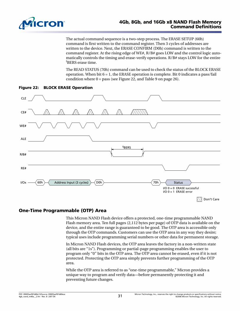
4Gb, 8Gb, and 16Gb x8 NAND Flash MemoryCommand Definitions
The actual command sequence is a two-step process. The ERASE SETUP (60h) command is first written to the command register. Then 3 cycles of addresses are written to the device. Next, the ERASE CONFIRM (D0h) command is written to the command register. At the rising edge of WE#, R/B# goes LOW and the control logic auto-matically controls the timing and erase-verify operations. R/B# stays LOW for the entire tBERS erase time.
The READ STATUS (70h) command can be used to check the status of the BLOCK ERASE operation. When bit 6 = 1, the ERASE operation is complete. Bit 0 indicates a pass/fail condition where 0 = pass (see Figure 22, and Table 9 on page 26).
Figure 22: BLOCK ERASE Operation
One-Time Programmable (OTP) Area
This Micron NAND Flash device offers a protected, one-time programmable NAND Flash memory area. Ten full pages (2,112 bytes per page) of OTP data is available on the device, and the entire range is guaranteed to be good. The OTP area is accessible only through the OTP commands. Customers can use the OTP area in any way they desire; typical uses include programming serial numbers or other data for permanent storage.
In Micron NAND Flash devices, the OTP area leaves the factory in a non-written state (all bits are “1s”). Programming or partial-page programming enables the user to program only “0” bits in the OTP area. The OTP area cannot be erased, even if it is not protected. Protecting the OTP area simply prevents further programming of the OTP area.
While the OTP area is referred to as “one-time programmable,” Micron provides a unique way to program and verify data—before permanently protecting it and preventing future changes.
RE#
CE#
ALE
CLE
I/Ox 60h Address Input (3 cycles) StatusD0h 70h
R/B#
WE#
tBERS
Don’t Care
I/O 0 = 0 ERASE successfulI/O 0 = 1 ERASE error
PDF: 09005aef81b80e13/Source: 09005aef81b80eac Micron Technology, Inc., reserves the right to change products or specifications without notice.4gb_nand_m40a__2.fm - Rev. B 2/07 EN 31 ©2006 Micron Technology, Inc. All rights reserved.
4Gb, 8Gb, and 16Gb x8 NAND Flash MemoryCommand Definitions
OTP programming and protection are accomplished in two discrete operations. First, using the OTP DATA PROGRAM (A0h-10h) command, an OTP page is programmed entirely in one operation or in up to four partial-page programming sequences. Programming can occur on other pages within the OTP area in a similar manner. Second, the OTP area is permanently protected from further programming using the OTP DATA PROTECT (A5h-10h) command. The pages within the OTP area can always be read using the OTP DATA READ (AFh-30h) command, whether or not it is protected.
To determine whether or not the device is busy during an OTP operation, either monitor R/B# or use the READ STATUS (70h) command. Use of the TWO-PLANE/MULTIPLE-DIE READ STATUS (78h) command is prohibited during and following OTP operations.
OTP DATA PROGRAM A0h-10h
The OTP DATA PROGRAM (A0h-10h) command is used to write data to the pages within the OTP area. An entire page can be programmed at one time, or a page can be partially programmed up to four times. There is no ERASE operation for the OTP pages.
The OTP DATA PROGRAM enables programming into an offset of an OTP page, using the two bytes of column address (CA[11:0]). The command is not compatible with the RANDOM DATA INPUT (85h) command. The OTP DATA PROGRAM command will not execute if the OTP area has been protected.
To use the OTP DATA PROGRAM command, issue the A0h command. Issue 5 ADDRESS cycles: the first 2 ADDRESS cycles are the column address, and for the remaining 3 cycles select a page in the range of 02h-00h-00h through 0Bh-00h-00h. Next, write from 1 to 2,112 bytes of data. After data input is complete, issue the 10h command. The internal control logic automatically executes the proper programming algorithm and controls the necessary timing for programming and verification. Program verification only detects “1s” that are not successfully written to “0s.”
R/B# goes LOW during the duration of the array programming time (tPROG). The READ STATUS (70h) command is the only command valid during the OTP DATA PROGRAM operation. Bit 5 of the status register will reflect the state of R/B#. If bit 7 is “0,” then the OTP area has been protected; otherwise, it will be a “1.”
When the device is ready, read bit 0 of the status register to determine if the operation passed or failed (see Table 9 on page 26).
It is possible to program each OTP page a maximum of four times.
PDF: 09005aef81b80e13/Source: 09005aef81b80eac Micron Technology, Inc., reserves the right to change products or specifications without notice.4gb_nand_m40a__2.fm - Rev. B 2/07 EN 32 ©2006 Micron Technology, Inc. All rights reserved.
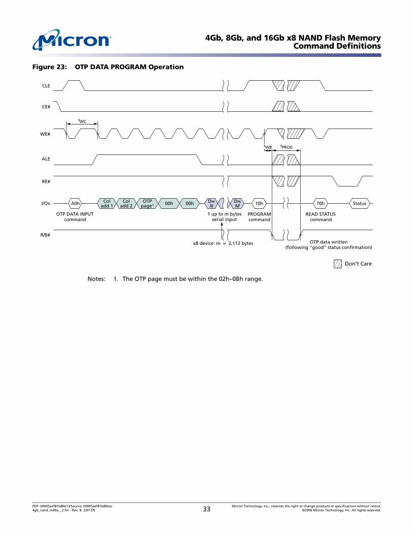
4Gb, 8Gb, and 16Gb x8 NAND Flash MemoryCommand Definitions
Figure 23: OTP DATA PROGRAM Operation
Notes: 1. The OTP page must be within the 02h–0Bh range.
WE#
CE#
ALE
CLE
RE#
R/B#
I/Ox
Don’t Care
OTP data written(following “good” status confirmation)
tWC
tPROG
OTP DATA INPUTcommand
PROGRAMcommand
READ STATUScommand
1 up to m bytesserial input
x8 device: m = 2,112 bytes
A0h Coladd 1
Coladd 2
DINN
DINM00h 00h 10h 70h StatusOTP
page1
tWB
PDF: 09005aef81b80e13/Source: 09005aef81b80eac Micron Technology, Inc., reserves the right to change products or specifications without notice.4gb_nand_m40a__2.fm - Rev. B 2/07 EN 33 ©2006 Micron Technology, Inc. All rights reserved.
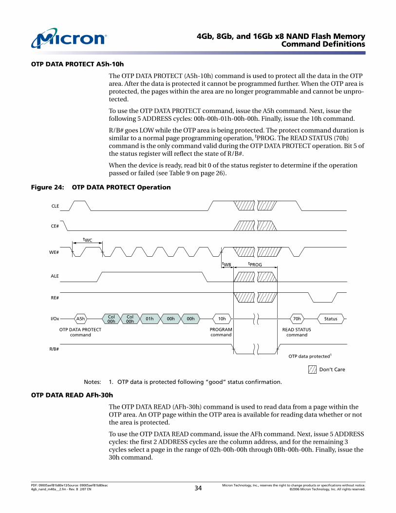
4Gb, 8Gb, and 16Gb x8 NAND Flash MemoryCommand Definitions
OTP DATA PROTECT A5h-10h
The OTP DATA PROTECT (A5h-10h) command is used to protect all the data in the OTP area. After the data is protected it cannot be programmed further. When the OTP area is protected, the pages within the area are no longer programmable and cannot be unpro-tected.
To use the OTP DATA PROTECT command, issue the A5h command. Next, issue the following 5 ADDRESS cycles: 00h-00h-01h-00h-00h. Finally, issue the 10h command.
R/B# goes LOW while the OTP area is being protected. The protect command duration is similar to a normal page programming operation, tPROG. The READ STATUS (70h) command is the only command valid during the OTP DATA PROTECT operation. Bit 5 of the status register will reflect the state of R/B#.
When the device is ready, read bit 0 of the status register to determine if the operation passed or failed (see Table 9 on page 26).
Figure 24: OTP DATA PROTECT Operation
Notes: 1. OTP data is protected following “good” status confirmation.
OTP DATA READ AFh-30h
The OTP DATA READ (AFh-30h) command is used to read data from a page within the OTP area. An OTP page within the OTP area is available for reading data whether or not the area is protected.
To use the OTP DATA READ command, issue the AFh command. Next, issue 5 ADDRESS cycles: the first 2 ADDRESS cycles are the column address, and for the remaining 3 cycles select a page in the range of 02h-00h-00h through 0Bh-00h-00h. Finally, issue the 30h command.
WE#
CE#
ALE
CLE
RE#
R/B#
I/Ox
Don’t Care
tWC
tWB tPROG
OTP DATA PROTECTcommand
OTP data protected1
PROGRAMcommand
READ STATUScommand
A5h Col00h
Col00h 10h 70h Status01h 00h 00h
PDF: 09005aef81b80e13/Source: 09005aef81b80eac Micron Technology, Inc., reserves the right to change products or specifications without notice.4gb_nand_m40a__2.fm - Rev. B 2/07 EN 34 ©2006 Micron Technology, Inc. All rights reserved.
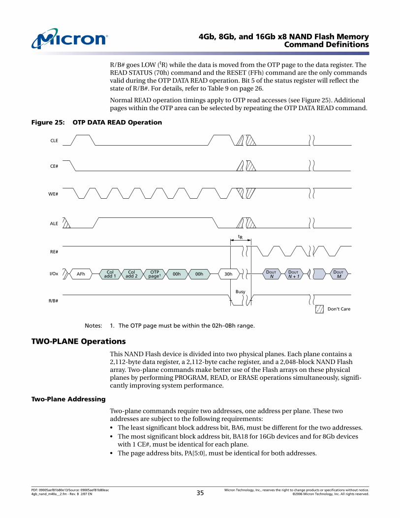
4Gb, 8Gb, and 16Gb x8 NAND Flash MemoryCommand Definitions
R/B# goes LOW (tR) while the data is moved from the OTP page to the data register. The READ STATUS (70h) command and the RESET (FFh) command are the only commands valid during the OTP DATA READ operation. Bit 5 of the status register will reflect the state of R/B#. For details, refer to Table 9 on page 26.
Normal READ operation timings apply to OTP read accesses (see Figure 25). Additional pages within the OTP area can be selected by repeating the OTP DATA READ command.
Figure 25: OTP DATA READ Operation
Notes: 1. The OTP page must be within the 02h–0Bh range.
TWO-PLANE Operations
This NAND Flash device is divided into two physical planes. Each plane contains a 2,112-byte data register, a 2,112-byte cache register, and a 2,048-block NAND Flash array. Two-plane commands make better use of the Flash arrays on these physical planes by performing PROGRAM, READ, or ERASE operations simultaneously, signifi-cantly improving system performance.
Two-Plane Addressing
Two-plane commands require two addresses, one address per plane. These two addresses are subject to the following requirements:• The least significant block address bit, BA6, must be different for the two addresses.• The most significant block address bit, BA18 for 16Gb devices and for 8Gb devices
with 1 CE#, must be identical for each plane.• The page address bits, PA[5:0], must be identical for both addresses.
WE#
CE#
ALE
CLE
RE#
R/B#
I/Ox
Busy
tR
DOUTN
DOUTN + 1
DOUTMAFh 00h 00h 30h
Don’t Care
OTPpage1
Coladd 2
Coladd 1
PDF: 09005aef81b80e13/Source: 09005aef81b80eac Micron Technology, Inc., reserves the right to change products or specifications without notice.4gb_nand_m40a__2.fm - Rev. B 2/07 EN 35 ©2006 Micron Technology, Inc. All rights reserved.
4Gb, 8Gb, and 16Gb x8 NAND Flash MemoryCommand Definitions
TWO-PLANE PAGE READ 00h-00h-30h
The TWO-PLANE PAGE READ (00h-00h-30h) operation is similar to the PAGE READ (00h-30h) operation. It transfers two pages of data from the NAND Flash array to the data registers. Each page must be from a different plane on the same die.
To enter the TWO-PLANE PAGE READ mode, write the 00h command to the command register, then write 5 ADDRESS cycles for plane 0 (BA6 = 0). Next, write the 00h command to the command register, then write 5 ADDRESS cycles for plane 1 (BA6 = 1). Finally, issue the 30h command. The first-plane and second-plane addresses must meet the two-plane addressing requirements and, in addition, they must have identical column addresses.
After the 30h command is written, page data is transferred from both planes to their respective data registers in tR. During these transfers, R/B# goes LOW. When the trans-fers are complete, R/B# goes HIGH. To read out the data from the plane 0 data register, pulse RE# repeatedly. After the data cycle from the plane 0 address completes, issue a TWO-PLANE RANDOM DATA READ (06h-E0h) command to select the plane 1 address, then repeatedly pulse RE# to read out the data from the plane 1 data register.
Alternatively, the READ STATUS (70h) command can monitor data transfers. When the transfers are complete, status register bit 6 is set to “1.” To read data from the first of the two planes, the user must first issue the TWO-PLANE RANDOM DATA READ (06h-E0h) command (see “TWO-PLANE RANDOM DATA READ 06h-E0h”) and pulse RE# repeat-edly. When the data cycle is complete, issue a TWO-PLANE RANDOM DATA READ (06h-E0h) command to select the other plane. To output the data beginning at the specified column address, pulse RE# repeatedly.
Use of the TWO-PLANE/MULTIPLE-DIE READ STATUS (78h) command is prohibited during and following a TWO-PLANE PAGE READ operation.
TWO-PLANE RANDOM DATA READ 06h-E0h
The TWO-PLANE RANDOM DATA READ (06h-E0h) command is similar to the RANDOM DATA READ (05h-E0h) command, except that it requires 5 ADDRESS cycles rather than 2. The command selects a die and plane, and a column address from which to read data after a TWO-PLANE PAGE READ (00h-00h-30h) command.
To issue a TWO-PLANE RANDOM DATA READ command, issue the 06h command, then 5 ADDRESS cycles, and follow with the E0h command. Pulse RE# repeatedly to read data from the new plane, beginning at the specified column address.
The primary purpose of the TWO-PLANE RANDOM DATA READ command is to select a new die and plane, and a column address within that die and plane. If a new die and plane do not need to be selected, then it is possible to use the RANDOM DATA READ (05h-E0h) command instead (see “RANDOM DATA READ 05h-E0h” on page 22).
PDF: 09005aef81b80e13/Source: 09005aef81b80eac Micron Technology, Inc., reserves the right to change products or specifications without notice.4gb_nand_m40a__2.fm - Rev. B 2/07 EN 36 ©2006 Micron Technology, Inc. All rights reserved.
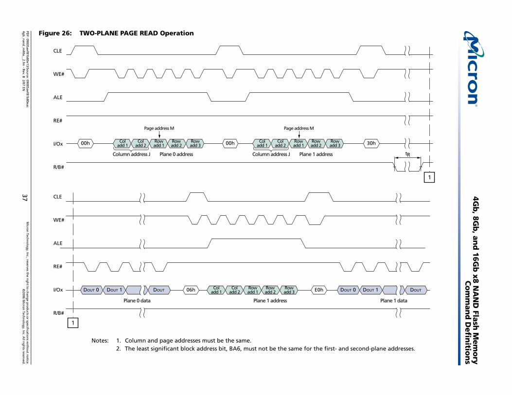
PDF: 09005aef81b
4gb
_nan
d_m
40a__2.fm-
Rev. B
2/07 EN37
©2006 M
icron
Techn
olo
gy, In
c. All rig
hts reserved
.
4Gb
, 8Gb
, and
16Gb
x8 NA
ND
Flash M
emo
ryC
om
man
d D
efinitio
ns
Figure 26: TWO-PLANE PAGE READ Operation
plane addresses.
CLE
h
T 1 DOUT
tR
Plane 1 data
1
80e13/Sou
rce: 09005aef81b80eac
Micro
n Tech
no
log
y, Inc., reserves th
e righ
t to ch
ang
e pro
du
cts or sp
ecification
s with
ou
t no
tice.
Notes: 1. Column and page addresses must be the same.2. The least significant block address bit, BA6, must not be the same for the first- and second-
WE#
ALE
RE#
I/Ox
R/B#
CLE
WE#
ALE
RE#
I/Ox
R/B#
00h Coladd 1
Coladd 2
Rowadd 1
Rowadd 2
Rowadd 3
Coladd 1
Coladd 2
Rowadd 1
Rowadd 2
Rowadd 3
Coladd 1
Coladd 2
Rowadd 1
Rowadd 2
Rowadd 3
00h 30
DOUT 0 DOUT 1 DOUT 06h E0h DOUT 0 DOU
Plane 0 addressColumn address J Plane 1 address
Plane 1 addressPlane 0 data
Page address M Page address M
1
Column address J
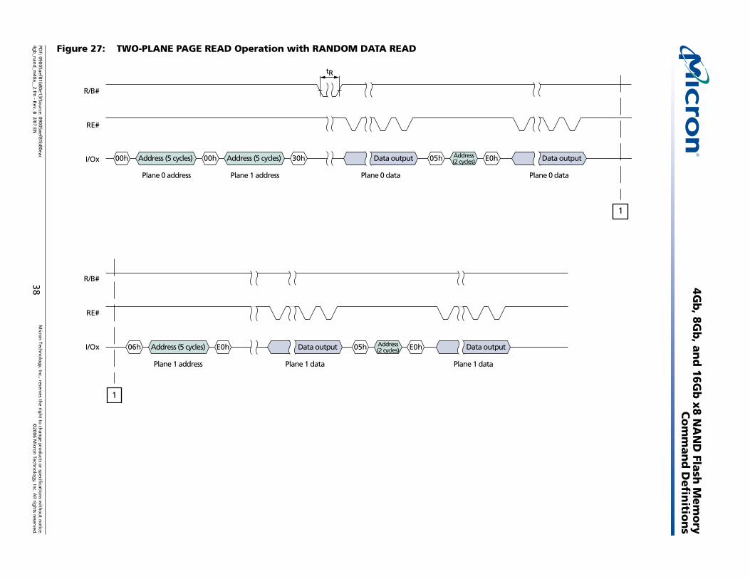
PDF: 09005aef81b
4gb
_nan
d_m
40a__2.fm-
Rev. B
2/07 EN38
©2006 M
icron
Techn
olo
gy, In
c. All rig
hts reserved
.
4Gb
, 8Gb
, and
16Gb
x8 NA
ND
Flash M
emo
ryC
om
man
d D
efinitio
ns
Figure 27: TWO-PLANE PAGE READ Operation with RANDOM DATA READ
tR
e 0 data
ata output
1
80e13/Sou
rce: 09005aef81b80eac
Micro
n Tech
no
log
y, Inc., reserves th
e righ
t to ch
ang
e pro
du
cts or sp
ecification
s with
ou
t no
tice.
R/B#
RE#
I/Ox
R/B#
RE#
I/Ox
00h 00hAddress (5 cycles) 05h E0h30h
Plane 0 address Plane 0 data Plan
Address (5 cycles) Address(2 cycles)Data output D
Plane 1 address
06h 05h E0hE0h
Plane 1 data Plane 1 data
Address (5 cycles) Address(2 cycles)Data output Data output
Plane 1 address
1
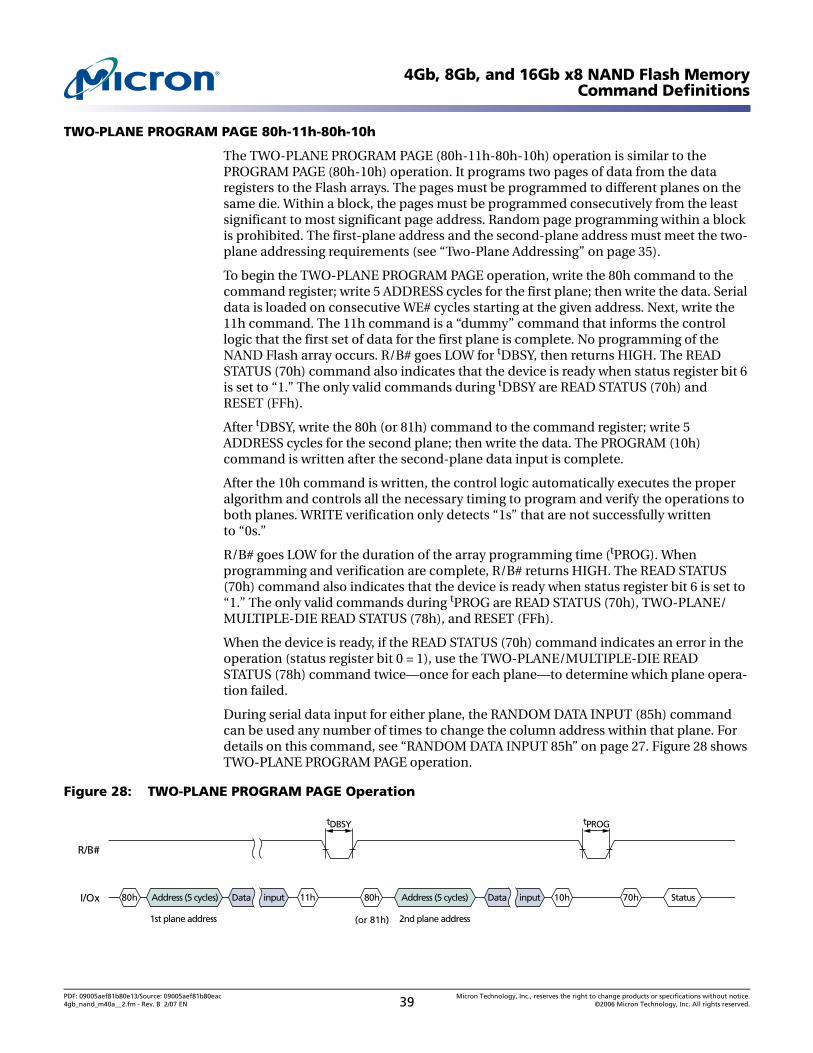
4Gb, 8Gb, and 16Gb x8 NAND Flash MemoryCommand Definitions
TWO-PLANE PROGRAM PAGE 80h-11h-80h-10h
The TWO-PLANE PROGRAM PAGE (80h-11h-80h-10h) operation is similar to the PROGRAM PAGE (80h-10h) operation. It programs two pages of data from the data registers to the Flash arrays. The pages must be programmed to different planes on the same die. Within a block, the pages must be programmed consecutively from the least significant to most significant page address. Random page programming within a block is prohibited. The first-plane address and the second-plane address must meet the two-plane addressing requirements (see “Two-Plane Addressing” on page 35).
To begin the TWO-PLANE PROGRAM PAGE operation, write the 80h command to the command register; write 5 ADDRESS cycles for the first plane; then write the data. Serial data is loaded on consecutive WE# cycles starting at the given address. Next, write the 11h command. The 11h command is a “dummy” command that informs the control logic that the first set of data for the first plane is complete. No programming of the NAND Flash array occurs. R/B# goes LOW for tDBSY, then returns HIGH. The READ STATUS (70h) command also indicates that the device is ready when status register bit 6 is set to “1.” The only valid commands during tDBSY are READ STATUS (70h) and RESET (FFh).
After tDBSY, write the 80h (or 81h) command to the command register; write 5 ADDRESS cycles for the second plane; then write the data. The PROGRAM (10h) command is written after the second-plane data input is complete.
After the 10h command is written, the control logic automatically executes the proper algorithm and controls all the necessary timing to program and verify the operations to both planes. WRITE verification only detects “1s” that are not successfully written to “0s.”
R/B# goes LOW for the duration of the array programming time (tPROG). When programming and verification are complete, R/B# returns HIGH. The READ STATUS (70h) command also indicates that the device is ready when status register bit 6 is set to “1.” The only valid commands during tPROG are READ STATUS (70h), TWO-PLANE/MULTIPLE-DIE READ STATUS (78h), and RESET (FFh).
When the device is ready, if the READ STATUS (70h) command indicates an error in the operation (status register bit 0 = 1), use the TWO-PLANE/MULTIPLE-DIE READ STATUS (78h) command twice—once for each plane—to determine which plane opera-tion failed.
During serial data input for either plane, the RANDOM DATA INPUT (85h) command can be used any number of times to change the column address within that plane. For details on this command, see “RANDOM DATA INPUT 85h” on page 27. Figure 28 shows TWO-PLANE PROGRAM PAGE operation.
Figure 28: TWO-PLANE PROGRAM PAGE Operation
R/B#
I/Ox 80h Address (5 cycles) 70h10h11h 80h
(or 81h)
tDBSY tPROG
1st plane address
Address (5 cycles)Data input Data input Status
2nd plane address
PDF: 09005aef81b80e13/Source: 09005aef81b80eac Micron Technology, Inc., reserves the right to change products or specifications without notice.4gb_nand_m40a__2.fm - Rev. B 2/07 EN 39 ©2006 Micron Technology, Inc. All rights reserved.
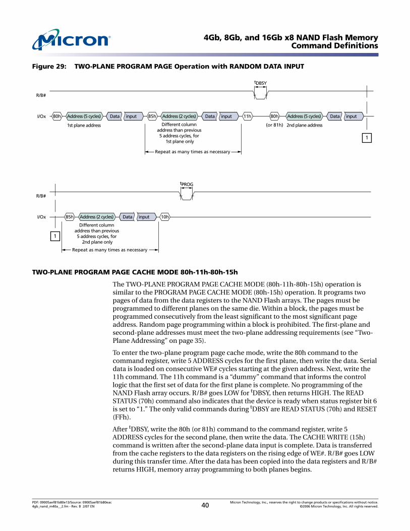
4Gb, 8Gb, and 16Gb x8 NAND Flash MemoryCommand Definitions
Figure 29: TWO-PLANE PROGRAM PAGE Operation with RANDOM DATA INPUT
TWO-PLANE PROGRAM PAGE CACHE MODE 80h-11h-80h-15h
The TWO-PLANE PROGRAM PAGE CACHE MODE (80h-11h-80h-15h) operation is similar to the PROGRAM PAGE CACHE MODE (80h-15h) operation. It programs two pages of data from the data registers to the NAND Flash arrays. The pages must be programmed to different planes on the same die. Within a block, the pages must be programmed consecutively from the least significant to the most significant page address. Random page programming within a block is prohibited. The first-plane and second-plane addresses must meet the two-plane addressing requirements (see “Two-Plane Addressing” on page 35).
To enter the two-plane program page cache mode, write the 80h command to the command register, write 5 ADDRESS cycles for the first plane, then write the data. Serial data is loaded on consecutive WE# cycles starting at the given address. Next, write the 11h command. The 11h command is a “dummy” command that informs the control logic that the first set of data for the first plane is complete. No programming of the NAND Flash array occurs. R/B# goes LOW for tDBSY, then returns HIGH. The READ STATUS (70h) command also indicates that the device is ready when status register bit 6 is set to “1.” The only valid commands during tDBSY are READ STATUS (70h) and RESET (FFh).
After tDBSY, write the 80h (or 81h) command to the command register, write 5 ADDRESS cycles for the second plane, then write the data. The CACHE WRITE (15h) command is written after the second-plane data input is complete. Data is transferred from the cache registers to the data registers on the rising edge of WE#. R/B# goes LOW during this transfer time. After the data has been copied into the data registers and R/B# returns HIGH, memory array programming to both planes begins.
R/B#
I/Ox
R/B#
I/Ox
80h Address (5 cycles) 11h 80h
(or 81h)
85h
tDBSY
tPROG
1st plane address
Address (2 cycles)Data input Address (5 cycles)
2nd plane address
Data inputData input
85h 10hAddress (2 cycles)
1
1
Data input
Different column address than previous 5 address cycles, for
1st plane only
Different column address than previous 5 address cycles, for
2nd plane only
Repeat as many times as necessary
Repeat as many times as necessary
PDF: 09005aef81b80e13/Source: 09005aef81b80eac Micron Technology, Inc., reserves the right to change products or specifications without notice.4gb_nand_m40a__2.fm - Rev. B 2/07 EN 40 ©2006 Micron Technology, Inc. All rights reserved.
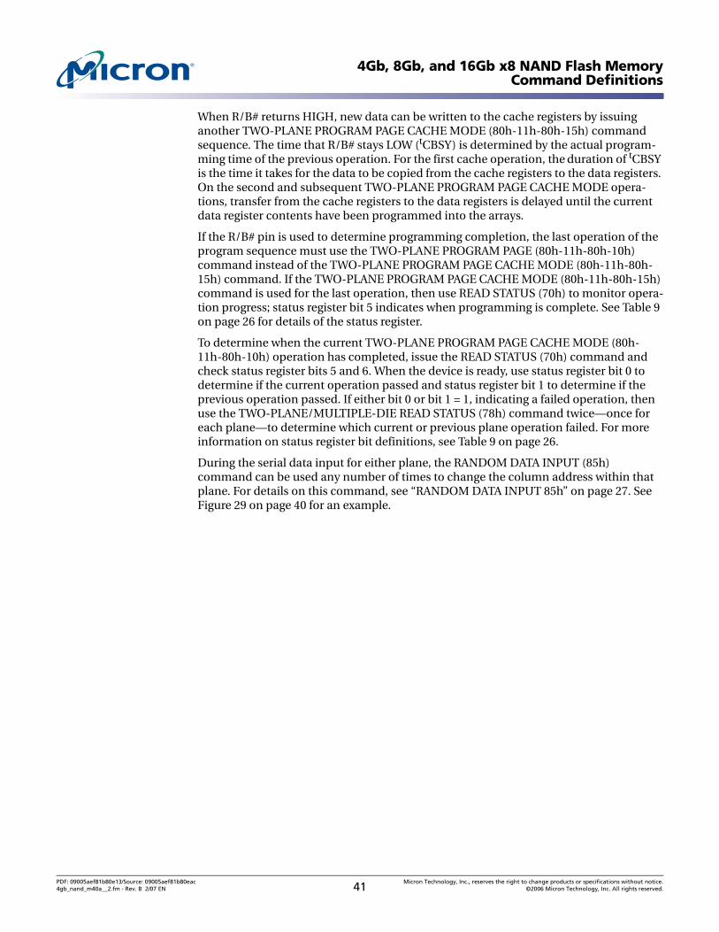
4Gb, 8Gb, and 16Gb x8 NAND Flash MemoryCommand Definitions
When R/B# returns HIGH, new data can be written to the cache registers by issuing another TWO-PLANE PROGRAM PAGE CACHE MODE (80h-11h-80h-15h) command sequence. The time that R/B# stays LOW (tCBSY) is determined by the actual program-ming time of the previous operation. For the first cache operation, the duration of tCBSY is the time it takes for the data to be copied from the cache registers to the data registers. On the second and subsequent TWO-PLANE PROGRAM PAGE CACHE MODE opera-tions, transfer from the cache registers to the data registers is delayed until the current data register contents have been programmed into the arrays.
If the R/B# pin is used to determine programming completion, the last operation of the program sequence must use the TWO-PLANE PROGRAM PAGE (80h-11h-80h-10h) command instead of the TWO-PLANE PROGRAM PAGE CACHE MODE (80h-11h-80h-15h) command. If the TWO-PLANE PROGRAM PAGE CACHE MODE (80h-11h-80h-15h) command is used for the last operation, then use READ STATUS (70h) to monitor opera-tion progress; status register bit 5 indicates when programming is complete. See Table 9 on page 26 for details of the status register.
To determine when the current TWO-PLANE PROGRAM PAGE CACHE MODE (80h-11h-80h-10h) operation has completed, issue the READ STATUS (70h) command and check status register bits 5 and 6. When the device is ready, use status register bit 0 to determine if the current operation passed and status register bit 1 to determine if the previous operation passed. If either bit 0 or bit 1 = 1, indicating a failed operation, then use the TWO-PLANE/MULTIPLE-DIE READ STATUS (78h) command twice—once for each plane—to determine which current or previous plane operation failed. For more information on status register bit definitions, see Table 9 on page 26.
During the serial data input for either plane, the RANDOM DATA INPUT (85h) command can be used any number of times to change the column address within that plane. For details on this command, see “RANDOM DATA INPUT 85h” on page 27. See Figure 29 on page 40 for an example.
PDF: 09005aef81b80e13/Source: 09005aef81b80eac Micron Technology, Inc., reserves the right to change products or specifications without notice.4gb_nand_m40a__2.fm - Rev. B 2/07 EN 41 ©2006 Micron Technology, Inc. All rights reserved.
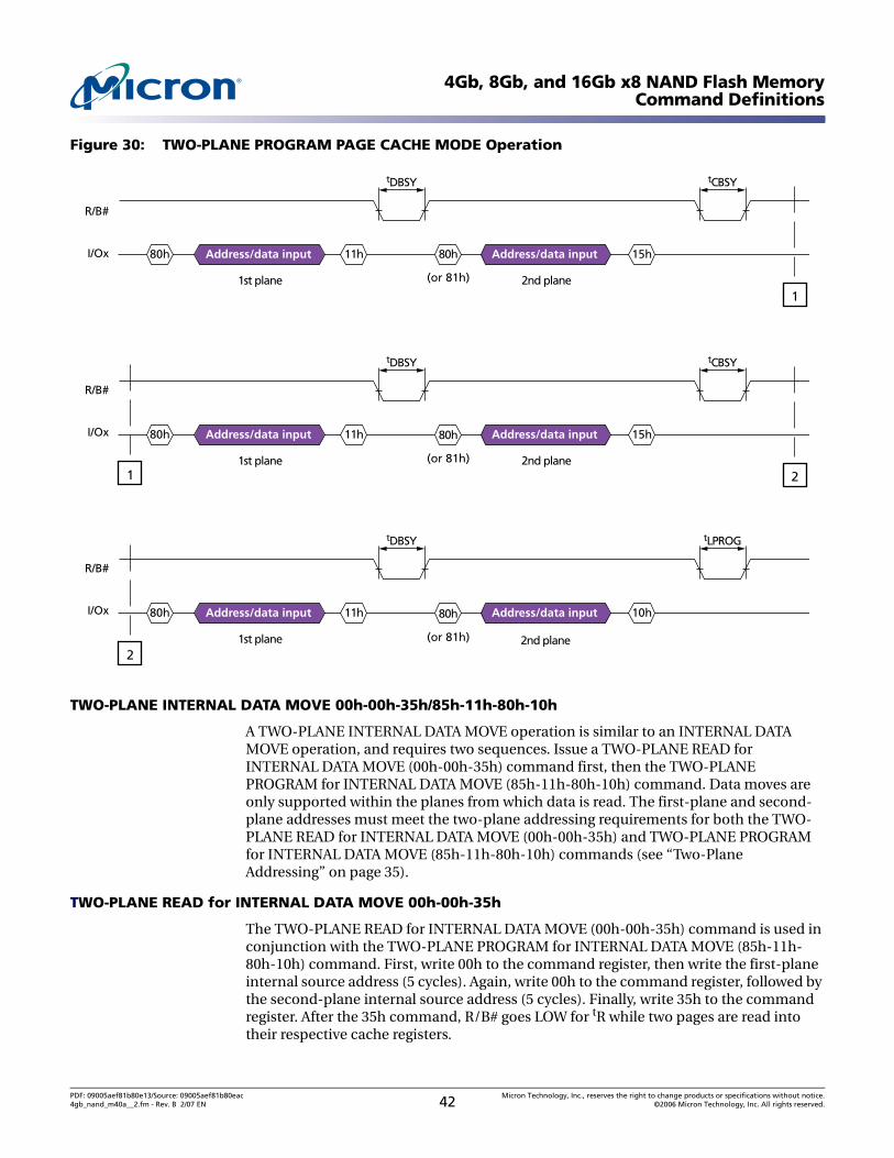
4Gb, 8Gb, and 16Gb x8 NAND Flash MemoryCommand Definitions
Figure 30: TWO-PLANE PROGRAM PAGE CACHE MODE Operation
TWO-PLANE INTERNAL DATA MOVE 00h-00h-35h/85h-11h-80h-10h
A TWO-PLANE INTERNAL DATA MOVE operation is similar to an INTERNAL DATA MOVE operation, and requires two sequences. Issue a TWO-PLANE READ for INTERNAL DATA MOVE (00h-00h-35h) command first, then the TWO-PLANE PROGRAM for INTERNAL DATA MOVE (85h-11h-80h-10h) command. Data moves are only supported within the planes from which data is read. The first-plane and second-plane addresses must meet the two-plane addressing requirements for both the TWO-PLANE READ for INTERNAL DATA MOVE (00h-00h-35h) and TWO-PLANE PROGRAM for INTERNAL DATA MOVE (85h-11h-80h-10h) commands (see “Two-Plane Addressing” on page 35).
TWO-PLANE READ for INTERNAL DATA MOVE 00h-00h-35h
The TWO-PLANE READ for INTERNAL DATA MOVE (00h-00h-35h) command is used in conjunction with the TWO-PLANE PROGRAM for INTERNAL DATA MOVE (85h-11h-80h-10h) command. First, write 00h to the command register, then write the first-plane internal source address (5 cycles). Again, write 00h to the command register, followed by the second-plane internal source address (5 cycles). Finally, write 35h to the command register. After the 35h command, R/B# goes LOW for tR while two pages are read into their respective cache registers.
R/B#
I/Ox 80h Address/data input 11h 80h
(or 81h)
15h
tDBSY tCBSY
1st plane 2nd plane
Address/data input
1
1
2
R/B#
I/Ox 80h Address/data input 11h 15h
tDBSY tCBSY
1st plane 2nd plane
Address/data input
2
R/B#
I/Ox 80h Address/data input 11h 10h
tDBSY tLPROG
1st plane 2nd plane
Address/data input
80h
(or 81h)
80h
(or 81h)
PDF: 09005aef81b80e13/Source: 09005aef81b80eac Micron Technology, Inc., reserves the right to change products or specifications without notice.4gb_nand_m40a__2.fm - Rev. B 2/07 EN 42 ©2006 Micron Technology, Inc. All rights reserved.
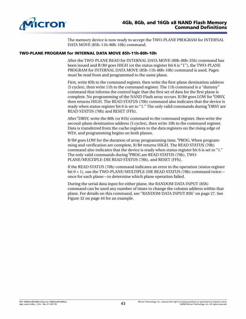
4Gb, 8Gb, and 16Gb x8 NAND Flash MemoryCommand Definitions
The memory device is now ready to accept the TWO-PLANE PROGRAM for INTERNAL DATA MOVE (85h-11h-80h-10h) command.
TWO-PLANE PROGRAM for INTERNAL DATA MOVE 85h-11h-80h-10h
After the TWO-PLANE READ for INTERNAL DATA MOVE (00h-00h-35h) command has been issued and R/B# goes HIGH (or the status register bit 6 is “1”), the TWO-PLANE PROGRAM for INTERNAL DATA MOVE (85h-11h-80h-10h) command is used. Pages must be read from and programmed to the same plane.
First, write 85h to the command register, then write the first-plane destination address (5 cycles), then write 11h to the command register. The 11h command is a “dummy” command that informs the control logic that the first set of data for the first plane is complete. No programming of the NAND Flash array occurs. R/B# goes LOW for tDBSY, then returns HIGH. The READ STATUS (70h) command also indicates that the device is ready when status register bit 6 is set to “1.” The only valid commands during tDBSY are READ STATUS (70h) and RESET (FFh).
After tDBSY, write the 80h (or 81h) command to the command register, then write the second-plane destination address (5 cycles), then write 10h to the command register. Data is transferred from the cache registers to the data registers on the rising edge of WE#, and programming begins on both planes.
R/B# goes LOW for the duration of array programming time, tPROG. When program-ming and verification are complete, R/B# returns HIGH. The READ STATUS (70h) command also indicates that the device is ready when status register bit 6 is set to “1.” The only valid commands during tPROG are READ STATUS (70h), TWO-PLANE/MULTIPLE-DIE READ STATUS (78h), and RESET (FFh).
If the READ STATUS (70h) command indicates an error in the operation (status register bit 0 = 1), use the TWO-PLANE/MULTIPLE-DIE READ STATUS (78h) command twice—once for each plane—to determine which plane operation failed.
During the serial data input for either plane, the RANDOM DATA INPUT (85h) command can be used any number of times to change the column address within that plane. For details on this command, see “RANDOM DATA INPUT 85h” on page 27. See Figure 32 on page 44 for an example.
PDF: 09005aef81b80e13/Source: 09005aef81b80eac Micron Technology, Inc., reserves the right to change products or specifications without notice.4gb_nand_m40a__2.fm - Rev. B 2/07 EN 43 ©2006 Micron Technology, Inc. All rights reserved.
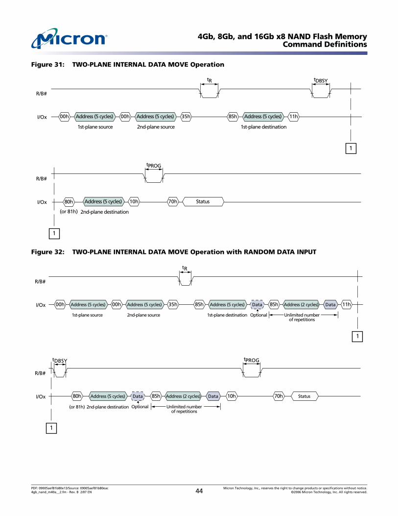
4Gb, 8Gb, and 16Gb x8 NAND Flash MemoryCommand Definitions
Figure 31: TWO-PLANE INTERNAL DATA MOVE Operation
Figure 32: TWO-PLANE INTERNAL DATA MOVE Operation with RANDOM DATA INPUT
R/B#
I/Ox 00h 00hAddress (5 cycles) 35h
tR tDBSY
1st-plane source
85h 11hAddress (5 cycles)
1st-plane destination
Address (5 cycles)
2nd-plane source
1
R/B#
I/Ox 80h
(or 81h)
10hAddress (5 cycles)
tPROG
2nd-plane destination
70h Status
1
R/B#
I/Ox 00h 00hAddress (5 cycles) 35h
tR
tDBSY
1st-plane source 1st-plane destination
2nd-plane destination
85h Data DataAddress (5 cycles)
Optional
85h 11hAddress (2 cycles)Address (5 cycles)
2nd-plane source
1
R/B#
I/Ox
tPROG
80h
(or 81h)
Data DataAddress (5 cycles)
Optional
85h 10h 70h StatusAddress (2 cycles)
1
Unlimited numberof repetitions
Unlimited numberof repetitions
PDF: 09005aef81b80e13/Source: 09005aef81b80eac Micron Technology, Inc., reserves the right to change products or specifications without notice.4gb_nand_m40a__2.fm - Rev. B 2/07 EN 44 ©2006 Micron Technology, Inc. All rights reserved.
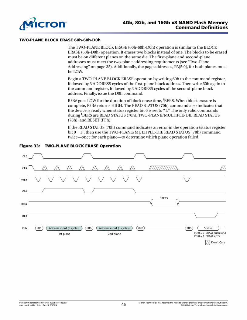
4Gb, 8Gb, and 16Gb x8 NAND Flash MemoryCommand Definitions
TWO-PLANE BLOCK ERASE 60h-60h-D0h
The TWO-PLANE BLOCK ERASE (60h-60h-D0h) operation is similar to the BLOCK ERASE (60h-D0h) operation. It erases two blocks instead of one. The blocks to be erased must be on different planes on the same die. The first-plane and second-plane addresses must meet the two-plane addressing requirements (see “Two-Plane Addressing” on page 35). Additionally, the page addresses, PA[5:0], for both planes must be LOW.
Begin a TWO-PLANE BLOCK ERASE operation by writing 60h to the command register, followed by 3 ADDRESS cycles of the first-plane block address. Then write 60h again to the command register, followed by 3 ADDRESS cycles of the second-plane block address. Finally, issue the D0h command.
R/B# goes LOW for the duration of block erase time, tBERS. When block erasure is complete, R/B# returns HIGH. The READ STATUS (70h) command also indicates that the device is ready when status register bit 6 is set to “1.” The only valid commands during tBERS are READ STATUS (70h), TWO-PLANE/MULTIPLE-DIE READ STATUS (78h), and RESET (FFh).
If the READ STATUS (70h) command indicates an error in the operation (status register bit 0 = 1), then use the TWO-PLANE/MULTIPLE-DIE READ STATUS (78h) command twice—once for each plane—to determine which plane operation failed.
Figure 33: TWO-PLANE BLOCK ERASE Operation
RE#
CE#
ALE
CLE
I/Ox 60h Address input (3 cycles) StatusD0h 70h
R/B#
WE#
tBERS
Don’t Care
60h Address input (3 cycles)
I/O 0 = 0 ERASE successfulI/O 0 = 1 ERASE error
1st plane 2nd plane
PDF: 09005aef81b80e13/Source: 09005aef81b80eac Micron Technology, Inc., reserves the right to change products or specifications without notice.4gb_nand_m40a__2.fm - Rev. B 2/07 EN 45 ©2006 Micron Technology, Inc. All rights reserved.
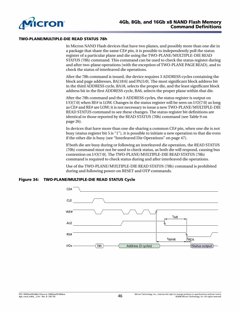
4Gb, 8Gb, and 16Gb x8 NAND Flash MemoryCommand Definitions
TWO-PLANE/MULTIPLE-DIE READ STATUS 78h
In Micron NAND Flash devices that have two planes, and possibly more than one die in a package that share the same CE# pin, it is possible to independently poll the status register of a particular plane and die using the TWO-PLANE/MULTIPLE-DIE READ STATUS (78h) command. This command can be used to check the status register during and after two-plane operations (with the exception of TWO-PLANE PAGE READ), and to check the status of interleaved die operations.
After the 78h command is issued, the device requires 3 ADDRESS cycles containing the block and page addresses, BA[18:6] and PA[5:0]. The most significant block address bit in the third ADDRESS cycle, BA18, selects the proper die, and the least significant block address bit in the first ADDRESS cycle, BA6, selects the proper plane within that die.
After the 78h command and the 3 ADDRESS cycles, the status register is output on I/O[7:0] when RE# is LOW. Changes in the status register will be seen on I/O[7:0] as long as CE# and RE# are LOW; it is not necessary to issue a new TWO-PLANE/MULTIPLE-DIE READ STATUS command to see these changes. The status register bit definitions are identical to those reported by the READ STATUS (70h) command (see Table 9 on page 26).
In devices that have more than one die sharing a common CE# pin, when one die is not busy (status register bit 5 is “1”), it is possible to initiate a new operation to that die even if the other die is busy (see “Interleaved Die Operations” on page 47).
If both die are busy during or following an interleaved die operation, the READ STATUS (70h) command must not be used to check status, as both die will respond, causing bus contention on I/O[7:0]. The TWO-PLANE/MULTIPLE-DIE READ STATUS (78h) command is required to check status during and after interleaved die operations.
Use of the TWO-PLANE/MULTIPLE-DIE READ STATUS (78h) command is prohibited during and following power-on RESET and OTP commands.
Figure 34: TWO-PLANE/MULTIPLE-DIE READ STATUS Cycle
78h Address (3 cycles) Status output
tWHR
tAR
tREA
CE#
CLE
WE#
ALE
RE#
I/Ox
PDF: 09005aef81b80e13/Source: 09005aef81b80eac Micron Technology, Inc., reserves the right to change products or specifications without notice.4gb_nand_m40a__2.fm - Rev. B 2/07 EN 46 ©2006 Micron Technology, Inc. All rights reserved.
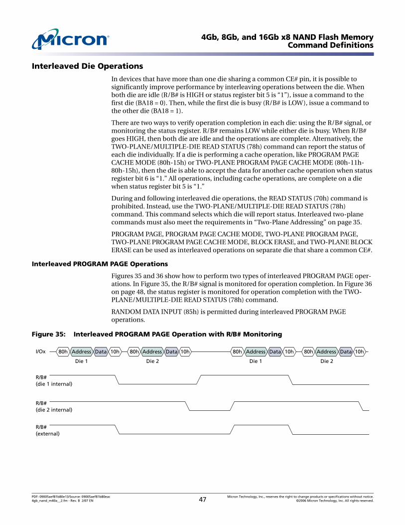
4Gb, 8Gb, and 16Gb x8 NAND Flash MemoryCommand Definitions
Interleaved Die Operations
In devices that have more than one die sharing a common CE# pin, it is possible to significantly improve performance by interleaving operations between the die. When both die are idle (R/B# is HIGH or status register bit 5 is “1”), issue a command to the first die (BA18 = 0). Then, while the first die is busy (R/B# is LOW), issue a command to the other die (BA18 = 1).
There are two ways to verify operation completion in each die: using the R/B# signal, or monitoring the status register. R/B# remains LOW while either die is busy. When R/B# goes HIGH, then both die are idle and the operations are complete. Alternatively, the TWO-PLANE/MULTIPLE-DIE READ STATUS (78h) command can report the status of each die individually. If a die is performing a cache operation, like PROGRAM PAGE CACHE MODE (80h-15h) or TWO-PLANE PROGRAM PAGE CACHE MODE (80h-11h-80h-15h), then the die is able to accept the data for another cache operation when status register bit 6 is “1.” All operations, including cache operations, are complete on a die when status register bit 5 is “1.”
During and following interleaved die operations, the READ STATUS (70h) command is prohibited. Instead, use the TWO-PLANE/MULTIPLE-DIE READ STATUS (78h) command. This command selects which die will report status. Interleaved two-plane commands must also meet the requirements in “Two-Plane Addressing” on page 35.
PROGRAM PAGE, PROGRAM PAGE CACHE MODE, TWO-PLANE PROGRAM PAGE, TWO-PLANE PROGRAM PAGE CACHE MODE, BLOCK ERASE, and TWO-PLANE BLOCK ERASE can be used as interleaved operations on separate die that share a common CE#.
Interleaved PROGRAM PAGE Operations
Figures 35 and 36 show how to perform two types of interleaved PROGRAM PAGE oper-ations. In Figure 35, the R/B# signal is monitored for operation completion. In Figure 36 on page 48, the status register is monitored for operation completion with the TWO-PLANE/MULTIPLE-DIE READ STATUS (78h) command.
RANDOM DATA INPUT (85h) is permitted during interleaved PROGRAM PAGE operations.
Figure 35: Interleaved PROGRAM PAGE Operation with R/B# Monitoring
DataAddress80h 10h DataAddress80h 10h
Die 1 Die 2
DataAddress80h 10h DataAddress80h 10h
Die 1 Die 2
I/Ox
R/B#(die 1 internal)
R/B#(die 2 internal)
R/B#(external)
PDF: 09005aef81b80e13/Source: 09005aef81b80eac Micron Technology, Inc., reserves the right to change products or specifications without notice.4gb_nand_m40a__2.fm - Rev. B 2/07 EN 47 ©2006 Micron Technology, Inc. All rights reserved.
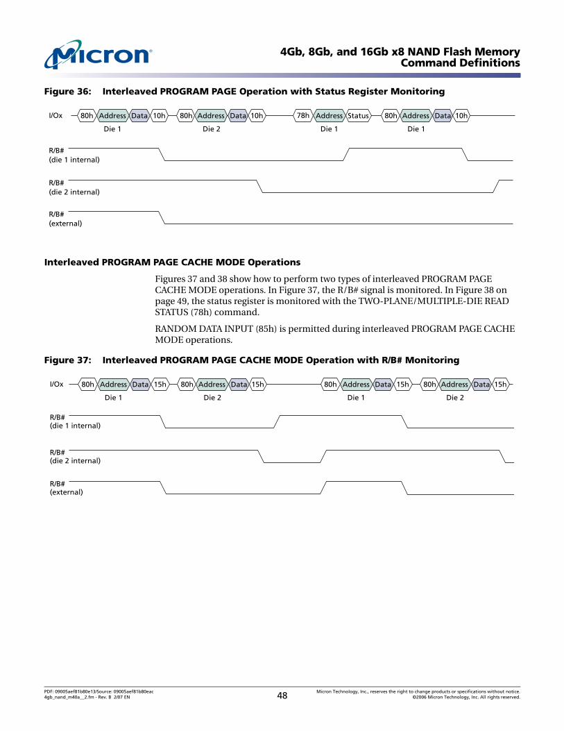
4Gb, 8Gb, and 16Gb x8 NAND Flash MemoryCommand Definitions
Figure 36: Interleaved PROGRAM PAGE Operation with Status Register Monitoring
Interleaved PROGRAM PAGE CACHE MODE Operations
Figures 37 and 38 show how to perform two types of interleaved PROGRAM PAGE CACHE MODE operations. In Figure 37, the R/B# signal is monitored. In Figure 38 on page 49, the status register is monitored with the TWO-PLANE/MULTIPLE-DIE READ STATUS (78h) command.
RANDOM DATA INPUT (85h) is permitted during interleaved PROGRAM PAGE CACHE MODE operations.
Figure 37: Interleaved PROGRAM PAGE CACHE MODE Operation with R/B# Monitoring
DataAddress80h 10h DataAddress80h 10h
Die 1 Die 2
StatusAddress DataAddress80h 10h
Die 1 Die 1
I/Ox
R/B#(die 1 internal)
R/B#(die 2 internal)
R/B#(external)
78h
DataAddress80h 15h DataAddress80h 15h
Die 1 Die 2
DataAddress80h 15h DataAddress80h 15h
Die 1 Die 2
I/Ox
R/B#(die 1 internal)
R/B#(die 2 internal)
R/B#(external)
PDF: 09005aef81b80e13/Source: 09005aef81b80eac Micron Technology, Inc., reserves the right to change products or specifications without notice.4gb_nand_m40a__2.fm - Rev. B 2/07 EN 48 ©2006 Micron Technology, Inc. All rights reserved.
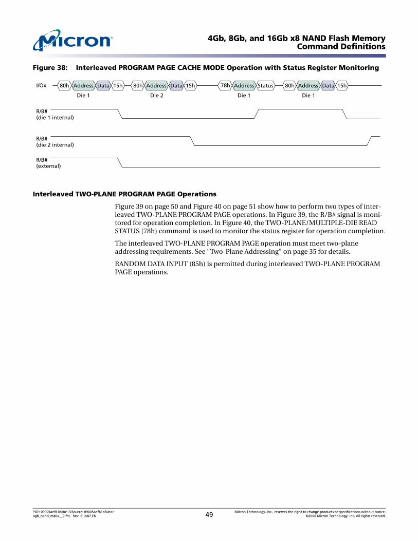
4Gb, 8Gb, and 16Gb x8 NAND Flash MemoryCommand Definitions
Figure 38: Interleaved PROGRAM PAGE CACHE MODE Operation with Status Register Monitoring
Interleaved TWO-PLANE PROGRAM PAGE Operations
Figure 39 on page 50 and Figure 40 on page 51 show how to perform two types of inter-leaved TWO-PLANE PROGRAM PAGE operations. In Figure 39, the R/B# signal is moni-tored for operation completion. In Figure 40, the TWO-PLANE/MULTIPLE-DIE READ STATUS (78h) command is used to monitor the status register for operation completion.
The interleaved TWO-PLANE PROGRAM PAGE operation must meet two-plane addressing requirements. See “Two-Plane Addressing” on page 35 for details.
RANDOM DATA INPUT (85h) is permitted during interleaved TWO-PLANE PROGRAM PAGE operations.
DataAddress80h 15h DataAddress80h 15h
Die 1 Die 2
StatusAddress DataAddress80h 15h
Die 1 Die 1
I/Ox
R/B#(die 1 internal)
R/B#(die 2 internal)
R/B#(external)
78h
PDF: 09005aef81b80e13/Source: 09005aef81b80eac Micron Technology, Inc., reserves the right to change products or specifications without notice.4gb_nand_m40a__2.fm - Rev. B 2/07 EN 49 ©2006 Micron Technology, Inc. All rights reserved.
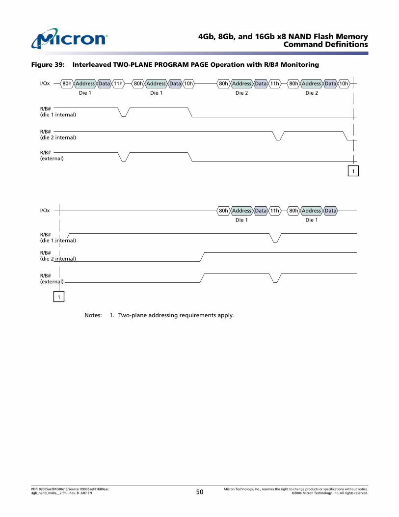
4Gb, 8Gb, and 16Gb x8 NAND Flash MemoryCommand Definitions
Figure 39: Interleaved TWO-PLANE PROGRAM PAGE Operation with R/B# Monitoring
Notes: 1. Two-plane addressing requirements apply.
1
DataAddress80h 11h DataAddress80h 10h
Die 1 Die 1
DataAddress80h 11h DataAddress80h 10h
Die 2 Die 2
I/Ox
R/B#(die 1 internal)
R/B#(die 2 internal)
R/B#(external)
1
DataAddress80h 11h DataAddress80h
Die 1 Die 1
I/Ox
R/B#(die 1 internal)
R/B#(die 2 internal)
R/B#(external)
PDF: 09005aef81b80e13/Source: 09005aef81b80eac Micron Technology, Inc., reserves the right to change products or specifications without notice.4gb_nand_m40a__2.fm - Rev. B 2/07 EN 50 ©2006 Micron Technology, Inc. All rights reserved.
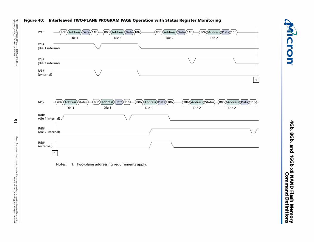
PDF: 09005aef81b
4gb
_nan
d_m
40a__2.fm-
Rev. B
2/07 EN51
©2006 M
icron
Techn
olo
gy, In
c. All rig
hts reserved
.
4Gb
, 8Gb
, and
16Gb
x8 NA
ND
Flash M
emo
ryC
om
man
d D
efinitio
ns
Figure 40: Interleaved TWO-PLANE PROGRAM PAGE Operation with Status Register Monitoring
1
DataAddress80h 11h DataAddress80h 10h DataAddress80h 11h DataAddress80h 10h
Dataddress 11h
Die 2
I/Ox
80e13/Sou
rce: 09005aef81b80eac
Micro
n Tech
no
log
y, Inc., reserves th
e righ
t to ch
ang
e pro
du
cts or sp
ecification
s with
ou
t no
tice.
Notes: 1. Two-plane addressing requirements apply.
Die 1 Die 1 Die 2 Die 2
Address DataAddress80h 11h
Die 1 Die 1
DataAddress80h 10h Address
Die 1
A80h
Die 2
R/B#(die 1 internal)
R/B#(die 2 internal)
R/B#(external)
Status Status78h78h
1
I/Ox
R/B#(die 1 internal)
R/B#(die 2 internal)
R/B#(external)
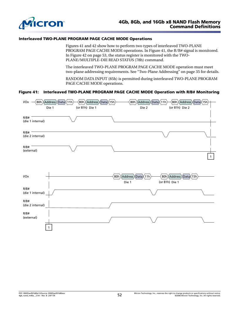
4Gb, 8Gb, and 16Gb x8 NAND Flash MemoryCommand Definitions
Interleaved TWO-PLANE PROGRAM PAGE CACHE MODE Operations
Figures 41 and 42 show how to perform two types of interleaved TWO-PLANE PROGRAM PAGE CACHE MODE operations. In Figure 41, the R/B# signal is monitored. In Figure 42 on page 53, the status register is monitored with the TWO-PLANE/MULTIPLE-DIE READ STATUS (78h) command.
The interleaved TWO-PLANE PROGRAM PAGE CACHE MODE operation must meet two-plane addressing requirements. See “Two-Plane Addressing” on page 35 for details.
RANDOM DATA INPUT (85h) is permitted during interleaved TWO-PLANE PROGRAM PAGE CACHE MODE operations.
Figure 41: Interleaved TWO-PLANE PROGRAM PAGE CACHE MODE Operation with R/B# Monitoring
1
DataAddress80h 11h DataAddress 15h
Die 1 Die 1
DataAddress80h 11h DataAddress80h
(or 81h)
80h
(or 81h)
15h
Die 2 Die 2
I/Ox
R/B#(die 1 internal)
R/B#(die 2 internal)
R/B#(external)
1
DataAddress80h 11h DataAddress80h
(or 81h)Die 1 Die 1
I/Ox
R/B#(die 1 internal)
R/B#(die 2 internal)
R/B#(external)
15h
PDF: 09005aef81b80e13/Source: 09005aef81b80eac Micron Technology, Inc., reserves the right to change products or specifications without notice.4gb_nand_m40a__2.fm - Rev. B 2/07 EN 52 ©2006 Micron Technology, Inc. All rights reserved.
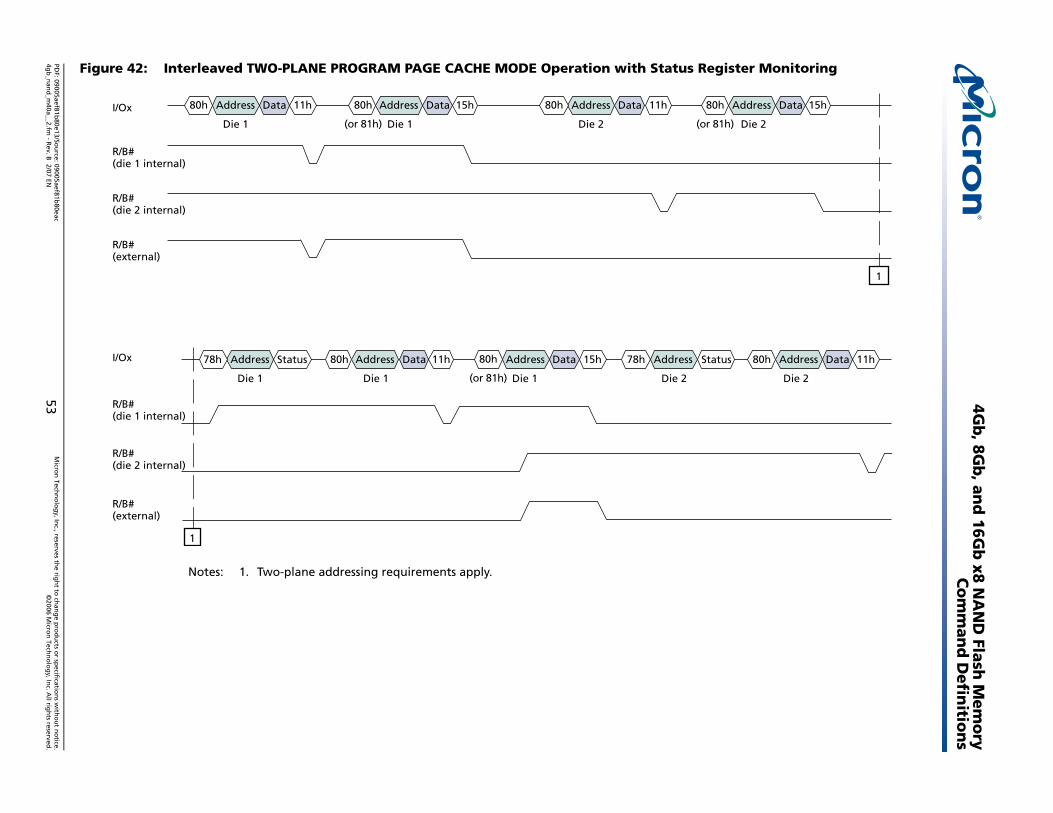
PDF: 09005aef81b
4gb
_nan
d_m
40a__2.fm-
Rev. B
2/07 EN53
©2006 M
icron
Techn
olo
gy, In
c. All rig
hts reserved
.
4Gb
, 8Gb
, and
16Gb
x8 NA
ND
Flash M
emo
ryC
om
man
d D
efinitio
ns
Figure 42: Interleaved TWO-PLANE PROGRAM PAGE CACHE MODE Operation with Status Register Monitoring
1
DataAddress80h 11h DataAddress80h 15h DataAddress80h 11h DataAddress 15h
DataAddressh 11h
Die 2
I/Ox 80h
80e13/Sou
rce: 09005aef81b80eac
Micro
n Tech
no
log
y, Inc., reserves th
e righ
t to ch
ang
e pro
du
cts or sp
ecification
s with
ou
t no
tice.
Notes: 1. Two-plane addressing requirements apply.
(or 81h)Die 1 Die 1 Die 2 Die 2
Address DataAddress80h 11h
Die 1 Die 1
DataAddress 15h Address
Die 1
80
Die 2
R/B#(die 1 internal)
R/B#(die 2 internal)
R/B#(external)
Status StatusI/Ox
R/B#(die 1 internal)
R/B#(die 2 internal)
R/B#(external)
78h78h
1
(or 81h)
80h
(or 81h)
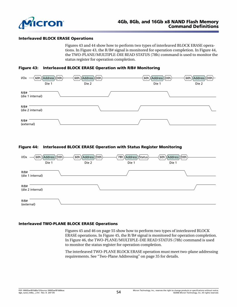
4Gb, 8Gb, and 16Gb x8 NAND Flash MemoryCommand Definitions
Interleaved BLOCK ERASE Operations
Figures 43 and 44 show how to perform two types of interleaved BLOCK ERASE opera-tions. In Figure 43, the R/B# signal is monitored for operation completion. In Figure 44, the TWO-PLANE/MULTIPLE-DIE READ STATUS (78h) command is used to monitor the status register for operation completion.
Figure 43: Interleaved BLOCK ERASE Operation with R/B# Monitoring
Figure 44: Interleaved BLOCK ERASE Operation with Status Register Monitoring
Interleaved TWO-PLANE BLOCK ERASE Operations
Figures 45 and 46 on page 55 show how to perform two types of interleaved BLOCK ERASE operations. In Figure 45, the R/B# signal is monitored for operation completion. In Figure 46, the TWO-PLANE/MULTIPLE-DIE READ STATUS (78h) command is used to monitor the status register for operation completion.
The interleaved TWO-PLANE BLOCK ERASE operation must meet two-plane addressing requirements. See “Two-Plane Addressing” on page 35 for details.
Address60h D0h
Die 1
Address60h D0h
Die 2
Address60h D0h
Die 1
Address60h D0h
Die 2
I/Ox
R/B#(die 1 internal)
R/B#(die 2 internal)
R/B#(external)
Address60h D0h
Die 1
Address60h D0h
Die 2
Address Status
Die 1
Address60h D0h
Die 1
I/Ox
R/B#(die 1 internal)
R/B#(die 2 internal)
R/B#(external)
78h
PDF: 09005aef81b80e13/Source: 09005aef81b80eac Micron Technology, Inc., reserves the right to change products or specifications without notice.4gb_nand_m40a__2.fm - Rev. B 2/07 EN 54 ©2006 Micron Technology, Inc. All rights reserved.
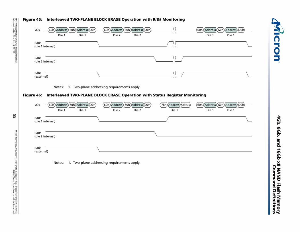
PDF: 09005aef81b
4gb
_nan
d_m
40a__2.fm-
Rev. B
2/07 EN55
©2006 M
icron
Techn
olo
gy, In
c. All rig
hts reserved
.
4Gb
, 8Gb
, and
16Gb
x8 NA
ND
Flash M
emo
ryC
om
man
d D
efinitio
ns
Figure 45: Interleaved TWO-PLANE BLOCK ERASE Operation with R/B# Monitoring
Address60h Address60h D0h Address60h Address60h D0h 60h Address Address60h60h
Die 1
I/Ox D0h
Address60h
Die 1
D0h
80e13/Sou
rce: 09005aef81b80eac
Micro
n Tech
no
log
y, Inc., reserves th
e righ
t to ch
ang
e pro
du
cts or sp
ecification
s with
ou
t no
tice.
Notes: 1. Two-plane addressing requirements apply.
Figure 46: Interleaved TWO-PLANE BLOCK ERASE Operation with Status Register Monitoring
Notes: 1. Two-plane addressing requirements apply.
Die 1 Die 1 Die 2 Die 2 Die 1
R/B#(die 1 internal)
R/B#(die 2 internal)
R/B#(external)
Address60h
Die 1
Address60h D0h
Die 1
Address60h
Die 2
Address60h D0h Address 60h
Die 2
Address
Die 1Die 1
60hI/Ox
R/B#(die 1 internal)
R/B#(die 2 internal)
R/B#(external)
78h Status
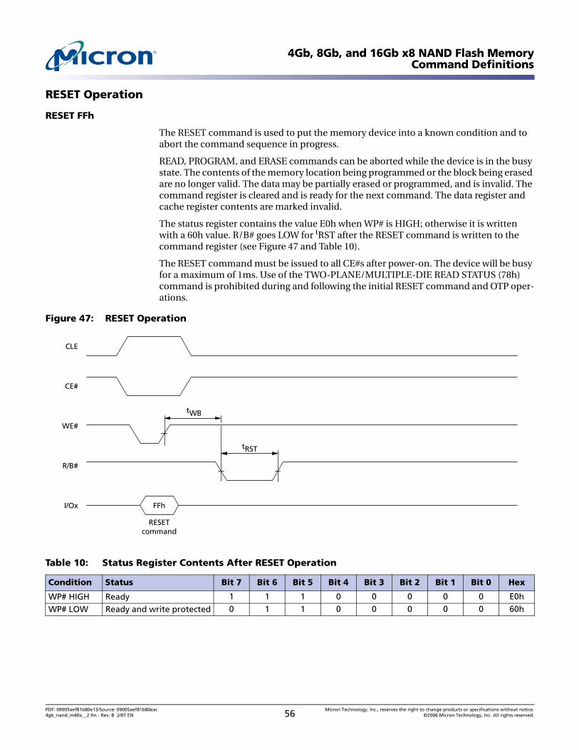
4Gb, 8Gb, and 16Gb x8 NAND Flash MemoryCommand Definitions
RESET Operation
RESET FFh
The RESET command is used to put the memory device into a known condition and to abort the command sequence in progress.
READ, PROGRAM, and ERASE commands can be aborted while the device is in the busy state. The contents of the memory location being programmed or the block being erased are no longer valid. The data may be partially erased or programmed, and is invalid. The command register is cleared and is ready for the next command. The data register and cache register contents are marked invalid.
The status register contains the value E0h when WP# is HIGH; otherwise it is written with a 60h value. R/B# goes LOW for tRST after the RESET command is written to the command register (see Figure 47 and Table 10).
The RESET command must be issued to all CE#s after power-on. The device will be busy for a maximum of 1ms. Use of the TWO-PLANE/MULTIPLE-DIE READ STATUS (78h) command is prohibited during and following the initial RESET command and OTP oper-ations.
Figure 47: RESET Operation
Table 10: Status Register Contents After RESET Operation
Condition Status Bit 7 Bit 6 Bit 5 Bit 4 Bit 3 Bit 2 Bit 1 Bit 0 Hex
WP# HIGH Ready 1 1 1 0 0 0 0 0 E0h
WP# LOW Ready and write protected 0 1 1 0 0 0 0 0 60h
CLE
CE#
WE#
R/B#
I/Ox
tRST
tWB
FFh
RESETcommand
PDF: 09005aef81b80e13/Source: 09005aef81b80eac Micron Technology, Inc., reserves the right to change products or specifications without notice.4gb_nand_m40a__2.fm - Rev. B 2/07 EN 56 ©2006 Micron Technology, Inc. All rights reserved.
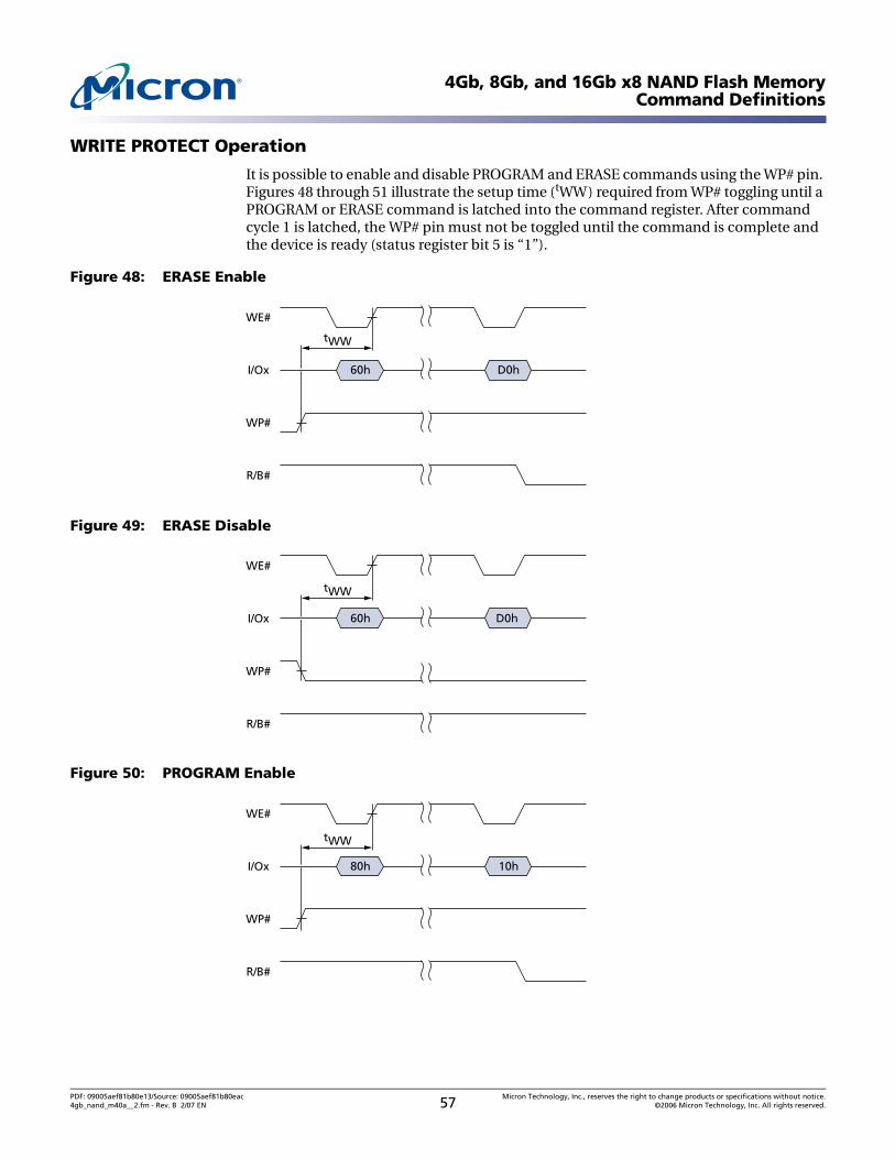
4Gb, 8Gb, and 16Gb x8 NAND Flash MemoryCommand Definitions
WRITE PROTECT Operation
It is possible to enable and disable PROGRAM and ERASE commands using the WP# pin. Figures 48 through 51 illustrate the setup time (tWW) required from WP# toggling until a PROGRAM or ERASE command is latched into the command register. After command cycle 1 is latched, the WP# pin must not be toggled until the command is complete and the device is ready (status register bit 5 is “1”).
Figure 48: ERASE Enable
Figure 49: ERASE Disable
Figure 50: PROGRAM Enable
tWW
60h D0h
WE#
I/Ox
WP#
R/B#
tWW
60h D0h
WE#
I/Ox
WP#
R/B#
tWW
80h 10h
WE#
I/Ox
WP#
R/B#
PDF: 09005aef81b80e13/Source: 09005aef81b80eac Micron Technology, Inc., reserves the right to change products or specifications without notice.4gb_nand_m40a__2.fm - Rev. B 2/07 EN 57 ©2006 Micron Technology, Inc. All rights reserved.
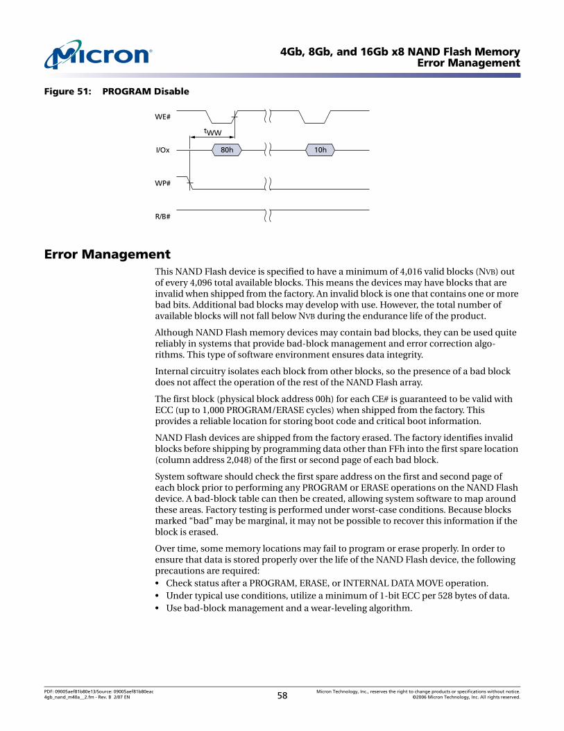
4Gb, 8Gb, and 16Gb x8 NAND Flash MemoryError Management
Figure 51: PROGRAM Disable
Error ManagementThis NAND Flash device is specified to have a minimum of 4,016 valid blocks (NVB) out of every 4,096 total available blocks. This means the devices may have blocks that are invalid when shipped from the factory. An invalid block is one that contains one or more bad bits. Additional bad blocks may develop with use. However, the total number of available blocks will not fall below NVB during the endurance life of the product.
Although NAND Flash memory devices may contain bad blocks, they can be used quite reliably in systems that provide bad-block management and error correction algo-rithms. This type of software environment ensures data integrity.
Internal circuitry isolates each block from other blocks, so the presence of a bad block does not affect the operation of the rest of the NAND Flash array.
The first block (physical block address 00h) for each CE# is guaranteed to be valid with ECC (up to 1,000 PROGRAM/ERASE cycles) when shipped from the factory. This provides a reliable location for storing boot code and critical boot information.
NAND Flash devices are shipped from the factory erased. The factory identifies invalid blocks before shipping by programming data other than FFh into the first spare location (column address 2,048) of the first or second page of each bad block.
System software should check the first spare address on the first and second page of each block prior to performing any PROGRAM or ERASE operations on the NAND Flash device. A bad-block table can then be created, allowing system software to map around these areas. Factory testing is performed under worst-case conditions. Because blocks marked “bad” may be marginal, it may not be possible to recover this information if the block is erased.
Over time, some memory locations may fail to program or erase properly. In order to ensure that data is stored properly over the life of the NAND Flash device, the following precautions are required:• Check status after a PROGRAM, ERASE, or INTERNAL DATA MOVE operation.• Under typical use conditions, utilize a minimum of 1-bit ECC per 528 bytes of data.• Use bad-block management and a wear-leveling algorithm.
tWW
80h 10h
WE#
I/Ox
WP#
R/B#
PDF: 09005aef81b80e13/Source: 09005aef81b80eac Micron Technology, Inc., reserves the right to change products or specifications without notice.4gb_nand_m40a__2.fm - Rev. B 2/07 EN 58 ©2006 Micron Technology, Inc. All rights reserved.
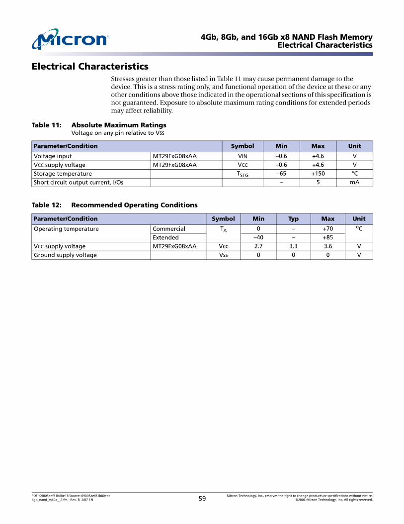
4Gb, 8Gb, and 16Gb x8 NAND Flash MemoryElectrical Characteristics
Electrical CharacteristicsStresses greater than those listed in Table 11 may cause permanent damage to the device. This is a stress rating only, and functional operation of the device at these or any other conditions above those indicated in the operational sections of this specification is not guaranteed. Exposure to absolute maximum rating conditions for extended periods may affect reliability.
Table 11: Absolute Maximum RatingsVoltage on any pin relative to VSS
Parameter/Condition Symbol Min Max Unit
Voltage input MT29FxG08xAA VIN –0.6 +4.6 V
VCC supply voltage MT29FxG08xAA VCC –0.6 +4.6 V
Storage temperature TSTG –65 +150 °C
Short circuit output current, I/Os – 5 mA
Table 12: Recommended Operating Conditions
Parameter/Condition Symbol Min Typ Max Unit
Operating temperature Commercial TA 0 – +70 oC
Extended –40 – +85
VCC supply voltage MT29FxG08xAA Vcc 2.7 3.3 3.6 V
Ground supply voltage Vss 0 0 0 V
PDF: 09005aef81b80e13/Source: 09005aef81b80eac Micron Technology, Inc., reserves the right to change products or specifications without notice.4gb_nand_m40a__2.fm - Rev. B 2/07 EN 59 ©2006 Micron Technology, Inc. All rights reserved.
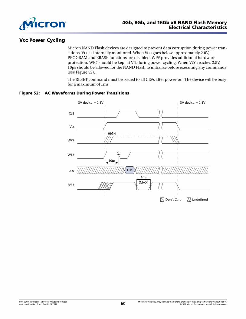
4Gb, 8Gb, and 16Gb x8 NAND Flash MemoryElectrical Characteristics
VCC Power Cycling
Micron NAND Flash devices are designed to prevent data corruption during power tran-sitions. VCC is internally monitored. When VCC goes below approximately 2.0V, PROGRAM and ERASE functions are disabled. WP# provides additional hardware protection. WP# should be kept at VIL during power cycling. When VCC reaches 2.5V, 10µs should be allowed for the NAND Flash to initialize before executing any commands (see Figure 52).
The RESET command must be issued to all CE#s after power-on. The device will be busy for a maximum of 1ms.
Figure 52: AC Waveforms During Power Transitions
WE#
R/B#
WP#
VCC
10µs
HIGH
3V device: ≈ 2.5V 3V device: ≈ 2.5V
UndefinedDon’t Care
I/Ox FFh
CLE
1ms
(MAX)
PDF: 09005aef81b80e13/Source: 09005aef81b80eac Micron Technology, Inc., reserves the right to change products or specifications without notice.4gb_nand_m40a__2.fm - Rev. B 2/07 EN 60 ©2006 Micron Technology, Inc. All rights reserved.
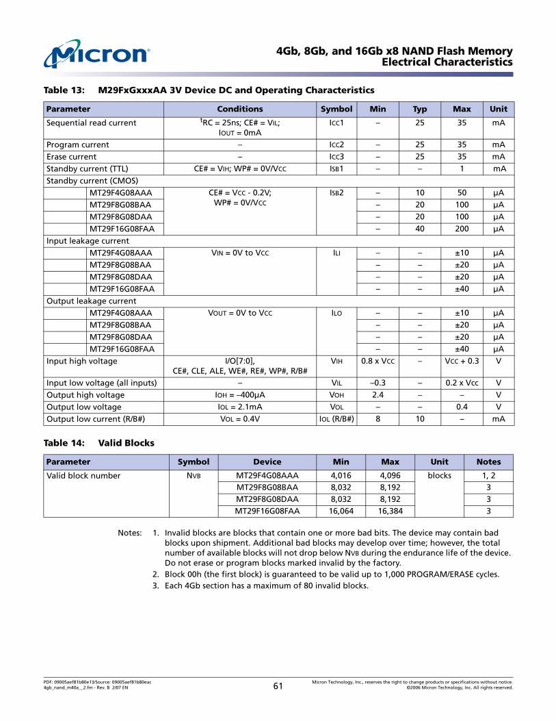
4Gb, 8Gb, and 16Gb x8 NAND Flash MemoryElectrical Characteristics
Notes: 1. Invalid blocks are blocks that contain one or more bad bits. The device may contain bad blocks upon shipment. Additional bad blocks may develop over time; however, the total number of available blocks will not drop below NVB during the endurance life of the device. Do not erase or program blocks marked invalid by the factory.
2. Block 00h (the first block) is guaranteed to be valid up to 1,000 PROGRAM/ERASE cycles.3. Each 4Gb section has a maximum of 80 invalid blocks.
Table 13: M29FxGxxxAA 3V Device DC and Operating Characteristics
Parameter Conditions Symbol Min Typ Max Unit
Sequential read current tRC = 25ns; CE# = VIL;IOUT = 0mA
ICC1 – 25 35 mA
Program current – ICC2 – 25 35 mA
Erase current – ICC3 – 25 35 mA
Standby current (TTL) CE# = VIH; WP# = 0V/VCC ISB1 – – 1 mA
Standby current (CMOS)MT29F4G08AAA CE# = VCC - 0.2V;
WP# = 0V/VCC
ISB2 – 10 50 µA
MT29F8G08BAA – 20 100 µA
MT29F8G08DAA – 20 100 µA
MT29F16G08FAA – 40 200 µA
Input leakage currentMT29F4G08AAA VIN = 0V to VCC ILI – – ±10 µA
MT29F8G08BAA – – ±20 µA
MT29F8G08DAA – – ±20 µA
MT29F16G08FAA – – ±40 µA
Output leakage currentMT29F4G08AAA VOUT = 0V to VCC ILO – – ±10 µA
MT29F8G08BAA – – ±20 µA
MT29F8G08DAA – – ±20 µA
MT29F16G08FAA – – ±40 µA
Input high voltage I/O[7:0],CE#, CLE, ALE, WE#, RE#, WP#, R/B#
VIH 0.8 x VCC – VCC + 0.3 V
Input low voltage (all inputs) – VIL –0.3 – 0.2 x Vcc V
Output high voltage IOH = –400µA VOH 2.4 – – V
Output low voltage IOL = 2.1mA VOL – – 0.4 V
Output low current (R/B#) VOL = 0.4V IOL (R/B#) 8 10 – mA
Table 14: Valid Blocks
Parameter Symbol Device Min Max Unit Notes
Valid block number NVB MT29F4G08AAA 4,016 4,096 blocks 1, 2MT29F8G08BAA 8,032 8,192 3MT29F8G08DAA 8,032 8,192 3MT29F16G08FAA 16,064 16,384 3
PDF: 09005aef81b80e13/Source: 09005aef81b80eac Micron Technology, Inc., reserves the right to change products or specifications without notice.4gb_nand_m40a__2.fm - Rev. B 2/07 EN 61 ©2006 Micron Technology, Inc. All rights reserved.
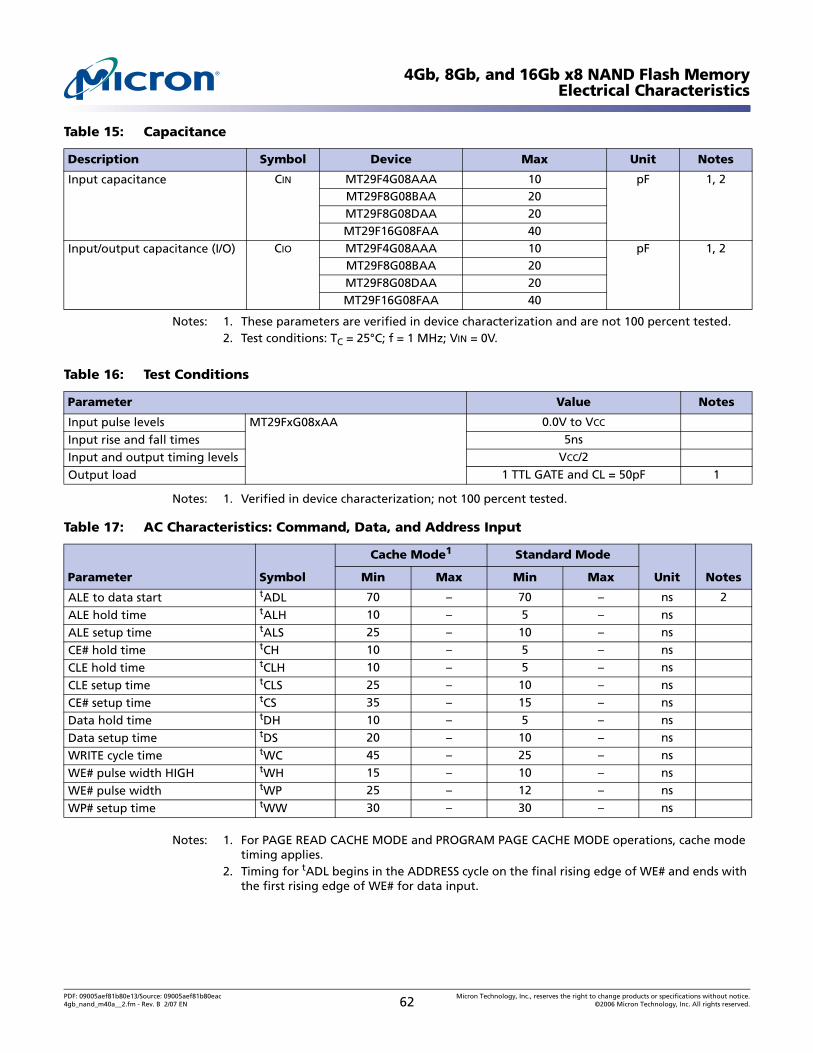
4Gb, 8Gb, and 16Gb x8 NAND Flash MemoryElectrical Characteristics
Notes: 1. These parameters are verified in device characterization and are not 100 percent tested.2. Test conditions: TC = 25°C; f = 1 MHz; VIN = 0V.
Notes: 1. Verified in device characterization; not 100 percent tested.
Notes: 1. For PAGE READ CACHE MODE and PROGRAM PAGE CACHE MODE operations, cache mode timing applies.
2. Timing for tADL begins in the ADDRESS cycle on the final rising edge of WE# and ends with the first rising edge of WE# for data input.
Table 15: Capacitance
Description Symbol Device Max Unit Notes
Input capacitance CIN MT29F4G08AAA 10 pF 1, 2MT29F8G08BAA 20MT29F8G08DAA 20MT29F16G08FAA 40
Input/output capacitance (I/O) CIO MT29F4G08AAA 10 pF 1, 2MT29F8G08BAA 20MT29F8G08DAA 20MT29F16G08FAA 40
Table 16: Test Conditions
Parameter Value Notes
Input pulse levels MT29FxG08xAA 0.0V to VCC
Input rise and fall times 5ns
Input and output timing levels VCC/2
Output load 1 TTL GATE and CL = 50pF 1
Table 17: AC Characteristics: Command, Data, and Address Input
Parameter Symbol
Cache Mode1 Standard Mode
Unit NotesMin Max Min Max
ALE to data start tADL 70 – 70 – ns 2
ALE hold time tALH 10 – 5 – ns
ALE setup time tALS 25 – 10 – ns
CE# hold time tCH 10 – 5 – ns
CLE hold time tCLH 10 – 5 – ns
CLE setup time tCLS 25 – 10 – ns
CE# setup time tCS 35 – 15 – ns
Data hold time tDH 10 – 5 – ns
Data setup time tDS 20 – 10 – ns
WRITE cycle time tWC 45 – 25 – ns
WE# pulse width HIGH tWH 15 – 10 – ns
WE# pulse width tWP 25 – 12 – ns
WP# setup time tWW 30 – 30 – ns
PDF: 09005aef81b80e13/Source: 09005aef81b80eac Micron Technology, Inc., reserves the right to change products or specifications without notice.4gb_nand_m40a__2.fm - Rev. B 2/07 EN 62 ©2006 Micron Technology, Inc. All rights reserved.
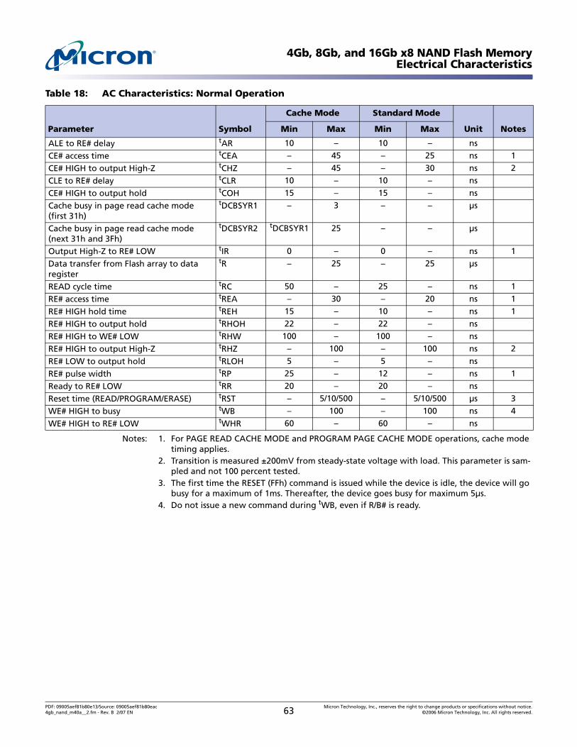
4Gb, 8Gb, and 16Gb x8 NAND Flash MemoryElectrical Characteristics
Notes: 1. For PAGE READ CACHE MODE and PROGRAM PAGE CACHE MODE operations, cache mode timing applies.
2. Transition is measured ±200mV from steady-state voltage with load. This parameter is sam-pled and not 100 percent tested.
3. The first time the RESET (FFh) command is issued while the device is idle, the device will go busy for a maximum of 1ms. Thereafter, the device goes busy for maximum 5µs.
4. Do not issue a new command during tWB, even if R/B# is ready.
Table 18: AC Characteristics: Normal Operation
Parameter Symbol
Cache Mode Standard Mode
Unit NotesMin Max Min Max
ALE to RE# delay tAR 10 – 10 – ns
CE# access time tCEA – 45 – 25 ns 1
CE# HIGH to output High-Z tCHZ – 45 – 30 ns 2
CLE to RE# delay tCLR 10 – 10 – ns
CE# HIGH to output hold tCOH 15 – 15 – ns
Cache busy in page read cache mode (first 31h)
tDCBSYR1 – 3 – – µs
Cache busy in page read cache mode (next 31h and 3Fh)
tDCBSYR2 tDCBSYR1 25 – – µs
Output High-Z to RE# LOW tIR 0 – 0 – ns 1
Data transfer from Flash array to data register
tR – 25 – 25 µs
READ cycle time tRC 50 – 25 – ns 1
RE# access time tREA – 30 – 20 ns 1
RE# HIGH hold time tREH 15 – 10 – ns 1
RE# HIGH to output hold tRHOH 22 – 22 – ns
RE# HIGH to WE# LOW tRHW 100 – 100 – ns
RE# HIGH to output High-Z tRHZ – 100 – 100 ns 2
RE# LOW to output hold tRLOH 5 – 5 – ns
RE# pulse width tRP 25 – 12 – ns 1
Ready to RE# LOW tRR 20 – 20 – ns
Reset time (READ/PROGRAM/ERASE) tRST – 5/10/500 – 5/10/500 µs 3
WE# HIGH to busy tWB – 100 – 100 ns 4
WE# HIGH to RE# LOW tWHR 60 – 60 – ns
PDF: 09005aef81b80e13/Source: 09005aef81b80eac Micron Technology, Inc., reserves the right to change products or specifications without notice.4gb_nand_m40a__2.fm - Rev. B 2/07 EN 63 ©2006 Micron Technology, Inc. All rights reserved.
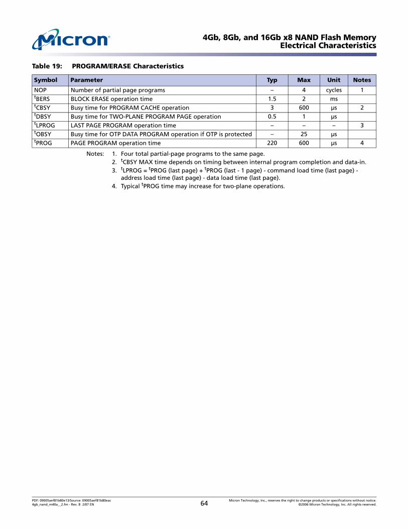
4Gb, 8Gb, and 16Gb x8 NAND Flash MemoryElectrical Characteristics
Notes: 1. Four total partial-page programs to the same page.2. tCBSY MAX time depends on timing between internal program completion and data-in.3. tLPROG = tPROG (last page) + tPROG (last - 1 page) - command load time (last page) -
address load time (last page) - data load time (last page).4. Typical tPROG time may increase for two-plane operations.
Table 19: PROGRAM/ERASE Characteristics
Symbol Parameter Typ Max Unit Notes
NOP Number of partial page programs – 4 cycles 1tBERS BLOCK ERASE operation time 1.5 2 mstCBSY Busy time for PROGRAM CACHE operation 3 600 µs 2tDBSY Busy time for TWO-PLANE PROGRAM PAGE operation 0.5 1 µstLPROG LAST PAGE PROGRAM operation time – – – 3tOBSY Busy time for OTP DATA PROGRAM operation if OTP is protected – 25 µstPROG PAGE PROGRAM operation time 220 600 µs 4
PDF: 09005aef81b80e13/Source: 09005aef81b80eac Micron Technology, Inc., reserves the right to change products or specifications without notice.4gb_nand_m40a__2.fm - Rev. B 2/07 EN 64 ©2006 Micron Technology, Inc. All rights reserved.
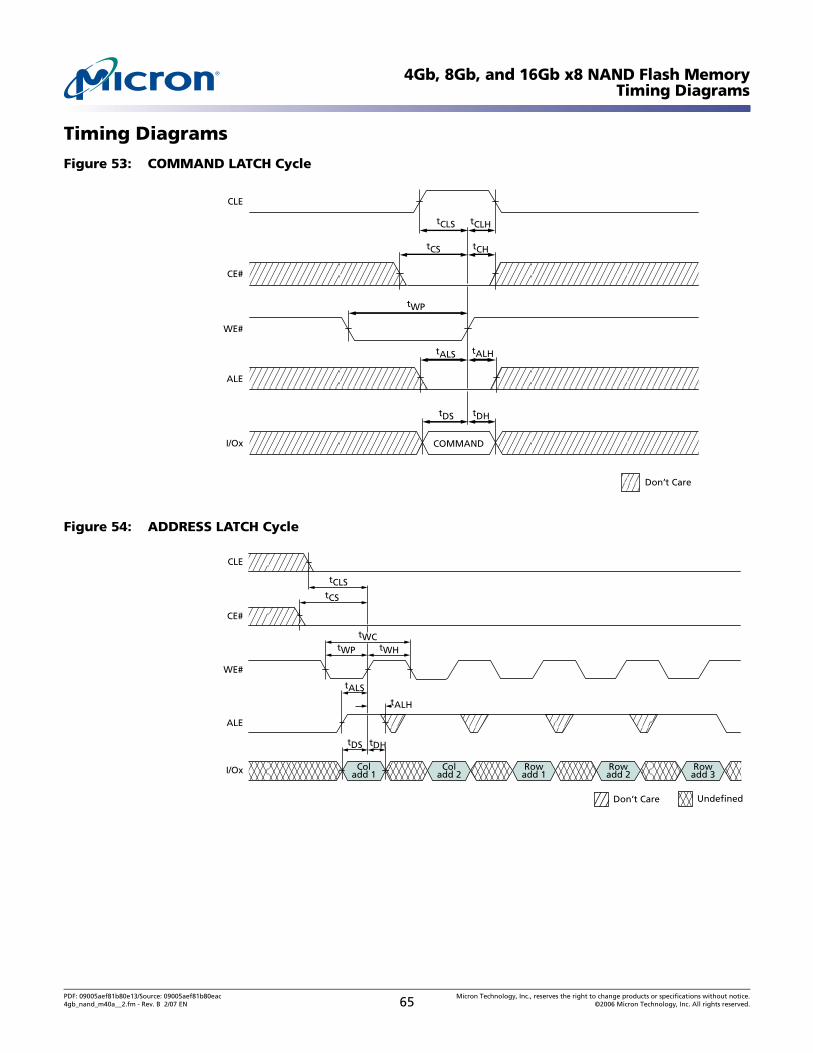
4Gb, 8Gb, and 16Gb x8 NAND Flash MemoryTiming Diagrams
Timing Diagrams
Figure 53: COMMAND LATCH Cycle
Figure 54: ADDRESS LATCH Cycle
WE#
CE#
ALE
CLE
I/Ox COMMAND
tWP
tCHtCS
tALH
tDHtDS
tALS
tCLHtCLS
Don’t Care
WE#
CE#
ALE
CLE
I/Ox Coladd 1
tWP tWH
tCS
tDHtDS
tALS
tALH
tCLS
Coladd 2
Rowadd 1
Rowadd 2
Rowadd 3
Don’t Care Undefined
tWC
PDF: 09005aef81b80e13/Source: 09005aef81b80eac Micron Technology, Inc., reserves the right to change products or specifications without notice.4gb_nand_m40a__2.fm - Rev. B 2/07 EN 65 ©2006 Micron Technology, Inc. All rights reserved.
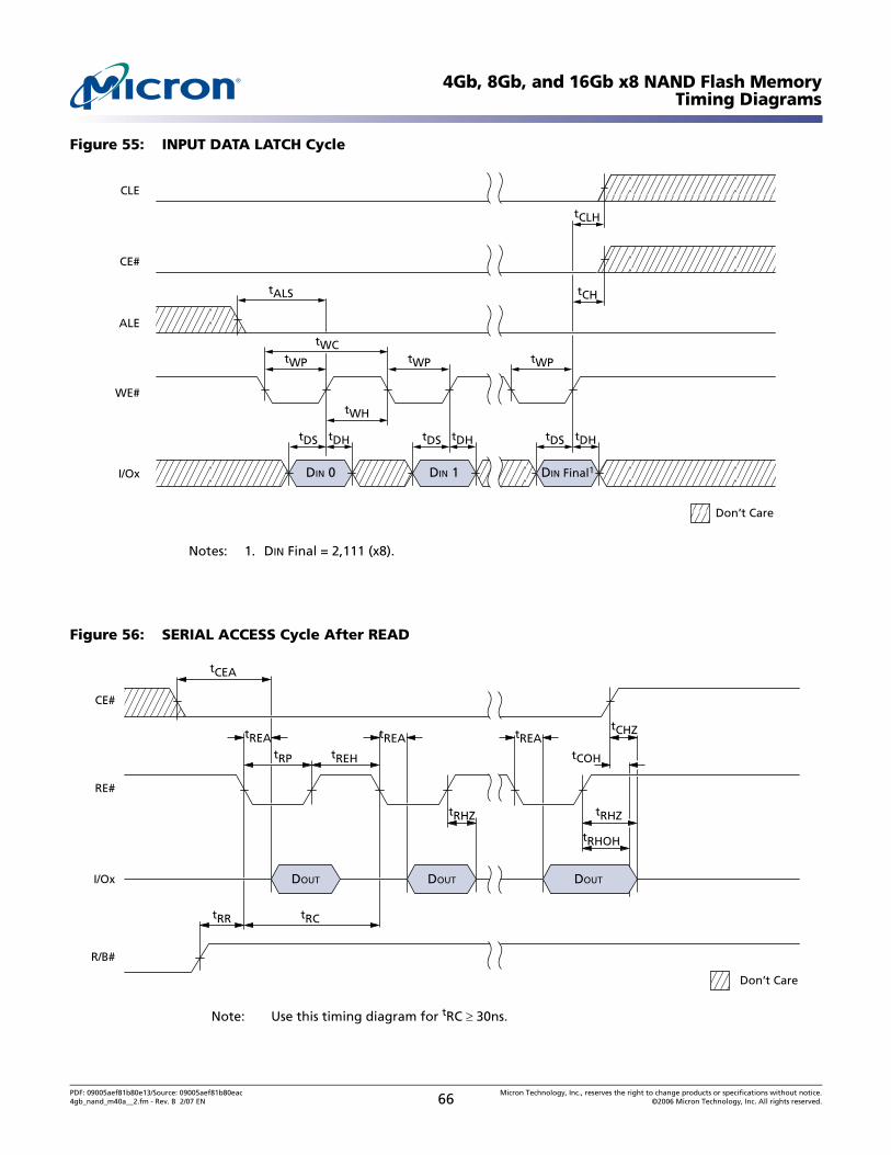
4Gb, 8Gb, and 16Gb x8 NAND Flash MemoryTiming Diagrams
Figure 55: INPUT DATA LATCH Cycle
Notes: 1. DIN Final = 2,111 (x8).
Figure 56: SERIAL ACCESS Cycle After READ
Note: Use this timing diagram for tRC ≥ 30ns.
WE#
CE#
ALE
CLE
I/Ox
tWP tWP tWP
tWH
tALS
tDHtDS tDHtDS tDHtDS
tCLH
tCH
DIN 1 DIN Final1
Don’t Care
tWC
DIN 0
CE#
RE#
I/Ox
tREHtRP
tRR tRC
tCEA
tREA tREA tREA
Don’t Care
tRHZ
tCHZ
tRHZ
tRHOH
R/B#
tCOH
DOUT DOUTDOUT
PDF: 09005aef81b80e13/Source: 09005aef81b80eac Micron Technology, Inc., reserves the right to change products or specifications without notice.4gb_nand_m40a__2.fm - Rev. B 2/07 EN 66 ©2006 Micron Technology, Inc. All rights reserved.
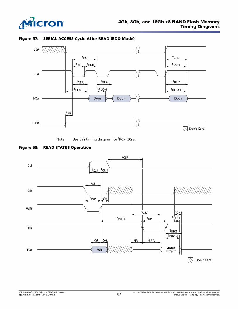
4Gb, 8Gb, and 16Gb x8 NAND Flash MemoryTiming Diagrams
Figure 57: SERIAL ACCESS Cycle After READ (EDO Mode)
Note: Use this timing diagram for tRC < 30ns.
Figure 58: READ STATUS Operation
DOUT DOUT
CE#
RE#
I/Ox
R/B#
tRR
tCEA
tREA
tRP tREH
tRC
tRLOH
tREA
tRHOH
tRHZ
tCOH
tCHZ
Don’t Care
DOUT
RE#
CE#
WE#
CLE
I/Ox
tRHZ
tWP
tWHR
tCLR
tCH
tCLS
tCS
tCLH
tDH
tRP
tCHZ
tDS tREA
tRHOHtIR
70h Statusoutput
Don’t Care
tCEAtCOH
PDF: 09005aef81b80e13/Source: 09005aef81b80eac Micron Technology, Inc., reserves the right to change products or specifications without notice.4gb_nand_m40a__2.fm - Rev. B 2/07 EN 67 ©2006 Micron Technology, Inc. All rights reserved.
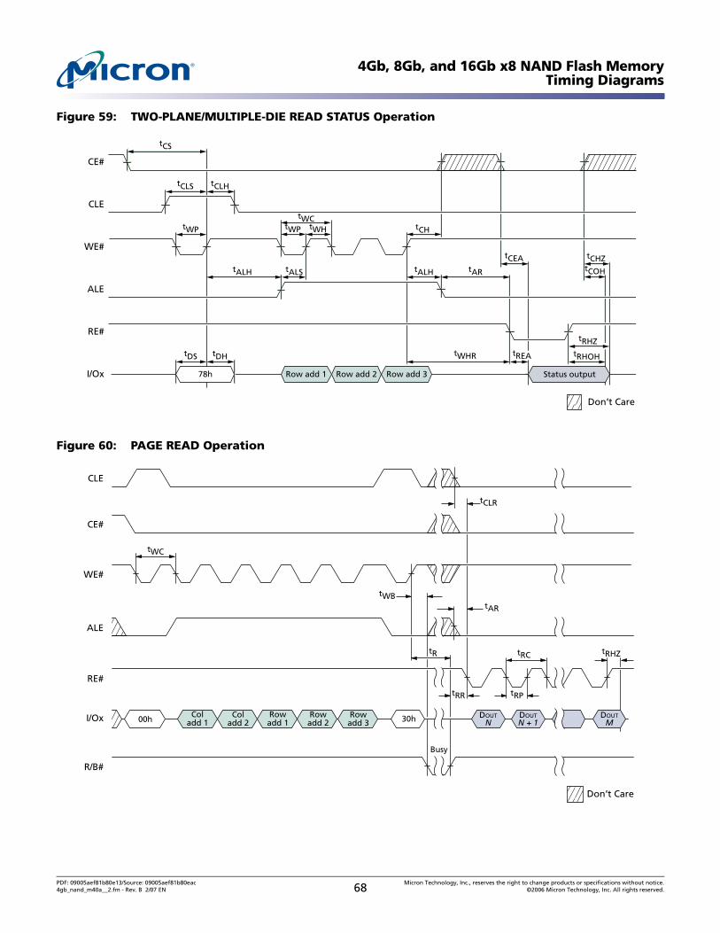
4Gb, 8Gb, and 16Gb x8 NAND Flash MemoryTiming Diagrams
Figure 59: TWO-PLANE/MULTIPLE-DIE READ STATUS Operation
Figure 60: PAGE READ Operation
tWHR
tAR
CE#
CLE
WE#
ALE
RE#
I/Ox
Don’t Care
78h Row add 1 Row add 2 Row add 3 Status output
tDS tDH
tWP tWP
tWCtCH
tALS tALH
tWH
tCLS tCLH
tALH
tCS
tCEA tCHZ
tREA tRHOH
tRHZ
tCOH
DOUTN
DOUTN + 1
DOUTM
WE#
CE#
ALE
CLE
RE#
R/B#
I/Ox
tWC
Busy
00h 30h
tR
tWBtAR
tRR tRP
tCLR
tRC tRHZ
Don’t Care
Coladd 1
Coladd 2
Rowadd 1
Rowadd 2
Rowadd 3
PDF: 09005aef81b80e13/Source: 09005aef81b80eac Micron Technology, Inc., reserves the right to change products or specifications without notice.4gb_nand_m40a__2.fm - Rev. B 2/07 EN 68 ©2006 Micron Technology, Inc. All rights reserved.
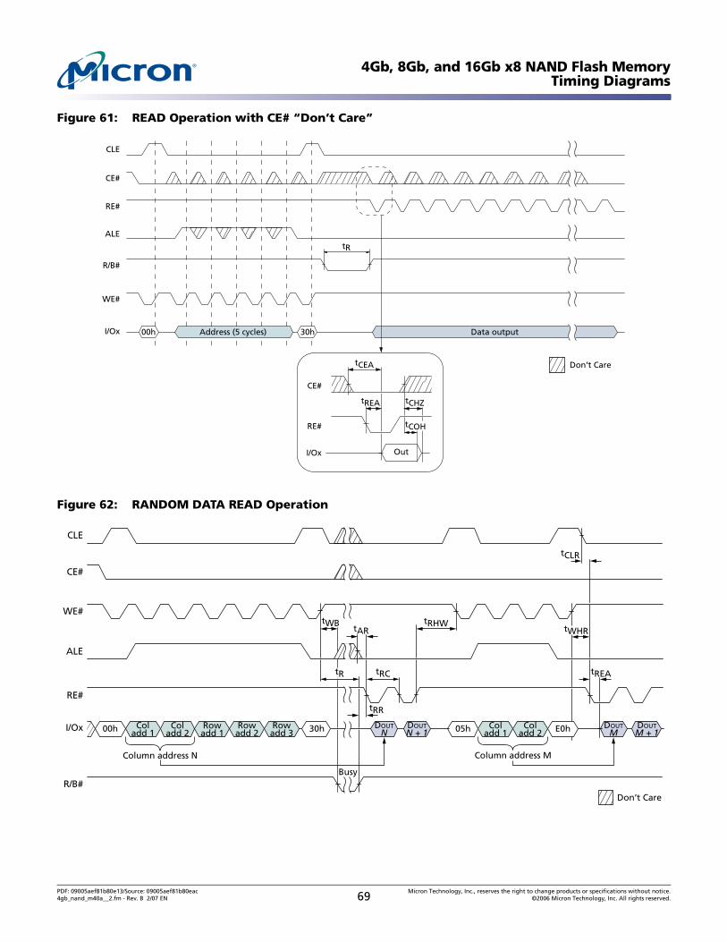
4Gb, 8Gb, and 16Gb x8 NAND Flash MemoryTiming Diagrams
Figure 61: READ Operation with CE# “Don’t Care”
Figure 62: RANDOM DATA READ Operation
RE#
CE#
tREA tCHZ
tCEA
RE#
CE#
ALE
CLE
I/Ox
I/Ox Out
R/B#
WE#
Data output
tR
Don’t Care
Address (5 cycles)00h 30h
tCOH
WE#
CE#
ALE
CLE
RE#
R/B#
I/Ox
Busy
Coladd 1
Coladd 2
Rowadd 1
Rowadd 2
Rowadd 300h
tWBtAR
tRR
Don’t Care
tRC
tRHW
DOUTM
DOUTM + 1
Coladd 1
Coladd 205h E0h
tREA
tCLR
DOUTN
DOUTN + 130h
tWHR
Column address N Column address M
tR
PDF: 09005aef81b80e13/Source: 09005aef81b80eac Micron Technology, Inc., reserves the right to change products or specifications without notice.4gb_nand_m40a__2.fm - Rev. B 2/07 EN 69 ©2006 Micron Technology, Inc. All rights reserved.
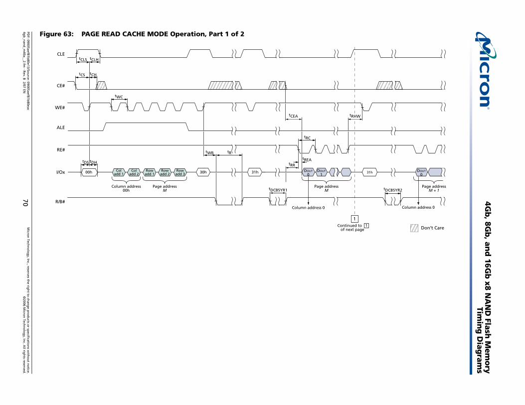
PDF: 09005aef81b
4gb
_nan
d_m
40a__2.fm-
Rev. B
2/07 EN70
©2006 M
icron
Techn
olo
gy, In
c. All rig
hts reserved
.
4Gb
, 8Gb
, and
16Gb
x8 NA
ND
Flash M
emo
ryTim
ing
Diag
rams
Figure 63: PAGE READ CACHE MODE Operation, Part 1 of 2
CLE
Don’t Care
tDCBSYR2
Column address 0
DOUT0
Page addressM + 1
80e13/Sou
rce: 09005aef81b80eac
Micro
n Tech
no
log
y, Inc., reserves th
e righ
t to ch
ang
e pro
du
cts or sp
ecification
s with
ou
t no
tice.
tWC
WE#
CE#
ALE
RE#
R/B#
I/Ox
Column address 0
1
DOUT
Page addressM
Page addressM
Column address00h
tCEA
tDS
tCLHtCLS
tCS tCH
tDH tRR
tWB
Continued to 1of next page
tRC
tREA
30h DOUT0
DOUT1
31h 31hColadd 2
Rowadd 1
Rowadd 2
Rowadd 300h
tDCBSYR1
Coladd 1
tRHW
tR
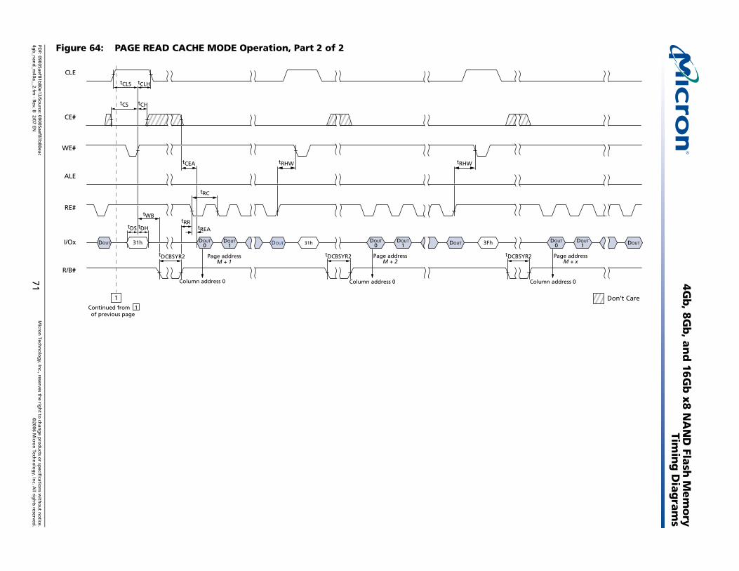
PDF: 09005aef81b
4gb
_nan
d_m
40a__2.fm-
Rev. B
2/07 EN71
©2006 M
icron
Techn
olo
gy, In
c. All rig
hts reserved
.
4Gb
, 8Gb
, and
16Gb
x8 NA
ND
Flash M
emo
ryTim
ing
Diag
rams
Figure 64: PAGE READ CACHE MODE Operation, Part 2 of 2
CLE
Don’t Care
Page addressM + x
lumn address 0
DOUT0 DOUTDOUT
1
80e13/Sou
rce: 09005aef81b80eac
Micro
n Tech
no
log
y, Inc., reserves th
e righ
t to ch
ang
e pro
du
cts or sp
ecification
s with
ou
t no
tice.
WE#
CE#
ALE
RE#
R/B#
I/Ox
1
Page addressM + 1
Page addressM + 2
Column address 0
Continued from 1of previous page
Co
tCLH
tCH
tREA
tCEA tRHW
tDS tDHtRR
tDCBSYR2 tDCBSYR2
tWB
Column address 0
31h DOUT0 DOUT 3FhDOUT
1
tCLS
tCS
tRC
DOUT 31h
tDCBSYR2
tRHW
DOUT1 DOUTDOUT
0
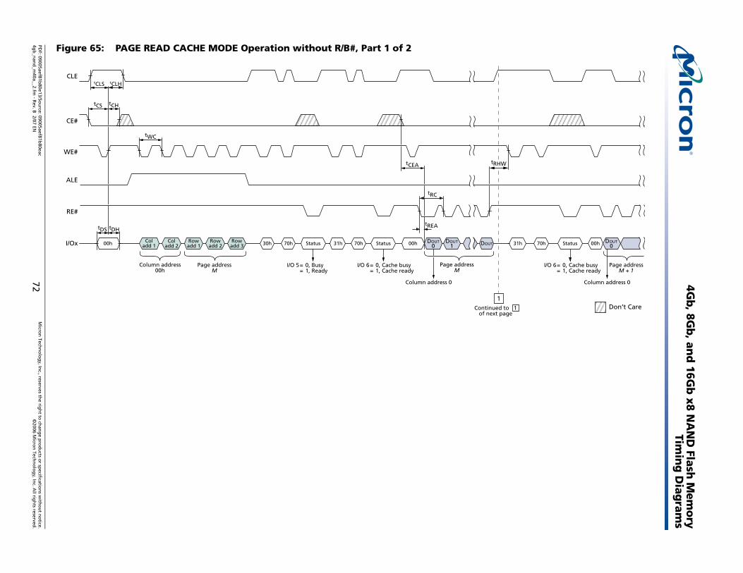
PDF: 09005aef81b
4gb
_nan
d_m
40a__2.fm-
Rev. B
2/07 EN72
©2006 M
icron
Techn
olo
gy, In
c. All rig
hts reserved
.
4Gb
, 8Gb
, and
16Gb
x8 NA
ND
Flash M
emo
ryTim
ing
Diag
rams
Figure 65: PAGE READ CACHE MODE Operation without R/B#, Part 1 of 2
CLE
DOUT0
Don’t Care
Column address 0
0h Status
I/O 6 = 0, Cache busy = 1, Cache ready
00h
Page addressM + 1
80e13/Sou
rce: 09005aef81b80eac
Micro
n Tech
no
log
y, Inc., reserves th
e righ
t to ch
ang
e pro
du
cts or sp
ecification
s with
ou
t no
tice.
tWC
WE#
CE#
ALE
RE#
I/Ox 30h 70h Status DOUT0
Column address 0
1
DOUT1 DOUT
Column address00h
Page addressM
Page addressM
tCEA
tDS
tCLHtCLS
tCS tCH
tDH
31h 31h 7
I/O 5 = 0, Busy = 1, Ready
Continued to 1of next page
Coladd 1
Coladd 2
Rowadd 1
Rowadd 2
Rowadd 300h 00h
tRC
tREA
70h Status
I/O 6 = 0, Cache busy = 1, Cache ready
tRHW
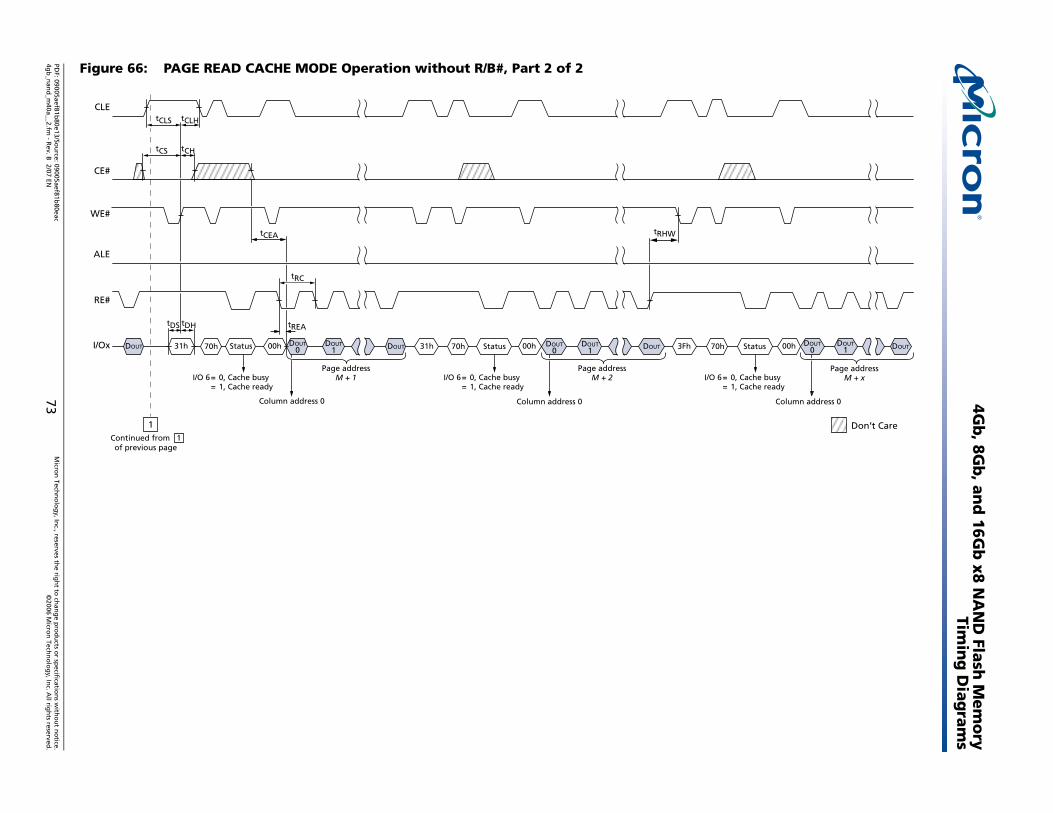
PDF: 09005aef81b
4gb
_nan
d_m
40a__2.fm-
Rev. B
2/07 EN73
©2006 M
icron
Techn
olo
gy, In
c. All rig
hts reserved
.
4Gb
, 8Gb
, and
16Gb
x8 NA
ND
Flash M
emo
ryTim
ing
Diag
rams
Figure 66: PAGE READ CACHE MODE Operation without R/B#, Part 2 of 2
CLE
Don’t Care
Page addressM + x
Column address 0
DOUTDOUT1
DOUT0s
busyready
00h
80e13/Sou
rce: 09005aef81b80eac
Micro
n Tech
no
log
y, Inc., reserves th
e righ
t to ch
ang
e pro
du
cts or sp
ecification
s with
ou
t no
tice.
WE#
CE#
ALE
RE#
I/Ox
1
Page addressM + 1
Page addressM + 2
Column address 0
Continued from 1of previous page
tREA
tCEA
tDS tDH
Column address 0
DOUT0
DOUT1 DOUT 31h DOUT
0 DOUT 3FhDOUT1
tRC
DOUT 31h 70h Status
I/O 6 = 0, Cache busy = 1, Cache ready
70h Status
I/O 6 = 0, Cache busy = 1, Cache ready
70h Statu
I/O 6 = 0, Cache = 1, Cache
00h00h
tCLH
tCH
tCLS
tCS
tRHW
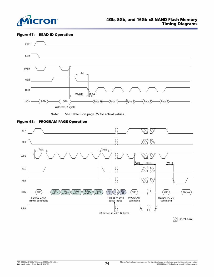
4Gb, 8Gb, and 16Gb x8 NAND Flash MemoryTiming Diagrams
Figure 67: READ ID Operation
Note: See Table 8 on page 25 for actual values.
Figure 68: PROGRAM PAGE Operation
WE#
CE#
ALE
CLE
RE#
I/Ox
Address, 1 cycle
90h 00h Byte 2Byte 0 Byte 1 Byte 3 Byte 4
tAR
tREAtWHR
WE#
CE#
ALE
CLE
RE#
R/B#
I/Ox
tWC tADL
SERIAL DATAINPUT command
x8 device: m = 2,112 bytes
PROGRAMcommand
READ STATUScommand
1 up to m Byteserial input
80h Coladd 1
Coladd 2
Rowadd 1
Rowadd 2
Rowadd 3
DINN
DINM 70h Status10h
tPROG tWHRtWB
Don’t Care
PDF: 09005aef81b80e13/Source: 09005aef81b80eac Micron Technology, Inc., reserves the right to change products or specifications without notice.4gb_nand_m40a__2.fm - Rev. B 2/07 EN 74 ©2006 Micron Technology, Inc. All rights reserved.
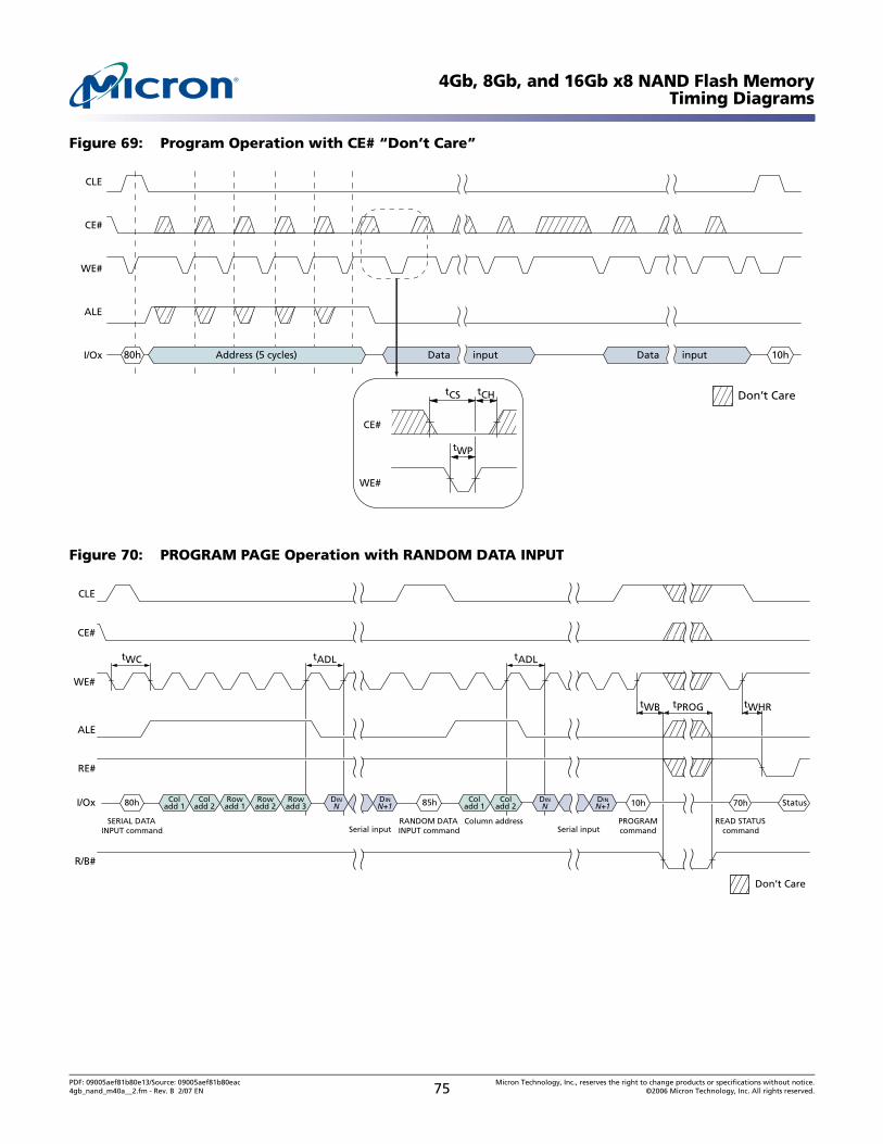
4Gb, 8Gb, and 16Gb x8 NAND Flash MemoryTiming Diagrams
Figure 69: Program Operation with CE# “Don’t Care”
Figure 70: PROGRAM PAGE Operation with RANDOM DATA INPUT
CLE
CE#
WE#
ALE
I/Ox Address (5 cycles) Data input 10h
WE#
CE#
tWP
tCHtCS Don’t Care
Data input80h
WE#
CE#
ALE
CLE
RE#
R/B#
I/Ox
tWC
SERIAL DATAINPUT command Serial input
80h Coladd 1
Coladd 2
Rowadd 1
Rowadd 2
Rowadd 3
DINN
DINN+1
tADL tADL
RANDOM DATAINPUT command
Column address PROGRAMcommand
READ STATUScommandSerial input
85h
tPROGtWB tWHR
Don’t Care
Coladd 1
Coladd 2
DINN
DINN+1 70h Status10h
PDF: 09005aef81b80e13/Source: 09005aef81b80eac Micron Technology, Inc., reserves the right to change products or specifications without notice.4gb_nand_m40a__2.fm - Rev. B 2/07 EN 75 ©2006 Micron Technology, Inc. All rights reserved.
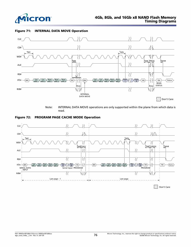
4Gb, 8Gb, and 16Gb x8 NAND Flash MemoryTiming Diagrams
Figure 71: INTERNAL DATA MOVE Operation
Note: INTERNAL DATA MOVE operations are only supported within the plane from which data is read.
Figure 72: PROGRAM PAGE CACHE MODE Operation
WE#
CE#
ALE
CLE
RE#
R/B#
I/Ox
tWB tPROGtWB
Busy BusyREAD
STATUS
tWC
INTERNALDATA MOVE
Don’t Care
tADL
tWHR
Coladd 2
Rowadd 1
Rowadd 2 70h10h StatusData
NRowadd 3
Coladd 100h 35hCol
add 2Row
add 1Row
add 2Row
add 3Col
add 185h Data1
tR
WE#
CE#
ALE
CLE
RE#
R/B#
I/Ox 15h
tCBSYtWB tWB tWHRtLPROG
Coladd 180h 10h 70h StatusCol
add 2Rowadd 2
Rowadd 1
Coladd 1
Coladd 2
Rowadd 2
Rowadd 1
Rowadd 3
DINM
DINN
DINM
DINN
Last page - 1 Last page
Serial input
tWC
Don’t Care
80h
tADL
Rowadd 3
SERIAL DATAINPUT
PROGRAM PROGRAM
PDF: 09005aef81b80e13/Source: 09005aef81b80eac Micron Technology, Inc., reserves the right to change products or specifications without notice.4gb_nand_m40a__2.fm - Rev. B 2/07 EN 76 ©2006 Micron Technology, Inc. All rights reserved.
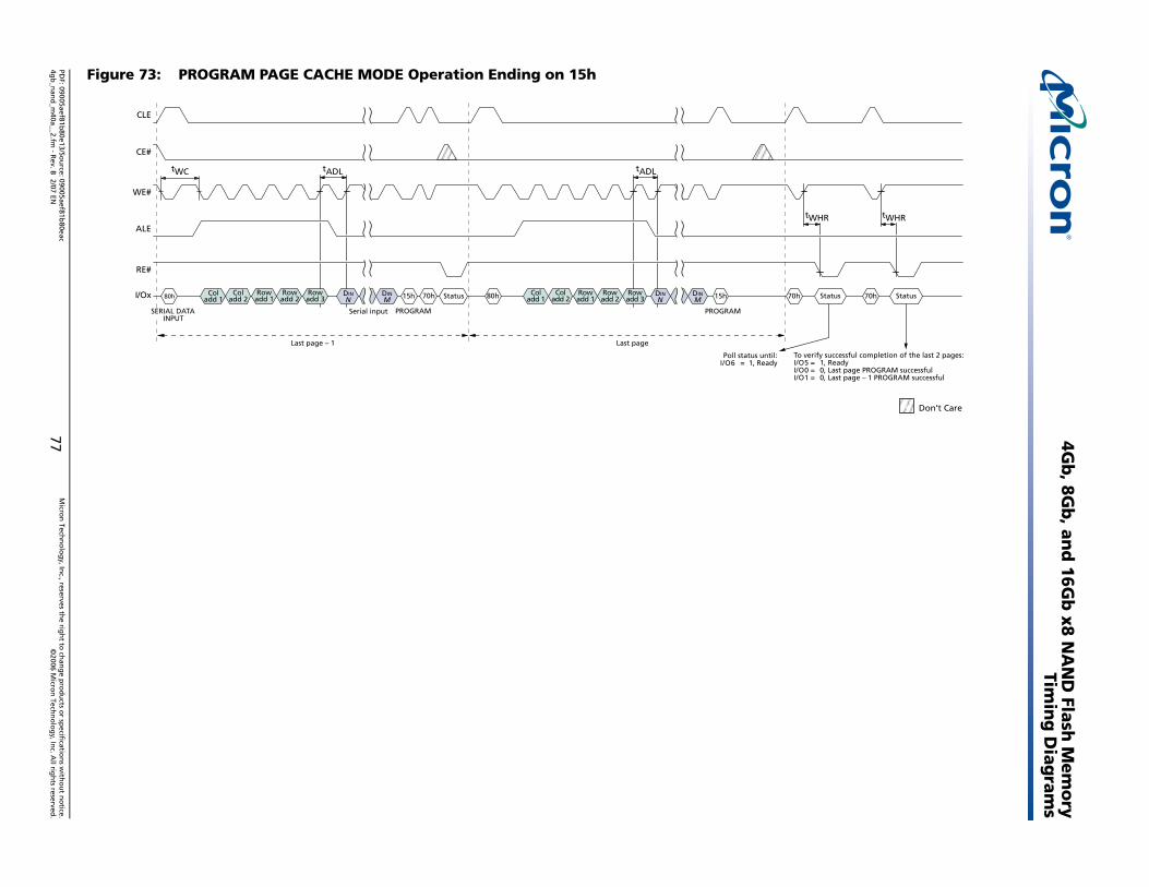
PDF: 09005aef81b
4gb
_nan
d_m
40a__2.fm-
Rev. B
2/07 EN77
©2006 M
icron
Techn
olo
gy, In
c. All rig
hts reserved
.
4Gb
, 8Gb
, and
16Gb
x8 NA
ND
Flash M
emo
ryTim
ing
Diag
rams
Figure 73: PROGRAM PAGE CACHE MODE Operation Ending on 15h
CLE
us 70h Status
Don’t Care
ccessful completion of the last 2 pages:eadyst page PROGRAM successful st page – 1 PROGRAM successful
tWHR
80e13/Sou
rce: 09005aef81b80eac
Micro
n Tech
no
log
y, Inc., reserves th
e righ
t to ch
ang
e pro
du
cts or sp
ecification
s with
ou
t no
tice.
WE#
CE#
ALE
RE#
I/Ox 15h Coladd 180h 15h 70h Stat70h Status Col
add 2Rowadd 2
Rowadd 1
Rowadd 3
Coladd 1
Coladd 2
Rowadd 2
Rowadd 1
Rowadd 3
DINM
DINN
DINM
DINN
Last pageLast page – 1
SERIAL DATAINPUT
Serial input PROGRAM PROGRAM
tWC
80h
Poll status until:I/O6 = 1, Ready
To verify suI/O5 = 1, RI/O0 = 0, LaI/O1 = 0, La
tADL
tWHR
tADL
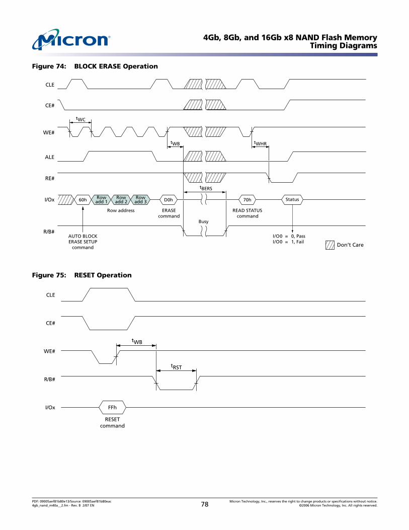
4Gb, 8Gb, and 16Gb x8 NAND Flash MemoryTiming Diagrams
Figure 74: BLOCK ERASE Operation
Figure 75: RESET Operation
WE#
CE#
ALE
CLE
RE#
R/B#
I/Ox
AUTO BLOCKERASE SETUP
command
ERASEcommand
READ STATUScommand
Busy
Row address
60h Rowadd 1
Rowadd 2
Rowadd 3 70h StatusD0h
tWC
tBERS
tWB tWHR
Don’t Care
I/O0 = 0, PassI/O0 = 1, Fail
CLE
CE#
WE#
R/B#
I/Ox
tRST
tWB
FFh
RESETcommand
PDF: 09005aef81b80e13/Source: 09005aef81b80eac Micron Technology, Inc., reserves the right to change products or specifications without notice.4gb_nand_m40a__2.fm - Rev. B 2/07 EN 78 ©2006 Micron Technology, Inc. All rights reserved.
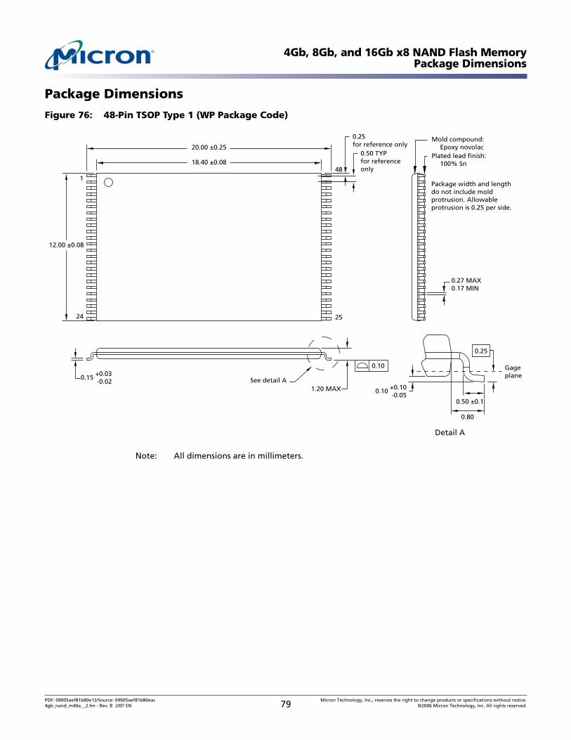
4Gb, 8Gb, and 16Gb x8 NAND Flash MemoryPackage Dimensions
Package Dimensions
Figure 76: 48-Pin TSOP Type 1 (WP Package Code)
Note: All dimensions are in millimeters.
1.20 MAX
0.15 +0.03 -0.02
0.27 MAX0.17 MIN
See detail A
18.40 ±0.08
20.00 ±0.25
Detail A
0.50 ±0.1
0.80
0.10 +0.10-0.05
0.10
0.25
Gageplane
0.25for reference only
0.50 TYPfor referenceonly
12.00 ±0.08
1
24
48
25
Plated lead finish: 100% Sn
Mold compound: Epoxy novolac
Package width and lengthdo not include moldprotrusion. Allowable protrusion is 0.25 per side.
PDF: 09005aef81b80e13/Source: 09005aef81b80eac Micron Technology, Inc., reserves the right to change products or specifications without notice.4gb_nand_m40a__2.fm - Rev. B 2/07 EN 79 ©2006 Micron Technology, Inc. All rights reserved.
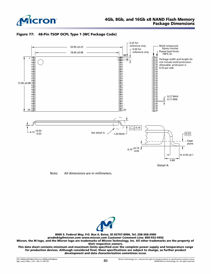
4Gb, 8Gb, and 16Gb x8 NAND Flash MemoryPackage Dimensions
Figure 77: 48-Pin TSOP OCPL Type 1 (WC Package Code)
Note: All dimensions are in millimeters.
1.20 MAX0.15 +0.03
-0.02
0.27 MAX0.17 MIN
See detail A
18.40 ±0.08
20.00 ±0.25
12.00 ±0.08
Detail A
0.50 ±0.1
0.80
0.10 +0.10-0.05
0.10
0.25
Gageplane
0.25 forreference only
0.50 forreference only
1
24
48
25
Plated lead finish: 100% Sn
Mold compound: Epoxy novolac
Package width and length donot include mold protrusion.Allowable protrusion is0.25 per side.
®
8000 S. Federal Way, P.O. Box 6, Boise, ID 83707-0006, Tel: [email protected] www.micron.com Customer Comment Line: 800-932-4992
Micron, the M logo, and the Micron logo are trademarks of Micron Technology, Inc. All other trademarks are the property of their respective owners.
This data sheet contains minimum and maximum limits specified over the complete power supply and temperature range for production devices. Although considered final, these specifications are subject to change, as further product
development and data characterization sometimes occur.
PDF: 09005aef81b80e13/Source: 09005aef81b80eac Micron Technology, Inc., reserves the right to change products or specifications without notice.4gb_nand_m40a__2.fm - Rev. B 2/07 EN 80 ©2006 Micron Technology, Inc. All rights reserved.
4Gb, 8Gb, and 16Gb x8 NAND Flash MemoryRevision History
Revision History
Rev. B . . . . . . . . . . . . . . . . . . . . . . . . . . . . . . . . . . . . . . . . . . . . . . . . . . . . . . . . . . . . . . . . . . . . . . . . . . . . . . . . . . . . . . . . . . . . . . . 2/07• Page 1: Added MT29F8G08BAA to title, 8Gb (dual-die stack 1 CE#), 8Gb (dual-die
stack 2 CE#) to density options, 2 die, 1 CE#, 1 RB# to configuration options. Added extended temperature to options.
• Figure 2 on page 2: Added classification B: 2 die, 1 CE#, 1 RB#. Added extended temperature and note to contact factory.
• “General Description” on page 8: Added MT29F8G08BAA to first paragraph; revised fourth paragraph.
• Figure 3 on page 9: Modified note 1.• Figure 5 on page 12: Revised block information.• Figure 7 on page 14: Added new part number information to figure title and note 2.• Table 4 on page 14: Changed part numbers in title.• Former Figure 8 on page 17, “Time Constants” and Figure 9 on page 17, “Minimum
Rp”: Converted to equation format.• Table 8 on page 25: Added MT29F8G08BAA in bytes 1, 2, and 4, modified interleaved
operations description, added note 3, changed part number in note 2.• “Two-Plane Addressing” on page 35: Revised second bullet re BA18.• “Error Management” on page 58: Modified second bullet.• Table 12 on page 59: Added extended temperature.• Tables 13 and 14 on page 61, Table 15 on page 62: Added MT29F8G08DAA.• Table 19 on page 64: Changed tCBSY (MAX) and tPROG (MAX) to 600µs.
Rev. A . . . . . . . . . . . . . . . . . . . . . . . . . . . . . . . . . . . . . . . . . . . . . . . . . . . . . . . . . . . . . . . . . . . . . . . . . . . . . . . . . . . . . . . . . . . . . . . 8/06• Initial release.
PDF: 09005aef81b80e13/Source: 09005aef81b80eac Micron Technology, Inc., reserves the right to change products or specifications without notice.4gb_nand_m40a__2.fm - Rev. B 2/07 EN 81 ©2006 Micron Technology, Inc. All rights reserved.