n o i Khomp Platform I g n I w - UFSC · S o f t w a r e / H a r d w a r e I n t e g r a t i o n...
30
Software/Hardware Integration October 2002 http://www.lisha.ufsc.br 1 Khomp Platform I PowerPC 405 GP LISHA/UFSC Marcelo Trierveiler Pereira Prof. Dr. Antônio Augusto Fröhlich {trier|guto}@lisha.ufsc.br http://www.lisha.ufsc.br/~{trier|guto} October 2002
-
Upload
nguyenhanh -
Category
Documents
-
view
214 -
download
0
Transcript of n o i Khomp Platform I g n I w - UFSC · S o f t w a r e / H a r d w a r e I n t e g r a t i o n...

Sof
twar
e/H
ard
war
e In
tegr
atio
n
October 2002 http://www.lisha.ufsc.br 1
Khomp Platform IPowerPC 405 GP
LISHA/UFSCMarcelo Trierveiler Pereira
Prof. Dr. Antônio Augusto Fröhlich{trier|guto}@lisha.ufsc.br
http://www.lisha.ufsc.br/~{trier|guto}
October 2002

Sof
twar
e/H
ard
war
e In
tegr
atio
n
October 2002 http://www.lisha.ufsc.br 2
Outline
� The Khomp Platform I
�
Overview
�
Layout
� The PowerPC Processor
�
Overview
�
Registers, I/O Control, Instruction Set
� Compiler
�
PPC Cross-Compiler
� Operating System Functions
�
Context Switch
�
Interrupts

Sof
twar
e/H
ard
war
e In
tegr
atio
n
October 2002 http://www.lisha.ufsc.br 3
The Khomp Platform I
� Historic
�
Developed by Khomp
�
Design house and hardware solution provider
�
Telecommunication embedded system
� Goals
�
Integration of telephone and network systems
�
Technologies
�
Telephone: E+M, R2D�
Network: Ethernet, Wireless, ATM
� Main design decisions
�
PowerPC embedded processor (programmability)
�
AD digital signal processor (voice appliances)

Sof
twar
e/H
ard
war
e In
tegr
atio
n
October 2002 http://www.lisha.ufsc.br 4
Khomp PI Overview
analogic signal
PPC 405GP
PLB
SDRAM Flash
FPGA
ADSP 2186N
Ethernet
Voice coprocessor
PCI
frames

Sof
twar
e/H
ard
war
e In
tegr
atio
n
October 2002 http://www.lisha.ufsc.br 5
Khomp Pl Layout
� � �� �� � �
��
��
��� �
��� �
� ��
�� � � �
�� � � �� � �� � � � ��� � � � �� �� � ! � " � # # $
� &%' (*) + � � �� � � �, ".- � /
0�12
0�12
� � � � �� �� �
� � � � �� �� �

Sof
twar
e/H
ard
war
e In
tegr
atio
n
October 2002 http://www.lisha.ufsc.br 6
Embedded PowerPC
� Historic
�
PowerPC was jointly developed by
�
IBM�
Motorola�
Apple Computer
�
Based on POWER architecture from RS/6000
� Main characteristics
�
Flexible configuration
�
Offers different price and performance

Sof
twar
e/H
ard
war
e In
tegr
atio
n
October 2002 http://www.lisha.ufsc.br 7
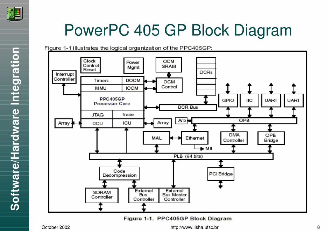
Power PC 405 GP Overview
� System on a chip (SoC) with RISC processor
� Cache
3
16 KB instruction cache / 8 KB data cache
� Timers
3
Programmable Interval Timer (PIT)
3
Fixed Interval Timer (FIT)
3
Watchdog Timer
� Paging-capable MMU
� 4 KB on-chip RAM
� Device Control Register Bus (DRC)
3
Peripheral control and status
Sof
twar
e/H
ard
war
e In
tegr
atio
n
October 2002 http://www.lisha.ufsc.br 8
PowerPC 405 GP Block Diagram

Sof
twar
e/H
ard
war
e In
tegr
atio
n
October 2002 http://www.lisha.ufsc.br 9
PowerPC 405 Data Types
� Data types
�
Bytes (8 bits)
�
Halfwords (16 bits)
�
Words (32 bits)
�
Strings (1 to 128 bytes)
� Instructions are always word-aligned
� Configurable byte ordering
�
Big-endian
�
Litlle-endian
MSB LSB
31 0
LSB MSB
31 0
Sof
twar
e/H
ard
war
e In
tegr
atio
n
October 2002 http://www.lisha.ufsc.br 10
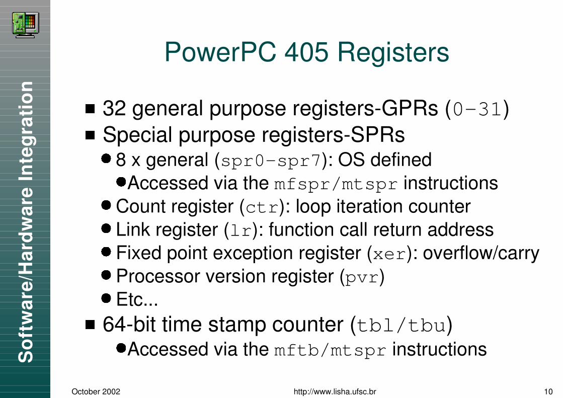
PowerPC 405 Registers
4 32 general purpose registers-GPRs (0-31)
4 Special purpose registers-SPRs
5
8 x general (spr0-spr7): OS defined
5
Accessed via the mfspr/mtspr instructions
5
Count register (ctr): loop iteration counter
5
Link register (lr): function call return address
5
Fixed point exception register (xer): overflow/carry
5
Processor version register (pvr)
5
Etc...
4 64-bit time stamp counter (tbl/tbu)
5
Accessed via the mftb/mtspr instructions

Sof
twar
e/H
ard
war
e In
tegr
atio
n
October 2002 http://www.lisha.ufsc.br 11
PowerPC 405 Registers
4 Machine status register (msr)
5
Controls interrupts, debugging, etc
5
Accessed via the mfmsr/mtmsr instructions
4 8 x condition registers (cr0-cr7)
5
4-bits: LT(0), GT(1), EQ(2), SO(3)
4 Device control registers (dcr)
5
Accessed via the mfdcr/mtdcr instructions
4 Interrupt context registers (ssr0-ssr3)
6
Non-critical interrupts: ssr0 <- pc, ssr1 <- msr
6
Critical interrupts: ssr2 <- pc, ssr3 <- msr

Sof
twar
e/H
ard
war
e In
tegr
atio
n
October 2002 http://www.lisha.ufsc.br 12
PowerPC 405 Instruction Set
7 Storage: lwz,stw, etc.
7 Arithmetic: add, subf, neg, mullw (4-cicle), divw (35-cicle), etc
7 Logical: and, or, xor, not, etc
7 Comparison: cmp, etc
7 Branch: b, bc (conditional), bclr (link register), etc
7 Condition register logical: crand, cror, etc
7 Shift and rotate: slw (shift left word), rotlw (rotate left word), etc

Sof
twar
e/H
ard
war
e In
tegr
atio
n
October 2002 http://www.lisha.ufsc.br 13
PowerPC 405 Instruction Set
4 Cache management: dcbi/icbi (invalidate), dcbf (flush), icread/dcread (read)
4 Interruptions
5
Enable/disable: mtmsr, mfmsr
5
Return: rfci, rfi
4 Process management
5
System call: sc
4 Example: jumpb[l][a] <addr>
b = branch: PC = PC + <addr>l = link register: LR = PCa = absolute: PC = <addr><addr> = signed address: 26 bits (+/- 32 MB)

Sof
twar
e/H
ard
war
e In
tegr
atio
n
October 2002 http://www.lisha.ufsc.br 14
PowerPC 405 Memory Management
4 Memory Management Unit (MMU)
5
Implements paging
8
Variable page size (1K - 16M)8
Per-page protection and storage attributes
5
Translation Lookaside Buffer (TLB)
8
64 entries (40 bits log -> 32 bits phy)8
Logical addresses are associated with pid[24:31] register8
TLB miss triggers interrupts (software management)
5
Controlled via msr[ir,dr]
8
Enable/disable for data/instructions8
Implicitly disabled during interrupts

Sof
twar
e/H
ard
war
e In
tegr
atio
n
October 2002 http://www.lisha.ufsc.br 15
PowerPC 405 Memory Management

Sof
twar
e/H
ard
war
e In
tegr
atio
n
October 2002 http://www.lisha.ufsc.br 16
PowerPC 405 I/O
9 Device control registers (dcr)
:
Defined outside the processor core
:
Control on-chip peripherals and busses
:
Can define an I/O address space or directly map device registers
:
Accessed via the mfdcr/mtdcr instructions
9 Memory mapped I/O (mmio)
;
I/O address space interwoven in the global address space
Sof
twar
e/H
ard
war
e In
tegr
atio
n
October 2002 http://www.lisha.ufsc.br 17
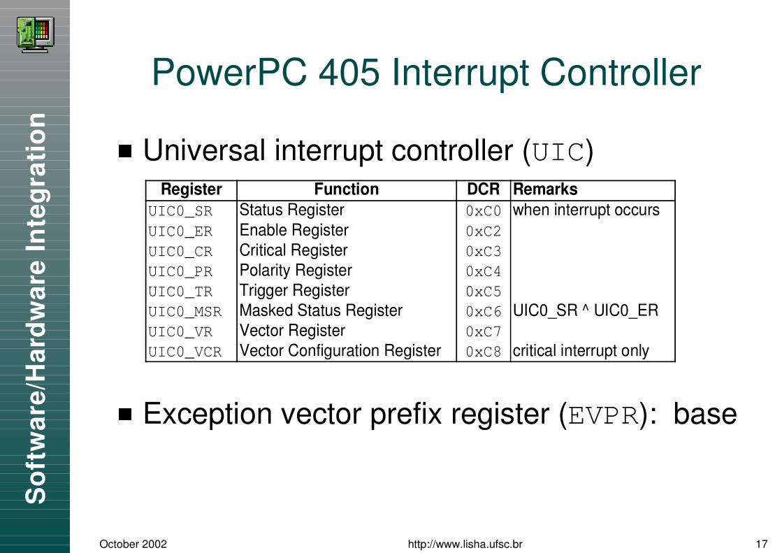
PowerPC 405 Interrupt Controller
7 Universal interrupt controller (UIC)
7 Exception vector prefix register (EVPR): base
Register Function DCR RemarksUIC0_SR Status Register 0xC0 when interrupt occursUIC0_ER Enable Register 0xC2UIC0_CR Critical Register 0xC3UIC0_PR Polarity Register 0xC4UIC0_TR Trigger Register 0xC5UIC0_MSR Masked Status Register 0xC6 UIC0_SR ^ UIC0_ERUIC0_VR Vector Register 0xC7UIC0_VCR Vector Configuration Register 0xC8 critical interrupt only

Sof
twar
e/H
ard
war
e In
tegr
atio
n
October 2002 http://www.lisha.ufsc.br 18
PowerPC 405 Interrupt Handling
9 32 configurable interrupts
:
Non-critical interrupts
8
Handled via special vector registers (offset at 0x0500)srr0 <- pcsrr1 <- msrmsr <- msr & ~intpc <- 0x0500 + EVPR[16:32]
<
Critical interrupts
=
Handled via special vector registers (offset at 0x0100)srr2 <- pcsrr3 <- msrmsr <- msr & ~intpc <- 0x0100 + EVPR[16:32]UIC0_VR <- (512*int_no) + UIC0_VCR

Sof
twar
e/H
ard
war
e In
tegr
atio
n
October 2002 http://www.lisha.ufsc.br 19
PowerPC 405 Initialization
9 After reset
:
PC contains 0xfffffffc
8
Room for a branch into the actual initialization firmware
:
MMU, IC, on-chip devices are disabled
:
MSR and DCR contains 0x00000000
8
Except EBC0_SLOT0 (boot configuration)
9 Initialization firmware
:
Stored in non-volatile memory
8
Attached to EBC[0] or PCI
:
Configures a 'basic' environment
8
On-chip memory, Interrupt controller, External bus, etc
:
Copy OS code to RAM and jump
Sof
twar
e/H
ard
war
e In
tegr
atio
n
October 2002 http://www.lisha.ufsc.br 20
PowerPC 405Operating System Integration
> Initialization
> Interrupt handling
> I/O handling
> Memory management
> Context switch

Sof
twar
e/H
ard
war
e In
tegr
atio
n
October 2002 http://www.lisha.ufsc.br 21
Initialization
9 Succeeds the initialization procedure in firmware
9 Main tasks
:
Activate the MMU
:
Activate the Cache
:
Activate timers
:
Scan buses for devices
:
Reconfigure interrupts
:
Loads the OS
:
Creates the first application process

Sof
twar
e/H
ard
war
e In
tegr
atio
n
October 2002 http://www.lisha.ufsc.br 22
Interrupt Handling
> Critical interrupt example:
srr2 <- pc;srr3 <- msr;msr <- msr & ~int;UIC0_VR <- UIC0_VCR + (512*int_no);pc <- 0x0100 + EVPR[16:32];
0x100:mfdcr r0, 0x0c7; //Vector Registerb r0;

Sof
twar
e/H
ard
war
e In
tegr
atio
n
October 2002 http://www.lisha.ufsc.br 23
I/O Handling (MMIO)
? Example: UART
@
Transmitter Holding Register is MMIO at 0xef600300
@
Sending a byte through the serial port
char * UART_THR = (char *)0xef600300;UART_THR = 0xaa;

Sof
twar
e/H
ard
war
e In
tegr
atio
n
October 2002 http://www.lisha.ufsc.br 24
I/O Handling (DCR)
? Example: External Bus Controller (EBC)
@
EBC is formed by 8 slots
@
Configured by 2 DCRs:
A
EBC Config Address: EBC0_CFGADDR = 0x12A
EBC Config Data: EBC0_CFGDATA = 0x13
char DCR_Addr_Offset = 0x12;char DCR_Data_Offset = 0x13;char EBC_Config_Offset = 0x00; // Slot 0unsigned int Data = 0xaaaaaaaa;
mtdcr DCR_Addr_Offset, EBC_Config_Offset;mtdcr DCR_Data_Offset, Data;

Sof
twar
e/H
ard
war
e In
tegr
atio
n
October 2002 http://www.lisha.ufsc.br 25
Memory Management
? Process ID Register (pid)
@
Enables work-set preservation across processes
@
8 bits appended to TLB entries (log. addr.)
? On context switch
@
Invalidate TLB or
@
Change pid
? OS must handle
@
TLB misses
A
Page-table lookup, victim selection , replace
@
Page-faults
A
Demand paging (virtual memory)A
OS-specific treats (copy-on-write, stack grow, etc)

Sof
twar
e/H
ard
war
e In
tegr
atio
n
October 2002 http://www.lisha.ufsc.br 26
Context Switch Example
void context_switch(int **old_sp, int *new_sp){ // get old_sp asm("lwz r1, 0(r3) \n"
// save general registers "stwu r0,-4(r1) \n" : "stwu r31,-4(r1) \n"
// save special registers "mflr r11 \n" "stwu r11,-4(r1) \n" "mfmsr r11 \n" "stwu r11,-4(r1) \n" : "mfxer r11 \n" "stwu r11, -4(r1) \n"
// sync memory and pipeline "sync \n"
// update old_sp "stw r1,0(r3) \n"
// get new_sp "mr r1,r4 \n"
// load special registers "lwzu r11,4(r1) \n" "mtxer r11 \n" : "lwzu r11,4(r1) \n" "mtmsr r11 \n" "lwzu r11,4(r1) \n" "mtlr r11 \n"
// load general registers "lwzu r31,4(r1) \n" : "lwzu r0,4(r1) \n"
// sync memory and pipeline "sync \n"}
Sof
twar
e/H
ard
war
e In
tegr
atio
n
October 2002 http://www.lisha.ufsc.br 27
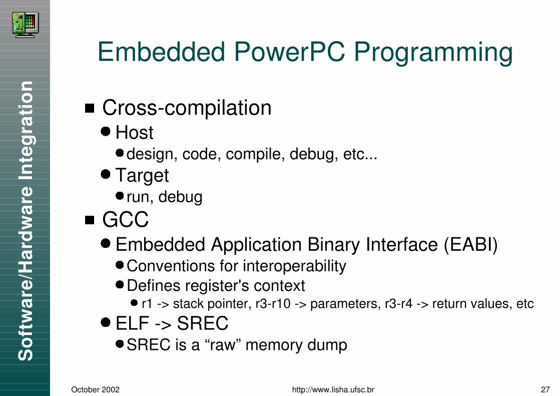
Embedded PowerPC Programming
? Cross-compilation
@
Host
A
design, code, compile, debug, etc...
@
Target
A
run, debug
? GCC
@
Embedded Application Binary Interface (EABI)
A
Conventions for interoperabilityA
Defines register's contextB
r1 -> stack pointer, r3-r10 -> parameters, r3-r4 -> return values, etc@
ELF -> SREC
A
SREC is a “raw” memory dump

Sof
twar
e/H
ard
war
e In
tegr
atio
n
October 2002 http://www.lisha.ufsc.br 28
PowerPC 405 RegistersAccess Control
Supervisor Model
User Model Storage Regs.Machine State Reg.
GPR[ 0 – 31 ] (r/w) Core Config. Reg.SPR 0 (r/w) SPRs[ 0 - 7 ]SPR[ 4 – 7 ] ( r ) Exception Regs.CR - Cond. Reg (r/w) Save/Restore Regs.XER - Fixed Point Reg. (r/w) Memory Manag. Regs.LR - Link Reg. (r/w) Processor Version Reg.CTR – Counter Reg. (r/w) Process Id. Reg.TBR – Timer Reg. ( r ) Debug Regs.
Timer Regs.External Core Regs.

Sof
twar
e/H
ard
war
e In
tegr
atio
n
October 2002 http://www.lisha.ufsc.br 29
PowerPC 405Device Control RegistersDevice Control Registers (DCRs)
SDRAM Memory ControllerEBC External Bus ControllerDCP Decompression ControllerOCM On-Chip MemoryPLB Processor Local BusOPB On-Chip Peripheral BusCPC Clock, Power Management, Chip ctl.UIC Universal Interrupt ControllerDMA Direct Memory Access ControllerMAL Memory Access LayerPCI Peripheral Component InterconnectUART Serial Port ControllerIIC Inter-Integrated CircuitGPIO General-Purpose I/O ControllerEMAC Ethernet Memory Access Controller

Sof
twar
e/H
ard
war
e In
tegr
atio
n
October 2002 http://www.lisha.ufsc.br 30
PowerPC 405Default Address Space
Function Start Addr. End Addr. SizeLocal Memory/ 0x0000 0000 0x7FFF FFFF 2GBPeripheralsPCI Space 0x8000 0000 0xEF5F FFFF 1.744GBInternal 0xEF60 0000 0xEFFF FFFF 10MBPeripheralsExpansion ROM 0xF000 0000 0xFFDF FFFF 454MBBoot ROM 0xFFE0 0000 0xFFFF FFFF 2MB