
N Inc. Lewis - Digital Library/67531/metadc676887/...phase epitaxy (OMVPE) reactor described...
15
I. InGaAs MONOLITHIC INTERCONNECTED MODULES (MIM) N avid S. Fatemi, Essential Research, Inc. David M. Wilt, NASA Lewis Research Center Philip P. Jenkins, Essentiaf Research, Inc. Victor G. Weizer, NASA Lewis Research Center Richard W. Hoffman, Jr., Essential Research lnc. David Scheimann, NASA Lewis Research Center Oavid Brinker, NASA Lewis Research Center Christopher S. Murray, Bettis Atomic Power Laboratory David R. Riley, 8ettis Atomic Power Laboratory DE-AC11-93PN38195 NOTtCE I mlr report was prepared IS an account of work sponsored by the Untted States Government Neithw tho UnHed Stater, nor the Unitod Stater Department of Energy, nor m y of their employees, nor any of th& contractorr, subcontractor$, 01 th4ir ompJoyees, maker my werrmty, rxpr.r, or Implied, or msumes any hat Ilabiiity or rerponrlbiiity for thr .ccurrcy, Completenew Q? utefulnou of any Informatbn, apparatus, product 01 prows8 disclosed, or reprrs.4nts that Itr UH would not InfrIng. prfvatoly owned rights. BRTIS ATOMIC POWER LABORATORY WEST MIFFLIN, PENNSYLVANIA 15122-0079 Operated for the US. Department of Energy by WESTtNGHOUSE ELECTRIC CORPORATION
Transcript of N Inc. Lewis - Digital Library/67531/metadc676887/...phase epitaxy (OMVPE) reactor described...
I .
InGaAs MONOLITHIC INTERCONNECTED MODULES (MIM)
N avid S. Fatemi, Essential Research, Inc. David M. Wilt, NASA Lewis Research Center Philip P. Jenkins, Essentiaf Research, Inc.
Victor G. Weizer, NASA Lewis Research Center Richard W. Hoffman, Jr., Essential Research lnc. David Scheimann, NASA Lewis Research Center
Oavid Brinker, NASA Lewis Research Center Christopher S. Murray, Bettis Atomic Power Laboratory
David R. Riley, 8ettis Atomic Power Laboratory
DE-AC11-93PN38195
NOTtCE I mlr report was prepared IS an account of work sponsored by the Untted States Government Neithw tho UnHed Stater, nor the Unitod Stater Department of Energy, nor m y of their employees, nor any of th& contractorr, subcontractor$, 01 th4ir ompJoyees, maker my werrmty, rxpr.r, or Implied, or msumes any h a t Ilabiiity or rerponrlbiiity for thr .ccurrcy, Completenew Q? utefulnou of any Informatbn, apparatus, product 01 prows8 disclosed, or reprrs.4nts that Itr UH would not InfrIng. prfvatoly owned rights.
BRTIS ATOMIC POWER LABORATORY WEST MIFFLIN, PENNSYLVANIA 15122-0079
Operated for the US. Department of Energy by WESTtNGHOUSE ELECTRIC CORPORATION
InGaAs MONOLITHIC INTERCONNECTED MODULES (MIM)
Navid S. Fatemi', David M. Wilt', Phillip P. Jenkins', Victor G. yirer', Richard W. Hoffman, k.', Christopher S. Murray', David Riley', David Scheiman , and David Brinkerr,
Essential Research, Inc., Cleveland, OH. NASA Lewis Research Center, Cleveland, OH,
Westinghouse Electric Corporation, West Mimin, PA
1
2 3
ABSTRACT
A monolithic interconnected module (MIM) structure has been developed for thermophotovoltaic (TPV) applications. The MIM device consists of many individual InGaAs cells series-connected on a single semi-insulating (S.I.) InP substrate. An infrared (IR) back surface reflector (BSR), placed on the rear surface of the substrate, returns the unused portion of the TPV radiator output spectrum back to the emitter for recycling, thereby providing for hi& system efficiencies. Also, the use of a BSR obviates the need to use a separate filtering element, As a result, MIMs are exposed to the entire emitter output, thereby maximizing output power density. MIMs with an active area of lxl-cm were comprised of 15 cells monolithically connected in series. Both lattice-matched and lattice-mismatched InGaAs/InP devices were produced, with bandgaps of 0.74 and 0.55 eV, respectively. The 0.74-eV modules demonstrated an open-circuit voltage (Voc) of 6. I58 V and a fill factor of 74.2% at a short-circuit current (Jsc) of 842 mA/cm*, under flashlamp testing. The 0.55-eV modules demonstrated a Voc of 4.849 V and a fill factor of 57.8% at a Jsc of 3.87 Afcm2. IR reflectance measurements (Le., h > 2 pm) of these devices indicated a reflectivity of 1 83%. Latest electrical and optical performance results for our MIMs will be presented.
INTRODUCTION
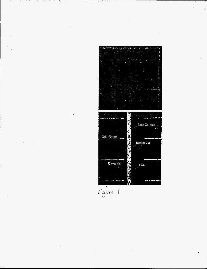
Most thermophotovoltaic (TPV) systems currently under consideration envision utilizing planar, one-junction low-bandgap (Eg) photovoltaic (PV) cells, such as InGaAs/InP, GaSb, and InGaS bAs/GaSb.l" Under their operating conditions, these devices commonly exhibit current densities in the range of 1-10 Ncm2, and voltages in the range of 400-550 mV. In a TPV system, however, these cells are connected in series to create a high-voltageflowcurrent configuration: to provide a usable external bus voltage, and to keep 12R resistive power losses to acceptable levels. Another approach to achieving a high-voltagellow-cunent configuration is to fabricate a device, where smalI area PV cells are connected in series monolithicdly. This results in the formation of a single high-voltageflow-cunent module. We have termed such a device, a monolithic interconnected module (MIM). Planar views of a MIM device are shown in Figure. 1.
eficiently recycle the incoming non-convertible infiared (IR) radiation. As shown in Figure 1, the fabrication of MIM requires the use of a semi-insulating (S.I.) InP substrate. S.1. InP is
. transparent to infrared (IR) radiation. Radiation with wavelengths (h) greater than the device bandedge wavelength (Le., h 2 -2 pin) can be reflected back to the TPV radiator via a back
Another important advantage of a MIM, compared to a conventional PV cell, is its ability to
-

DISCLAIMER
This report was prepared as an account of work sponsored by an agency of the United States Government. Neither the United States Government nor any agency thereof, nor any of their employees, makes any warranty, express or implied, or assumes any legal liability or responsibility for the accuracy, completeness, or use- fulness of any information, apparatus, product, or process disclosed, or represents that its use would not infringe privately owned rights. Reference herein to any spe- cific commercial product, process, or service by trade name, trademark, manufac- turer. or otherwise does not necessarily constitute or imply its endorsement, recom- mendation. or favoring by the United States Government or any agency thereof. The views and opinions of authors expressed herein do not necessarily state or reflect those of the United States Government or any agency thereof.

DISCLAIMER
Portions of this document may be illegible in electronic image products. Images are produced from the best available original document.
surface reflector (BSR). The BSR also provides for the convertible in-band radiation to get a second pass through the active regions of the device, increasing the effective cell collection e f i ~ i e n c y . ~
Figure I.-Planar view of a MIM (top), and close-up view of an interconnect area (bottom).
There are other advantages to a MIM design. Since both the negative and positive electrical connections are made to the top side of the module, array design, fabrication, and thermai management are simplified. The completed device may be soldered directly onto the array substrateheat sink without having to provide electrical isolation. Finally, the rear surface IR reflector eliminates the need for a separate filtering element. Without a filter, and its inherent transmission and re-radiation losses, the system design is simplified and the power density is increased.
MIMs, grown by organo-metallic vapor phase epitaxy (OMVPE). These structures had bandgaps of 0.74 and 0.55 eV, respectively. In what follows, we will discuss the design and fabrication of our MIMs, and present data regarding their electrical and optical performance.
We have fabricated and tested both lattice-matched and Iattice-mismatched p/n InGaAsArP
Device Design and Fabrication
The MIM structures were deposited in a horizontal, low-pressure organo-metallicvapor phase epitaxy (OMVPE) reactor described elsewhere6 The precursor materials were trimethyl indium (TMIn), trimethyl gallium(TMGa), arsine, phosphine, diethyl zinc (DEZn), and silane for p-and n-type doping, respectively. Conventional Au-Ge' and the more adherent Cr-Aus contact metallizations were deposited on the emitter and the lateral conduction layer (i.e., back contact) of the device simultaneously. A dielectric barrier layer, deposited by electron-beam evaporated Ta205, was used to prevent the interconnect metallization from shorting out the individual cells.
In our past works on MI&, we had designed and fabricated lxl-cm modules that had eight (8) series-connected cells? The devices presented in this work are, however, composed of fifteen (1 5 ) p/n InGaAs cells monolithically interconnected in series. By minimizingthe packing factor in the new 15-cell MIM design, we were able to actually reduce the total interconnect metal shadowing, relative to the older 8-cell MIM design. The packing factor for the 15-ceiI MIM device was 92%, but only slightly less than half of the interconnect area was optically opaque to the input radiation.
In every interconnect region, a trench via was etched down to the semi-insulating IRP substrate. This via served to electrically isolate one individual cell &om the adjacent cell. Near this via, another wider via was etched down to the lateral conduction layer, where the back contact metallization was later deposited. The interconnect region (or the packing factor) for the module is comprised of the trench via, the back contact metallization, and the interconnect
2
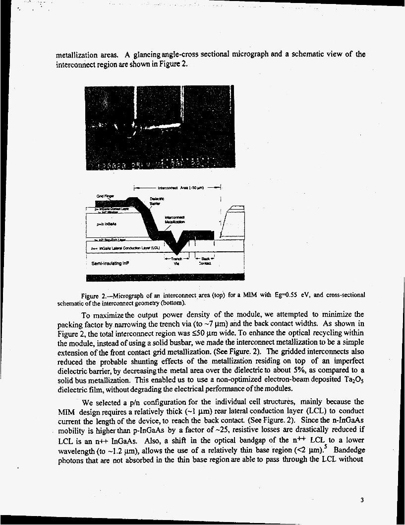
metallization areas. A glancingangle-cross sectional micrograph and a schematic view of the interconnect region are shown in Figure 2.
I m-
Figure 2.-Micrograph of an interconnect m a (top) for a MIM with Eg-0.55 eV, and cross-sectional schematic of the intercom-ect geometry (bottom).
To maximizethe output power density of the module, we attempted to minimize the packing factor by narrowing the trench via (to -7 p) and the back contact widths. As shown in Figure 2, the total interconnect region was S O pm wide. To enhance the optical recycling within the module, instead of using a solid busbar, we made the interconnect metallization to be a simple extension of the fiont contact grid metallization. (See Figure. 2). The gridded interconnects also reduced the probable shunting effects of the metallization residing on top of an imperfect dielectric barrier, by decreasingthe metal area over the dielectric to about 5%, as compared to a solid bus metallization. This enabled us to use a non-optimized electron-beam deposited Ta20s dielectric film, without degrading the electrical performance of the modules.
We selected a pln configuration for the individual cell structures, mainly because the MIM design requires a reIatively thick (-1 pn) rear lateral conduction layer (LCL) to conduct current the length of the device, to reach the back contact. (See Figure. 2). Since the n-InGaAs mobility is higher than p-InGaAs by a factor of -25, resistive losses are drastically reduced if LCL is an ni-t InGaAs. Also, a shift in the optical bandgap of the n* LCL to a lower wavelength (to -1.2 pm), allows the use of a relatively thin base region (4 pin).' Bandedge photons that are not absorbed in the thin base region are able to pass through the LCL without
3
being absorbed. These photons then reflect off the BSR and pass through the base region a second time.
It is also important to minimize the thickness of all the doped layers in the device structure. This is because thinner (and lower doped) layers exhibit less free-carrier absorption (FCA). Lowering FCA is crucial to enhancingthe optical recycling esciency of the MIM. We have also found that for comparably-doped layers of the same thickness, FCA was significantly lower for n- InGaAs, as compared to p-InGaAs?
Electrical and Optical Results
High-intensity illumination current versus voltage (1-9, quantum yield (QY), and reflectivity (R(h)) measurements were performed to characterize the MIMs. We present data for both lattice-matched and lattice-mismatched p/n 1nGaAdn.P structures, with bandgaps of 0.74 and 0.55 eV, respectively. As compared to our more optimized lattice-matched MIM structures, the data for the non-optimized lattice-mismatched devices are only preliminary.
Current-voltage (I- data Historically, nearly all the reports on the growth and characterization of low bandgap
InGaAs cells have been focused on the d p ~onfiguration.'-~ As a result, to verify the basic material quality, we fabricated base-line conventional planar p/n InGaAs cells (Eg4.74 eV), prior to fabricating MIM devices. These cells exhibited record efficiencies under air-mass zero (AMO) illumination conditions9 We then proceeded to grow, fabricate, and test the MIM devices.
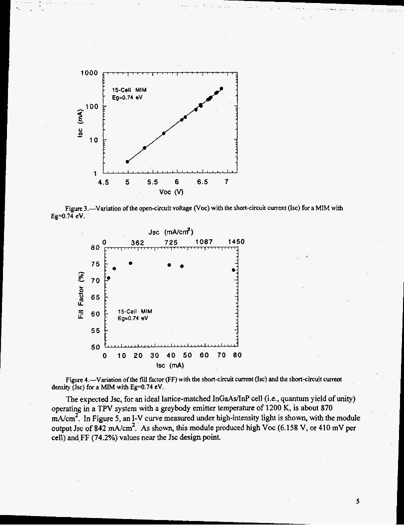
These MIM devices were tested under high-intensity illumination, using a large-area pulsed solar simulator (LAPS), to assess their performance under simulated operating conditions. The results for the variation in the open-circuit voltage (Voc) and fill factor (FF) with the short-circuit current (Isc), of a 1 5-cell MIM (Eg=0.74 eV) are given in Figures 3 and 4. As seen in the figures, the diode ideality factor (A) for the device was unity. Also, the FF values remained above 70% in the Isc range of interest. This result indicates that resistive losses are acceptably low in these devices at the anticipated operating TPV output current levels.
4

50 7
4 0 c C
30 3 20
10
0 0 1 2 3 4 5 6 7
Voltage (V)
Figure 5.Aurrent-voltage (I-V) characteristics of a MIM, with Eg=0.74 eV, measured under high-intensity
We also performed high-intensity illumination measurements on our non-optimized lattice- illumination.
mismatched MIMs (Eg4.55 eV). In Figures 6 and 7, data is presented for variations of Voc and FF as a function of Isc, respectively. The diode ideality factor for these device was only slightly above unity. The Voc values for these devices were, however, somewhat lower than the values we have obtained with our conventional planar cells in the past. The FF values, on the other hand, remained close to the 60% mark in the Isc range of interest.
Figure 6.-Variation of the open-circuit voItage (VOC) with the short-circuit current (Isc) for a MIM with Eg4.55 eV.
6

JSC (A/cm2) 0 0.90 I .a 2.7 3.6
0 0 e
5 2 ;
5 0 . . ' ' I . . . ' I ' ' ' , ' . ' ' ' 0 5 0 100 150 200
Isc (mA)
Figure 7.-Variation of the fiIl factor (FF) with the short-circuit current (1%) and the short-circuit current density (Jsc) for a MIM with Eg4.55 eV.
For a cell with Efl .55 eV (and a quantum yield of Unity), operating under a greybody emitter (T=1200 K), the expected Jsc is about 3.72 A/cm2. An I-V curve for a module with Jsc of 3.87 Ncm2 is shown Figure 8. The Voc and FF values were 4.849 V (323 mV per cell) and 57.8%, respectively.
2 5 0
2 0 0 a E Y 150 c
U c L 100 5
50
0
t ' " " ' " " " " ' ' " " ' " " ~ -
0 1 2 3 4 5 Voltage (V)
Figure &-Cunent-voltage (I-V) characteristics of a MIM, with Egg.55 eV, measured under high-intensity illumination.
Quantum yield (QU data The quantum yield (QY) data for our lattice-matched MMs ([email protected] ev) showed
extremely good collection efficiency. This data is given in Figure 9. Two external and one internal QY curves are shown in the figure. The external QY curves illustrate the effectiveness of the BSR in improving the current collection. As expected, the increase in current collection due
I 7
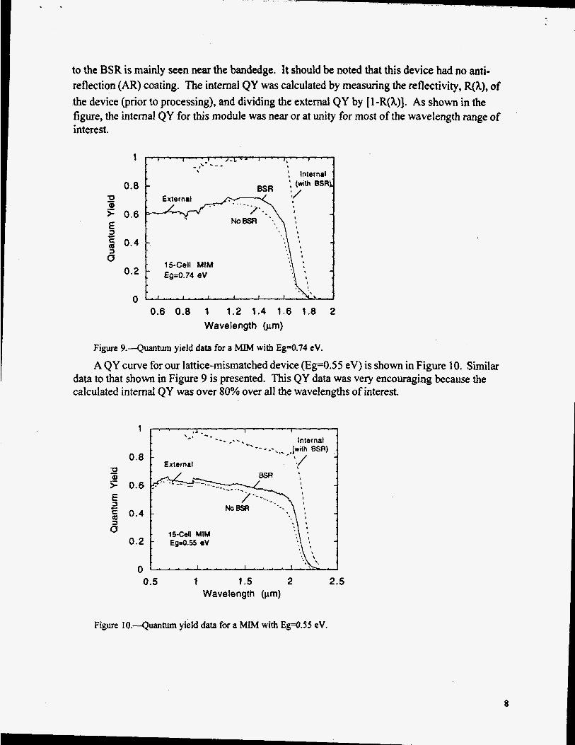
to the BSR is mainly seen near the bandedge. It shodd be noted that this device had no anti- reflection (AR) coating. The internal QY was calculated by measwing the reflectivity, R(Q, of the device (prior to processing), and dividing the external QY by [ 1-R(h)]. As shown in the figure, the internal QY for this module was near or at unity for most of the wavelength range of interest.
1
0.8
5 0.6 U 9) - E 2 0.4 3 - 6
0.2
0
- . External
-
- 15-Cell MIM . Eg=0.74 eV
0.6 0.8 1 1.2 1.4 1.6 1.8 2 Wavelength (pm)
Figure 9.--Quantum yield data for a MIM with Eg4.74 eV.
A QY curve for our lattice-mismatched device (Eg=0.55 eV) is shown in Figure 10. Similar data to that shown in Figure 9 is presented. This QY data was very encouraging because the calculated internal QY was over 80% over all the wavelengths of interest.
0 F a
E t c (II
c
6
1
0.8
0.6
0.4
0.2
0.5 1 1.5 2 2.5 Wavelength (pm)
Figure iO.--Quantum yield data for a MIM with Eg4.55 eV.
8

-i . . ,
I %
Reflectivity riata
To maximize optical recycling efficiency, the reflectivity of the MIMs (with a BSR), beyond the bandedge wavelength must be as high as possible. This allows for the majority of the non- convertible IR photons to ?x reflected back to the TPV emitter for recycling. Therefore, we performed reflectivity measurements of the modules with bandgaps of 0.74 and 0.55 eV, before they were processed into complete devices. Both structures had thick (-2 pm) gold BSRs. The results are shown in Figures 1 I and 12.
Figure 1 1.-Reflectivity data for a MIM structure, with Eg-0.74 eV, without anti-reflection coating.
Figure IZ.--Reflectivity data for a MIM structure, with Eg4.55 eV, without anti-reflection coating.
As seen in the figures, the out-of-band IR reflectivity (k > -2 pm) for these structures was 84 and 83% for bandgaps of 0.74 and 0.55 eV, respectively. The gold BSR IR reflectivity, as measured through a semi-insulating InP substrate, is greater than 95%. The somewhat lower reflectivities measured with the MIM structures were, therefore, due to the free-carrier
9
- .
absorption within the doped layers of the devices. By modifying the module design, we expect to increase this reflectivity to near 90%.
Summary
The results presented in this work are summarized below:
1. We fabricated and tested both lattice-matched and lattice-mismatched InGaAsfinP monolithic interconnected modules (MIM), with bandgaps of 0.74 and 0.55 eV, respectively. These devices had an active area of 1x1 cm and were comprised of 15 cells interconnected in series. They had a gold back surface reflector (BSR) layer to allow for efficient radiation recycling, when used in a TPV system.
2. MIM devices were tested under high-intensity illumination. The I-V results for the structures with a bandgap of 0.74 eV were: V0~6.158 V and fill factor=74.2% for Jsc=842 mA/cm2. The I-V results for the structures with a bandgap of 0.55 eV were: Voc4.849 V and fill facto1=57.8% for Jsc=3.87 A/cm2.
3. The internal quantum yield for the MIM devices were determined to be at or near unity for the module with Eg=0.74 eV, and over 80% for the module with Eg4.55 eV, over the wavelength range of interest.
4. The reflectivity as a hc t ion of wavelength for both lattice-matched and lattice- mismatched structures was measured to be 183% in the infrared (Le., h > -2pm) region of the spectrum.
References
1. D. M. Wilt, N. S. Fatemi, R.W. HoEnan, P. Jenkins, D. Brinker, D. Scheiman, & R. Jain, “High efficiency lnGaAs photovoltaic devices for thermophotovoltaic applications,” 64,241 5 (1994).
2. N. S. Fatemi, R.W. Hoffman, D. M. Wilt, R Lowe, P. Jenkins, L. M. Garvenck, and D. Scheiman, “High efficiency converters for thermophotovoltaic applications,” 3 1 st IECEC, Washington, D.C., August 1996.
3. SJ. Wojtczuk, “lnGaAs TPV experiment-based performance models,” 2nd NREL TPV Conf., Colorado Springs, CO, July 17-19, 1995, p. 387.
4. G.W. Charache, J.L. Egley, L.R. Danielson, D.M. Depoy, P.F. Baldasam, B.C. Campbell, S. Hui, L.M. Fraas, and S.J. WojtcNk, “Current status of low-temperature radiator TPV devices,” 25th IEEE PVSC, May 13- 17, 1996, Washington, DC, p.137.
5. D. M. Wilt, N. S. Fatemi, P.P. Jenkins, V.G. Weizer, R.W. Hof&nan, C.S. Murray, and D. Riley, “EIectrical and optical performance characteristics of pln InGaAs monolithic interconnected modules,” 32nd IECEC, HI, August 1997.

6. D. M. Wilt, N. S. Fatemi, P. P. Jenkins, R.W. Hofhan, G.A. Landis, and R.K. Jain, “Monolithically interconnected InGaAs TPV module development,” 26th PVSC, Washington, DC, May 13-17, 1996, p. 43.
7. N. S. Faremi, V. G. Weizer, D. M. Wilt, and R. W. Hoffman, “Ultra-low mistance, non-destructive contact system for InPAnGaAsAnP double heterostmcture TPV devices” 26th PVSC. Washington, DC, May 13-17, 1996, p. 85.
8. N. S. Fatemi, D. M. Wilt, P.P. Jenkins, R.W. Hof6nan, V.G. Weizer, C.S. Murray, and D. Riley, “Materials and process development for the monolithic interconnected module (MIM) InGaAdnP TPV devices,” 3rd N M L TPV Conf., Colorado Springs, CO, May 18-21, 1997.
“Elecmcal and optical performance characteristics of p/n 0.74-eV InGaAs monolithic interconnected modules,” 3rd NREL TPV Conf., Colorado Springs, CO, May 18-21, 1997.
9. D. M. Wilt, N. S. Fatemi, P.P. Jenkins, V.G. Weizer, R.W. Hoffman. C.S. Murray, and D. Riley,
11


![2,2,4-Trimethyl-1,3-pentanediol diisobutyrate - INCHEM · Trimethyl-1,3-pentanediol diisobutyrate was selected in the ... CH3 CH3 CONCLUSIONS AND ... 6.8E-06 [mg/day] = 1.1E-07 ...](https://static.fdocuments.in/doc/165x107/5b4f9d0e7f8b9a256e8cab6c/224-trimethyl-13-pentanediol-diisobutyrate-trimethyl-13-pentanediol-diisobutyrate.jpg)

![Preparation of Functionalized Organomagnesium · PDF filePreparation of functionalized organomagnesium reagents ... phenyl}ethynyl)(trimethyl)silane (37k)..... 73 5-[(4-Chlorophenyl)thio]](https://static.fdocuments.in/doc/165x107/5ab598c27f8b9a6e1c8d03dc/preparation-of-functionalized-organomagnesium-of-functionalized-organomagnesium.jpg)