
N-channel 30 V, 2.4 m , 80 A, D²PAK, DPAK STripFET VI ... · September 2011 Doc ID 17893 Rev 3...
18
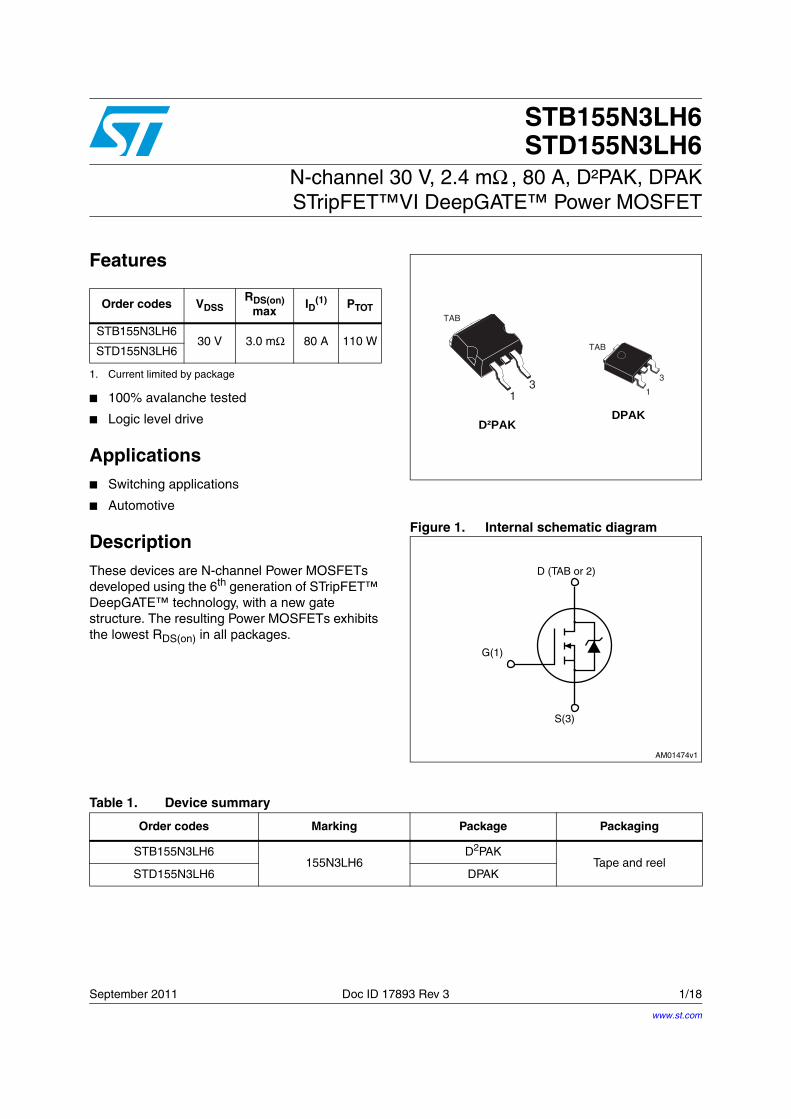
September 2011 Doc ID 17893 Rev 3 1/18 18 STB155N3LH6 STD155N3LH6 N-channel 30 V, 2.4 mΩ , 80 A, D²PAK, DPAK STripFET™VI DeepGATE™ Power MOSFET Features ■ 100% avalanche tested ■ Logic level drive Applications ■ Switching applications ■ Automotive Description These devices are N-channel Power MOSFETs developed using the 6 th generation of STripFET™ DeepGATE™ technology, with a new gate structure. The resulting Power MOSFETs exhibits the lowest R DS(on) in all packages. Figure 1. Internal schematic diagram Order codes V DSS R DS(on) max I D (1) 1. Current limited by package P TOT STB155N3LH6 30 V 3.0 mΩ 80 A 110 W STD155N3LH6 DPAK D²PAK 1 3 TAB TAB 3 1 Table 1. Device summary Order codes Marking Package Packaging STB155N3LH6 155N3LH6 D 2 PAK Tape and reel STD155N3LH6 DPAK www.st.com
Transcript of N-channel 30 V, 2.4 m , 80 A, D²PAK, DPAK STripFET VI ... · September 2011 Doc ID 17893 Rev 3...
September 2011 Doc ID 17893 Rev 3 1/18
18
STB155N3LH6STD155N3LH6
N-channel 30 V, 2.4 mΩ , 80 A, D²PAK, DPAKSTripFET™VI DeepGATE™ Power MOSFET
Features
100% avalanche tested
Logic level drive
Applications Switching applications
Automotive
DescriptionThese devices are N-channel Power MOSFETs developed using the 6th generation of STripFET™ DeepGATE™ technology, with a new gate structure. The resulting Power MOSFETs exhibits the lowest RDS(on) in all packages.
Figure 1. Internal schematic diagram
Order codes VDSSRDS(on)
maxID
(1)
1. Current limited by package
PTOT
STB155N3LH630 V 3.0 mΩ 80 A 110 W
STD155N3LH6
DPAKD²PAK
13
TAB
TAB
3
1
Table 1. Device summary
Order codes Marking Package Packaging
STB155N3LH6155N3LH6
D2PAKTape and reel
STD155N3LH6 DPAK
www.st.com

Contents STB155N3LH6, STD155N3LH6
2/18 Doc ID 17893 Rev 3
Contents
1 Electrical ratings . . . . . . . . . . . . . . . . . . . . . . . . . . . . . . . . . . . . . . . . . . . . 3
2 Electrical characteristics . . . . . . . . . . . . . . . . . . . . . . . . . . . . . . . . . . . . . 4
2.1 Electrical characteristics (curves) . . . . . . . . . . . . . . . . . . . . . . . . . . . . 6
3 Test circuits . . . . . . . . . . . . . . . . . . . . . . . . . . . . . . . . . . . . . . . . . . . . . . 8
4 Package mechanical data . . . . . . . . . . . . . . . . . . . . . . . . . . . . . . . . . . . . . 9
5 Packaging mechanical data . . . . . . . . . . . . . . . . . . . . . . . . . . . . . . . . . . 14
6 Revision history . . . . . . . . . . . . . . . . . . . . . . . . . . . . . . . . . . . . . . . . . . . 17

STB155N3LH6, STD155N3LH6 Electrical ratings
Doc ID 17893 Rev 3 3/18
1 Electrical ratings
Table 2. Absolute maximum ratings
Symbol Parameter Value Unit
VDS Drain-source voltage (VGS = 0) 30 V
VGS Gate-source voltage ± 20 V
ID (1)
1. Limited by wire bonding.
Drain current (continuous) at TC = 25 °C 80 A
ID Drain current (continuous) at TC = 100 °C 80 A
IDM (2)
2. Pulse width limited by safe operating area.
Drain current (pulsed) 320 A
PTOT Total dissipation at TC = 25 °C 110 W
Tstg Storage temperature-55 to 175
°C
Tj Operating junction temperature °C
Table 3. Thermal resistance
Symbol ParameterValue
UnitD2PAK DPAK
Rthj-case Thermal resistance junction-case max 1.36 °C/W
Rthj-pcb(1)
1. When mounted on 1 inch2 OZ Cu board.
Thermal resistance junction-pcb max 35 50 °C/W
Table 4. Thermal resistance
Symbol Parameter Value Unit
IAV Not-repetitive avalanche current 40 A
EAS (1)
1. Starting Tj = 25°C, ID = 40 A, VDD = 25 V
Single pulse avalanche energy 525 mJ
Electrical characteristics STB155N3LH6, STD155N3LH6
4/18 Doc ID 17893 Rev 3
2 Electrical characteristics
(TCASE = 25 °C unless otherwise specified).
Table 5. Static
Symbol Parameter Test conditions Min. Typ. Max. Unit
V(BR)DSSDrain-source breakdown voltage (VGS= 0)
ID = 250 µA 30 V
IDSSZero gate voltage drain current (VGS = 0)
VDS = 30 V
VDS = 30 V,Tc = 125 °C
1
10
µA
µA
IGSSGate body leakage current
(VDS = 0)VGS = ± 20 V ±100 nA
VGS(th) Gate threshold voltage VDS = VGS, ID = 250 µA 1 2.5 V
RDS(on)Static drain-source on resistance
VGS = 10 V, ID = 40 A 2.4 3.0 mΩ
VGS = 5 V, ID = 40 A 3.2 4.0 mΩ
Table 6. Dynamic
Symbol Parameter Test conditions Min Typ. Max. Unit
Ciss
Coss
Crss
Input capacitanceOutput capacitance
Reverse transfer capacitance
VDS = 25 V, f=1 MHz,
VGS = 0-
3800
725
420
-
pF
pF
pF
Qg
Qgs
Qgd
Total gate charge
Gate-source charge
Gate-drain charge
VDD = 15 V, ID = 80 A
VGS = 10 V
(see Figure 14)
-
80
15
15
-
nC
nC
nC
RG Gate input resistance
f = 1 MHz gate bias
Bias = 0 test signal
level = 20 mVopen drain
- 1.5 - Ω

STB155N3LH6, STD155N3LH6 Electrical characteristics
Doc ID 17893 Rev 3 5/18
Table 7. Switching on/off (inductive load)
Symbol Parameter Test conditions Min. Typ. Max. Unit
td(on)
tr
Turn-on delay time
Rise time
VDD = 15 V, ID = 40 A,
RG = 4.7 Ω, VGS = 10 V
(see Figure 15)
-15
85-
ns
ns
td(off)
tf
Turn-off delay timeFall time
VDD = 15 V, ID = 40 A,
RG = 4.7 Ω, VGS = 10 V
(see Figure 15)
-10040
-nsns
Table 8. Source drain diode
Symbol Parameter Test conditions Min. Typ. Max. Unit
ISD
ISDM(1)
1. Pulse width limited by safe operating area.
Source-drain currentSource-drain current (pulsed)
-80
320AA
VSD(2)
2. Pulsed: pulse duration = 300 µs, duty cycle 1.5%
Forward on voltage ISD = 40 A, VGS = 0 - 1.3 V
trrQrr
IRRM
Reverse recovery time
Reverse recovery chargeReverse recovery current
ISD = 80 A,
di/dt = 100 A/µs,
VDD = 24 V
(see Figure 17)
-
35
26.51.7
ns
nCA

Electrical characteristics STB155N3LH6, STD155N3LH6
6/18 Doc ID 17893 Rev 3
2.1 Electrical characteristics (curves) Figure 2. Safe operating area Figure 3. Thermal impedance
Figure 4. Output characteristics Figure 5. Transfer characteristics
Figure 6. Normalized BVDSS vs temperature Figure 7. Static drain-source on resistance
ID
100
10
10.1 1 VDS(V)10
(A)
Opera
tion
in th
is ar
ea is
Limite
d by
max
RDS(o
n)
100µs
1ms
10ms
Tj=175°CTc=25°CSingle pulse
AM09101v1
ID
150
100
50
00 1.0 VDS(V)
(A)
0.5 1.5
200
250
5V
4V
3V
VGS=10V300
AM09102v1ID
150
100
50
00 2 VGS(V)4
(A)
1 3
200
VDS=1V
AM09103v1
BVDSS
-75 TJ(°C)
(norm)
-25 7525 1250.80
0.85
0.90
0.95
1.00
1.05
ID=1mA1.10
AM09104v1RDS(on)
1.5
1.0
0.5
00 40 ID(A)
(mΩ)
20 60
2.0
2.5
3.0
3.5VGS=10V
80
AM09105v1
STB155N3LH6, STD155N3LH6 Electrical characteristics
Doc ID 17893 Rev 3 7/18
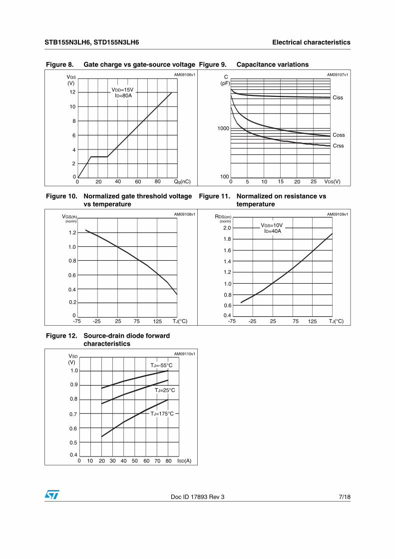
Figure 8. Gate charge vs gate-source voltage Figure 9. Capacitance variations
Figure 10. Normalized gate threshold voltage vs temperature
Figure 11. Normalized on resistance vs temperature
Figure 12. Source-drain diode forward characteristics
VGS
6
4
2
00 20 Qg(nC)
(V)
80
8
40 60
10
VDD=15VID=80A
12
AM09106v1 C
1000
1000 10 VDS(V)
(pF)
5 15
Ciss
Coss
Crss
20 25
AM09107v1
VGS(th)
0.6
0.4
0.2
0-75 TJ(°C)
(norm)
-25
0.8
7525 125
1.0
1.2
AM09108v1 RDS(on)
1.0
0.8
0.6
0.4-75 TJ(°C)
(norm)
-25 7525 125
1.6
1.4
1.2
2.0
1.8
VGS=10VID=40A
AM09109v1
VSD
0 20 ISD(A)
(V)
10 5030 400.4
0.5
0.6
0.7
0.8
0.9
1.0TJ=-55°C
TJ=175°C
TJ=25°C
8060 70
AM09110v1
Test circuits STB155N3LH6, STD155N3LH6
8/18 Doc ID 17893 Rev 3
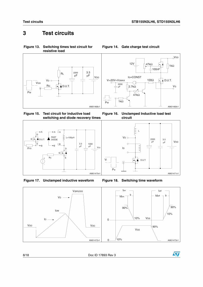
3 Test circuits
Figure 13. Switching times test circuit for resistive load
Figure 14. Gate charge test circuit
Figure 15. Test circuit for inductive load switching and diode recovery times
Figure 16. Unclamped Inductive load test circuit
Figure 17. Unclamped inductive waveform Figure 18. Switching time waveform
AM01468v1
VGS
PW
VD
RG
RL
D.U.T.
2200
µF3.3µF
VDD
AM01469v1
VDD
47kΩ 1kΩ
47kΩ
2.7kΩ
1kΩ
12V
Vi=20V=VGMAX
2200µF
PW
IG=CONST100Ω
100nF
D.U.T.
VG
AM01470v1
AD
D.U.T.
SB
G
25 Ω
A A
BB
RG
G
FASTDIODE
D
S
L=100µH
µF3.3 1000
µF VDD
AM01471v1
Vi
Pw
VD
ID
D.U.T.
L
2200µF
3.3µF VDD
AM01472v1
V(BR)DSS
VDDVDD
VD
IDM
ID
AM01473v1
VDS
ton
tdon tdoff
toff
tftr
90%
10%
10%
0
0
90%
90%
10%
VGS
STB155N3LH6, STD155N3LH6 Package mechanical data
Doc ID 17893 Rev 3 9/18
4 Package mechanical data
In order to meet environmental requirements, ST offers these devices in different grades of ECOPACK® packages, depending on their level of environmental compliance. ECOPACK® specifications, grade definitions and product status are available at: www.st.com. ECOPACK is an ST trademark.

Package mechanical data STB155N3LH6, STD155N3LH6
10/18 Doc ID 17893 Rev 3
Table 9. D²PAK (TO-263) mechanical data
Dim.mm
Min. Typ. Max.
A 4.40 4.60
A1 0.03 0.23
b 0.70 0.93
b2 1.14 1.70
c 0.45 0.60
c2 1.23 1.36
D 8.95 9.35
D1 7.50
E 10 10.40
E1 8.50
e 2.54
e1 4.88 5.28
H 15 15.85
J1 2.49 2.69
L 2.29 2.79
L1 1.27 1.40
L2 1.30 1.75
R 0.4
V2 0° 8°
STB155N3LH6, STD155N3LH6 Package mechanical data
Doc ID 17893 Rev 3 11/18
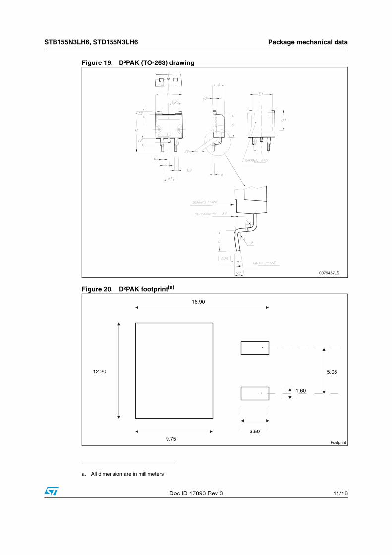
Figure 19. D²PAK (TO-263) drawing
Figure 20. D²PAK footprint(a)
a. All dimension are in millimeters
0079457_S
16.90
12.20
9.75
3.50
5.08
1.60
Footprint

Package mechanical data STB155N3LH6, STD155N3LH6
12/18 Doc ID 17893 Rev 3
Table 10. DPAK (TO-252) mechanical data
Dim.mm
Min. Typ. Max.
A 2.20 2.40
A1 0.90 1.10
A2 0.03 0.23
b 0.64 0.90
b4 5.20 5.40
c 0.45 0.60
c2 0.48 0.60
D 6.00 6.20
D1 5.10
E 6.40 6.60
E1 4.70
e 2.28
e1 4.40 4.60
H 9.35 10.10
L 1 1.50
L1 2.80
L2 0.80
L4 0.60 1
R 0.20
V2 0° 8°

STB155N3LH6, STD155N3LH6 Package mechanical data
Doc ID 17893 Rev 3 13/18
Figure 21. DPAK (TO-252) drawing
Figure 22. DPAK footprint(b)
b. All dimension are in millimeters
0068772_H
6.7
1.6
1.6
2.3
2.3
6.7 1.8 3
AM08850v1
Packaging mechanical data STB155N3LH6, STD155N3LH6
14/18 Doc ID 17893 Rev 3
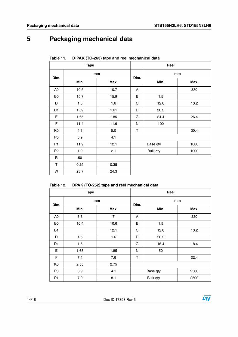
5 Packaging mechanical data
Table 11. D²PAK (TO-263) tape and reel mechanical data
Tape Reel
Dim.mm
Dim.mm
Min. Max. Min. Max.
A0 10.5 10.7 A 330
B0 15.7 15.9 B 1.5
D 1.5 1.6 C 12.8 13.2
D1 1.59 1.61 D 20.2
E 1.65 1.85 G 24.4 26.4
F 11.4 11.6 N 100
K0 4.8 5.0 T 30.4
P0 3.9 4.1
P1 11.9 12.1 Base qty 1000
P2 1.9 2.1 Bulk qty 1000
R 50
T 0.25 0.35
W 23.7 24.3
Table 12. DPAK (TO-252) tape and reel mechanical data
Tape Reel
Dim.mm
Dim.mm
Min. Max. Min. Max.
A0 6.8 7 A 330
B0 10.4 10.6 B 1.5
B1 12.1 C 12.8 13.2
D 1.5 1.6 D 20.2
D1 1.5 G 16.4 18.4
E 1.65 1.85 N 50
F 7.4 7.6 T 22.4
K0 2.55 2.75
P0 3.9 4.1 Base qty. 2500
P1 7.9 8.1 Bulk qty. 2500
STB155N3LH6, STD155N3LH6 Packaging mechanical data
Doc ID 17893 Rev 3 15/18
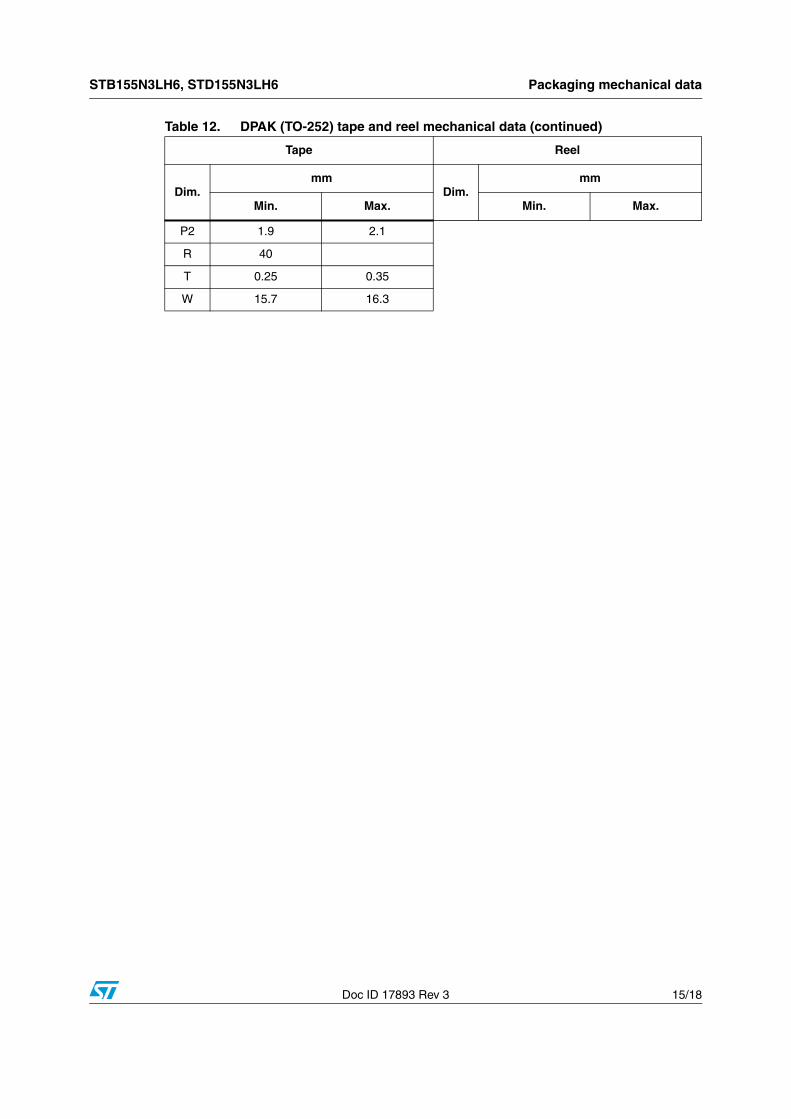
P2 1.9 2.1
R 40
T 0.25 0.35
W 15.7 16.3
Table 12. DPAK (TO-252) tape and reel mechanical data (continued)
Tape Reel
Dim.mm
Dim.mm
Min. Max. Min. Max.

Packaging mechanical data STB155N3LH6, STD155N3LH6
16/18 Doc ID 17893 Rev 3
Figure 23. Tape for D²PAK (TO-263) and DPAK (TO-252)
Figure 24. Reel for D²PAK (TO-263) and DPAK (TO-252)
P1A0 D1
P0
F
W
E
D
B0K0
T
User direction of feed
P2
10 pitches cumulativetolerance on tape +/- 0.2 mm
User direction of feed
R
Bending radius
Top covertape
AM08852v2
A
D
B
Full radius G measured at hub
C
N
REEL DIMENSIONS
40mm min.
Access hole
At sl ot location
T
Tape slot in core fortape start 25 mm min.width
AM08851v2
STB155N3LH6, STD155N3LH6 Revision history
Doc ID 17893 Rev 3 17/18
6 Revision history
Table 13. Document revision history
Date Revision Changes
02-Sep-2010 1 First release.
12-Apr-2011 2 Document status promoted from preliminary data to datasheet.
27-Sep-2011 3Updated Table 1: Device summary, Figure 2: Safe operating area and Section 4: Package mechanical data.
Minor text changes.
STB155N3LH6, STD155N3LH6
18/18 Doc ID 17893 Rev 3
Please Read Carefully:
Information in this document is provided solely in connection with ST products. STMicroelectronics NV and its subsidiaries (“ST”) reserve theright to make changes, corrections, modifications or improvements, to this document, and the products and services described herein at anytime, without notice.
All ST products are sold pursuant to ST’s terms and conditions of sale.
Purchasers are solely responsible for the choice, selection and use of the ST products and services described herein, and ST assumes noliability whatsoever relating to the choice, selection or use of the ST products and services described herein.
No license, express or implied, by estoppel or otherwise, to any intellectual property rights is granted under this document. If any part of thisdocument refers to any third party products or services it shall not be deemed a license grant by ST for the use of such third party productsor services, or any intellectual property contained therein or considered as a warranty covering the use in any manner whatsoever of suchthird party products or services or any intellectual property contained therein.
UNLESS OTHERWISE SET FORTH IN ST’S TERMS AND CONDITIONS OF SALE ST DISCLAIMS ANY EXPRESS OR IMPLIEDWARRANTY WITH RESPECT TO THE USE AND/OR SALE OF ST PRODUCTS INCLUDING WITHOUT LIMITATION IMPLIEDWARRANTIES OF MERCHANTABILITY, FITNESS FOR A PARTICULAR PURPOSE (AND THEIR EQUIVALENTS UNDER THE LAWSOF ANY JURISDICTION), OR INFRINGEMENT OF ANY PATENT, COPYRIGHT OR OTHER INTELLECTUAL PROPERTY RIGHT.
UNLESS EXPRESSLY APPROVED IN WRITING BY TWO AUTHORIZED ST REPRESENTATIVES, ST PRODUCTS ARE NOTRECOMMENDED, AUTHORIZED OR WARRANTED FOR USE IN MILITARY, AIR CRAFT, SPACE, LIFE SAVING, OR LIFE SUSTAININGAPPLICATIONS, NOR IN PRODUCTS OR SYSTEMS WHERE FAILURE OR MALFUNCTION MAY RESULT IN PERSONAL INJURY,DEATH, OR SEVERE PROPERTY OR ENVIRONMENTAL DAMAGE. ST PRODUCTS WHICH ARE NOT SPECIFIED AS "AUTOMOTIVEGRADE" MAY ONLY BE USED IN AUTOMOTIVE APPLICATIONS AT USER’S OWN RISK.
Resale of ST products with provisions different from the statements and/or technical features set forth in this document shall immediately voidany warranty granted by ST for the ST product or service described herein and shall not create or extend in any manner whatsoever, anyliability of ST.
ST and the ST logo are trademarks or registered trademarks of ST in various countries.
Information in this document supersedes and replaces all information previously supplied.
The ST logo is a registered trademark of STMicroelectronics. All other names are the property of their respective owners.
© 2011 STMicroelectronics - All rights reserved
STMicroelectronics group of companies
Australia - Belgium - Brazil - Canada - China - Czech Republic - Finland - France - Germany - Hong Kong - India - Israel - Italy - Japan - Malaysia - Malta - Morocco - Philippines - Singapore - Spain - Sweden - Switzerland - United Kingdom - United States of America
www.st.com