MUZAFFARPUR INSTITUTE OF TECHNOLOGY, Muzaffarpur › wp-content › uploads › ... · MUZAFFARPUR...
26
1 | Page MUZAFFARPUR INSTITUTE OF TECHNOLOGY, Muzaffarpur COURSE FILE OF SOLID STATE PHYSICS AND DEVICES (041308) Faculty Name: Mr. RAVI KUMAR ASSISTANT PROFESSOR,
Transcript of MUZAFFARPUR INSTITUTE OF TECHNOLOGY, Muzaffarpur › wp-content › uploads › ... · MUZAFFARPUR...

1 | P a g e
MUZAFFARPUR INSTITUTE OF TECHNOLOGY,
Muzaffarpur
COURSE FILE
OF
SOLID STATE PHYSICS AND DEVICES
(041308)
Faculty Name:
Mr. RAVI KUMAR
ASSISTANT PROFESSOR,

2 | P a g e
DEPARTMENT OF ELECTRONICS AND COMMUNICATION
ENGINEERING
Content
S.No. Topic Page No.
1 Vision of department 3
2 Mission of department 4
3 PEO’s 5
4 PO’s 6
5 Course objectives and course outcomes(CO) 8
6 Mapping of CO’s with PO’s 9
7 Course syllabus and GATE syllabus 10
8 Time table
12
9 Student list
14
10 Textbook / Reference Books 18
11 Course plan 19
12 Assignments
21
13 Question Bank
27
14 List of Experiments 42

3 | P a g e
VISION OF DEPARTMENT
The department is committed for high quality teaching and pursuit of excellence in research.
We pledge to serve the nation and society by providing skilled and well developed human
resource through brilliance in technical education and research.
4 | P a g e
MISSION OF DEPARTMENT
• To encourage innovation and research through projects and developmental activities
with industries, institutions and government.
• To inculcate moral and ethical values with a sense of competitiveness, self-confidence
and sincerity among the students to make them a good human and a good citizen.
• To produce excellent engineers, innovators, entrepreneurs and academicians for the
growth of the society.

5 | P a g e
PROGRAMME EDUCATIONAL OBJECTIVES (PEOs):
After successful completion of program, graduates will be able to
PEO1: Work in the infrastructure development projects.
PEO2: Pursue higher studies.
PEO3: Contribute in teaching, research and other developmental activities of
electronics & communication engineering and its allied fields.
PEO4: Work in the multicultural and multidisciplinary groups for the sustainable
development and growth of electronics and communication engineering projects and
profession.

6 | P a g e
PROGRAMME OUTCOMES (PO)
PO1
Engineering knowledge: Apply the knowledge of mathematics, science, engineering
fundamentals, and an engineering specialization to the solution of complex engineering
problems.
PO2 Problem analysis: Identify, formulate, review research literature, and analyze complex
engineering problems reaching substantiated conclusions using first principles of
mathematics, natural sciences, and engineering sciences.
PO3 Design/development of solutions: Design solutions for complex engineering problems
and design system components or processes that meet the specified needs with
appropriate consideration for the public health and safety, and the cultural, societal, and
environmental considerations.
PO4 Conduct investigations of complex problems: Use research-based knowledge and
research methods including design of experiments, analysis and interpretation of
data, and synthesis of the information to provide valid conclusions.
PO5 Modern tool usage: Create, select, and apply appropriate techniques, resources, and
modern engineering and IT tools including prediction and modeling to complex
engineering activities with an understanding of the limitations.
PO6 The engineer and society: Apply reasoning informed by the contextual knowledge to
assess societal, health, safety, legal and cultural issues and the consequent
responsibilities relevant to the professional engineering practice.
PO7 Environment and sustainability: Understand the impact of the professional
engineering solutions in societal and environmental contexts, and demonstrate the
knowledge of and need for sustainable development.
PO8 Ethics: Apply ethical principles and commit to professional ethics and responsibilities

7 | P a g e
and norms of the engineering practice.
PO9 Individual and teamwork: Function effectively as an individual, and as a member or
leader in diverse teams, and in multidisciplinary settings.
PO10 Communication: Communicate effectively on complex engineering activities with the
engineering community and with society at large, such as, being able to comprehend and
write effective reports and design documentation, make effective presentations, and give
and receive clear instructions.
PO11 Project management and finance: Demonstrate knowledge and understanding of the
engineering and management principles and apply these to one's own work, as
a member and leader in a team, to manage projects and in multidisciplinary
environments.
PO12 Life-long learning: Recognize the need for, and have the preparation and ability to
engage in independent and life-long learning in the broadest context of technological
change.
8 | P a g e
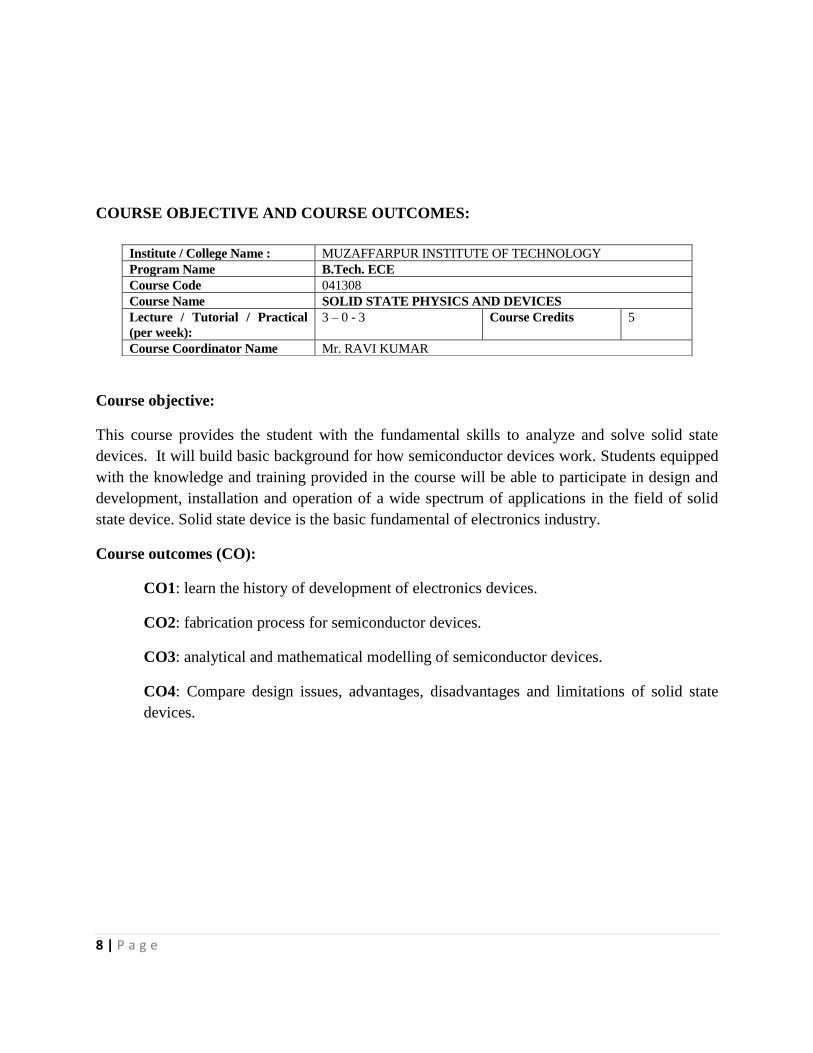
COURSE OBJECTIVE AND COURSE OUTCOMES:
Course objective:
This course provides the student with the fundamental skills to analyze and solve solid state
devices. It will build basic background for how semiconductor devices work. Students equipped
with the knowledge and training provided in the course will be able to participate in design and
development, installation and operation of a wide spectrum of applications in the field of solid
state device. Solid state device is the basic fundamental of electronics industry.
Course outcomes (CO):
CO1: learn the history of development of electronics devices.
CO2: fabrication process for semiconductor devices.
CO3: analytical and mathematical modelling of semiconductor devices.
CO4: Compare design issues, advantages, disadvantages and limitations of solid state
devices.
Institute / College Name : MUZAFFARPUR INSTITUTE OF TECHNOLOGY
Program Name B.Tech. ECE
Course Code 041308
Course Name SOLID STATE PHYSICS AND DEVICES
Lecture / Tutorial / Practical
(per week):
3 – 0 - 3 Course Credits 5
Course Coordinator Name Mr. RAVI KUMAR
9 | P a g e
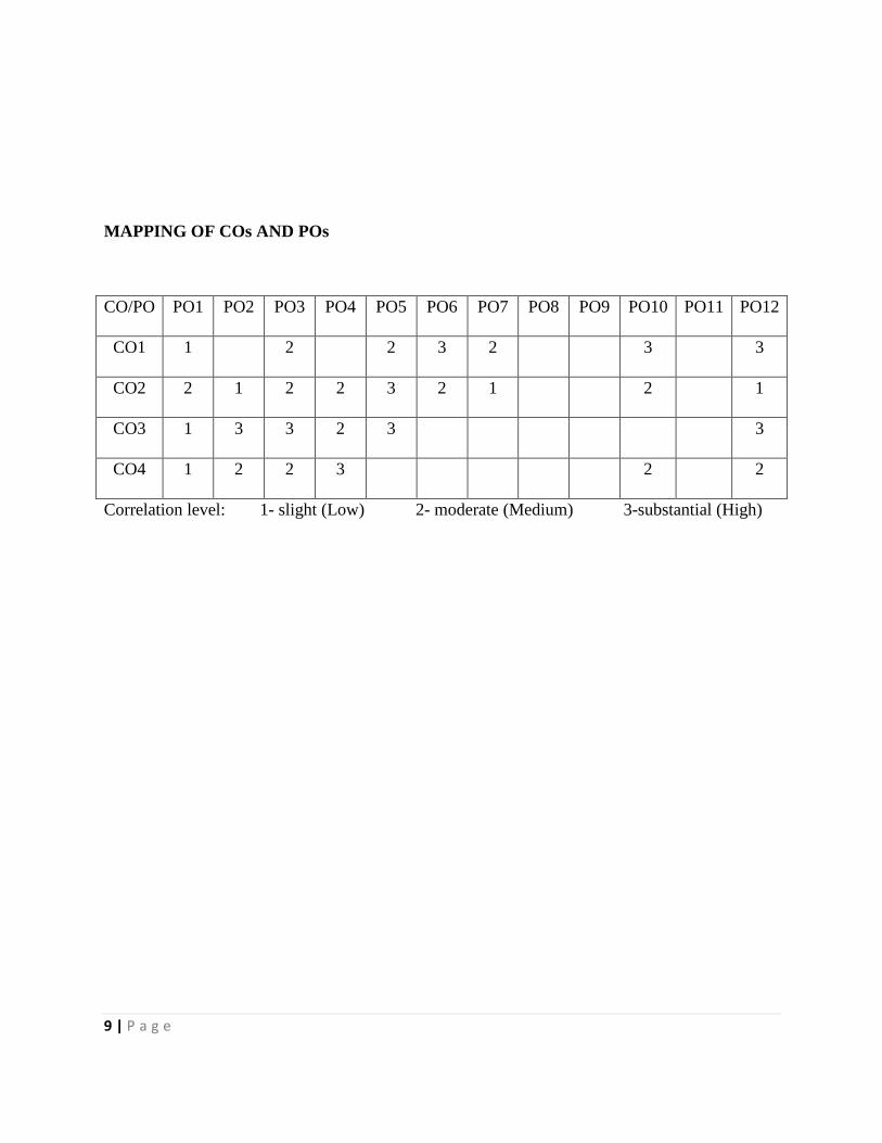
MAPPING OF COs AND POs
CO/PO PO1 PO2 PO3 PO4 PO5 PO6 PO7 PO8 PO9 PO10 PO11 PO12
CO1 1 2 2 3 2 3 3
CO2 2 1 2 2 3 2 1 2 1
CO3 1 3 3 2 3 3
CO4 1 2 2 3 2 2
Correlation level: 1- slight (Low) 2- moderate (Medium) 3-substantial (High)
10 | P a g e
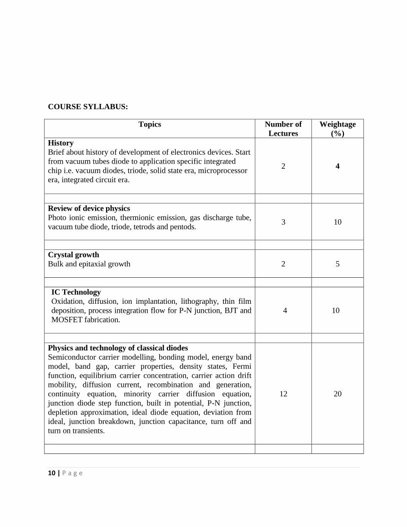
COURSE SYLLABUS:
Topics Number of
Lectures
Weightage
(%)
History
Brief about history of development of electronics devices. Start
from vacuum tubes diode to application specific integrated
chip i.e. vacuum diodes, triode, solid state era, microprocessor
era, integrated circuit era.
2 4
Review of device physics
Photo ionic emission, thermionic emission, gas discharge tube,
vacuum tube diode, triode, tetrods and pentods. 3 10
Crystal growth
Bulk and epitaxial growth
2 5
1. IC Technology
2. Oxidation, diffusion, ion implantation, lithography, thin film
deposition, process integration flow for P-N junction, BJT and
MOSFET fabrication.
3.
4 10
Physics and technology of classical diodes
Semiconductor carrier modelling, bonding model, energy band
model, band gap, carrier properties, density states, Fermi
function, equilibrium carrier concentration, carrier action drift
mobility, diffusion current, recombination and generation,
continuity equation, minority carrier diffusion equation,
junction diode step function, built in potential, P-N junction,
depletion approximation, ideal diode equation, deviation from
ideal, junction breakdown, junction capacitance, turn off and
turn on transients.
12 20

11 | P a g e
Physics and technology of BJT
Operation consideration, modes and configuration, base
transport factor, performance parameters, common base current
gain, small scale modelling, common emitter gain, base width
modulation, qualitative approach to understand switch response.
7 20
Physics and technology of FET
Junction FET theory of application, I-V characteristics, mos
capacitor, MOSFET theory of operation, non ideal MOSFET.
5 15
Properties and technology of UJT and SCR
Silicon controlled rectifier, uni junction transistor (theory of
operation)
2 6
Photonics
Photo diode, solar cell, solid state LASER diodes
3 6
CCD and CCD camera 2 4
12 | P a g e
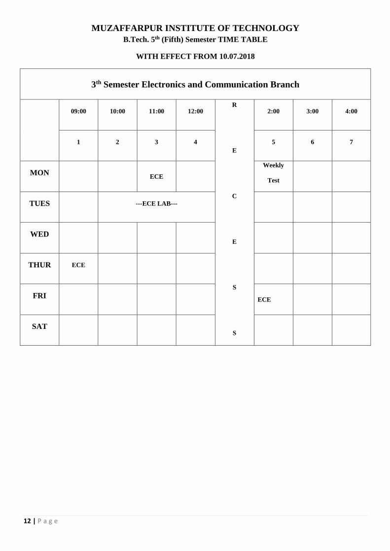
MUZAFFARPUR INSTITUTE OF TECHNOLOGY
B.Tech. 5th (Fifth) Semester TIME TABLE
WITH EFFECT FROM 10.07.2018
3th Semester Electronics and Communication Branch
09:00 10:00 11:00 12:00 R
E
C
E
S
S
2:00 3:00 4:00
1 2 3 4 5 6 7
MON ECE
Weekly
Test
TUES ---ECE LAB---
WED
THUR ECE
FRI ECE
SAT
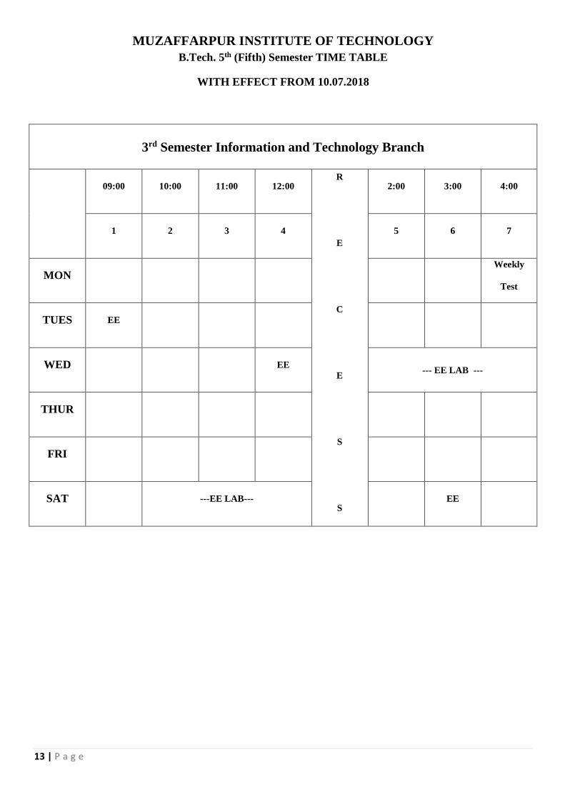
13 | P a g e
MUZAFFARPUR INSTITUTE OF TECHNOLOGY
B.Tech. 5th (Fifth) Semester TIME TABLE
WITH EFFECT FROM 10.07.2018
3rd Semester Information and Technology Branch
09:00 10:00 11:00 12:00 R
E
C
E
S
S
2:00 3:00 4:00
1 2 3 4 5 6 7
MON
Weekly
Test
TUES EE
WED EE --- EE LAB ---
THUR
FRI
SAT ---EE LAB--- EE
14 | P a g e
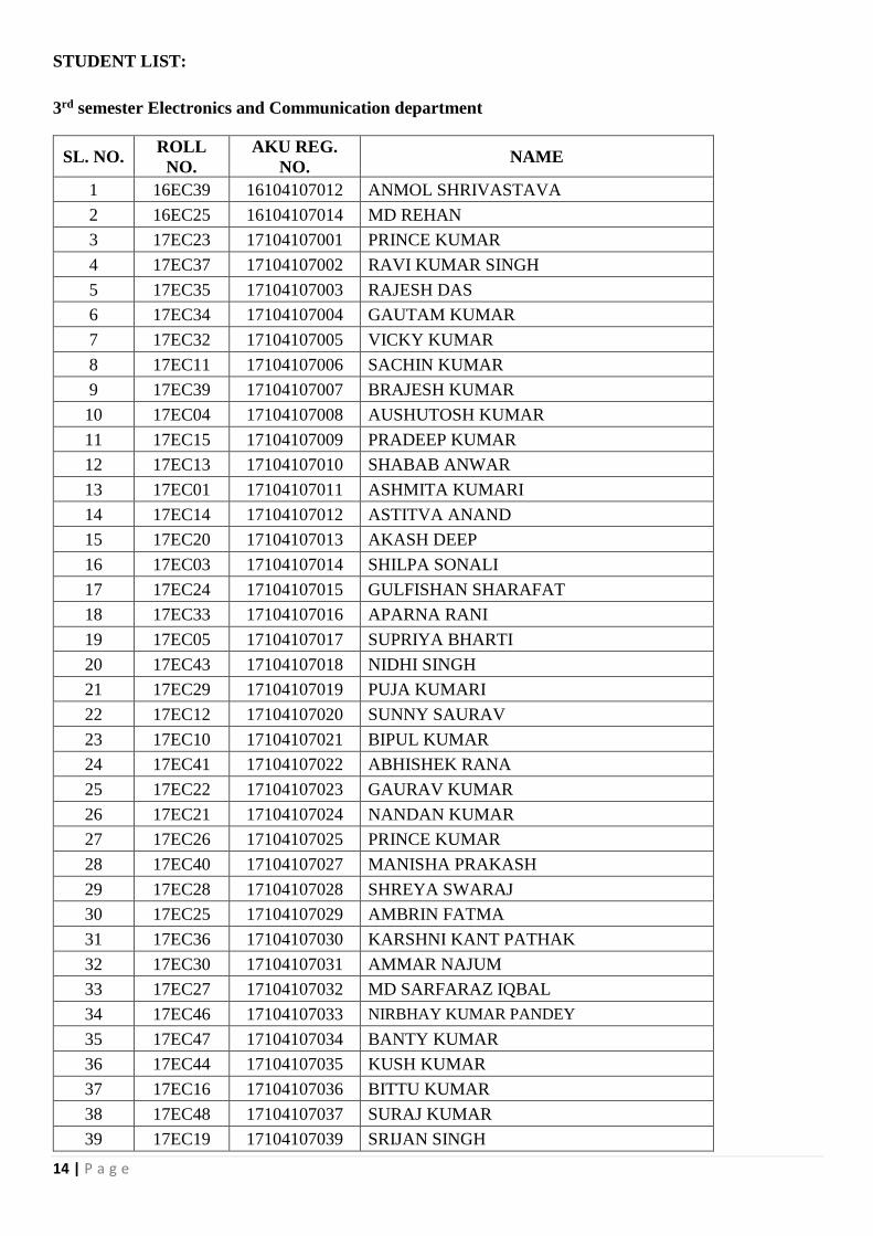
STUDENT LIST:
3rd semester Electronics and Communication department
SL. NO. ROLL
NO.
AKU REG.
NO. NAME
1 16EC39 16104107012 ANMOL SHRIVASTAVA
2 16EC25 16104107014 MD REHAN
3 17EC23 17104107001 PRINCE KUMAR
4 17EC37 17104107002 RAVI KUMAR SINGH
5 17EC35 17104107003 RAJESH DAS
6 17EC34 17104107004 GAUTAM KUMAR
7 17EC32 17104107005 VICKY KUMAR
8 17EC11 17104107006 SACHIN KUMAR
9 17EC39 17104107007 BRAJESH KUMAR
10 17EC04 17104107008 AUSHUTOSH KUMAR
11 17EC15 17104107009 PRADEEP KUMAR
12 17EC13 17104107010 SHABAB ANWAR
13 17EC01 17104107011 ASHMITA KUMARI
14 17EC14 17104107012 ASTITVA ANAND
15 17EC20 17104107013 AKASH DEEP
16 17EC03 17104107014 SHILPA SONALI
17 17EC24 17104107015 GULFISHAN SHARAFAT
18 17EC33 17104107016 APARNA RANI
19 17EC05 17104107017 SUPRIYA BHARTI
20 17EC43 17104107018 NIDHI SINGH
21 17EC29 17104107019 PUJA KUMARI
22 17EC12 17104107020 SUNNY SAURAV
23 17EC10 17104107021 BIPUL KUMAR
24 17EC41 17104107022 ABHISHEK RANA
25 17EC22 17104107023 GAURAV KUMAR
26 17EC21 17104107024 NANDAN KUMAR
27 17EC26 17104107025 PRINCE KUMAR
28 17EC40 17104107027 MANISHA PRAKASH
29 17EC28 17104107028 SHREYA SWARAJ
30 17EC25 17104107029 AMBRIN FATMA
31 17EC36 17104107030 KARSHNI KANT PATHAK
32 17EC30 17104107031 AMMAR NAJUM
33 17EC27 17104107032 MD SARFARAZ IQBAL
34 17EC46 17104107033 NIRBHAY KUMAR PANDEY
35 17EC47 17104107034 BANTY KUMAR
36 17EC44 17104107035 KUSH KUMAR
37 17EC16 17104107036 BITTU KUMAR
38 17EC48 17104107037 SURAJ KUMAR
39 17EC19 17104107039 SRIJAN SINGH

15 | P a g e
40 17EC45 17104107040 MD SHERIQUE ANWAR
41 17EC42 17104107041 ROHIT KUMAR
42 17EC38 17104107042 AADIL RAZA
43 17EC06 17104107043 SUPRIYA KUMARI
3rd semester Electrical Engineering department
SL.
NO.
ROLL
NO. AKU REG. NO. NAME
1 16E47 16103107020 SHUBHAM KUMAR
2 17E01 17103107001 SHIVANGI
3 17E24 17103107002 PRAGYA KUMARI
4 17E04 17103107003 KANNU PRIYA
5 17E08 17103107004 VIDYA KUMARI
6 17E07 17103107005 APARNA SINGH
7 17E13 17103107006 KHUSHBOO ANAND
8 17E09 17103107007 VIVEK KUMAR
9 17E03 17103107008 SHIVAM DUBEY
10 17E17 17103107009 VANDANA BHARTI
11 17E16 17103107010 SANDHYA KUMARI
12 17E19 17103107011 NEHA SINGH
13 17E10 17103107013 ABHIJEET KUMAR
14 17E12 17103107014 NIRAJ KUMAR
15 17E02 17103107015 SAURAV SINHA
16 17E22 17103107016 ABHINAV KISHORE
17 17E25 17103107017 GAUTAM KUMAR
18 17E11 17103107018 UTPAL KANT
19 17E26 17103107019 ASHUTOSH KUMAR
20 17E21 17103107020 DEPAK KUMAR
21 17E42 17103107021 RAVI PRAKASH CHOUDHARY
22 17E06 17103107022 SAURAV KUMAR
23 17E34 17103107023 PAVAN KUMAR
24 17E23 17103107024 SINTU KUMAR
25 17E55 17103107025 GHANSHYAM KUMAR
26 17E18 17103107026 SATYA PRAKASH
27 17E48 17103107027 ASHISH KUMAR
28 17E20 17103107028 MOHAMMAD EHSHANULLAH
16 | P a g e
29 17E30 17103107029 MASYOOD AHMAD
30 17E60 17103107030 ABHIMANYU KUMAR SINGH
31 17E29 17103107031 SUMIT KUMAR
32 17E44 17103107032 PRIYA KUMARI
33 17E32 17103107033 NELSHAN RANI
34 17E47 17103107034 VIKASH KUMAR
35 17E51 17103107035 ROHIT KUMAR
36 17E31 17103107036 VANISHA SHARMA
37 17E58 17103107037 MANISH KUMAR
38 17E61 17103107038 SWETA KUMARI
39 17E38 17103107039 ABHISHEK RAJ
40 17E33 17103107040 SANDEEP KUMAR SINHA
41 17E36 17103107041 ANAMIKA BHARTI
42 17E41 17103107042 RAVISHANKAR KUMAR
43 17E53 17103107043 MITHUN KUMAR
44 17E63 17103107044 NAVNEET NAYAN
45 17E28 17103107045 KUMAR ARYAN
46 17E64 17103107046 AMIT KUMAR
47 17E37 17103107047 TAMANNA CHOUDHARY
48 17E56 17103107048 ASHWINI KUMAR
49 17E39 17103107049 PRAVEEN KUMAR SAFI
50 17E35 17103107050 NAVIN PUSHKAR
51 17E52 17103107051 PREM BHARTI
52 17E59 17103107052 SANTOSH KUMAR RAM
53 17E40 17103107053 ANAMIKA KAUSHIK
54 17E43 17103107054 BUNTY KUMAR PASWAN
55 17E50 17103107055 AMAN RAJ
56 17E15 17103107056 RAJ KAMAL
57 17E45 17103107057 RAMBABU BAITHA
58 17E62 17103107058 RAJSHEKHAR KUMAR GOKUL
59 17E57 17103107059 RAHAT ARAFAT
60 17E54 17103107060 SUSHIL KUMAR
17 | P a g e
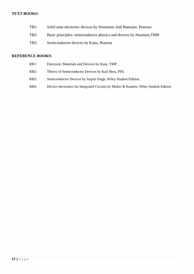
TEXT BOOKS:
TB1: Solid state electronic devices by Streetmen And Banerjee, Pearson:
TB2: Basic principles- semiconductor physics and devices by Nearmen,TMH
TB3: Semiconductor devices by Kano, Pearson
REFERENCE BOOKS:
RB1: Electronic Materials and Devices by Kasp. TMP.
RB2: Theory of Semiconductor Devices by Karl Hess, PHI.
RB3: Semiconductor Devices by Jasprit Singh, Wiley Student Edition.
RB4: Device electronics for Integrated Circuits by Muller & Kamins, Wiley Student Edition

18 | P a g e
COURSE PLAN
Lecture
Number
Topics Web Links for video
lectures
Text Book /
Reference
Book
Page
numbers of
Book
1-2 HISTORY
Brief about history of development of
electronics devices. Start from
vacuum tubes diode to application
specific integrated chip i.e. vacuum
diodes, triode, solid state era,
microprocessor era, integrated circuit
era.
3-5 REVIEW OF DEVICE PHYSICS
Photo ionic emission, thermionic
emission, gas discharge tube, vacuum
tube diode, triode, tetrods and pentods.
6-7 Crystal growth
Bulk and epitaxial growth
8-11 IC Technology
Oxidation, diffusion, ion implantation,
lithography, thin film deposition,
process integration flow for P-N
junction, BJT and MOSFET
fabrication
12-23 Physics and technology of classical
diodes
Semiconductor carrier modelling,
bonding model, energy band model,
band gap, carrier properties, density
states, Fermi function, equilibrium
carrier concentration, carrier action
drift mobility, diffusion current,
recombination and generation,
continuity equation, minority carrier

19 | P a g e
diffusion equation, junction diode
step function, built in potential, P-N
junction, depletion approximation,
ideal diode equation, deviation from
ideal, junction breakdown, junction
capacitance, turn off and turn on
transients.
24-30 Physics and technology of BJT
Operation consideration, modes and
configuration, base transport factor,
performance parameters, common
base current gain, small scale
modelling, common emitter gain, base
width modulation, qualitative
approach to understand switch
response.
31-36 Physics and technology of FET
Junction FET theory of application, I-
V characteristics, MOS capacitor,
MOSFET theory of operation, non-
ideal MOSFET.
36-38 Properties and technology of UJT
and SC
Silicon controlled rectifier, uni
junction transistor (theory of
operation)
38-41 Photonics
Photo diode, solar cell, laser diode
41-43 CCD and CCD camera
Charge couple device theroy

20 | P a g e
DETAILS OF ASSIGNMENTS:
S.No. Assignment Unit wise
1 Assignment 1 Unit 1 and unit 2
2 Assignment 2 Unit 3 and unit 4
3 Assignment 3 Unit 5 and unit 6
4 Assignment 4 Unit 7 unit 8 and unit 9

21 | P a g e
ASSIGNMENT 1
ASSIGNMENT 2
ASSIGNMENT 3
ASSIGNMENT 4

22 | P a g e
QUESTION BANK:

23 | P a g e

24 | P a g e

25 | P a g e

26 | P a g e
LIST OF THE EXPERIMENT
1. To determine the energy gap of PN junction.
2. To study of I-V characteristic of SCR.
3. To study of I-V characteristic of UJT.
4. To study of I-V characteristic of triac.
5. To study of I-V characteristic of photodiode.
6. To study of I-V characteristic of LED.
7. To study of I-V characteristic of tunnel diode.
8. To study of I-V characteristic of varactor diode.
9. To study of I-V characteristic of zener diode.
10. To study of transfer function and output characteristic of MOSFET.