Multiple soft fault diagnosis of DC analog CMOS circuits ... · Multiple soft fault diagnosis of DC...
13
Multiple soft fault diagnosis of DC analog CMOS circuits designed in nanometer technology Michal Tadeusiewicz 1 • Stanislaw Halgas 1 Received: 3 November 2015 / Revised: 11 February 2016 / Accepted: 21 April 2016 / Published online: 6 May 2016 Ó The Author(s) 2016. This article is published with open access at Springerlink.com Abstract This paper is devoted to local multiple soft fault diagnosis of nonlinear DC analog CMOS circuits designed in nanometer technology. An algorithm is developed that allows estimating the values of a set of potentially faulty process parameters. It exploits two tests with the input nodes accessible for excitation and the output node accessible for measurement. One of the tests is used to find the parameter values. It leads to a system of nonlinear algebraic type equations that are not given in explicit analytical form and may be satisfied by several sets of the parameter values. To solve the system of the equations the Nelder–Mead optimization method is applied with the objective function properly modified during the computa- tion process. Next the obtained solution, being a set of the parameter values, is validated using the other test. If the solution passes this test it is considered as the actual one. Otherwise, another solution is calculated and verified using the same approach. The developed diagnostic procedure has been implemented in DELPHI, whereas the required by the algorithm circuit analyses are performed using IsSPICE 4 and both environments have been joined together. For illustration three numerical examples are given. Keywords Analog nonlinear circuits Fault diagnosis Multiple soft faults Nanometer technology Nelder–Mead method 1 Introduction Fault diagnosis of analog circuits is an important problem in the design and testing of electronic devices [1–22]. Generally, fault diagnosis includes detecting faulty circuits, locating faulty parameters and evaluating their values. If a faulty parameter is drifted from its tolerance range but does not lead to some topological changes, the fault is said to be soft or parametric. If a fault is open circuit or short circuit, it is called hard or catastrophic. In integrated circuits physical imperfections, such as near–opens or near–shorts may occur as spot defects [7, 10, 21, 22]. The methods dedicated to soft fault diagnosis usually exploit the simu- lation after test approach, where circuit simulations take place after any testing. They are based on measurements of the voltages at accessible points of the circuit, leading to equations with the tested parameters as unknown variables. In current CMOS technology the global variations of parameters are measured by dedicated test structures included in the wafer. However, the problem is how to identify the random local variations of the process parameters. The local variations are due to fabrication or due to aging phenomenon. They affect the components across the die independently. Examples of local variations in ICs include local geometrical deformations, such as variations in the channel length and width, the oxide thickness, etc. Many concepts and methods focused on parametric fault diagnosis are presented in references [1–3, 5, 9, 11, 13, 16– 20]. Most of the works, dealing with soft fault diagnosis of analog circuits, address only the case when just one parameter is faulty. Fewer papers are devoted to the mul- tiple fault diagnosis, where several parameters can be faulty. In real circuits the test equations, that express the measured voltages in terms of the parameters are nonlinear & Michal Tadeusiewicz [email protected] 1 Department of Electrical, Electronic, Computer and Control Engineering, Lo ´dz ´ University of Technology, ul. Stefanowskiego 18/22, 90-924 Lo ´dz ´, Poland 123 Analog Integr Circ Sig Process (2016) 88:65–77 DOI 10.1007/s10470-016-0752-y
Transcript of Multiple soft fault diagnosis of DC analog CMOS circuits ... · Multiple soft fault diagnosis of DC...

Multiple soft fault diagnosis of DC analog CMOS circuits designedin nanometer technology
Michał Tadeusiewicz1• Stanisław Hałgas1
Received: 3 November 2015 / Revised: 11 February 2016 / Accepted: 21 April 2016 / Published online: 6 May 2016
� The Author(s) 2016. This article is published with open access at Springerlink.com
Abstract This paper is devoted to local multiple soft fault
diagnosis of nonlinear DC analog CMOS circuits designed
in nanometer technology. An algorithm is developed that
allows estimating the values of a set of potentially faulty
process parameters. It exploits two tests with the input
nodes accessible for excitation and the output node
accessible for measurement. One of the tests is used to find
the parameter values. It leads to a system of nonlinear
algebraic type equations that are not given in explicit
analytical form and may be satisfied by several sets of the
parameter values. To solve the system of the equations the
Nelder–Mead optimization method is applied with the
objective function properly modified during the computa-
tion process. Next the obtained solution, being a set of the
parameter values, is validated using the other test. If the
solution passes this test it is considered as the actual one.
Otherwise, another solution is calculated and verified using
the same approach. The developed diagnostic procedure
has been implemented in DELPHI, whereas the required by
the algorithm circuit analyses are performed using IsSPICE
4 and both environments have been joined together. For
illustration three numerical examples are given.
Keywords Analog nonlinear circuits � Fault diagnosis �Multiple soft faults � Nanometer technology � Nelder–Mead
method
1 Introduction
Fault diagnosis of analog circuits is an important problem
in the design and testing of electronic devices [1–22].
Generally, fault diagnosis includes detecting faulty circuits,
locating faulty parameters and evaluating their values. If a
faulty parameter is drifted from its tolerance range but does
not lead to some topological changes, the fault is said to be
soft or parametric. If a fault is open circuit or short circuit,
it is called hard or catastrophic. In integrated circuits
physical imperfections, such as near–opens or near–shorts
may occur as spot defects [7, 10, 21, 22]. The methods
dedicated to soft fault diagnosis usually exploit the simu-
lation after test approach, where circuit simulations take
place after any testing. They are based on measurements of
the voltages at accessible points of the circuit, leading to
equations with the tested parameters as unknown variables.
In current CMOS technology the global variations of
parameters are measured by dedicated test structures
included in the wafer. However, the problem is how to
identify the random local variations of the process
parameters. The local variations are due to fabrication or
due to aging phenomenon. They affect the components
across the die independently. Examples of local variations
in ICs include local geometrical deformations, such as
variations in the channel length and width, the oxide
thickness, etc.
Many concepts and methods focused on parametric fault
diagnosis are presented in references [1–3, 5, 9, 11, 13, 16–
20]. Most of the works, dealing with soft fault diagnosis of
analog circuits, address only the case when just one
parameter is faulty. Fewer papers are devoted to the mul-
tiple fault diagnosis, where several parameters can be
faulty. In real circuits the test equations, that express the
measured voltages in terms of the parameters are nonlinear
& Michał Tadeusiewicz
1 Department of Electrical, Electronic, Computer and Control
Engineering, Łodz University of Technology, ul.
Stefanowskiego 18/22, 90-924 Łodz, Poland
123
Analog Integr Circ Sig Process (2016) 88:65–77
DOI 10.1007/s10470-016-0752-y

and cannot be presented in explicit analytical form. These
equations may actually have multiple solutions, which
means that several sets of the parameter values meet the
test. To find the multiple solutions the parametric homo-
topy [17], the simplicial homotopy [18], or the block
relaxation method [19] were proposed. To determine the
actual solution a new efficient approach was proposed in
Ref. [20] as follows. Two tests of the circuit are arranged,
one used to find the solutions and the other to check if the
obtained solution is the actual one. To compute the solution
the extended systematic search method was developed
[20]. In this paper the Nelder–Mead optimization method is
applied with the objective function properly modified
during the computation process and similarly as in [20] the
obtained result is checked using the validation test. If the
obtained solution passes this test the algorithm terminates,
otherwise another solution is calculated and verified. The
procedure is carried out as long as the solution which meets
the validation test is obtained.
2 Diagnostic tests
Let us consider a nonlinear DC circuit, with n parameters
x1; . . .; xn considered as potentially faulty, having one or
more input nodes accessible for excitation and one output
node accessible for measurement. We connect to the output
node a resistor Ro and apply DC voltage sources to the
input nodes (see Fig. 1). We choose n sets of the input
voltage values and read the corresponding values of the
output voltage. They are labelled v1ð Þ
o ; . . .; vnð Þ
o and used to
form vector v oð Þ ¼ v1ð Þ
o � � � v nð Þo
h i T
, where T means trans-
position. Each of the voltages is a function of the circuit
parameters x1; . . .; xn, vjð Þ
o ¼ ~gj xð Þ, where x ¼ x1 � � � xn½ �T
is the vector consisting of the parameters considered as
potentially faulty. Thus, it holds
v oð Þ ¼ ~g xð Þ; ð1Þ
where ~g xð Þ ¼ ~g1 xð Þ � � � ~gn xð Þ½ �T. Equation (1) can be
rewritten in the compact form
g xð Þ ¼ 0; ð2Þ
where g xð Þ ¼ g1 xð Þ � � � gn xð Þ½ �T¼ ~g xð Þ � v oð Þ, and named
a test equation.
The diagnostic method developed in Sect. 3 requires
two tests arranged using the above–described approach. As
a result the voltages v1ð Þ
o ; . . .; vnð Þ
o are measured in the
circuit as depicted in Fig. 1, but driven by different sets of
the input voltage sources, forming vector v oð Þ ¼
v1ð Þ
o � � � v nð Þo
h i T
. The first test leading to Eq. (2) will be
named a principal test (PT), whereas the second one will be
named a validation test (VT).
Unfortunately, in real electronic circuits the function
g xð Þ cannot be presented in explicit analytical form.
However, the values of ~gi xð Þ i ¼ 1; . . .; n, for given x, can
be found by performing the analyses of the circuits driven
by the sources as in the test, with the parameters being the
elements of vector x.
3 Fault diagnosis algorithm
An algorithm that allows finding actual values of the
parameters x1; . . .; xn is developed in this section. The
algorithm solves the PT Eq. (2) and verifies the obtained
solutions applying the VT. Its core is the Nelder–Mead
optimization method [23–25]. The algorithm takes into
consideration the possibility of existing several solutions of
the nonlinear Eq. (2). Each of the solutions is a set of the
parameters that meet the PT.
Since the algorithm exploits the Nelder–Mead method, a
background of this method as well as the version that is
used in this paper is described below. The Nelder–Mead
method is designed to solve the unconstrained optimization
problem of minimizing given nonlinear function
f xð Þ : Rn ! R. In this paper the method is adapted to solve
Eq. (2). For this purpose the function
f xð Þ ¼ffiffiffiffiffiffiffiffiffiffiffiffiffiffiffiffiffiffiffiffiffiffiffiffiffiffiffiffiffiffiffiffiffiffiffiffiffiffiffiffiffiffiffiffiffiffiffiffiffiffia1g
21 xð Þ þ � � � þ ang2
n xð Þq
ð3Þ
is formed, where a1; . . .; an are coefficients equal to zero
or one. If all the coefficients are equal to one the function
f xð Þ will be called a complete function, otherwise a
reduced function. The complete function is identical to the
Euclidean norm of g xð Þ, i.e., f xð Þ ¼ g xð Þk k2. The Nelder–
Mead method uses only the function values at some
points in Rn and does not require gradients at the points.
This is why this method is very useful to solve Eq. (2),
with g xð Þ not given in explicit analytical form. The
Nelder–Mead method is simplex–based [23–25]. An m-
simplex is a figure formed by mþ 1 independent points,
written as S ¼ x0; . . .; xm� �
, where xi ¼ x i1 � � � x in� � T
,
mSV
Vo
1SV
Ro
Circuit under test
Fig. 1 Diagnostic test
66 Analog Integr Circ Sig Process (2016) 88:65–77
123

i ¼ 0; 1; . . .; m, are called vertices. It is a convex hull of
the mþ 1 independent points xi i ¼ 0; 1; . . .; mð Þ. For
example, 2-simplex is a triangle (see Fig. 2).
The method exploits simplices having nþ 1 vertices
S ¼ x0; . . .; xn� �
. The corresponding function values at
these vertices are labeled f 0 ¼ f x0ð Þ ; . . .; f n ¼ f xnð Þ. At
any stage of the computation process the method generates
a new simplex, aimed at decreasing the function values at
its vertices. To construct this simplex one or more new
points are searched comparing their function values with
those at the vertices. Generally the method terminates
when the simplex becomes sufficiently small, or the sim-
plex is flat or degenerated [24]. The crucial point of the
Nelder–Mead method is creating an adjusted simplex to the
current simplex S. In this paper the approach described in
[23] is adopted. Choose the indices h, s, l, of the worst,
second worst, and the best vertex of S so that f h ¼ maxi
f i,
f s ¼ maxi 6¼h
f i, f l ¼ mini
f i. Calculate the centroid c of the side
opposite to the worst vertex h, c ¼ 1n
Pi 6¼h
xi and find the
reflection point xr ¼ c þ c � xh� �
as well as f r ¼ f xrð Þ(see Fig. 3).
If f l � f r\f s choose xr as the new vertex of the adjusted
simplex. Otherwise, continue the procedure depending on
whether f r\f l or f r � f s.
– If f r\f l, compute the point xe ¼ c þ c xr � cð Þ and
f e ¼ f xeð Þ. If f e\f r choose xe as the new vertex,
otherwise, choose xr as a new vertex.
– If f r � f s, compute a point xc using the following
approach.
– If f r\f h, compute xc ¼ c þ b xr � cð Þ and f c ¼ f xcð Þ.If f c � f r , choose xc as the vertex, otherwise, perform a
shrink operation as described below.
– If f r � f h, compute xc ¼ c þ b xh � c� �
and f c ¼ f xcð Þ.If f c � f h, choose xc as the vertex. Otherwise, perform a
shrink operation.
Shrink operation: Compute n new vertices xi ¼ xlþd xi � xl� �
, for i ¼ 0; . . .; n, i 6¼ l, (see Fig. 4).
3.1 Note
The coefficients c, b, d are chosen as proposed in Ref. [25]:
c ¼ 1 þ 2n, b ¼ 0:75 � 1
2n, d ¼ 1 � 1
n.
As the initial simplex we choose the regular one using
the procedure described in Ref. [24].
It should be emphasized that the function f xð Þ is not
given in explicit analytical form. In consequence, to find
the value of the complete function f xð Þ at given x, n
analyses of the circuit must be performed applying the
sources as in PT. This is time consuming process. The time
is shrunk if f xð Þ is the reduced function. Since the Nelder–
Mead method requires large number of the values of f xð Þ at
various points x, the reduced function is exploited at some
stages of the algorithm proposed in this paper. Moreover,
for different reduced functions the method searches for the
solution (a set of the parameters) in different directions.
This observation is used to find a new solution, when the
obtained one does not pass the VT.
4 Sketch of the algorithm
1. Pick the required measurement accuracy of the volt-
ages v1ð Þ
o ; . . .; vnð Þ
o and v1ð Þ
o ; . . .; vnð Þ
o , the tolerance e1
such that the inequality g xð Þk k2\e1 is a good
approximation of g xð Þk k2¼ 0, the tolerance e2 used in
Step 4, a maximum number of the generated simplices
M, and the side a of the initial regular simplex.
2. Arrange two diagnostic tests, PT and VT, and form the
vectors v oð Þ and v oð Þ consisting of the measured voltages.
3. Create the reduced function f xð Þ specified by Eq. (3)
with a1 ¼ � � � ¼ an�1 ¼ 1, an ¼ 0 and apply the
Nelder–Mead method. If during the process a simplex
is obtained so that the value of f xð Þ at the best vertex is
\100e2, the computation process is modified as
follows. The obtained x is considered as an approxi-
mate solution. Next the complete function f xð Þ is
created by setting a1 ¼ � � � ¼ an ¼ 1, a new regular
simplex is constructed around this best vertex and the
procedure is continued. If during the process a vertex,
at which the value of f xð Þ is less than e1 appears, the
parameters x1; . . .; xn corresponding to this vertex
meet the PT. Otherwise, go to Step 5.
4. Check if the obtained parameters satisfy the VT. For
this purpose analyse the circuit with these parameters,
driven by the sources as in VT, find the voltages
labelled ~v1ð Þ
o ; . . .; ~vnð Þ
o and form vector r ¼ r1 � � � rn½ �T,
where rj ¼ ~vjð Þ
o � vjð Þ
o , j ¼ 1; . . .; n. If rk k2¼
x1
x0
x2
Fig. 2 Exemplary 2-simplex
Analog Integr Circ Sig Process (2016) 88:65–77 67
123

ffiffiffiffiffiffiffiffiffiffiffiffiffiffiffiffiffiffiffiffiffiffiffiffiffiffiffiffir2
1 þ � � � þ r2n
p� e2, the parameters are the actual
ones. In such a case the algorithm terminates. Other-
wise, they are virtual and we proceed to Step 5.
5. Modify the function f xð Þ by setting an�1 ¼ 0, a1 ¼� � � ¼ an�2 ¼ an ¼ 1 and repeat the steps 3–4 adapted
to this case.
This procedure can be continued if the actual parameters
have not been found, by setting in succession
an�2 ¼ 0; � � � ; a1 ¼ 0. In any case the remaining coeffi-
cients are equal to one and the number of the generated
simplices cannot exceed maximum value M.
4.1 Note
If at any stage of the algorithm the small or the flat
simplex [24] appears, the set of the coefficients a1; . . .; anis changed as described in step 5. If the degenerated
simplex [24] appears, a new regular simplex is created
around the best vertex of this simplex and the process is
continued.
5 Numerical examples
The proposed algorithm has been implemented in the
joined environments: DELPHI and IsSPICE 4, and tested
numerically using MOS circuits designed in nanometer
technology. The calculations were executed on PC with the
processor Intel Core (TM) i7-2600. To illustrate effec-
tiveness of the algorithm we consider three exemplary
circuits designed in nanometer technology. In all the
examples the transistors are characterized by the BSIM 4.6
model implemented in IsSPICE 4, Level 14 [26]. The
nominal values of the channel lengths of the transistors are
indicated in Figs. 5, 6 and 7, whereas the nominal values of
the oxide thicknesses are TOXð Þp¼ TOXð Þn¼ 1:4 nm. The
other quantities are as follows: XL ¼ 5 nm, XW ¼ 15 nm.
The discussed in this section soft faults are variations in the
channel length DL and in the oxide thickness DTOX,
considered separately for NMOS and PMOS transistors.
5.1 Example 1
Let us consider the bias two–stage op–amp shown in Fig. 5
[27]. To arrange the diagnostic tests (PT and VT) the input
voltages VS1and VS2
as well as the output voltage Vo are
selected. It is assumed that the measurement accuracy of Vo
is 1 lV, M ¼ 2000, e1 ¼ 10�6, e2 ¼ 10�5, a ¼ 0:05, the
output resistance Ro ¼ 10 kX. At the preliminary stage of
the diagnosis process the sensitivities of the voltage Vo due
to variations of the parameters L and TOX of all the tran-
sistors, for different values VS1and VS2
, are calculated. The
analysis shows that the sensitivities of Vo due to the
parameters of the transistors M6 and M7 are approximately
100 times smaller than due to the parameters of the other
transistors. Thus, deviations of the parameters of transistors
M6 and M7 have slight influence on the tested voltage Vo
and they cannot be diagnosed in real conditions. In the
c
xe
xr
xs
xl
xc
xc
xh
Fig. 3 Basic simplex
operations
xs
xl
xh
Fig. 4 Shrink operation
68 Analog Integr Circ Sig Process (2016) 88:65–77
123

sequel we consider the soft faults of the following
parameters:
– the channel lengths and the oxide thicknesses of PMOS
transistors M1, M2, M3,
– the channel lengths and the oxide thicknesses of NMOS
transistors M4, M5, M8, M9.
On the basis of sensitivity analyses and numerical
experiments the following sets of the values of VS1and VS2
have been chosen to perform of the PT and VT.
PT VTVS1
¼ 1:30 V VS2¼ 1:25 V,
VS1¼ 1:10 V VS2
¼ 0:95 V,
VS1¼ 0:55 V VS2
¼ 0:50 V,
VS1¼ 0:80 V VS2
¼ 0:65 V,
VS1¼ 1:20 V VS2
¼ 0:90 V,
VS1¼ 0:90 V VS2
¼ 0:70 V,
VS1¼ 0:70 V VS2
¼ 0:50 V,
VS1¼ 0:60 V VS2
¼ 0:40 V:
All the four sets are exploited to test the parameters of
the four NMOS transistors M4, M5, M8, M9 and the first
three of them are used to test the parameters of the three
PMOS transistors M1, M2, M3.
The results of different multiple soft fault diagnoses are
summarized in Tables 1, 2, 3, 4. They comprise three sets
of the simultaneous variations of all the channel lengths in
NMOS transistors M4, M5, M8, M9 (Table 1), and in
PMOS transistors M1, M2, M3 (Table 2), three sets of the
simultaneous variations of all the oxide thicknesses in
NMOS transistors M4, M5, M8, M9 (Table 3) and in
PMOS transistors M1, M2, M3 (Table 4). In all the cases
the obtained values of the parameters are very close to their
actual values.
In this example the transistors M6 and M7 cannot be
tested, because their parameters have very slight influence
on the output voltage. Numerical experiments show that
even in some idealized circumstances, under very high
accuracy of the measurements of Vo, equal to 0.01 lV, and
M ¼ 5000 some determined parameters of these transistors
can be erroneous and the CPU time long. Some exemplary
results conforming this statement are included in Table 5.
5.2 Example 2
Figure 6 shows the CMOS circuit, being the voltage ref-
erence, designed in nanometer technology [27]. The mea-
surement accuracy and the constants of the computation
2SV
1SV M1
Vbias2
M2
L=100 nW=2.5 µ
M3
M6L=100 nW=5 µ
M5
0.5438 V
0.3620 V
Vbias1
M4
M8L=100 nW=5 µ
M7
L=100 nW=2.5 µ
M9
L=100 nW=2.5 µ
L=100 nW=2.5 µ
L=100 nW=5 µ
L=100 nW=5 µ
L=100 nW=5 µ
Vo
Fig. 5 Bias two-stage operational amplifier
Analog Integr Circ Sig Process (2016) 88:65–77 69
123

Fig. 6 Voltage reference circuit
2SV
3SV
1SV
M1
M2
L=100 nW=1 µ
M3
M6L=100 nW=1 µ
M5M4
M8L=100 nW=1 µ
M7
L=100 nW=1 µ
M9
L=100 nW=2 µ
L=100 nW=2 µ
L=100 nW=2 µ
L=100 nW=2 µ
L=100 nW=2 µ
Vo
L=100 nW=1 µ
M10
Fig. 7 A rail–to–rail input buffer
70 Analog Integr Circ Sig Process (2016) 88:65–77
123

Table 1 Results of the fault diagnosis of the channel lengths in NMOS transistors M4, M5, M8, M9
Actual values of the parameters Values of the parameters
determined by the method
Number of generated
simplices
Computation
time in seconds
DLM4 ¼ 6:00 nm
DLM5 ¼ 4:00 nm
DLM8 ¼ 2:50 nm
DLM9 ¼ 6:00 nm
DLM4 ¼ 6:02 nm
DLM5 ¼ 4:02 nm
DLM8 ¼ 2:49 nm
DLM9 ¼ 5:97 nm
191 59.8
DLM4 ¼ 15:00 nm
DLM5 ¼ 2:00 nm
DLM8 ¼ 15:00 nm
DLM9 ¼ 4:50 nm
DLM4 ¼ 15:02 nm
DLM5 ¼ 2:03 nm
DLM8 ¼ 15:00 nm
DLM9 ¼ 4:47 nm
196 61.7
DLM4 ¼ 2:50 nm
DLM5 ¼ 2:00 nm
DLM8 ¼ 1:75 nm
DLM9 ¼ 20:00 nm
DLM4 ¼ 2:55 nm
DLM5 ¼ 2:06 nm
DLM8 ¼ 1:73 nm
DLM9 ¼ 19:90 nm
742 227.5
Table 2 Results of the fault diagnosis of the channel lengths in PMOS transistors M1, M2, M3
Actual values of the parameters Values of the parameters
determined by the method
Number of generated
simplices
Computation
time in seconds
DLM1 ¼ 4:50 nm
DLM2 ¼ 3:00 nm
DLM3 ¼ 1:00 nm
DLM1 ¼ 4:56 nm
DLM2 ¼ 3:07 nm
DLM3 ¼ 1:00 nm
79 26.0
DLM1 ¼ 15:00 nm
DLM2 ¼ 10:00 nm
DLM3 ¼ 2:50 nm
DLM1 ¼ 14:82 nm
DLM2 ¼ 9:85 nm
DLM3 ¼ 2:50 nm
92 28.2
DLM1 ¼ 1:50 nm
DLM2 ¼ 25:00 nm
DLM3 ¼ 1:00 nm
DLM1 ¼ 1:49 nm
DLM2 ¼ 24:98 nm
DLM3 ¼ 1:00 nm
152 48.8
Table 3 Results of the fault diagnosis of the oxide thicknesses in NMOS transistors M4, M5, M8, M9
Actual values of the parameters Values of the parameters
determined by the method
Number of generated
simplices
Computation
time in seconds
DTOXM4 ¼ 140:0 pm
DTOXM5 ¼ �56:0 pm
DTOXM8 ¼ �28:0 pm
DTOXM9 ¼ 98:0 pm
DTOXM4 ¼ 140:1 pm
DTOXM5 ¼ �55:9 pm
DTOXM8 ¼ �27:8 pm
DTOXM9 ¼ 97:9 pm
207 67.8
DTOXM4 ¼ 280:0 pm
DTOXM5 ¼ �56:0 pm
DTOXM8 ¼ 280:0 pm
DTOXM9 ¼ �42:0 pm
DTOXM4 ¼ 280:1 pm
DTOXM5 ¼ �55:9 pm
DTOXM8 ¼ 280:1 pm
DTOXM9 ¼ �42:0 pm
346 106.9
DTOXM4 ¼ 70:0 pm
DTOXM5 ¼ �56:0 pm
DTOXM8 ¼ �49:0 pm
DTOXM9 ¼ 560:0 pm
DTOXM4 ¼ 70:0 pm
DTOXM5 ¼ �56:0 pm
DTOXM8 ¼ �49:0 pm
DTOXM9 ¼ 559:6 pm
407 120.1
Analog Integr Circ Sig Process (2016) 88:65–77 71
123

process are the same as in Example 1. To arrange the
diagnostic tests the input voltage VS1and the output voltage
Vo are selected. At the preliminary stage of the diagnosis
process the sensitivities of the output voltage due to vari-
ations of the parameters L and TOX of all the transistors,
for different values VS1, are calculated. The analysis reveals
that the sensitivities due to the parameters of the transistors
M1, M2, M6, M7, and M8 are 100–100,000 times smaller
than due to the parameters of the other transistors. Thus,
they cannot be tested. This is why we perform the fault
diagnosis of the parameters of transistors M3, M4, M5, M9,
M10, and M11, separately for the PMOS (M3, M4, M5)
and NMOS (M9, M10, M11) ones. On the basis of sensi-
tivity analyses and numerical experiments the following
values of VS1have been chosen to perform of the PT and
VT.
PT VTVS1
¼ 0:45 V ;
VS1¼ 0:60 V ;
VS1¼ 0:70 V ;
VS1¼ 0:40 V;
VS1¼ 0:50 V;
VS1¼ 0:80 V:
The results of various multiple soft fault diagnoses are
summarized in Tables 6, 7, 8, 9. They comprise three sets of
the simultaneous variations of all the channel lengths in
NMOS transistors (Table 6), in PMOS transistors (Table 7),
and three sets of the simultaneous variations of all the oxide
thicknesses in NMOS transistors (Table 8) and the PMOS
transistors (Table 9). In all the cases the obtained values of
the parameters are very close to their actual values.
5.3 Example 3
Let us consider the rail–to–rail input buffer [27] shown in
Fig. 7. To arrange the diagnostic tests the input voltages VS1,
VS2and VS3
as well as the output voltage Vo are selected.
The constants of the computation process are the same as in
Example 1, Ro ¼ 100 kX. Sensitivity analyses of the output
voltage due to variations of the parameters L and TOX of the
transistors reveal that all the transistors can be tested.
The following sets of the values of the input voltages
have been chosen.
Table 4 Results of the fault diagnosis of the oxide thicknesses in PMOS transistors M1, M2, M3
Actual values of the parameters Values of the parameters
determined by the method
Number of generated
simplices
Computation
time in seconds
DTOXM1 ¼ 112:0 pm
DTOXM2 ¼ 56:0 pm
DTOXM3 ¼ �28:0 pm
DTOXM1 ¼ 111:4 pm
DTOXM2 ¼ 55:5 pm
DTOXM3 ¼ �28:0 pm
124 37.6
DTOXM1 ¼ �42:0 pm
DTOXM2 ¼ 420:0 pm
DTOXM3 ¼ 28:0 pm
DTOXM1 ¼ �42:8 pm
DTOXM2 ¼ 419:2 pm
DTOXM3 ¼ 28:0 pm
321 102.5
DTOXM1 ¼ 280:0 pm
DTOXM2 ¼ �70:0 pm
DTOXM3 ¼ 280:0 pm
DTOXM1 ¼ 278:0 pm
DTOXM2 ¼ �71:1 pm
DTOXM3 ¼ 280:0 pm
333 103.2
Table 5 Results of the fault diagnosis of all NMOS transistors under the measurement accuracy 0.01lV
Actual values of the parameters Values of the parameters
determined by the method
Number of generated
simplices
Computation
time in seconds
DLM4 ¼ 7:00 nm
DLM5 ¼ 7:00 nm
DLM6 ¼ 1:00 nm
DLM7 ¼ 2:80 nm
DLM8 ¼ 2:00 nm
DLM9 ¼ 4:00 nm
DLM4 ¼ 7:00 nm
DLM5 ¼ 7:00 nm
DLM6 ¼ 0:92 nm
DLM7 ¼ 2:71 nm
DLM8 ¼ 2:00 nm
DLM9 ¼ 4:00 nm
2295 793.1
DTOXM4 ¼ 21:0 pm
DTOXM5 ¼ 280:0 pm
DTOXM6 ¼ �28:0 pm
DTOXM7 ¼ 70:0 pm
DTOXM8 ¼ �56:0 pm
DTOXM9 ¼ 42:0 pm
DTOXM4 ¼ 21:0 pm
DTOXM5 ¼ 280:0 pm
DTOXM6 ¼ �28:2 pm
DTOXM7 ¼ 57:5 pm
DTOXM8 ¼ �56:0 pm
DTOXM9 ¼ 42:6pm
1049 323.1
72 Analog Integr Circ Sig Process (2016) 88:65–77
123
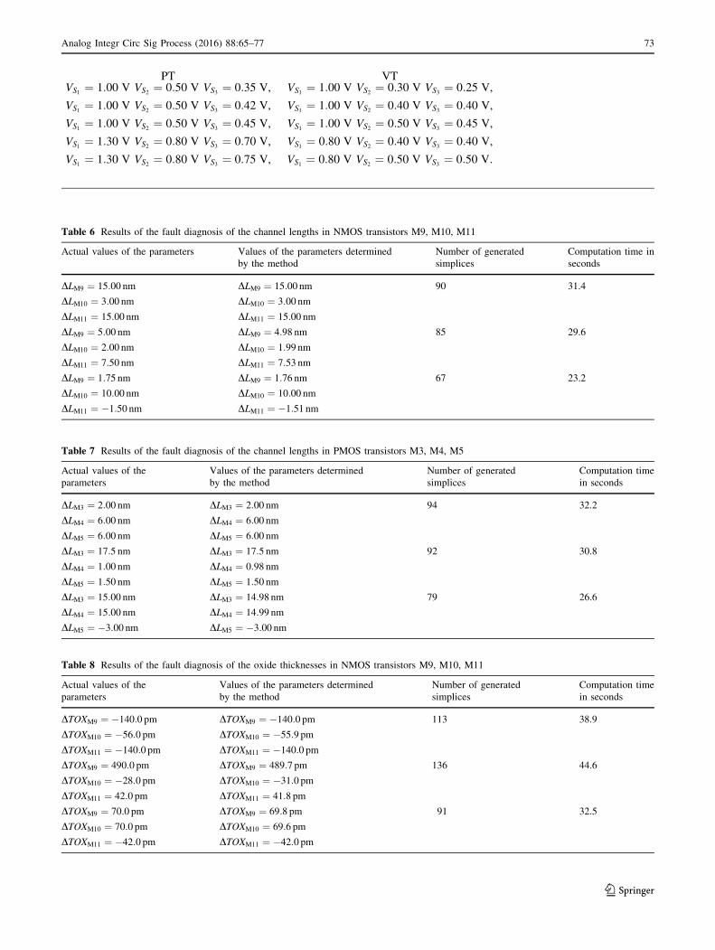
Table 6 Results of the fault diagnosis of the channel lengths in NMOS transistors M9, M10, M11
Actual values of the parameters Values of the parameters determined
by the method
Number of generated
simplices
Computation time in
seconds
DLM9 ¼ 15:00 nm
DLM10 ¼ 3:00 nm
DLM11 ¼ 15:00 nm
DLM9 ¼ 15:00 nm
DLM10 ¼ 3:00 nm
DLM11 ¼ 15:00 nm
90 31.4
DLM9 ¼ 5:00 nm
DLM10 ¼ 2:00 nm
DLM11 ¼ 7:50 nm
DLM9 ¼ 4:98 nm
DLM10 ¼ 1:99 nm
DLM11 ¼ 7:53 nm
85 29.6
DLM9 ¼ 1:75 nm
DLM10 ¼ 10:00 nm
DLM11 ¼ �1:50 nm
DLM9 ¼ 1:76 nm
DLM10 ¼ 10:00 nm
DLM11 ¼ �1:51 nm
67 23.2
Table 7 Results of the fault diagnosis of the channel lengths in PMOS transistors M3, M4, M5
Actual values of the
parameters
Values of the parameters determined
by the method
Number of generated
simplices
Computation time
in seconds
DLM3 ¼ 2:00 nm
DLM4 ¼ 6:00 nm
DLM5 ¼ 6:00 nm
DLM3 ¼ 2:00 nm
DLM4 ¼ 6:00 nm
DLM5 ¼ 6:00 nm
94 32.2
DLM3 ¼ 17:5 nm
DLM4 ¼ 1:00 nm
DLM5 ¼ 1:50 nm
DLM3 ¼ 17:5 nm
DLM4 ¼ 0:98 nm
DLM5 ¼ 1:50 nm
92 30.8
DLM3 ¼ 15:00 nm
DLM4 ¼ 15:00 nm
DLM5 ¼ �3:00 nm
DLM3 ¼ 14:98 nm
DLM4 ¼ 14:99 nm
DLM5 ¼ �3:00 nm
79 26.6
Table 8 Results of the fault diagnosis of the oxide thicknesses in NMOS transistors M9, M10, M11
Actual values of the
parameters
Values of the parameters determined
by the method
Number of generated
simplices
Computation time
in seconds
DTOXM9 ¼ �140:0 pm
DTOXM10 ¼ �56:0 pm
DTOXM11 ¼ �140:0 pm
DTOXM9 ¼ �140:0 pm
DTOXM10 ¼ �55:9 pm
DTOXM11 ¼ �140:0 pm
113 38.9
DTOXM9 ¼ 490:0 pm
DTOXM10 ¼ �28:0 pm
DTOXM11 ¼ 42:0 pm
DTOXM9 ¼ 489:7 pm
DTOXM10 ¼ �31:0 pm
DTOXM11 ¼ 41:8 pm
136 44.6
DTOXM9 ¼ 70:0 pm
DTOXM10 ¼ 70:0 pm
DTOXM11 ¼ �42:0 pm
DTOXM9 ¼ 69:8 pm
DTOXM10 ¼ 69:6 pm
DTOXM11 ¼ �42:0 pm
91 32.5
PT VTVS1
¼ 1:00 V VS2¼ 0:50 V VS3
¼ 0:35 V,
VS1¼ 1:00 V VS2
¼ 0:50 V VS3¼ 0:42 V,
VS1¼ 1:00 V VS2
¼ 0:50 V VS3¼ 0:45 V,
VS1¼ 1:30 V VS2
¼ 0:80 V VS3¼ 0:70 V,
VS1¼ 1:30 V VS2
¼ 0:80 V VS3¼ 0:75 V,
VS1¼ 1:00 V VS2
¼ 0:30 V VS3¼ 0:25 V,
VS1¼ 1:00 V VS2
¼ 0:40 V VS3¼ 0:40 V,
VS1¼ 1:00 V VS2
¼ 0:50 V VS3¼ 0:45 V,
VS1¼ 0:80 V VS2
¼ 0:40 V VS3¼ 0:40 V,
VS1¼ 0:80 V VS2
¼ 0:50 V VS3¼ 0:50 V:
Analog Integr Circ Sig Process (2016) 88:65–77 73
123
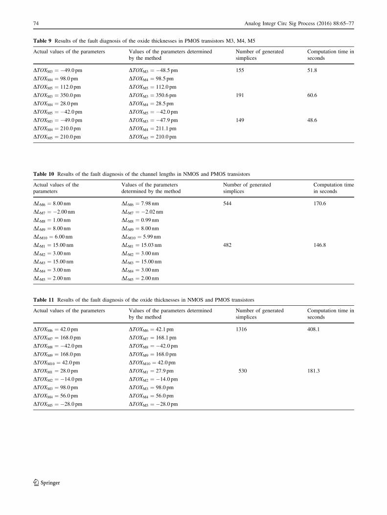
Table 9 Results of the fault diagnosis of the oxide thicknesses in PMOS transistors M3, M4, M5
Actual values of the parameters Values of the parameters determined
by the method
Number of generated
simplices
Computation time in
seconds
DTOXM3 ¼ �49:0 pm
DTOXM4 ¼ 98:0 pm
DTOXM5 ¼ 112:0 pm
DTOXM3 ¼ �48:5 pm
DTOXM4 ¼ 98:5 pm
DTOXM5 ¼ 112:0 pm
155 51.8
DTOXM3 ¼ 350:0 pm
DTOXM4 ¼ 28:0 pm
DTOXM5 ¼ �42:0 pm
DTOXM3 ¼ 350:6 pm
DTOXM4 ¼ 28:5 pm
DTOXM5 ¼ �42:0 pm
191 60.6
DTOXM3 ¼ �49:0 pm
DTOXM4 ¼ 210:0 pm
DTOXM5 ¼ 210:0 pm
DTOXM3 ¼ �47:9 pm
DTOXM4 ¼ 211:1 pm
DTOXM5 ¼ 210:0 pm
149 48.6
Table 10 Results of the fault diagnosis of the channel lengths in NMOS and PMOS transistors
Actual values of the
parameters
Values of the parameters
determined by the method
Number of generated
simplices
Computation time
in seconds
DLM6 ¼ 8:00 nm
DLM7 ¼ �2:00 nm
DLM8 ¼ 1:00 nm
DLM9 ¼ 8:00 nm
DLM10 ¼ 6:00 nm
DLM6 ¼ 7:98 nm
DLM7 ¼ �2:02 nm
DLM8 ¼ 0:99 nm
DLM9 ¼ 8:00 nm
DLM10 ¼ 5:99 nm
544 170.6
DLM1 ¼ 15:00 nm
DLM2 ¼ 3:00 nm
DLM3 ¼ 15:00 nm
DLM4 ¼ 3:00 nm
DLM5 ¼ 2:00 nm
DLM1 ¼ 15:03 nm
DLM2 ¼ 3:00 nm
DLM3 ¼ 15:00 nm
DLM4 ¼ 3:00 nm
DLM5 ¼ 2:00 nm
482 146.8
Table 11 Results of the fault diagnosis of the oxide thicknesses in NMOS and PMOS transistors
Actual values of the parameters Values of the parameters determined
by the method
Number of generated
simplices
Computation time in
seconds
DTOXM6 ¼ 42:0 pm
DTOXM7 ¼ 168:0 pm
DTOXM8 ¼ �42:0 pm
DTOXM9 ¼ 168:0 pm
DTOXM10 ¼ 42:0 pm
DTOXM6 ¼ 42:1 pm
DTOXM7 ¼ 168:1 pm
DTOXM8 ¼ �42:0 pm
DTOXM9 ¼ 168:0 pm
DTOXM10 ¼ 42:0 pm
1316 408.1
DTOXM1 ¼ 28:0 pm
DTOXM2 ¼ �14:0 pm
DTOXM3 ¼ 98:0 pm
DTOXM4 ¼ 56:0 pm
DTOXM5 ¼ �28:0 pm
DTOXM1 ¼ 27:9 pm
DTOXM2 ¼ �14:0 pm
DTOXM3 ¼ 98:0 pm
DTOXM4 ¼ 56:0 pm
DTOXM5 ¼ �28:0 pm
530 181.3
74 Analog Integr Circ Sig Process (2016) 88:65–77
123

Table 12 Results of the fault diagnosis of the channel lengths in NMOS transistors M4, M5, M8, M9 given by method M2014
Actual values of the parameters Values of the parameters
determined by the method
Computation time
in seconds
DLM4 ¼ 6:00 nm
DLM5 ¼ 4:00 nm
DLM8 ¼ 2:50 nm
DLM9 ¼ 6:00 nm
DLM4 ¼ 5:99 nm
DLM5 ¼ 3:99 nm
DLM8 ¼ 2:50 nm
DLM9 ¼ 6:02 nm
178.2
DLM4 ¼ 15:00 nm
DLM5 ¼ 2:00 nm
DLM8 ¼ 15:00 nm
DLM9 ¼ 4:50 nm
DLM4 ¼ 15:02 nm
DLM5 ¼ 1:98 nm
DLM8 ¼ 15:04 nm
DLM9 ¼ 4:53 nm
180.3
DLM4 ¼ 2:50 nm
DLM5 ¼ 2:00 nm
DLM8 ¼ 1:75 nm
DLM9 ¼ 20:00 nm
DLM4 ¼ 2:47 nm
DLM5 ¼ 1:96 nm
DLM8 ¼ 1:76 nm
DLM9 ¼ 20:06 nm
183.8
Table 13 Results of the fault diagnosis of the channel lengths in PMOS transistors M1, M2, M3 given by method M2014
Actual values of the parameters Values of the parameters
determined by the method
Computation time
in seconds
DLM1 ¼ 4:50 nm
DLM2 ¼ 3:00 nm
DLM3 ¼ 1:00 nm
DLM1 ¼ 4:57 nm
DLM2 ¼ 3:05 nm
DLM3 ¼ 1:01 nm
172.7
DLM1 ¼ 15:00 nm
DLM2 ¼ 10:00 nm
DLM3 ¼ 2:50 nm
DLM1 ¼ 15:01 nm
DLM2 ¼ 9:99 nm
DLM3 ¼ 2:51 nm
178.4
DLM1 ¼ 1:50 nm
DLM2 ¼ 25:00 nm
DLM3 ¼ 1:00 nm
DLM1 ¼ 1:46 nm
DLM2 ¼ 25:03 nm
DLM3 ¼ 1:00 nm
171.2
Table 14 Results of the fault diagnosis of the oxide thicknesses in NMOS transistors M4, M5, M8, M9 given by method M2014
Actual values of the parameters Values of the parameters determined
by the method
Computation time in seconds
DTOXM4 ¼ 140:0 pm
DTOXM5 ¼ �56:0 pm
DTOXM8 ¼ �28:0 pm
DTOXM9 ¼ 98:0 pm
DTOXM4 ¼ 141:3 pm
DTOXM5 ¼ �55:6 pm
DTOXM8 ¼ �26:9 pm
DTOXM9 ¼ 97:9 pm
190.2
DTOXM4 ¼ 280:0 pm
DTOXM5 ¼ �56:0 pm
DTOXM8 ¼ 280:0 pm
DTOXM9 ¼ �42:0 pm
DTOXM4 ¼ 281:4 pm
DTOXM5 ¼ �59:2 pm
DTOXM8 ¼ 282:7 pm
DTOXM9 ¼ �40:7 pm
158.6
DTOXM4 ¼ 70:0 pm
DTOXM5 ¼ �56:0 pm
DTOXM8 ¼ �49:0 pm
DTOXM9 ¼ 560:0 pm
DTOXM4 ¼ 70:8 pm
DTOXM5 ¼ �56:0 pm
DTOXM8 ¼ �48:1 pm
DTOXM9 ¼ 559:1 pm
179.5
Analog Integr Circ Sig Process (2016) 88:65–77 75
123
Some results of multiple soft fault diagnosis are sum-
marized in Tables 10, 11. The obtained values of the
parameters are very close to their actual values.
6 Conclusion
The method developed in this paper allows effective
diagnosing multiple soft faults of the process parameters in
small and middle–size ICs designed in nanometer tech-
nology. The method does not require access to internal
nodes of the circuit. The set of the parameter values is
obtained by solving nonlinear equations, not given in
explicit analytical form, that may have more than one
solution. The proposed approach, whose core is the
Nelder–Mead optimization method, is capable of finding
the multiple solutions and select the actual one. Numerical
examples reveal that the accuracy of the determined
parameter values is very good. The method does not allow
testing the transistors whose parameters have slight influ-
ence on the output voltage. This is why the fault diagnosis
process should be preceded by the sensitivity analyses.
The proposed method has been compared with the
methods recently published in references [18] and [20]
devoted to similar problem. They will be named M2016,
M2014 and M2015, respectively.
At first we concentrate on the methods M2016 and M2014.
To perform the comparison, method M2014 has been imple-
mented to allow diagnosing CMOS circuits designed in
nanometer technology, comprising the transistors character-
ized by the model BSIM 4.6. All 30 fault diagnoses included in
Tables 1, 2, 3, 4, 5, 6, 7, 8, 9, 10, 11 providing the results found
by method M2016, have been performed using method
M2014 with the same diagnostic tests and the assumed mea-
surement accuracy and the parameters /, n, kmax as in [18]
(Example 1). On the basis of these experiments the following
conclusion can be drawn. Method M2014 is very sensitive to
the tests and in numerous cases several tries must be taken to
select the proper one. Moreover, sometimes this method
requires more than one measurement node. In the great
majority of cases method M2014 is more time consuming than
method M2016. To be specific, let us consider in detail
Example 1. For the diagnoses included in Tables 1, 2, 3 the
results given by method M2014 are very similar to the ones
provided by method M2016 (see Tables 12, 13, 14). In all
cases, except one, method M2014 consumes more CPU time
which is 1.48–6.64 times longer. For the cases presented in
Tables 4, 5 method M2014 fails. However, it is possible to
arrange another tests so that the method works and gives
correct results. Unfortunately, the tests relating to the diag-
noses indicated in Table 5 requires access to two measure-
ment nodes.
Method M2015 comprises very large class of circuits,
including bipolar and CMOS ones, designed in micrometer
and submicrometer technologies. In Ref. [20] the MOS
transistors designed in nanometer technology are charac-
terized by PSP103.1 model introduced into DELPHI
environment. Thanks to this the circuit analyses are exe-
cuted using a dedicated program written in DELPHI, that
considerably improves the computation process and makes
the method sound. To compare with M2016 the method
M2015 was implemented including BSIM 4.6 modeled
MOS transistors and circuit analyses were performed in
IsSPICE 4. Method M2015 requires numerous sensitivity
analyses that in this case must be performed using the
brute–force incremental approach. In consequence this
method needs large computing power and consumes much
CPU time. Thus, method M2016 is less universal than
M2015 but, in the case of CMOS circuits with BSIM 4.6
modeled transistors, faster and easier to implement. To be
specific, all the cases presented in Tables 1, 2, 3, 4 were
retaken using method M2015 with h ¼ 0:05. The method
gives the results very close to the ones provided by M2016,
but the CPU time is 7–45 times longer.
Open Access This article is distributed under the terms of the
Creative Commons Attribution 4.0 International License (http://crea
tivecommons.org/licenses/by/4.0/), which permits unrestricted use,
distribution, and reproduction in any medium, provided you give
appropriate credit to the original author(s) and the source, provide a
link to the Creative Commons license, and indicate if changes were
made.
References
1. Aminian, M., & Aminian, F. (2007). A modular fault-diagnostic
system for analog electronic circuits using neural networks with
wavelet transform as a preprocessor. IEEE Transactions on
Instrumentation and Measurement, 56, 1546–1554.
2. Bhunia, S., Raychowdhury, A., & Roy, K. (2005). Defect oriented
testing of analog circuits using wavelet analysis of dynamic supply
current. Journal of Electronic Testing, 21, 147–159.
3. Catelani, M., & Fort, A. (2002). Soft fault detection and isolation
in analog circuits: some results and a comparison between a fuzzy
approach and radial basis function networks. IEEE Transactions
on Instrumentation and Measurement, 51, 196–202.
4. Economikos, L., Morrison, T., & Crnic, F. (1994). Electrical test
of multichip substrates. IEEE Transactions on Components,
Packaging, and Manufacturing Technology, Part B: Advanced
Packaging, 17, 56–61.
5. Fedi, G., Giomi, R., Luchetta, A., Manetti, S., & Piccirilli, M. C.
(1998). On the application of symbolic techniques to the multiple
fault location in low testability analog circuits. IEEE Transac-
tions on Circuits and Systems II: Analog and Digital Signal
Processing, 45, 1383–1388.
6. Gizopoulos, D. (Ed.). (2006). Advances in electronic testing:
Challenges and methodologies. Dordrecht: Springer.
7. Huang, K., Stratigopoulos, H. G., Mir, S., Hora, C., Xing, Y., &
Kruseman, B. (2012). Diagnosis of local spot defect in analog
circuits. IEEE Transactions on Instrumentation and Measure-
ment, 61, 2701–2712.
76 Analog Integr Circ Sig Process (2016) 88:65–77
123

8. Jahangiri, M., & Razaghian, F. (2014). Fault detection in ana-
logue circuits using hybrid evolutionary algorithm and neural
network. Analog Integrated Circuits and Signal Processing,
80(3), 551–556.
9. Kabisatpathy, P., Barua, A., & Sinha, S. (2005). Fault diagnosis
of analog integrated circuits. Dordrecht: Springer.
10. Kim, B., Swaminathan, M., Chatterjee, A., & Schimmel, D.
(1997). A novel test technique for MCM substrates. IEEE
Transactions on Components, Packaging, and Manufacturing
Technology, Part B: Advanced Packaging, 20, 2–12.
11. Papakostas, D. K., & Hatzopoulos, A. A. (2008). A unified pro-
cedure for fault detection of analog and mixed-mode circuits
using magnitude and phase components of the power supply
current spectrum. IEEE Transactions on Instrumentation and
Measurement, 57, 2589–2995.
12. Provost, B., & Sanchez-Sinencio, E. (2003). On-chip ramp gen-
erators for mixed-signal BIST and ADC self-test. IEEE Journal
of Solid-State Circuits, 38(2), 263–273.
13. Robotycki, A., & Zielonko, R. (2002). Fault diagnosis of analog
piecewise linear circuits based on homotopy. IEEE Transactions
on Instrumentation and Measurement, 51, 876–881.
14. Segura, J., Keshavarzi, A, Soden, J, & Hawkins, C. (2002).
Parametric failures in CMOS ICs—a defect-based analysis. In
Proceedings of the International Test Conference (pp.90–99).
15. Sunter, S., & Nagi, N. (1999). Test metrics for analog parametric
faults. In Proceedings of the 17th IEEE VLSI Test Symposium
(pp.226–234).
16. Tadeusiewicz, M., Hałgas, S., & Korzybski, M. (2002). An
algorithm for soft-fault diagnosis of linear and nonlinear circuits.
IEEE Transactions on Circuits and Systems I: Fundamental
Theory and Applications, 49, 1648–1653.
17. Tadeusiewicz, M., & Hałgas, S. (2012). Multiple soft fault diag-
nosis of nonlinear circuits using the continuation method. Journal
of Electronic Testing: Theory and Applications, 28, 487–493.
18. Tadeusiewicz, M., & Hałgas, S. (2014). Global and local para-
metric diagnosis of analog short-channel CMOS circuit using
homotopy-simplicial algorithm. International Journal of Circuit
Theory and Applications, 42, 1051–1068.
19. Tadeusiewicz, M., & Hałgas, S. (2014). Multiple soft fault diagnosis
of BJT circuit. Metrology and Measurement Systems, 21, 663–674.
20. Tadeusiewicz, M., & Hałgas, S. (2015). A new approach to
multiple soft fault diagnosis of analog BJT and CMOS circuits.
IEEE Transactions on Instrumentation and Measurement, 64,
2688–2695.
21. Tadeusiewicz, M., Kuczynski, A., & Hałgas, S. (2015). Spot
defect diagnosis in analog nonlinear circuits with possible mul-
tiple operating points. Journal of Electronic Testing: Theory and
Applications, 31, 491–502.
22. Wang, Z., Gielen, G., & Sansen, W. (1998). Probabilistic fault
detection and the selection of measurements for analog integrated
circuits. IEEE Transactions on Computer-Aided Design of Inte-
grated Circuits and Systems, 17(9), 862–872.
23. Singer, S., & Nelder, J. (2009). Nelder–Mead algorithm. Schol-
arpedia, 4(7), 2928.
24. Luersen, M. A., & Le Riche, R. (2004). Globalized Nelder–Mead
method for engineering optimization. Computers & Structures,
82, 2251–2260.
25. Gao, F., & Han, L. (2012). Implementing the Nelder–Mead
simplex algorithm with adaptive parameters. Computational
Optimization and Applications., 51, 259–277.
26. IsSPICE4 User’s Guide, vol.1,2, rev. 04/08 Build 3247, Intusoft
2008.
27. Baker, R. J. (2010). CMOS circuit design, layout, and simulation.
New York: Wiley-IEEE Press.
Michał Tadeusiewicz Ph.D.,
D.Sc. Professor graduated from
Lodz University of Technology,
Poland, in Electronic and Elec-
trical Engineering. Prof. Tadeu-
siewicz is a full professor in the
Department of Electrical, Elec-
tronic, Computer, and Control
Engineering, Lodz, University
of Technology. His research
interests include theory and
analysis of nonlinear circuits
and fault diagnosis of analog
circuits. He is the author and
coauthor of 195 technical
papers, two books, and 15 textbooks.
Stanisław Hałgas Ph.D., D.Sc.
graduated from Lodz University
of Technology, Poland, in
Electronic and Electrical Engi-
neering. Dr Hałgas is a associate
professor in the Department of
Electrical, Electronic, Com-
puter, and Control Engineering,
Lodz University of Technology,
and head of Nonlinear Circuits
and Systems Division. His
research interests are in the
areas of nonlinear circuits anal-
ysis and fault diagnosis of ana-
log circuits. He is the author or
coauthor of one monograph, one textbook, and 100 technical papers.
Analog Integr Circ Sig Process (2016) 88:65–77 77
123