Multiple E-beam Direct Write REBL - WebHome -...
16
Multiple E-beam Direct Write & REBL Yasmine Badr
Transcript of Multiple E-beam Direct Write REBL - WebHome -...

Multiple E-beam Direct Write
&
REBL
Yasmine Badr
NanoCAD Lab
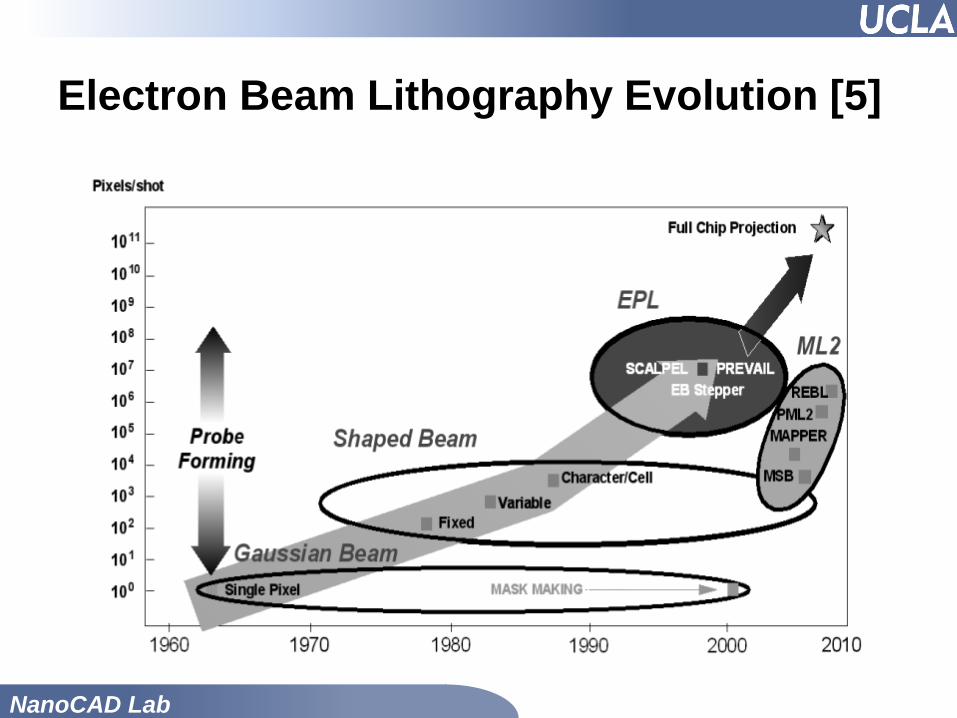
Electron Beam Lithography Evolution [5]

NanoCAD Lab
Motivation
“For the first time in half a century, electron-beam
lithography shows signs of living up to its promise of
manufacturing semiconductor circuits in high volume.”
--Burn Lin, TSMC, Taiwan
14 January 2013, SPIE Newsroom
NanoCAD Lab
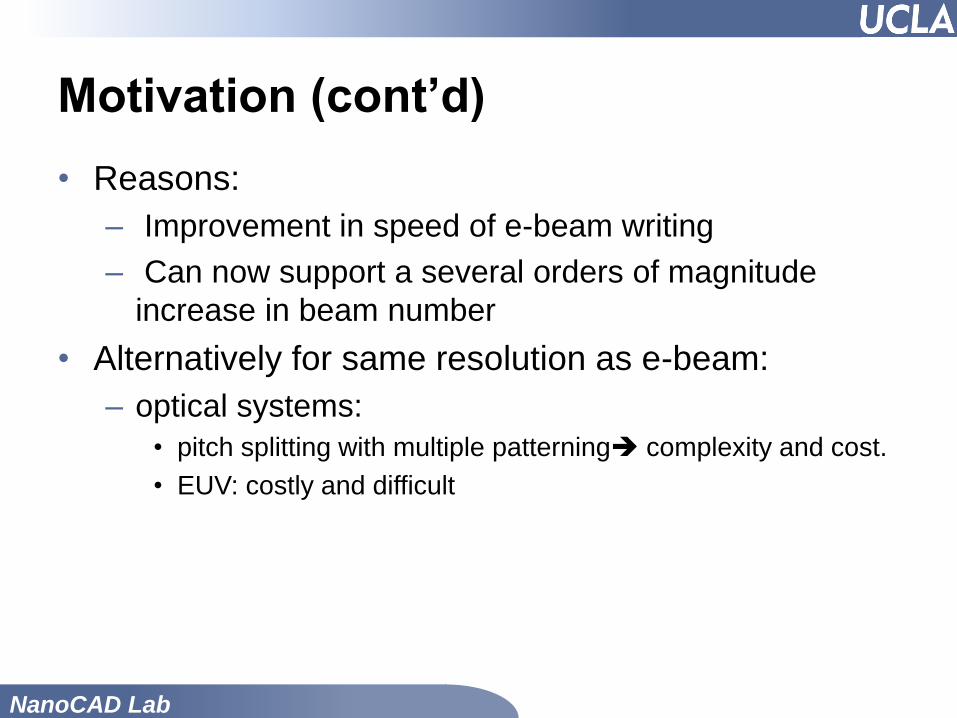
Motivation (cont’d)
• Reasons:
– Improvement in speed of e-beam writing
– Can now support a several orders of magnitude
increase in beam number
• Alternatively for same resolution as e-beam:
– optical systems:
• pitch splitting with multiple patterning complexity and cost.
• EUV: costly and difficult

NanoCAD Lab
E-beam
+ Resolution
+ Depth of Focus
– Ebeam: DoF> 1um with 10% exposure latitude.
– Optical systems: DoF <100nm.
+ No mask
-Throughput
NanoCAD Lab
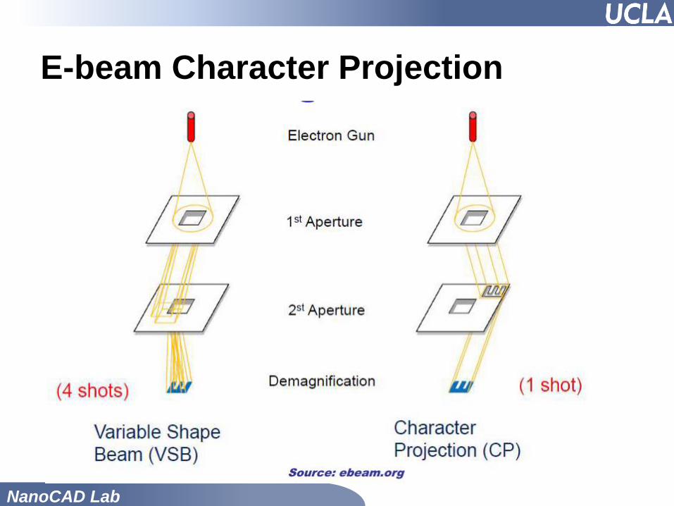
E-beam Character Projection

NanoCAD Lab
Design for E-beam: Character Projection
[4]
• Co-design of the standard cell library with the stencil
mask
– once per library
– 10-20X speedups in e-beam

NanoCAD Lab
Reflective Electron Beam Lithography
(REBL) [2]
• By KLA-Tencor
• Target:16nm
• Throughput target: 100 wph

NanoCAD Lab
Reflective Electron Beam Lithography
(REBEL) [2]
• uses a reflective
dynamic pattern
generator (DPG)
– to modulate the aerial
image of a large area
electron beam
NanoCAD Lab
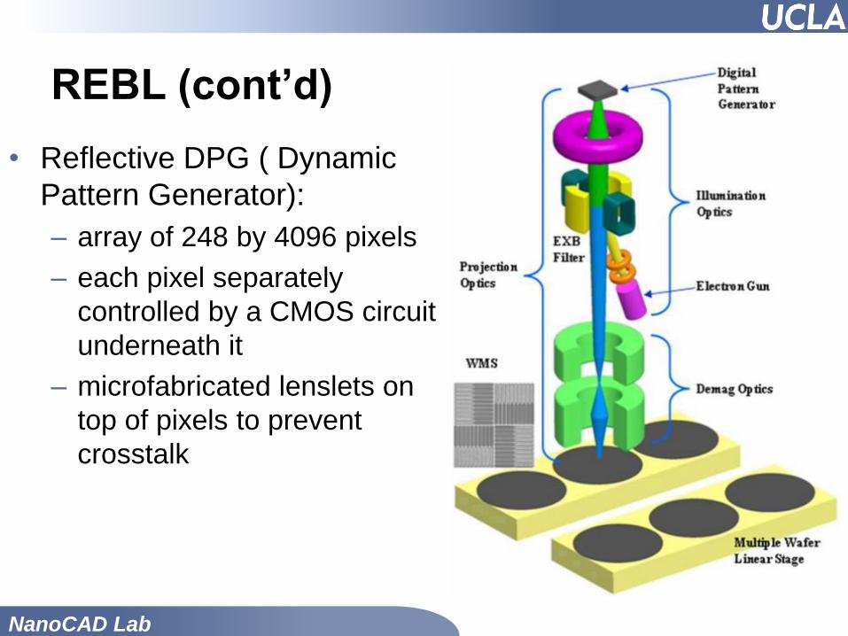
REBL (cont’d)
• Reflective DPG ( Dynamic
Pattern Generator):
– array of 248 by 4096 pixels
– each pixel separately
controlled by a CMOS circuit
underneath it
– microfabricated lenslets on
top of pixels to prevent
crosstalk

NanoCAD Lab
REBL (cont’d)
• Reflective DPG ( Dynamic
Pattern Generator):
– By switching voltage (2v) of
electrode of pixel, electrons
from electron gun can be
either :
• reflected back into projection
optics (“on” pixel) or
• absorbed by electrode (“off”
pixel).

NanoCAD Lab
REBL (cont’d)
• EXB: electromagnetic filter
• Projection optics:
– demagnify DPG image by
100X onto moving stage.
• WMS: Wafer metrology site
– Optically measures wafer
position
NanoCAD Lab
Mask Data Preparation
• Proximity Correction using LP [6]
– Minimize total exposure time
– Subject to :
• all required pixels receive above-threshold dose and
• non-required pixels receive below-threshold dose

NanoCAD Lab
Rendering Data
• Render the data: convert it into pixels with gray level
assignments.
– Use proximity corrected data
• Converted pattern sent for writing
• Gray level pixel data distributed to each DPG during
the writing process
NanoCAD Lab
Multiple beams in REBL
• As many as 36 columns can be clustered on either a
rotary stage or six linear stages.
– However seems like their current only uses one
column
• Performance target: 100 wph [2]

NanoCAD Lab
References
[1] Burn Lin; “Multiple-electron-beam direct-write comes of age”; SPIE
Newsroom, Jan 2013
[2] McCord, M. A.; Petric, P.; Ummethala, U.; Carroll, A.; Kojima, S.; Grella, L.;
Shriyan, S.; Rettner, C. T. & Bevis, C. F.; “REBL: design progress toward 16 nm
half-pitch maskless projection electron beam lithography”,Proc. SPIE, 2012
[3] McCord, M. A.; Petric, P.; Ummethala, U.; Carroll, A.; Kojima, S.; Grella, L.;
Shriyan, S.; Rettner, C. T. & Bevis, C. F.; “REBL: design progress toward 16 nm
half-pitch maskless projection electron beam lithography”, 2012
[4] Fujimura, A.; “Design for e-beam: design insights for direct-write maskless
lithography”; SPIE Photomask Technology, 2010
[5] Pfeiffer, H. C.; “Direct write electron beam lithography: a historical overview”
Proc. of SPIE Vol, 2010
[6] Carroll, A. M.Proximity-effect correction with linear programming; Journal of
Applied Physics, AIP, 1981