
Multimode (LVD/SE) SCSI 9 Line Terminator datasheet (Rev. B)
13
UCC5672 SLUS414B - FEBRUARY 2000 - REVISED MARCH 2002 FEATURES • Auto Selection Multi-Mode Single Ended or Low Voltage Differential Termination • 2.7V to 5.25V Operation • Differential Failsafe Bias • Built-in SPI-3 Mode Change Filter/ Delay • Meets SCSI-1, SCSI-2, Ultra2 (SPI-2 LVD), Ultra3/Ultra160 (SPI-3) and Ultra320 (SPI-4) Standards • Supports Active Negation • 3pF Channel Capacitance Multimode (LVD/SE) SCSI 9 Line Terminator 1 27 16 DIFSENS DIFSENS REF 1.3V ENABLE 3 L1– 52 2 L1+ 52 L9– L9+ 56mV + – 56mV – + 124 110 SE GROUND SWITCH 26 52 25 52 56mV + – 56mV – + 124 110 SE GROUND SWITCH REG 17 DIFFB 0.6V 2.1V FILTER/ DELAY 28 TRMPWR TRMPWR LVD REF 1.25V SOURCE/SINK REGULATORS SE REF 2.7V ENABLE SW1 10µA 22 6 HS/GND HS/GND 14 GND 13 DISCNCT SE DISCNCT HPD LVD UP OPEN DOWN DOWN DOWN UP OPEN OPEN MODE SW1 OTHER SWITCHES HPD LVD SE BLOCK DIAGRAM UDG-99125 DESCRIPTION The UCC5672 Multi-Mode Low Voltage Differential and Single Ended Ter- minator is both a single ended terminator and a low voltage differential ter- minator for the transition to the next generation SCSI Parallel Interface (SPI-3). The low voltage differential is a requirement for the higher speeds at a reasonable cost and is the only way to have adequate skew budgets. The automatic mode select/change feature switches the terminator be- tween Single Ended or LVD SCSI Termination, depending on the bus mode. If the bus is in High Voltage Differential Mode, the terminator lines transition into a High Impedance state. The UCC5672 is SPI-4, SPI-3, SPI-2, and SCSI-2 compliant. This device is offered in a 28 pin TSSOP package to minimize the footprint. The UCC5672 is also available in a 36 pin MWP package. Note: Indicated pinout is for 28 pin TSSOP package.
Transcript of Multimode (LVD/SE) SCSI 9 Line Terminator datasheet (Rev. B)

UCC5672
SLUS414B - FEBRUARY 2000 - REVISED MARCH 2002
FEATURES• Auto Selection Multi-Mode Single
Ended or Low Voltage DifferentialTermination
• 2.7V to 5.25V Operation
• Differential Failsafe Bias
• Built-in SPI-3 Mode Change Filter/Delay
• Meets SCSI-1, SCSI-2, Ultra2 (SPI-2LVD), Ultra3/Ultra160 (SPI-3) andUltra320 (SPI-4) Standards
• Supports Active Negation
• 3pF Channel Capacitance
Multimode (LVD/SE) SCSI 9 Line Terminator
1
27
16 DIFSENSDIFSENSREF 1.3V
ENABLE
3 L1–52
2 L1+52
L9–
L9+
56mV+ –
56mV– +
124
110
SE GROUNDSWITCH
2652
255256mV
+ –
56mV– +
124
110
SE GROUNDSWITCH
REG
17DIFFB
0.6V
2.1V
FILTER/DELAY
28TRMPWR
TRMPWR
LVD REF1.25V
SOURCE/SINKREGULATORS
SE REF2.7V
ENABLE
SW1
10µA
22
6HS/GND
HS/GND
14GND
13DISCNCT
SE
DISCNCTHPDLVD
UP
OPENDOWNDOWN DOWN
UP
OPENOPEN
MODE SW1OTHERSWITCHES
HPD
LVD
SE
BLOCK DIAGRAM
UDG-99125
DESCRIPTIONThe UCC5672 Multi-Mode Low Voltage Differential and Single Ended Ter-minator is both a single ended terminator and a low voltage differential ter-minator for the transition to the next generation SCSI Parallel Interface(SPI-3). The low voltage differential is a requirement for the higher speedsat a reasonable cost and is the only way to have adequate skew budgets.
The automatic mode select/change feature switches the terminator be-tween Single Ended or LVD SCSI Termination, depending on the busmode. If the bus is in High Voltage Differential Mode, the terminator linestransition into a High Impedance state.
The UCC5672 is SPI-4, SPI-3, SPI-2, and SCSI-2 compliant. This deviceis offered in a 28 pin TSSOP package to minimize the footprint. TheUCC5672 is also available in a 36 pin MWP package.
Note: Indicated pinout is for 28 pin TSSOP package.
2
UCC5672
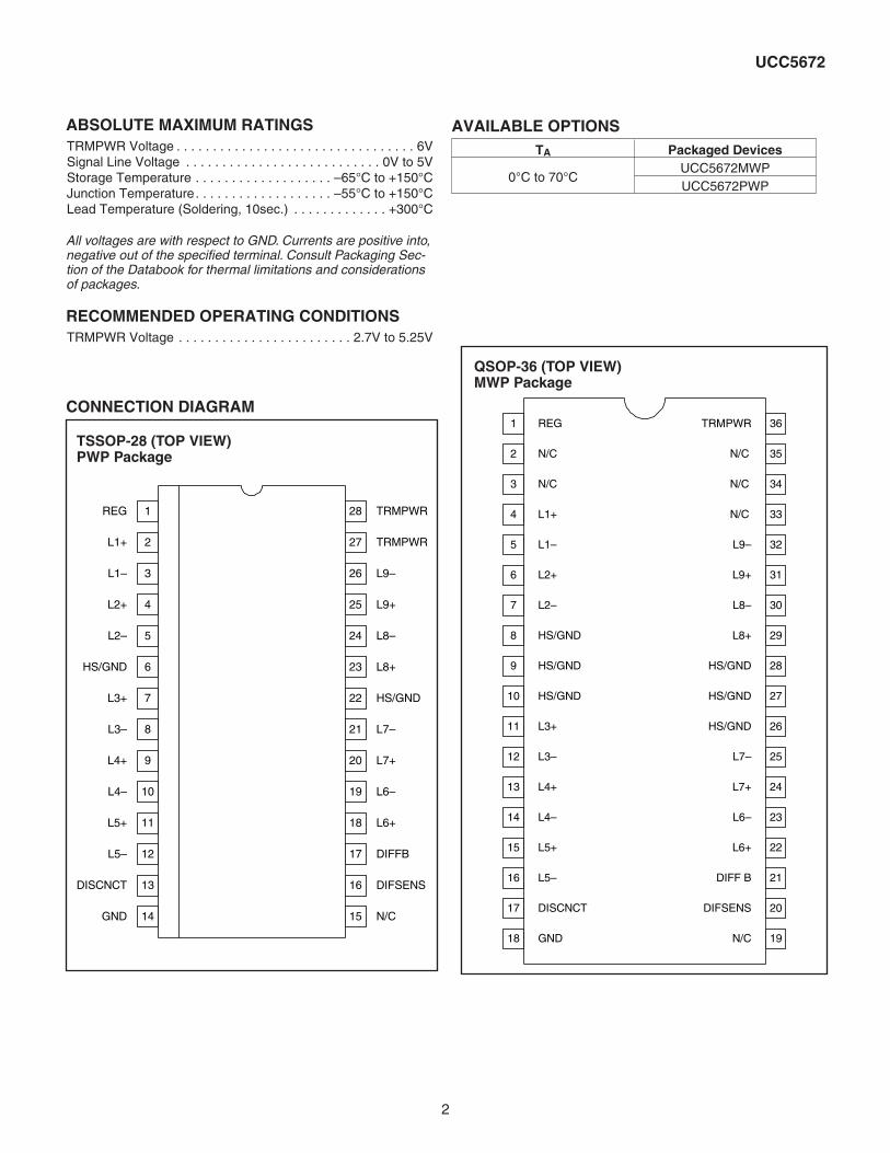
ABSOLUTE MAXIMUM RATINGSTRMPWR Voltage . . . . . . . . . . . . . . . . . . . . . . . . . . . . . . . . . 6VSignal Line Voltage . . . . . . . . . . . . . . . . . . . . . . . . . . . 0V to 5VStorage Temperature . . . . . . . . . . . . . . . . . . . –65°C to +150°CJunction Temperature. . . . . . . . . . . . . . . . . . . –55°C to +150°CLead Temperature (Soldering, 10sec.) . . . . . . . . . . . . . +300°C
All voltages are with respect to GND. Currents are positive into,negative out of the specified terminal. Consult Packaging Sec-tion of the Databook for thermal limitations and considerationsof packages.
RECOMMENDED OPERATING CONDITIONSTRMPWR Voltage . . . . . . . . . . . . . . . . . . . . . . . . 2.7V to 5.25V
DIFFB
L6+
L8–
L8+
L7–
TRMPWR
L1+
L4–
L3+
L4+
L1–
L2+
L2–
REG
L3–
DIFSENS
L7+
L6–
L5+
GND 14
13
12
11
10
9
8
7
6
5
4
3
2
1
15
16
17
18
19
20
21
22
23
24
25
26
27
28
L5–
N/C
DISCNCT
L9–
L9+
TRMPWR
HS/GND
HS/GND
CONNECTION DIAGRAM
L3+
HS/GND
L9–
L9+
L8–
TRMPWR
N/C
N/C
HS/GND
L2–
HS/GND
L1+
L1–
L2+
REG
HS/GND
L3–
L8+
HS/GND
HS/GND
L4+
L4–14
13
12
11
10
9
8
7
6
5
4
3
2
1
23
24
25
26
27
28
29
30
31
32
33
34
35
36
18
17
16
15
DIFF B
N/C
DIFSENS
19
20
21
22L5+
L5–
DISCNCT
GND
L7–
L7+
L6–
L6+
N/C
N/C
N/C
TSSOP-28 (TOP VIEW)PWP Package
QSOP-36 (TOP VIEW)MWP Package
TA Packaged Devices
0 C to 70°CUCC5672MWPUCC5672PWP
AVAILABLE OPTIONS

3
UCC5672
ELECTRICAL CHARACTERISTICS Unless otherwise stated, these specifications apply for TA = TJ = 0°C to 70°C,TRMPWR = 2.7V to 5.25V.
PARAMETER TEST CONDITIONS MIN TYP MAX UNITS
TRMPWR Supply Current Section
TRMPWR Supply Current LVD SCSI Mode 23 35 mA
SE Mode 14 25 mA
DISCNCT Mode 250 500 µA
Regulator Section
1.25V Regulator Output Voltage LVD SCSI Mode 1.15 1.25 1.35 V
1.25V Regulator Source Current VREG= 0V –225 –420 –800 mA
1.25V Regulator Sink Current VREG= 3.3V 100 180 420 mA
2.7V Regulator Output Voltage SE Mode 2.5 2.7 3.0 V
2.7V Regulator Source Current VREG= 0V –225 –420 –800 mA
2.7V Regulator Sink Current VREG= 3.3V 100 180 420 mA
Diff Sense Driver (DIFSENS) Section
1.3V DIFSENS Output Voltage DIFSENS 1.2 1.3 1.4 V
1.3V DIFSENS Source Current VDIFSENS = 0V –5 –15 mA
1.3V DIFSENS Sink Current VDIFSENS = 2.75V 50 200 µA
Differential Termination Section
Differential Impedance 100 105 110 ΩCommon Mode Impedance (Note 2) 110 150 165 ΩDifferential Bias Voltage 100 125 mV
Common Mode Bias 1.15 1.25 1.35 V
Output Capacitance Single Ended Measurement to Ground (Note 1) 3 pF
Single Ended Termination Section
ImpedanceZ VL V
ILX
X= −( . )0 2 , (Note 3)
100 108 116 Ω
Termination Current Signal Level 0.2V, All Lines Low –20 –23 –25.4 mA
Signal Level 0.5V –17 –22.4 mA
Output Leakage 400 nA
Output Capacitance Single Ended Measurement to Ground (Note 1) 3 pF
Single Ended GND SE Impedance I= 10mA 20 60 ΩDisconnect (DISCNCT) and Diff Buffer (DIFFB) Input Section
DISCNCT Threshold 0.8 2.0 V
DISCNCT Input Current –10 –30 µA
DIFFB SE to LVD SCSI Threshold 0.5 0.7 V
DIFFB LVD SCSI to HPD Threshold 1.9 2.4 V
DIFFB Input Current –1 1 µA

4
UCC5672
ELECTRICAL CHARACTERISTICS Unless otherwise stated, these specifications apply for TA = TJ = 0°C to 70°C,TRMPWR = 2.7V to 5.25V.
PARAMETER TEST CONDITIONS MIN TYP MAX UNITS
Time Delay/Filter Section
Mode Change Delay A new mode change can start any time after aprevious mode change has been detected.(Note4 )
100 180 300 ms
Note 1: Guaranteed by design. Not 100% tested in production.
Note 2:( ) ( )
ZV
I ICMV V V VCM CM
=−+ −
1 2
0 6 0 6
.
. .
; Where VCM = Voltage measured with L+ tied to L– and zero current applied;
Note 3: VLX= Output voltage for each terminator minus output pin (L1– through L9–) with each pin unloaded.ILX = Output current for each terminator minus output pin (L1– through L9–) with the minus output pin forced to 0.2V.
Note 4: Noise on DIFFB will not cause a false mode change. The time delay is that same for a change from any mode to anyother mode. Within 300ms after power is applied the mode is defined by the voltage of DIFFB.
PIN DESCRIPTIONSDIFFB: Input pin for the comparators that select SE,LVD SCSI, or HIPD modes of operation. This pin shouldbe decoupled with a 0.1µF capacitor to ground and thencoupled to the DIFSENS pin through a 20kΩ resistor.
DIFSENS: Connects to the Diff Sense line of the SCSIbus. The bus mode is controlled by the voltage level onthis pin.
DISCNCT: Input pin used to shut down the terminator ifthe terminator is not connected at the end of the bus.Connect this pin to ground to activate the terminator oropen pin to disable the terminator.
HS/GND: Heat sink ground pins. These should be con-nected to large ground area PC board traces to increasethe power dissipation capability.
GND: Power Supply return.
L1– thru L9–: Termination lines. These are the activelines in SE mode and are the negative lines for LVDSCSI mode. In HIPD mode, these lines are high imped-ance.
L1+ thru L9+: Termination lines. These lines switch toground in SE mode and are the positive lines for LVDSCSI mode. In HIPD mode, these lines are high imped-ance.
REG: Regulator bypass pin, must be connected to a4.7µF capacitor to ground.
TRMPWR: 2.7V to 5.25V power input pin. Bypass nearthe terminators with a 4.7µF capacitor to ground.
All SCSI buses require a termination network at eachend to function properly. Specific termination require-ments differ, depending on which types of SCSI devicesare present on the bus.
The UCC5672 is used in multi-mode active terminationapplications, where single ended (SE) and low voltagedifferential (LVD) SCSI devices might coexist. TheUCC5672 has both SE and LVD SCSI termination net-works integrated into a single monolithic component. Thecorrect termination network is automatically determinedby the SCSI bus "DIFSENS" signal.
The SCSI bus DIFSENS signal line is used to identifywhich types of SCSI devices are present on the bus. Onpower-up, the UCC5672 DIFSENS drivers will try to de-
liver 1.3V to the DIFSENS line. If only LVD SCSI devicesare present, the DIFSENS line will be successfully drivento 1.3V and the terminators will configure for LVD SCSIoperation. If any single ended devices are present, theywill present a short to ground on the DIFSENS line, sig-naling the UCC5672(s) to configure into the SE mode,accommodating the SE devices. Or, if any high voltagedifferential (HVD) SCSI devices are present, theDIFSENS line is pulled high and the terminator will entera high impedance state, effectively disconnecting fromthe bus.
The DIFSENS line is monitored by each terminatorthrough a 50Hz noise filter at the DIFFB input pin. A setof comparators detect and select the appropriate termi-
APPLICATION INFORMATION

5
UCC5672
nation for the bus as follows. If the DIFSENS signal isbelow 0.5V, the termination network is set for singleended. Between 0.7V and 1.9V, the termination networkswitches to LVD SCSI, and above 2.4V indicates HVDSCSI, causing the terminators to disconnect from thebus. These thresholds accommodate differences inground potential that can occur with long lines.
Three UCC5672 multi-mode parts are required at eachend of the bus to terminate 27 (18 data, plus 9 control)lines. Each part includes a DIFSENS driver, but only oneis necessary to drive the line. The DIFFB inputs on allthree parts are connected together, allowing them toshare the same 50Hz noise filter. This multi-mode termi-nator operates in full specification down to 2.7VTRMPWR voltage. This accommodates 3.3V systems,
APPLICATION INFORMATION (cont.)
REG DIFFB
16
1 17
16
CONTROL LINES (9)
20 k20 k
DIFF SENSE
4 2
5 3
4.7 F0.1 µF
31 25
32 26
L1+
L1–
L9+
L9–
L1+
L1–
L9+
L9–
DIFFS
UCC5672 UCC5672
DIFFS
REGDIFFB
117
4.7 F0.1 µF
REG DIFFB
1 17
DATA LINES (9)
4 2
5 3
4.7 F
31 25
32 26
L1+
L1–
L9+
L9–
L1+
L1–
L9+
L9–
UCC5672 UCC5672
REGDIFFB
117
4.7 F
REG
TRMPWR
DIFFB
28
1 17
DATA LINES (9)
2 2
3 3
4.7 F
25 25
26 26
L1+
L1–
L9+
L9–
L1+
L1–
L9+
L9–
UCC5672 UCC5672
27 TRMPWR
13 DISCNCT
REGDIFFB
117
4.7 F
TRMPWR28
27 TRMPWR
13 DISCNCT
TRMPWR28
27 TRMPWR
13 DISCNCT
28
27
13
TRMPWR
TRMPWR
DISCNCT
28
27
13
TRMPWR
TRMPWR
DISCNCT
28
27
13
TRMPWR
TRMPWR
DISCNCT
16 NC
16 NCNC 16
NC 16
4.7 F4.7 F
Termpower Termpower
Figure 1. Application diagram.
Note: Indicated pinout is for 28 pin TSSOP package. UDG-99126

6
UCC5672
with allowance for the 3.3V supply tolerance (+/- 10%), aunidirectional fusing device and cable drop. In 3.3VTRMPWR systems, the UCC3918 is recommended inplace of the fuse and diode. The UCC3918's lower volt-age drop allows additional margin over the fuse and di-ode, for the far end terminator.
Layout is critical for Ultra2, Ultra3/Ultra160 and Ultra320systems. The SPI-2 standard for capacitance loading is10pF maximum from each positive and negative signalline to ground, and a maximum of 5pF between the posi-tive and negative signal lines of each pair is allowed.These maximum capacitances apply to differential bustermination circuitry that is not part of a SCSI device,(e.g. a cable terminator). If the termination circuitry is in-cluded as part of a SCSI device, (e.g., a host adaptor,disk or tape drive), then the corresponding requirementsare 30pF maximum from each positive and negative sig-nal line to ground and 15pF maximum between the posi-tive and negative signal lines of each pair.
The SPI-2 standard for capacitance balance of each pairand balance between pairs is more stringent. The stan-dard is 0.75pF maximum difference from the positive andnegative signal lines of each pair to ground. An additionalrequirement is a maximum difference of 2pF when com-paring pair to pair. These requirements apply to differen-tial bus termination circuitry that is not part of a SCSIdevice. If the termination circuitry is included as part of adevice, then the corresponding balance requirements are2.25pF maximum difference within a pair, and 3pF frompair to pair.
Feed-throughs, through-hole connections, and etchlengths need to be carefully balanced. Standardmulti-layer power and ground plane spacing add about
1pF to each plane. Each feed-through will add about2.5pF to 3.5pF. Enlarging the clearance holes on bothpower and ground planes will reduce the capacitance.Similarly, opening up the power and ground planes underthe connector will reduce the capacitance forthrough-hole connector applications. Capacitance willalso be affected by components, in close proximity,above and below the circuit board.
Unitrode multi-mode terminators are designed with verytight balance, typically 0.1pF between pins in a pair and0.3pF between pairs. At each L+ pin, a ground driverdrives the pin to ground, while in single ended mode. Theground driver is specially designed to not effect the ca-pacitive balance of the bus when the device is in LVDSCSI or disconnect mode.
Multi-layer boards need to adhere to the 120Ω imped-ance standard, including the connectors and feed-throughs. This is normally done on the outer layers with4 mil etch and 4 mil spacing between runs within a pair,and a minimum of 8 mil spacing to the adjacent pairs toreduce crosstalk. Microstrip technology is normally toolow of impedance and should not be used. It is designedfor 50Ω rather than 120Ω differential systems. Carefulconsideration must be given to the issue of heat manage-ment. A multi-mode terminator, operating in SE mode,will dissipate as much as 130mW of instantaneous powerper active line with TRMPWR = 5.25V. The UCC5672 isoffered in a 28 pin TSSOP. This package includes twoheat sink ground pins. These heat sink/ground pins aredirectly connected to the die mount paddle under the dieand conduct heat from the die to reduce the junction tem-perature. Both of the HS/GND pins need to be connectedto etch area or four feed-through per pin connecting tothe ground plane layer on a multi-layer board.
APPLICATION INFORMATION (cont.)

PACKAGE OPTION ADDENDUM
www.ti.com 10-Dec-2020
Addendum-Page 1
PACKAGING INFORMATION
Orderable Device Status(1)
Package Type PackageDrawing
Pins PackageQty
Eco Plan(2)
Lead finish/Ball material
(6)
MSL Peak Temp(3)
Op Temp (°C) Device Marking(4/5)
Samples
UCC5672PWP ACTIVE TSSOP PW 28 50 RoHS & Green NIPDAU Level-1-260C-UNLIM 0 to 70 UCC5672PWP
UCC5672PWPTR ACTIVE TSSOP PW 28 2000 RoHS & Green NIPDAU Level-1-260C-UNLIM 0 to 70 UCC5672PWP
(1) The marketing status values are defined as follows:ACTIVE: Product device recommended for new designs.LIFEBUY: TI has announced that the device will be discontinued, and a lifetime-buy period is in effect.NRND: Not recommended for new designs. Device is in production to support existing customers, but TI does not recommend using this part in a new design.PREVIEW: Device has been announced but is not in production. Samples may or may not be available.OBSOLETE: TI has discontinued the production of the device.
(2) RoHS: TI defines "RoHS" to mean semiconductor products that are compliant with the current EU RoHS requirements for all 10 RoHS substances, including the requirement that RoHS substancedo not exceed 0.1% by weight in homogeneous materials. Where designed to be soldered at high temperatures, "RoHS" products are suitable for use in specified lead-free processes. TI mayreference these types of products as "Pb-Free".RoHS Exempt: TI defines "RoHS Exempt" to mean products that contain lead but are compliant with EU RoHS pursuant to a specific EU RoHS exemption.Green: TI defines "Green" to mean the content of Chlorine (Cl) and Bromine (Br) based flame retardants meet JS709B low halogen requirements of <=1000ppm threshold. Antimony trioxide basedflame retardants must also meet the <=1000ppm threshold requirement.
(3) MSL, Peak Temp. - The Moisture Sensitivity Level rating according to the JEDEC industry standard classifications, and peak solder temperature.
(4) There may be additional marking, which relates to the logo, the lot trace code information, or the environmental category on the device.
(5) Multiple Device Markings will be inside parentheses. Only one Device Marking contained in parentheses and separated by a "~" will appear on a device. If a line is indented then it is a continuationof the previous line and the two combined represent the entire Device Marking for that device.
(6) Lead finish/Ball material - Orderable Devices may have multiple material finish options. Finish options are separated by a vertical ruled line. Lead finish/Ball material values may wrap to twolines if the finish value exceeds the maximum column width.
Important Information and Disclaimer:The information provided on this page represents TI's knowledge and belief as of the date that it is provided. TI bases its knowledge and belief on informationprovided by third parties, and makes no representation or warranty as to the accuracy of such information. Efforts are underway to better integrate information from third parties. TI has taken andcontinues to take reasonable steps to provide representative and accurate information but may not have conducted destructive testing or chemical analysis on incoming materials and chemicals.TI and TI suppliers consider certain information to be proprietary, and thus CAS numbers and other limited information may not be available for release.
In no event shall TI's liability arising out of such information exceed the total purchase price of the TI part(s) at issue in this document sold by TI to Customer on an annual basis.

PACKAGE OPTION ADDENDUM
www.ti.com 10-Dec-2020
Addendum-Page 2

TAPE AND REEL INFORMATION
*All dimensions are nominal
Device PackageType
PackageDrawing
Pins SPQ ReelDiameter
(mm)
ReelWidth
W1 (mm)
A0(mm)
B0(mm)
K0(mm)
P1(mm)
W(mm)
Pin1Quadrant
UCC5672PWPTR TSSOP PW 28 2000 330.0 16.4 6.9 10.2 1.8 12.0 16.0 Q1
PACKAGE MATERIALS INFORMATION
www.ti.com 30-Dec-2020
Pack Materials-Page 1

*All dimensions are nominal
Device Package Type Package Drawing Pins SPQ Length (mm) Width (mm) Height (mm)
UCC5672PWPTR TSSOP PW 28 2000 853.0 449.0 35.0
PACKAGE MATERIALS INFORMATION
www.ti.com 30-Dec-2020
Pack Materials-Page 2

IMPORTANT NOTICE AND DISCLAIMER
TI PROVIDES TECHNICAL AND RELIABILITY DATA (INCLUDING DATASHEETS), DESIGN RESOURCES (INCLUDING REFERENCE DESIGNS), APPLICATION OR OTHER DESIGN ADVICE, WEB TOOLS, SAFETY INFORMATION, AND OTHER RESOURCES “AS IS” AND WITH ALL FAULTS, AND DISCLAIMS ALL WARRANTIES, EXPRESS AND IMPLIED, INCLUDING WITHOUT LIMITATION ANY IMPLIED WARRANTIES OF MERCHANTABILITY, FITNESS FOR A PARTICULAR PURPOSE OR NON-INFRINGEMENT OF THIRD PARTY INTELLECTUAL PROPERTY RIGHTS.These resources are intended for skilled developers designing with TI products. You are solely responsible for (1) selecting the appropriate TI products for your application, (2) designing, validating and testing your application, and (3) ensuring your application meets applicable standards, and any other safety, security, or other requirements. These resources are subject to change without notice. TI grants you permission to use these resources only for development of an application that uses the TI products described in the resource. Other reproduction and display of these resources is prohibited. No license is granted to any other TI intellectual property right or to any third party intellectual property right. TI disclaims responsibility for, and you will fully indemnify TI and its representatives against, any claims, damages, costs, losses, and liabilities arising out of your use of these resources.TI’s products are provided subject to TI’s Terms of Sale (www.ti.com/legal/termsofsale.html) or other applicable terms available either on ti.com or provided in conjunction with such TI products. TI’s provision of these resources does not expand or otherwise alter TI’s applicable warranties or warranty disclaimers for TI products.
Mailing Address: Texas Instruments, Post Office Box 655303, Dallas, Texas 75265Copyright © 2020, Texas Instruments Incorporated