
MultiMediaCard Specification - e-shop · The MultiMediaCard is a universal low cost data storage...
65
SAMSUNG ELECTRONICS 1 MultiMediaCard TM MultiMediaCard Specification Version : Ver. 0.9 Date 4 – June - 2004 Samsung Electronics Co., LTD Semiconductor Flash Memory Product Planning & Applications
Transcript of MultiMediaCard Specification - e-shop · The MultiMediaCard is a universal low cost data storage...

SAMSUNG ELECTRONICS 1
MultiMediaCardTM
MultiMediaCard Specification Version : Ver. 0.9 Date 4 – June - 2004 Samsung Electronics Co., LTD Semiconductor Flash Memory Product Planning & Applications

SAMSUNG ELECTRONICS 2
MultiMediaCardTM
Revision History Revision
No. History Draft Date Remark
0.0 1. Initial Draft November 29th 2001 Preliminary
0.1 1. Changed CSD filed 2. Added Command Response Timing 3. Added SPI Bus Timing
March 15th 2002 Preliminary
0.2 1. Added Ordering Information (page 6) 2. Added Power Consumption (page 13)
June 21st 2002 Preliminary
0.3 1. Changed CSD field (page 22) 2. Changed command class (page 30) 3. Added operating characteristics (page 14)
November 23rd 2002 Preliminary
0.4 1. Changed ordering information (page 6) 2. Changed memory array structure (page 9) 3. Change C_SIZE and C_SIZE_MULT(page 26)
April 7th 2003 Advanced
0.5 1. Changed CSD information (page 22,23) 2. Deleted paragraphs regarding stream read and
partial read/write
April 26th 2003
0.6 1. Added dimensions of RS-MMC 2. Added product code of RS-MMC
November 12th 2003
0.7 1. Added product code of MMC using S3C49M8X01 controller
2. Added product code of programmable CID MMC using S3C49M8X01 controller
December 2nd 2003
0.8 1. Changed controller type for all kinds of MMC February 16th 2004
0.9 1. Changed product model - Changed from “no lead free” to “lead free” for NAND Flash PKG (page 5,6)
2. Changed CSD Field (page23) 3. Changed ERASE_GRP_SIZE (page27)
June 4th 2004
SAMSUNG ELECTRONICS 3
MultiMediaCardTM
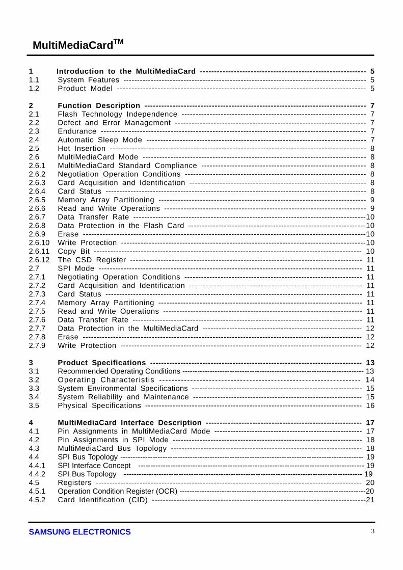
1 Introduction to the MultiMediaCard ----------------------------------------------------------- 5 1.1 System Features ----------------------------------------------------------------------------------------- 5 1.2 Product Model -------------------------------------------------------------------------------------- 5
2 Function Description ------------------------------------------------------------------------------- 7 2.1 Flash Technology Independence ------------------------------------------------------------------ 7 2.2 Defect and Error Management --------------------------------------------------------------------- 7 2.3 Endurance ----------------------------------------------------------------------------------------------- 7 2.4 Automatic Sleep Mode ------------------------------------------------------------------------------- 7 2.5 Hot Insertion -------------------------------------------------------------------------------------------- 8 2.6 MultiMediaCard Mode -------------------------------------------------------------------------------- 8 2.6.1 MultiMediaCard Standard Compliance ----------------------------------------------------------- 8 2.6.2 Negotiation Operation Conditions ----------------------------------------------------------------- 8 2.6.3 Card Acquisition and Identification ---------------------------------------------------------------- 8 2.6.4 Card Status ---------------------------------------------------------------------------------------------- 8 2.6.5 Memory Array Partitioning --------------------------------------------------------------------------- 9 2.6.6 Read and Write Operations ------------------------------------------------------------------------- 9 2.6.7 Data Transfer Rate ------------------------------------------------------------------------------------10 2.6.8 Data Protection in the Flash Card -----------------------------------------------------------------10 2.6.9 Erase -----------------------------------------------------------------------------------------------------10 2.6.10 Write Protection ----------------------------------------------------------------------------------------10 2.6.11 Copy Bit ------------------------------------------------------------------------------------------------- 10 2.6.12 The CSD Register ------------------------------------------------------------------------------------ 11 2.7 SPI Mode ----------------------------------------------------------------------------------------------- 11 2.7.1 Negotiating Operation Conditions ---------------------------------------------------------------- 11 2.7.2 Card Acquisition and Identification --------------------------------------------------------------- 11 2.7.3 Card Status --------------------------------------------------------------------------------------------- 11 2.7.4 Memory Array Partitioning -------------------------------------------------------------------------- 11 2.7.5 Read and Write Operations ------------------------------------------------------------------------- 11 2.7.6 Data Transfer Rate ------------------------------------------------------------------------------------ 11 2.7.7 Data Protection in the MultiMediaCard ----------------------------------------------------------- 12 2.7.8 Erase ----------------------------------------------------------------------------------------------------- 12 2.7.9 Write Protection ---------------------------------------------------------------------------------------- 12
3 Product Specifications ----------------------------------------------------------------------------- 13 3.1 Recommended Operating Conditions ------------------------------------------------------------------------- 13 3.2 Operating Characteristis ----------------------------------------------------------------- 14 3.3 System Environmental Specifications ----------------------------------------------------------------- 15 3.4 System Reliability and Maintenance -------------------------------------------------------------- 15 3.5 Physical Specifications ------------------------------------------------------------------------------- 16
4 MultiMediaCard Interface Description --------------------------------------------------------- 17 4.1 Pin Assignments in MultiMediaCard Mode ------------------------------------------------------- 17 4.2 Pin Assignments in SPI Mode ---------------------------------------------------------------------- 18 4.3 MultiMediaCard Bus Topology ---------------------------------------------------------------------- 18 4.4 SPI Bus Topology -------------------------------------------------------------------------------------------------- 19 4.4.1 SPI Interface Concept ------------------------------------------------------------------------------------------- 19 4.4.2 SPI Bus Topology ------------------------------------------------------------------------------------------------ 19 4.5 Registers ------------------------------------------------------------------------------------------------- 20 4.5.1 Operation Condition Register (OCR) ---------------------------------------------------------------------------20 4.5.2 Card Identification (CID) ------------------------------------------------------------------------------21

SAMSUNG ELECTRONICS 4
MultiMediaCardTM
4.5.3 Relative Card Address (RCA) ----------------------------------------------------------------------- 21 4.5.4 Card Specific Data (CSD) ---------------------------------------------------------------------------- 22 4.6 MultiMediaCard Communication -------------------------------------------------------------------- 30 4.6.1 Commands ----------------------------------------------------------------------------------------------- 30 4.7 Read, Write and Erase Time-out Conditions ----------------------------------------------------- 33 4.8 Card Identification Mode ------------------------------------------------------------------------------ 34 4.8.1 Operating Voltage Range Validation --------------------------------------------------------------- 35 4.9 Data Transfer Mode ------------------------------------------------------------------------------------ 35 4.9.1 Block Read ----------------------------------------------------------------------------------------------- 37 4.9.2 Block Write ----------------------------------------------------------------------------------------------- 37 4.9.3 Erase ------------------------------------------------------------------------------------------------------ 38 4.9.4 Write Protect Management -------------------------------------------------------------------------- 38 4.9.5 Card Lock/Unlock Operation ------------------------------------------------------------------------ 38 4.9.6 Responses ----------------------------------------------------------------------------------------------- 41 4.9.7 Status ------------------------------------------------------------------------------------------------------ 42 4.9.8 Command Response Timing ------------------------------------------------------------------------ 44 4.9.9 Reset ------------------------------------------------------------------------------------------------------ 48 4.10 SPI Communication ----------------------------------------------------------------------------------- 49 4.10.1 Mode Selection ----------------------------------------------------------------------------------------- 49 4.10.2 Bus Transfer Protection ------------------------------------------------------------------------------ 49 4.10.3 Data Read Overview ---------------------------------------------------------------------------------- 50 4.10.4 Data Write Overview ---------------------------------------------------------------------------------- 51 4.10.5 Erase and Write Protect Management ----------------------------------------------------------- 52 4.10.6 Reading CID/CSD Registers ------------------------------------------------------------------------ 53 4.10.7 Reset Sequence --------------------------------------------------------------------------------------- 53 4.10.8 Error Conditions ---------------------------------------------------------------------------------------- 53 4.10.9 Memory Array Partitioning --------------------------------------------------------------------------- 53 4.10.10 Card Lock/Unlock -------------------------------------------------------------------------------------- 53 4.10.11 Commands ----------------------------------------------------------------------------------------------- 54 4.10.12 Responses ----------------------------------------------------------------------------------------------- 56 4.10.13 Data Tokens --------------------------------------------------------------------------------------------- 58 4.10.14 Data Error Token --------------------------------------------------------------------------------------- 59 4.10.15 Clearing Status Bits ------------------------------------------------------------------------------------ 60 4.11 SPI Bus Timing ----------------------------------------------------------------------------------------- 61 4.12 Error Handling ------------------------------------------------------------------------------------------ 64 4.12.1 Error Correction Code (ECC) ----------------------------------------------------------------------- 64 4.12.2 Cyclic Redundancy Check (CRC) ----------------------------------------------------------------- 64
SAMSUNG ELECTRONICS 5
MultiMediaCardTM
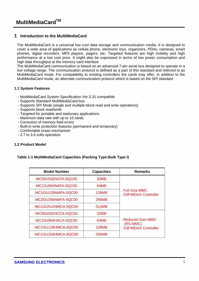
1 Introduction to the MultiMediaCard The MultiMediaCard is a universal low cost data storage and communication media. It is designed to cover a wide area of applications as cellula phone, electronic toys, organizers, PDAs, cameras, smart phones, digital recorders, MP3 players, pagers, etc. Targeted features are high mobility and high performance at a low cost price. It might also be expressed in terms of low power consumption and high data throughput at the memory card interface The MultiMediaCard communication is based on an advanced 7-pin serial bus designed to operate in a low voltage range. The communication protocol is defined as a part of this standard and referred to as MultiMediaCard mode. For compatibility to existing controllers the cards may offer, in addition to the MultiMediaCard mode, an alternate communication protocol which is based on the SPI standard
1.1 System Features
- MultiMediaCard System Specification Ver.3.31 compatible - Supports Standard MultiMediaCard bus - Supports SPI Mode (single and multiple block read and write operations) - Supports block read/write - Targeted for portable and stationary applications - Maximum data rate with up to 10 cards - Correction of memory field errors - Built-in write protection features (permanent and temporary) - Comfortable erase mechanism - 2.7 to 3.6 volts operation
1.2 Product Model
Table 1-1 MultiMediaCard Capacities (Packing Type:Bulk Type I)
Model Number Capacities Remarks
MC56U032NCFA-0QC00 32MB
MC12U064NAFA-0QC00 64MB
MC1GU128NMFA-0QC00 128MB
MC2DU256NMFA-0QC00 256MB
MC1GU512NMCA-0QC00 512MB
. Full Size MMC
. S3F49DAX Controller
MC56U032HCCA-0QC00 32MB
MC12U064HACA-0QC00 64MB
MC1GU128HMCA-0QC00 128MB
MC1GU256HMCA-0QC00 256MB
. Reduced-Size MMC (RS-MMC)
. S3F49DAX Controller

SAMSUNG ELECTRONICS 6
MultiMediaCardTM
Table 1-2 Ordering Information M(1) C(2) X(3) X(4) X(5) X(6) X(7) X(8) X(9) X(10) X(11) X(12) –(13) X(14) X(15) X(16) X(17) X(18)
(1) Module : M (2) Card : C (3) ~(4) : Flash Density 28 : 128Mb 56 : 256Mb 12 : 512Mb 1G : 1Gb 1D : 1Gb DDP 2D : 2Gb DDP (5) Feature U : MultimediaCard (6) ~ (8) Card Density 016 : 16MB 032 : 32MB 064 : 64MB 128 : 128MB 256 : 256MB 512 : 512MB (9) Card Type N : Standard MultiMediaCard H : Reduced-Size MultiMediaCard (10) Flash Generation M : 1st Generation A : 2nd Generation B : 3rd Generation C : 4th Generation D : 5th Generation
(11) Flash Package C : CHIP Y : TSOP 1 V : WSOP F : WSOP(Lead Free) (12) PCB Revision A : None B : 1st Rev. C : 2nd Rev. (13) “ –“ (14) Packing Type 0 : Bulk Type I 1 : Bulk Type II (By White Case) 2 : Bulk Type I (No Label) 3 : Bulk Type II (No Label) 4 : Bulk Type I (Only Back Label) 5 : Bulk Type II (Only Back Label) (15) Controller Q : S3F49DAX (16) Controller Firmware Revision A : None B : 1st Rev. C : 2nd Rev. D : 3rd Rev. E : 4th Rev. (17) ~ (18) Customer Grade “Customer List Reference”
The performance of the communication channel is described in the table below
MultiMediaCard Mode SPI Mode
Three-wire serial data bus (clock, command, data)
Three-wire serial data bus (clock, dataIn, dataOut) + card specific CS signal
Up to 64k cards addressable by the bus protocol
Card selection via a hardware CS signal
Up to 30 cards stackable on a single physical bus
Card stacks require a “per card” CS signal
Easy identification and assignment of session address to individual cards in a card stack
Not available. Card selection via a hardware CS signal
Error-protected data transfer Optional. A non protected data transfer mode is available
single/multiple block read/write command Single/multiple block read/write commands

SAMSUNG ELECTRONICS 7
MultiMediaCardTM
2 Function Description
2.1 Flash Technology Independence The 512 byte sector size of the MultiMediaCard is the same as that in an IDE magnetic disk drive. To write or read a sector (or multiple sectors), the host computer software simply issues a Read or Write command to the MultiMediaCard. This command contains the address and the number of sectors to write/read. The host software then waits for the command to complete. The host software does not get involved in the details of how the flash memory is erased, programmed or read. This is extremely important as flash devices are expected to get more and more complex in the future. Because the MultiMediaCard uses an intelligent on-board controller, the host system software will not require changing as new flash memory evolves. In other words, systems that support the MultiMediaCard today will be able to access future MultiMediaCards built with new flash technology without having to update or change host software.
2.2 Defect and Error Management MultiMediaCards contain a sophisticated defect and error management system. This system is analogous to the systems found in magnetic disk drives and in many cases offers enhancements. For instance, disk drives do not typically perform a read after write to confirm the data is written correctly because of the performance penalty that would be incurred. MultiMediaCards do a read after write under margin conditions to verify that the data is written correctly (except in the case of a Write without Erase Command). In the rare case that a bit is found to be defective, MultiMediaCards replace this bad bit with a spare bit within the sector header. If necessary, MultiMediaCards will even replace the entire sector with a spare sector. This is completely transparent to the host and does not consume any user data space. The MultiMediaCards soft error rate specification is much better than the magnetic disk drive specification. In the extremely rare case a read error does occur, MultiMediaCards have innovative algorithms to recover the data. This is similar to using retries on a disk drive but is much more sophisticated. The last line of defense is to employ powerful ECC to correct the data. If ECC is used to recover data, defective bits are replaced with spare bits to ensure they do not cause any future problems. These defect and error management systems coupled with the solid-state construction give MultiMediaCards unparalleled reliability
2.3 Endurance MultiMediaCards have an endurance specification for each sector of 1,000,000 writes (reading a logical sector is unlimited). This is far beyond what is needed in nearly all applications of MultiMediaCards. Even very heavy use of the MultiMediaCard in cellular phones, personal communicators, pagers and voice recorders will use only a fraction of the total endurance over the typical device’s five year lifetime. For instance, it would take over 100 years to wear out an area on the MultiMediaCard on which a files of any size (from 512 bytes to capacity) was rewritten 3 times per hour, 8 hours a day, 365 days per year.
With typical applications the endurance limit is not of any practical concern to the vast majority of users. 2.4 Automatic Sleep Mode
An important feature of the MultiMediaCard is automatic entrance and exit from sleep mode. Upon completion of an operation, the MultiMediaCard will enter the sleep mode to conserve power if no

SAMSUNG ELECTRONICS 8
MultiMediaCardTM
further commands are received within 5 msec The host does not have to take any action for this to occur. In most systems, the MultiMediaCard is in sleep mode except when the host is accessing it, thus conserving power. When the host is ready to access the MultiMediaCard and it is in sleep mode, any command issued to the MultiMediaCard will cause it to exit sleep and respond. The host does not have to issue a reset first. It may do this if desired, but it is not needed. By not issuing the reset, performance is improved through the reduction of overhead.
2.5 Hot Insertion Support for hot insertion will be required on the host but will be supported through the connector. Connector manufacturers will provide connectors that have power pins long enough to be powered before contact is made with the other pins. Please see connector data sheets for more details. This approach is similar to that used in PCMCIA to allow for hot insertion. This applies to both MultiMediaCard and SPI modes.
2.6 MultiMediaCard Mode
2.6.1 MultiMediaCard Standard Compliance The MultiMediaCard is fully compliant with MultiMediaCard standard specification V3.31. The structure of the Card Specific Data (CSD) register is compliant with CSD structure V1.2.
2.6.2 Negotiating Operation Conditions The MultiMediaCard supports the operation condition verification sequence defined in the MultiMediaCard standard specifications. The MultiMediaCard host should define an operating voltage range that is not supported by the MultiMediaCard. It will put itself in an inactive state and ignore any bus communication. The only way to get the card out of the inactive state is by powering it down and up again. In addition the host can explicitly send the card to the inactive state by using the GO_INACTIVE_STATE command.
2.6.3 Card Acquisition and Identification The MultiMediaCard bus is a single master (MultiMediaCard host) and multi-slaves (cards) bus. The host can query the bus and find out how many cards of which type are currently connected. The MultiMediaCard’s CID register is pre-programmed with a unique card identification number which is used during the acquisition and identification procedure In addition, the MultiMediaCard host can read the card’s CID register using the READ_CID MultiMediaCard command. The CID register is programmed during the MultiMediaCard testing and formatting procedure, on the manufacturing floor. The MultiMediaCard host can only read this register and not write to it.
2.6.4 Card Status MultiMediaCard status is stored in a 32 bit status register which is sent as the data field in the card respond to host commands. Status register provides information about the card’s current state and completion codes for the last host command. The card status can be explicitly read (polled) with the SEND_STATUS command.

SAMSUNG ELECTRONICS 9
MultiMediaCardTM
2.6.5 Memory Array Partitioning Although the MultiMediaCard memory space is byte addressable with addresses ranging from 0 to the last byte, it is not a simple byte array but divided into several structures. Memory bytes are grouped into 512 byte blocks called sectors. Every block can be read, written individually. Erase group is a number of sectors. Its size is the number of consecutive sectors. Any combination of erase groups can be erased in a single erase command. A write command implicitly erases the memory before writing new data into it. Explicit erase command can be used for pre-erasing of memory to speed up the next write operation. Write Protect Groups (WPG) is the minimal units that may have individual write protection. Its size is the number of erase units that will be write protected by on bit. The write/erase access to each WPG can be limited individually. The number of various memory structures, for the different MultiMediaCards are summarized in Table 2-1 Table 2-1 Memory Array Structure
Bytes 32MB 64MB 128MB 256MB 512MB Sectors 62,720 125,440 250,880 501,760 1,003,520 Erase Group
1,960 3,920 980 980 1960
WPG 490 980 245 245 490
Read and Write Operations The MultiMediaCard supports two read/write modes as shown in the above figure. Single Block Mode In this mode the host reads or writes one data block in a pre-specified length block transmission is protected with 16 bit CRC which is generated by the sending unit and checked by the receiving unit. Misalignment is not allowed. Every data block must be contained in a single memory sector. The block length for write operations must be identical to the sector size and the start address aligned to a sector boundary.
Multiple Block Mode This mode is similar to the single block mode, but the host can read/write multiple data blocks (all have the same length) which will be stored or retrieved from contiguous memory addresses starting at the address specified in the command. The operation is terminated with a stop transmission command. Misalignment and block length restrictions apply to multiple blocks as well and are identical to the single block read/write operations. Multiple block read with pre-defined block is supported.
2.6.6 Data Transfer Rate The average data transfer rate for the MultiMediaCard is 1 Mbyte/sec for read and 300 Kbyte/Sec for write (erase time is included) at 3.3 Volts. In block mode, where time gaps can be inserted between data blocks, the maximum clock frequency is 20MHz. The typical access time (latency) for each data block, in read operation, is 1.5ms. The write block operation is done in handshake mode. The card will keep data line DAT low as long as the write operation is in progress and there are no write buffers available
2.6.7 Data Protection in the Flash Card
SAMSUNG ELECTRONICS 10
MultiMediaCardTM
Every sector is protected with an Error Correction Code (ECC). The ECC is generated (in the memory card) when the sectors are written and validated when the data is read. If defects are found, the data is corrected prior to transmission to the host. The MultiMediaCard can be considered error free and no additional data protection is needed. However, if an application uses additional, external, ECC protection, the data organization is defined in the user writeable section of the CSD register
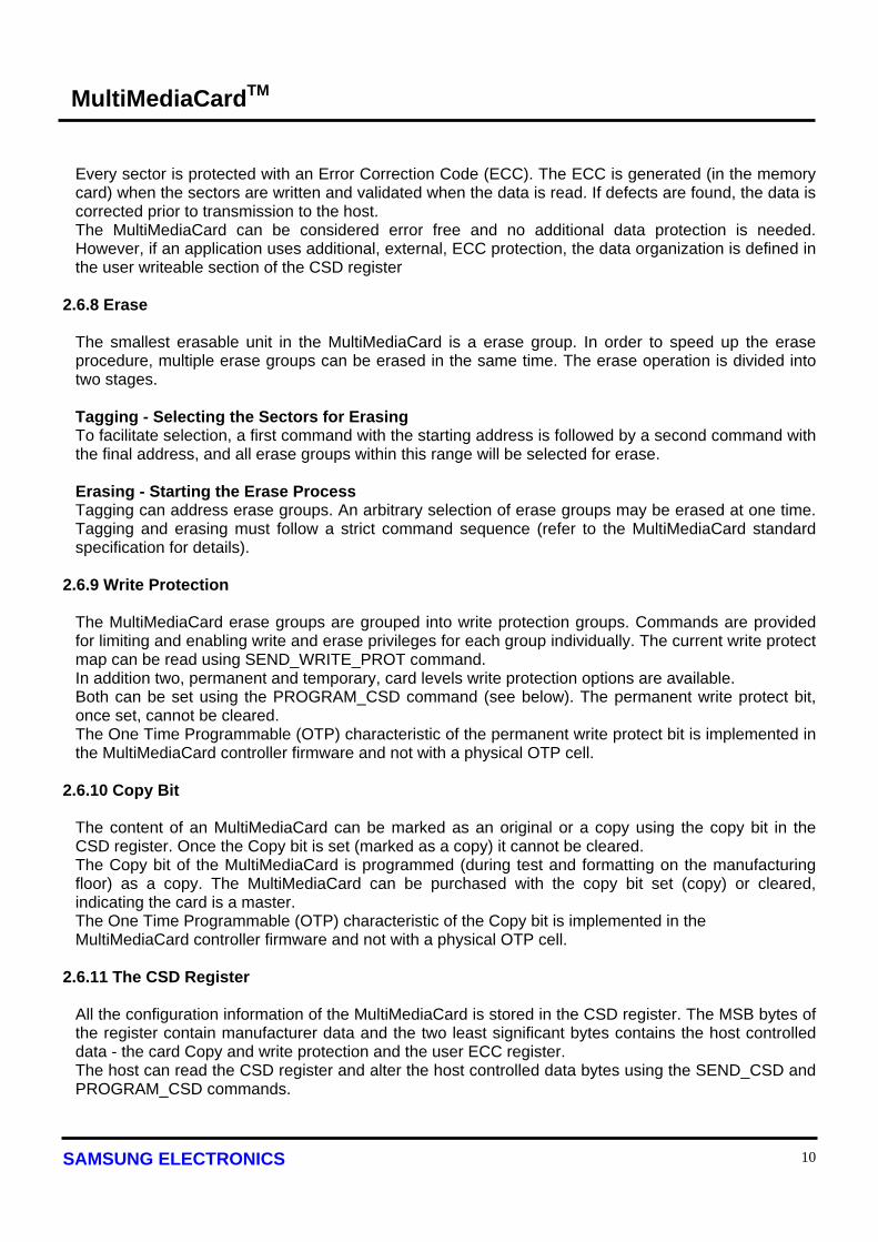
2.6.8 Erase The smallest erasable unit in the MultiMediaCard is a erase group. In order to speed up the erase procedure, multiple erase groups can be erased in the same time. The erase operation is divided into two stages. Tagging - Selecting the Sectors for Erasing To facilitate selection, a first command with the starting address is followed by a second command with the final address, and all erase groups within this range will be selected for erase. Erasing - Starting the Erase Process Tagging can address erase groups. An arbitrary selection of erase groups may be erased at one time. Tagging and erasing must follow a strict command sequence (refer to the MultiMediaCard standard specification for details).
2.6.9 Write Protection The MultiMediaCard erase groups are grouped into write protection groups. Commands are provided for limiting and enabling write and erase privileges for each group individually. The current write protect map can be read using SEND_WRITE_PROT command. In addition two, permanent and temporary, card levels write protection options are available. Both can be set using the PROGRAM_CSD command (see below). The permanent write protect bit, once set, cannot be cleared. The One Time Programmable (OTP) characteristic of the permanent write protect bit is implemented in the MultiMediaCard controller firmware and not with a physical OTP cell.
2.6.10 Copy Bit The content of an MultiMediaCard can be marked as an original or a copy using the copy bit in the CSD register. Once the Copy bit is set (marked as a copy) it cannot be cleared. The Copy bit of the MultiMediaCard is programmed (during test and formatting on the manufacturing floor) as a copy. The MultiMediaCard can be purchased with the copy bit set (copy) or cleared, indicating the card is a master. The One Time Programmable (OTP) characteristic of the Copy bit is implemented in the MultiMediaCard controller firmware and not with a physical OTP cell.
2.6.11 The CSD Register All the configuration information of the MultiMediaCard is stored in the CSD register. The MSB bytes of the register contain manufacturer data and the two least significant bytes contains the host controlled data - the card Copy and write protection and the user ECC register. The host can read the CSD register and alter the host controlled data bytes using the SEND_CSD and PROGRAM_CSD commands.

SAMSUNG ELECTRONICS 11
MultiMediaCardTM
2.7 SPI Mode
The SPI mode is a secondary (optional) communication protocol offered for MultiMediaCard. This mode is a subset of the MultiMediaCard protocol, designed to communicate with an SPI channel, commonly found in Motorola’s (and lately a few other vendors’) microcontrollers.
2.7.1 Negotiating Operation Conditions The operating condition negotiation function of the MultiMediaCard bus is not supported in SPI mode. The host must work within the valid voltage range (2.7 to 3.6 volts) of the card.
2.7.2 Card Acquisition and Identification The card acquisition and identification function of the MultiMediaCard bus is not supported in SPI mode. The host must know the number of cards currently connected on the bus. Specific card selection is done via the CS signal.
2.7.3 Card Status In SPI mode only 16 bits (containing the errors relevant to SPI mode) can be read out of the MultiMediaCard status register.
2.7.4 Memory Array Partitioning Memory partitioning in SPI mode is equivalent to MultiMediaCard mode. All read and write commands are byte addressable.
2.7.5 Read and Write Operations In SPI mode, only single block read/write mode is supported.
2.7.6 Data Transfer Rate In SPI mode only block mode is supported. The typical access time (latency) for each data block, in read operation, is 1.5mS. The write typical access time (latency) for each data block, in read operation, is 1.5mS. The write block operation is done in handshake mode. The card will keep DataOut line low as long as the write operation is in progress and there are no write buffers available.
2.7.7 Data Protection in the MultiMediaCard
Same as for the MultiMediaCard mode.
2.7.8 Erase
Same as in MultiMediaCard mode
2.7.9 Write Protection

SAMSUNG ELECTRONICS 12
MultiMediaCardTM
Same as in MultiMediaCard mode
SAMSUNG ELECTRONICS 13
MultiMediaCardTM
3 Product Specifications
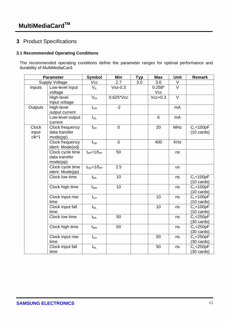
3.1 Recommended Operating Conditions The recommended operating conditions define the parameter ranges for optimal performance and durability of MultiMediaCard.
Parameter Symbol Min Typ Max Unit Remark
Supply Voltage Vcc 2.7 3.0 3.6 V Low-level input voltage
VIL Vss-0.3 0.258* Vcc
V Inputs
High-level Input voltage
VIH 0.625*Vcc Vcc+0.3 V
High-level output current
IOH -2 mA Outputs
Low-level output current
IOL 6 mA
Clock frequency data transfer mode(pp)
fPP 0 20 MHz CL<100pF (10 cards)
Clock frequency ident. Mode(od)
fOD 0 400 KHz
Clock cycle time data transfer mode(pp)
tPP=1/fPP 50 ns
Clock cycle time ident. Mode(pp)
tOD=1/fPP 2.5 us
Clock low time tWL 10 ns CL<100pF (10 cards)
Clock high time tWH 10 ns CL<100pF (10 cards)
Clock input rise time
tLH 10 ns CL<100pF (10 cards)
Clock input fall time
tHL 10 ns CL<100pF (10 cards)
Clock low time tWL 50 ns CL<250pF (30 cards)
Clock high time tWH 50 ns CL<250pF (30 cards)
Clock input rise time
tLH 50 ns CL<250pF (30 cards)
Clock input clk*1
Clock input fall time
tHL 50 ns CL<250pF (30 cards)

SAMSUNG ELECTRONICS 14
MultiMediaCardTM
3.2 Operating Characteristics The operating characteristics are parameters measured in a MultiMediaCard system assuming the recommended operating conditions.
Parameter Symbol Min Typ Max Unit Remark
32MB 65 mA 64MB 65 mA 128MB 65 mA 256MB 65 mA
High speed supply current
512MB 65 mA
At 20MHz, 3.6V
32MB 100 uA 64MB 100 uA 128MB 100 uA 256MB 100 uA
Minimal supply current
512MB 100 uA
At 0Hz, 3.6V Standby
State
All digital inputs
(including I/O
current)
Input leakage current
-10 10 uA
High-level output voltage
VOH 0.75*Vcc V At min IOH All outputs
Low-level output voltage
VOL 0.125Vcc V At max IOL
Input set-up time
tISU 3 ns Inputs: CMD,DAT(Referred to SCLK),
CS
Input hold time tIH 3 ns
Output set-up time
tOSU 5 ns Outputs: CMD,DAT(Referred to CLK),
D0 (Referred to SCLK)
Output hold time
tOH 5 ns At tLH=10ns

SAMSUNG ELECTRONICS 15
MultiMediaCardTM
Figure 3-1 Timing Diagram of Data Input and Output 3.3 System Environmental Specifications
Temperature Operating Non-Operating
-25’C to 85’C -40’C to 85’C
Humidity Non-Operating 8% to 95%. Non-condensing
Acoustic Noise 0 dB
Vibration Operating Non-Operating
5 G Peak to Peak max. 5 G Peak to Peak max.
Shock Operating Non-Operating
1,000 G max 1,000 G max
3.4 System Reliability and Maintenance
MTBF >1,000,000 hours Preventive Maintenance None Data Reliability < 1 non-recoverable error in 1014 bits read Endurance 1,000,000 write/erase cycles

SAMSUNG ELECTRONICS 16
MultiMediaCardTM
3.5 Physical Specifications Dimensions of Normal MMC(24mm x 32mm x 1.4mm)
Dimensions of RS-MMC(24mm x 18mm x 1.4mm)

SAMSUNG ELECTRONICS 17
MultiMediaCardTM
4 MultiMediaCard Interface Description
4.1 Pin Assignments in MultiMediaCard Mode
Table 4-1 MultiMediaCard Pad Definition
Pin No. Name Type*1 Description 1 RSV NC No connection 2 CMD I/O/PP/OD Command/Response 3 Vss1 S Ground 4 Vcc S Power supply 5 CLK I Clock 6 Vss2 S Ground 7 DAT I/O/PP Data
Note : 1. S: power supply; I: input; O: output; PP: push-pull; OD: open-drain; NC: No connection or VIH
Figure 4-1 MultiMediaCard Mode I/O drivers

SAMSUNG ELECTRONICS 18
MultiMediaCardTM
4.2 Pin Assignments in SPI Mode
Table 4- 2 SPI Pad Definition
Pin No. Name Type*1 Description 1 CS I Chip Select 2 DI I Data In 3 Vss S Ground 4 Vcc S Power supply 5 SCLK I Clock 6 Vss2 S Ground 7 DO O/PP Data out
Note : 1. S: power supply; I: input; O: output; PP: push-pull; OD: open-drain; NC: No connection or VIH
4.3 MultiMediaCard Bus Topology
The MultiMediaCard bus has three communication lines and four supply lines:
- CMD: Command is a bi-directional signal. Host and card drivers are operating in two modes, open
drain and push pull. - DAT: Data is a bi-directional signal. Host and card drivers are operating in push pull mode. - CLK: Clock is a host to card signal. CLK operates in push pull mode. - VDD: VDD is the power supply line for all cards. - VSS[1:2]: VSS are two ground lines.
Figure 4-2 Bus Circuitry Diagram
The ROD is switched on and off by the host synchronously to the open-drain and push-pull mode transitions. RDAT and RCMD are pull-up resistors protecting the CMD and the DAT line against bus floating when no card is inserted or when all card drivers are in a hi-impedance mode. A constant current source can replace the ROD by achieving a better performance (constant slopes for the signal

SAMSUNG ELECTRONICS 19
MultiMediaCardTM
rising and falling edges). If the host does not allow the switchable ROD implementation, a fix RCMD can be used. Consequently the maximum operating implementation, a fix RCMD can be used. Consequently the maximum operating frequency in the open drain mode has to be reduced in this case.
4.4 SPI Bus Topology 4.4.1 SPI Interface Concept The Serial Peripheral Interface (SPI) is a general-purpose synchronous serial interface originally found on certain Motorola micro-controllers. The MultiMediaCard SPI interface is compatible with SPI hosts available on the market. As any other SPI device the MultiMediaCard SPI channel consists of the following 4 signals:
- CS : Host to card chip select signal - CLK : Host to card clock signal - DataIn : Host to card data signal - DataOut : Card to host data signal
Another SPI common characteristic, which is implemented in the MultiMediaCard card as well, is byte transfers. All data tokens are multiples of 8 bit bytes and always byte aligned to the CS signal. The SPI standard defines the physical link only and not the complete data transfer protocol. The MultiMediaCard uses a subset of the MultiMediaCard protocol and command set. 4.4.2 SPI Bus Topology The MultiMediaCard card identification and addressing algorithms are replaced by hardware Chip Select (CS) signal. There are no broadcast commands. A card (slave) is selected, for every command, by asserting (active low) the CS signal (see Figure 4-3). The CS signal bust is continuously active for the duration of the SPI transaction (command, response and data). The only exception is card-programming time. At this time the host can de-assert the CS signal without affecting the programming process. The bi-directional CMD and DAT lines are replaced by unidirectional dataIn and dataOut signals. This eliminates the ability of executing commands while data is being read or written and, therefore, eliminates the sequential and multi block read/write operations. The SPI channel supports only single block read/write.
Figure 4-3 SPI Bus System

SAMSUNG ELECTRONICS 20
MultiMediaCardTM
4.5 Registers
Table 4-3 MultiMediaCard Information Registers
Name Width Type Description OCR 32 Programmed by the
manufacturer. Read only for user
Supported voltage range, card power up status bit
CID 128 Programmed by the manufacturer. Read only for user
Card identification number, card individual number for identification.
RCA 16 Programmed during initialization, not readable
Relative card address, local system address of a card, dynamically assigned by the host during initialization.
CSD 128 Programmed by the manufacturer. Partially Programmable by the user
Card specific data, information about the card operation conditions.
CID and RCA are used for identifying and addressing MultiMediaCard. CSD contains the card specific data record. This record is a set of information fields to define the operation conditions of the MultiMediaCard. For the user the CID and the OCR are read only registers. They are read out by special commands (refer to Chapter “Commands”). The RCA registers are write only registers. Unlike CID and CSD, RCA looses its contents after powering down the card. Its value is reassigned in each initialization cycle. The MultiMediaCard registers usage in SPI mode is summarized in Table “MultiMediaCard Registers in SPI Mode Table 4-4 Information Registers in SPI Mode
Name Width (bytes) Available Description OCR 4 Yes Operation condition register CID 16 Yes Card identification data (serial number,
manufacturer ID etc.) RCA No CSD 16 Yes Card specific data, information about the card
operation conditions 4.5.1 Operation Condition Register (OCR)
This register indicates supported voltage range of MultiMediaCards. It is a 32 bit wide register and for read only.
Table 4-5 OCR Fields

SAMSUNG ELECTRONICS 21
MultiMediaCardTM
OCR Slice Field Value Note D31 Card power up status bit (busy) 0 or 1 D[30-24] Reserved 0 D23 3.5 ~ 3.6V 1 D22 3.4 ~ 3.5V 1 D21 3.3 ~ 3.4V 1 D20 3.2 ~ 3.3V 1 D19 3.1 ~ 3.2V 1 D18 3.0 ~ 3.1V 1 D17 2.9 ~ 3.0V 1 D16 2.8 ~ 2.9V 1 D15 2.7 ~ 2.8V 1 D14 2.6 ~ 2.7V 0 D13 2.5 ~ 2.6V 0 D12 2.4 ~ 2.5V 0 D11 2.3 ~ 2.4V 0 D10 2.2 ~2.3V 0 D9 2.1 ~ 2.2V 0 D8 2.0 ~ 2.1V 0 D7 1.65 ~ 1.95V 0 D[6-0] Reserved 0
4.5.2 Card Identification (CID)
This register contains the card identification information used during the card identification procedure. It is a 128 bit wide register, one-time programmable by the provider. The CID is divided into eight slices:
Table 4-6 CID Fields
Name Field Width CID-Slice Manufacturer ID*1 MID 8 [127:120] OEM/Application ID OID 16 [119:104] Product name PNM 48 [103:56] Product revision PRV 8 [55:48] Product serial number PSN 32 [47:16] Manufacturing date MDT 8 [15:8] CRC checksum CRC 7 [7:1] not used, always 1 -- 1 [0:0]
Note: 1. The value of MID is 0x15.

SAMSUNG ELECTRONICS 22
MultiMediaCardTM
4.5.3 Relative Card Address (RCA)
The 16-bit relative card address register carries the card address assigned by the host during the card identification. This address is used for the addressed host to card communication after the card identification procedure. The default value of the RCA register is 0x0001. The value 0x0000 is reserved to set all cards in Standby State with the command SELECT_DESELECT_CARD (CMD7). The RCA is programmed with the command SET_RELATIVE_ADDRESS (CMD3) during the initialization procedure. The content of this register is lost after power down. The default value is assigned when an internal reset is applied by the power up detection unit of the MultiMediaCard.
4.5.4 Card Specific Data (CSD)
The card specific data register describes how to access the card content. The CSD defines card operating parameters like maximum data access time, data transfer speed. Table 4-7 CSD Field
Name Field Width CSD-slice Value Type
CSD structure CSD_STRUCTURE 2 [127:126] 0x2 read only Spec version SPEC_VERS 4 [125:122] 0x3 read only Reserved -- 2 [121:120] 0x0 read only Data read access-time-1
TAAC 8 [119:112] 0×26 (1.5 ms)
read only
Data read access-time-2 in CLK cycles NAC*100)
NSAC 8 [111:104] 0×01 (100 cycles)
read only
Max. data transfer rate
TRAN_SPEED 8 [103:96] 0×2A (20MHz,Max)
read only
Card command classes
CCC 12 [95:84] 0×0F5 (Class 0,2,4,5, 6, 7)
read only
Max. read data block length
READ_BL_LEN 4 [83:80] 0×9(512 bytes) read only
Partial blocks for read allowed
READ_BL_PARTIAL 1 [79:79] 0x0(Disabled) read only
Write block misalignment
WRITE_BLK_MISALIGN 1 [78:78] 0x0(Disabled) read only
Read block misalignment
READ_BLK_MISALIGN 1 [77:77] 0x0 (Disabled) read only
DSR implemented DSR_IMP 1 [76:76] 0x0 (Disabled) read only Reserved -- 2 [75:74] 0x0 read only Device size C_SIZE 12 [73:62] *1 read only
Max. read current at VDD min
VDD_R_CURR_MIN 3 [61:59] *2 read only
Max. read current at VDD max
VDD_R_CURR_MAX 3 [58:56] *2 read only
Max. write current at VDD min
VDD_W_CURR_MIN 3 [55:53] *2 read only
Max. write current at VDD max
VDD_W_CURR_MAX 3 [52:50] *2 read only

SAMSUNG ELECTRONICS 23
MultiMediaCardTM
Device size multiplier
C_SIZE_MULT 3 [49:47] *3 read only
Erase group size ERASE_GRP_SIZE 5 [46:42] *5 read only Erase group size multiplier
ERASE_GRP_MULT 5 [41:37] 0x1F read only
Write protect group size
WP_GRP_SIZE 5 [36:32] 0x3 read only
Write protect group enable
WP_GRP_ENABLE 1 [31:31] 0x1 read only
Manufacturer default ECC
DEFAULT_ECC 2 [30:29] 0x0 read only
Write speed factor R2W_FACTOR 3 [28:26] 0x4 read only Max. write data block length
WRITE_BLK_LEN 4 [25:22] 0x9 read only
Partial blocks for write allowed
WRITE_BLK_PARTIAL 1 [21:21] 0x0 read only
Reserved -- 5 [20:16] 0x0 read only File format group FILE_FORMAT_GRP 1 [15:15] 0x0 Read/Write Copy flag(OTP) COPY 1 [14:14] 0x1 Read/Write Permanent write protection
PERM_WRITE_PROTECT
1 [13:13] 0x0 Read/Write
Temporary write protection
TMP_WRITE_PROTECT 1 [12:12] 0x0 Read/Write/ erase
File format FILE_FORMAT 2 [11:10] 0x0 Read/Write ECC code ECC 2 [9:8] 0x0 Read/Write/
erase CRC CRC 7 [7:1] × Read/Write/
erase Not used, always 1 0 [0:0] 0x1 read only
Notes: 1. This field is depended on the model. Refer to also C_SIZE_MULT 2. This field is depended on the model 3. This field is depended on the model. Refer to also C_SIZE 4. x means user programmable 5. This field is depended on the model. Refer to also ERASE_GRP_SIZE
Some of the CSD fields are one-time or multiple programmable by the customer or provider. All other field values are fixed. The following section describes the CSD fields and their values for MultiMediaCards :
CSD Register Structure
CSD_STRUCTURE CSD Register Structure “10” CSD version No. 1.2
The CSD version of these MultiMediaCards is related to the “MultiMediaCard system specification, Version 3.31”. The parameter CSD_STRUCTURE has permanently the value “10”.

SAMSUNG ELECTRONICS 24
MultiMediaCardTM
SPEC_VERS Defines the Spec version supported by the card. It includes the commands set definition and the definition of the card responses. The card identification procedure is compatible for all spec versions.
SPEC_VERS System specification version number “0011” System specification version 3.31
The Spec version of these Samsung MultiMediaCards is related to the “MultiMediaCard system specification,Version 3.31”. The parameter SPEC_VERS has permanently the value “0011”. TAAC Defines the asynchronous data access time:
TAAC bit Description Values 2:0 Time exponent 0 = 1 ns, 1 = 10 ns, 2 = 100 ns, 3 = 1
ms, 4 = 10 ms, 5= 100 ms, 6 = 1 ms, 7 = 10 ms
6:3 Time mantissa 0 = reserved, 1 = 1.0, 2 = 1.2, 3 = 1.3, 5 = 1.5, 5 = 2.0, 6 = 2.5, 7 = 3.0, 8 = 3.5, 9 = 4.0, A = 4.5,B = 5.0, C = 5.5, D = 6.0, E = 7.0, F = 8.0
7 Reserved Always ‘0’ The value for the asynchronous delay for these MultiMediaCards is 1.5 ms. The coded TAAC value is 0x26 (= 1.5 ms). NSAC Defines the worst case for synchronous data access time. The unit for NSAC is 100-clock cycles. Therefore, maximum value for the data access time is 25.6K clock cycles. The total access time NAC as expressed in the Table “Timing Values” is the sum of both TAAC and NSAC. It has to be computed by the host for actual clock rate. The read access time should be interpreted as a typical delay for the first data bit of a data block or stream. The value of NSAC for these MultiMediaCards is 0x01 (100-clock cycles). For more details refer to Chapter “Operating Characteristics”. TRAN_SPEED The following table defines the maximum data transfer rate TRAN_SPEED: Maximum Data Transfer Rate Definition
TRAN_SPEED bit Description Values 2:0 Transfer rate exponent 0 = 100 kbit/s, 1 = 1 Mbit/s, 2 = 10
Mbit/s, 3 = 100 Mbit/s, 4...7 = reserved
6:3 Time mantissa 0x0 = reserved, 0x1 = 1.0, 0x2 = 1.2, 0x3 = 1.3, 0x4 = 1.5, 0x5 = 2.0, 0x6 = 2.5, 0x7 = 3.0, 0x8 = 3.5, 0x9 = 4.0, 0xA = 4.5, 0xB = 5.0, 0xC = 5.5, 0xD

SAMSUNG ELECTRONICS 25
MultiMediaCardTM
= 6.0, 0xE = 7.0, 0xF = 8.0 7 Reserved Always ‘0’
These MultiMediaCards support a transfer rate between 0 and 20Mb/s. The parameter TRAN_SPEED is 0x2A. CCCThe MultiMediaCard command set is divided into subsets (command classes). The card command class register CCC defines which command classes are supported by this card. A set CCC bit means that the corresponding command class is supported. For command class definition refer to Table “ Command Classes”. Supported Card Command Classes
CCC bit Supported card command classes 0 Class 0 1 Class 1 ….. ….. 11 Class 11
These MultiMediaCards support the command classes 0,2,4,5,6 and 7. The parameter CCC is permanently assigned to the value 0x0F5. READ_BLK_LEN The data block length is computed as 2^READ_BLK_LEN. Data Block Length
READ_BLK_LEN Block length 0 20 = 1 byte 1 21 = 2 bytes ….. ….. 11 211 = 2,048 bytes 12-15 Reserved
The value of the parameter READ_BLK_LEN is 0x09 (512 bytes). READ_BLK_PARTIAL READ_BLK_PARTIAL defines whether partial block sizes can be used in block read command. READ_BLK_PARTIAL = 0 means that only the block size defined by READ_BLOCK_LEN can be used for block-orinted data transfer. READ_BLK_PARTIAL = 1 means that smaller blocks can be used as well. The minimum block size will be equal to minimum addressable unit (one byte). WRITE_BLK_MISALIGN Defines if the data block to be written by one command can be spread over more than one physical blocks of the memory device. The size of the memory block is defined in WRITE_BLK_LEN.

SAMSUNG ELECTRONICS 26
MultiMediaCardTM
WRITE_BLK_MISALIGN is permanently assigned to the value “0”, signaling that crossing physical block boundaries is not allowed. READ_BLK_MISALIGN Defines if the data block to be read by one command can be spread over more than one physical block of the memory device. The size of the data block is defined in READ_BLK_LEN. READ_BLK_MISALIGN = 0 signals that crossing physical block boundaries is not allowed. READ_BLOCK_MISALIGN = 1 signals that crossing physical block boundaries is allowed. These MultiMediaCards do not support read block operations with boundary crossing. The parameter READ_BLK_MISALIGN is permanently assigned to the value “0”. DSR_IMP Defines if the configurable driver stage option is integrated on the card or not. If implemented a driver stage register (DSR) must be implemented also.
DSR_IMP DSR type 0 No DSR implemented 1 DSR implemented
The parameter DSR_IMP is permanently assigned to the value “0”. C_SIZE This parameter is used to compute the card capacity. The card capacity is computed from the entries C_SIZE, C_SIZE_MULT and READ_BLK_LEN as follows:
Memory Capacity = BLOCKNR*BLOCK_LEN
Where BLOCKNR = (C_SIZE+1)*MULT MULT = 2C_SIZE_MULT+2 (C_SIZE_MULT < 8) BLOCK_LEN = 2READ_BLK_LEN, (READ_BLK_LEN < 12)
The following table shows the card capacity for each model.
C-SIZE C_SIZE_MULT READ_BLK_LEN Card Capacity 0x7A7 3 9 32Mbytes 0xF4F 3 9 64Mbytes 0x3D3 6 9 128Mbytes 0x3D3 7 9 256Mbytes 0x7A7 7 9 512Mbytes
VDD_R_CURR_MIN, VDD_W_CURR_MIN The maximum supply current at the minimum supply voltage VCC (2.7 V) is coded as follows :

SAMSUNG ELECTRONICS 27
MultiMediaCardTM
Maximum Supply Current Consumption at VCC = 2.7 V
VDD_R_CURR_MIN / VDD_W_CURR_MIN Code for current consumption at 2.7 V 2:0 2:0 0 = 0.5 mA; 1 = 1 mA; 2 = 5 mA;
3 = 10 mA; 4 = 25 mA; 5 = 35 mA; 6 = 60 mA; 7 = 100 mA
VDD_R_CURR_MAX, VDD_W_CURR_MAX The maximum supply current at the maximum supply voltage VCC (3.6 V) is coded as follows: Maximum Supply Current Consumption at VCC = 3.6 V
VDD_R_CURR_MAX / VDD_W_CURR_MAX Code for current consumption at 3.6 V 2:0 0 = 1 mA; 1 = 5 mA; 2 = 10 mA; 3 = 25 mA;
4 = 35 mA; 5 = 45 mA; 6 = 80mA; 7 = 200 mA C_SIZE_MULT This parameter is used for coding a factor MULT for computing the total device size (refer to ‘C_SIZE) The factor MULT is defined as 2C_SIZE_MULT+2. ERASE_GRP_SIZE The contents of this register are a 5bit binary coded value, used to calculate the size of the erasable unit of these MultimediaCard. The size of the erase unit (also referred to as erase group in chapter “memory Array Partitioning”) is determined by the ERASE_GRP_SIZE and the ERASE_GRP_MULT entries of the CSD
Size of erasable unit = (ERASE_GRP_SIZE + 1) * (ERASE_GRP_MULT + 1) The following table shows the size of erase group for each model.
ERASE_GRP_SIZE ERASE_GRP_MULT Card Capacity 0x0 0x1F 32Mbytes 0x0 0x1F 64Mbytes 0x7 0x1F 128Mbytes 0xF 0x1F 256Mbytes 0xF 0x1F 512Mbyes
ERASE_GRP_MULT A 5bit binary coded value is used for calculating the size of the erasable unit of these MultiMediaCards. The parameter ERASE_GRP_MULT is permanently assigned to the value 0x1F. See ERASE_GRP_SIZE section for detailed description. WP_GRP_SIZE The size of a write protection group. The content of this register is a binary coded value defining the number of erase group. This parameter's value is 8, which means that a write protect group size is 128

SAMSUNG ELECTRONICS 28
MultiMediaCardTM
kByte. WP_GRP_ENABLE The value is set to ‘1’, meaning group write protection is enabled. DEFAULT_ECC Set by the card manufacturer and defines the ECC code, which is recommended to use (e.g. the device is tested for). The value is set to ‘0’, indicating that no designated ECC is recommended. R2W_FACTOR Defines the typical block program time as a multiple of the read access time. The following table defines the field format.
R2W_FACTOR Multiples of read access time 0 1 1 2 (Write half as fast as read) 2 4 3 8 4 16 5 32 6 64 7 128
This parameter value is 4 for these MultiMediaCards. WRITE_BLK_LEN Block length for write operation. See READ_BL_LEN for field coding. WRITE_BLK_PARTIAL WRITE_BLK_PARTIAL defines whether partial block sizes can be used in block wrtie commands. WRITE_BLK_PARTIAL = 0 means that only the block size defined by WRITE_BLOCK_LEN can be used for block-orinted data transfer. WRITE_BLK_PARTIAL = 1 means that smaller blocks can be used as well. The minimum block size will be equal to minimum addressable unit (one byte). These MultiMediaCards support partial block read. The parameter WRITE_BLK_PARTIAL is permanently assigned to the value “0”. FILE_FORMAT_GRP Indicated the selected group of file formats. This fiels is read-only for ROM. The usage of this fiels is shown in table “File_Formats” COPY Defines if the contents are an original (= 0) or a copy (= 1). The COPY bit is a one time programmable bit, being set by the customer.

SAMSUNG ELECTRONICS 29
MultiMediaCardTM
PERM_WRITE_PROTECT Permanently protects the whole card content against overwriting or erasing (all write and erase commands for this card is a permanently disabled). This parameter is one-time programmable by the customer. The default value is ‘0’ (not protected). TMP_WRITE_PROTECT Temporarily protects the whole card content from being overwritten or erased (all write and erase commands for this card are temporarily disabled). This parameter is programmable by the customer. The default value is ‘0’ (not protected). FILE_FORMAT Indicates the file format on the card. This field is read-only for ROM. The following formats are defined.
FILE_FORMAT_GRP
FILE_FORMAT
Type
0 0 Hard disk-like file system with partition table 0 1 DOS FAT (floppy-like) with boot sector only (no partition table)0 2 Universal File Format 0 3 Others/Unknown 1 0,1,2,3 Reserved
ECC Defines the ECC code that was used for storing data on the card. This field is used by the host (or application) to decode the user data. The following table defines the field format.
ECC ECC Type Maximum number of correctable bits 0 None (default) None 1 BCH (542,512) 3 2-3 0,1,2,3 -
The content provider or customer defines which kind of error correction may be used to protect the contents of MultiMediaCard. This value is programmable. CRC7 The CRC7 contains the check sum for the CSD content. The check sum is computed according to chapter “Cyclic Redundancy Check(CRC)”.

SAMSUNG ELECTRONICS 30
MultiMediaCardTM
4.6 MultiMediaCard Communication
All communication between host and cards is controlled by the host (master). The host sends commands and, depending on the command, receives a corresponding response from the selected card. In this chapter the commands to control the MultiMediaCard, the card responses and the contents of the status and error field included in the responses, are defined.
4.6.1 Commands
The command set of the MultiMediaCard system is divided into classes corresponding to the type of card. The MultiMediaCard supports the following command classes: Table 4-8 Command Classes

SAMSUNG ELECTRONICS 31
MultiMediaCardTM
Class Command Class Description 0 1 2 3 4 7 9 10 12 13
Class 0
15
Basic
Calss 1 11 Stream read (not supported) 16 17 Class 2 18
Block read
Class 3 20 Stream write (not supported) 24 25 26 Class 4
27
Block write
32 33 34 35 36 37
Class 5
38
Erase (not supported CMD 32~34 and 37 according to MMC system spec 3.31)
28 29 Class 6 30
Write protection
Class 7 42 Lock card
Class 0 is mandatory and supported by all cards. It represents the card identification and initialization commands, which are intended to handle different cards and card types on the same bus lines. The Card Command Class (CCC) is coded in the card specific data register of each card, so that the host knows how to access the card. There are four kinds of commands defined on the MultiMediaCard bus: - broadcast commands (bc) sent on CMD line, no response. - broadcast commands with response (bcr) sent on CMD line, response (all cards simultaneously) on CMD line - addressed (point-to-point) commands (ac) sent on CMD line, response on CMD line. - addressed (point-to-point) data transfer commands (adtc) sent on CMD line, response on CMD line, data transfer on DAT line. The command transmission always starts with the MSB. Each command starts with a start bit and ends with a CRC command protection field followed by an end bit. The length of each command frame is fixed to 48 bits (2.4 us at 20 MHz):
SAMSUNG ELECTRONICS 32
MultiMediaCardTM
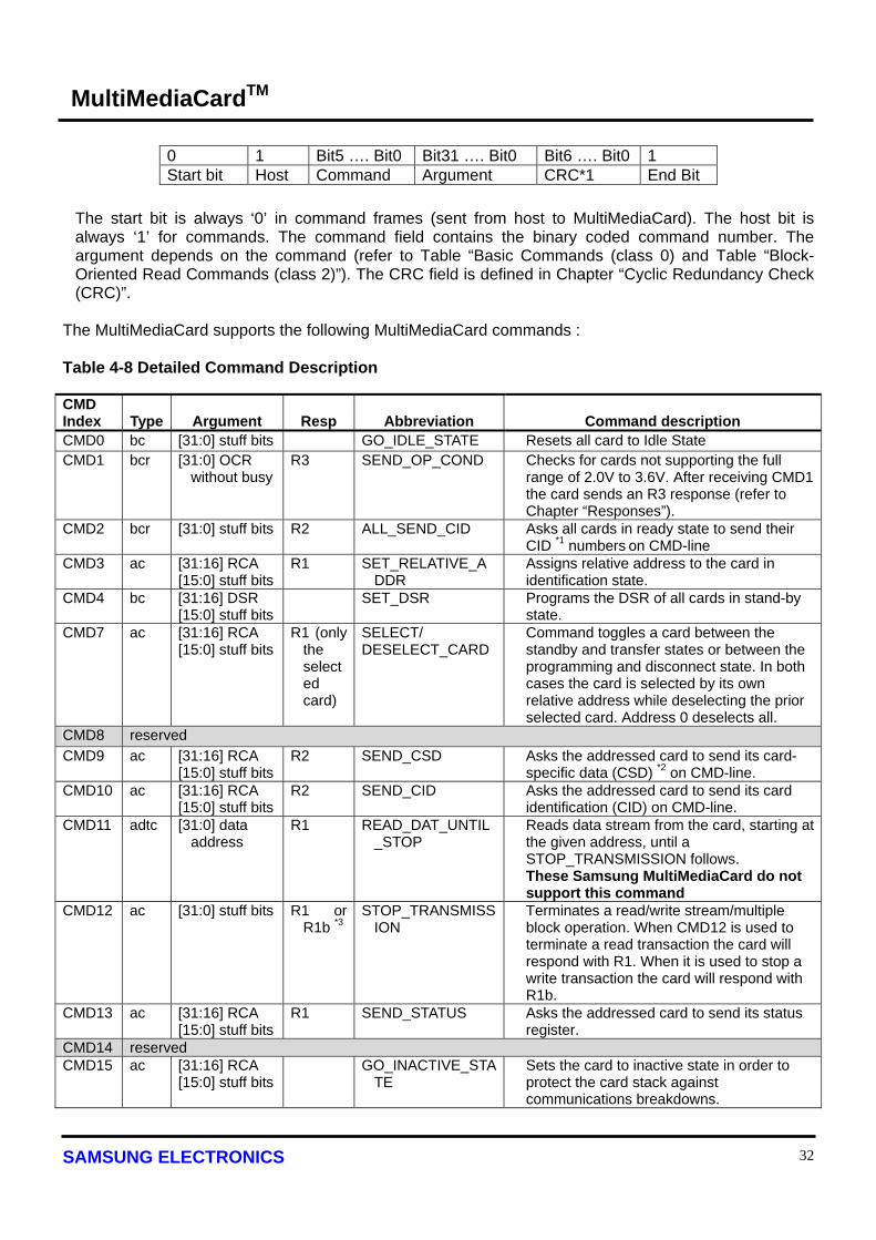
0 1 Bit5 …. Bit0 Bit31 …. Bit0 Bit6 …. Bit0 1 Start bit Host Command Argument CRC*1 End Bit
The start bit is always ‘0’ in command frames (sent from host to MultiMediaCard). The host bit is always ‘1’ for commands. The command field contains the binary coded command number. The argument depends on the command (refer to Table “Basic Commands (class 0) and Table “Block-Oriented Read Commands (class 2)”). The CRC field is defined in Chapter “Cyclic Redundancy Check (CRC)”.
The MultiMediaCard supports the following MultiMediaCard commands :
Table 4-8 Detailed Command Description
CMD Index Type Argument Resp Abbreviation Command description CMD0 bc [31:0] stuff bits ㅡ GO_IDLE_STATE Resets all card to Idle State CMD1 bcr [31:0] OCR
without busy R3 SEND_OP_COND Checks for cards not supporting the full
range of 2.0V to 3.6V. After receiving CMD1 the card sends an R3 response (refer to Chapter “Responses”).
CMD2 bcr [31:0] stuff bits R2 ALL_SEND_CID Asks all cards in ready state to send their CID *1 numbers on CMD-line
CMD3 ac [31:16] RCA [15:0] stuff bits
R1 SET_RELATIVE_ADDR
Assigns relative address to the card in identification state.
CMD4 bc [31:16] DSR [15:0] stuff bits
ㅡ SET_DSR Programs the DSR of all cards in stand-by state.
CMD7 ac [31:16] RCA [15:0] stuff bits
R1 (only the selected card)
SELECT/ DESELECT_CARD
Command toggles a card between the standby and transfer states or between the programming and disconnect state. In both cases the card is selected by its own relative address while deselecting the prior selected card. Address 0 deselects all.
CMD8 reserved CMD9 ac [31:16] RCA
[15:0] stuff bits R2 SEND_CSD Asks the addressed card to send its card-
specific data (CSD) *2 on CMD-line. CMD10 ac [31:16] RCA
[15:0] stuff bits R2 SEND_CID Asks the addressed card to send its card
identification (CID) on CMD-line. CMD11 adtc [31:0] data
address R1 READ_DAT_UNTIL
_STOP Reads data stream from the card, starting at the given address, until a STOP_TRANSMISSION follows. These Samsung MultiMediaCard do not support this command
CMD12 ac [31:0] stuff bits R1 or R1b *3
STOP_TRANSMISSION
Terminates a read/write stream/multiple block operation. When CMD12 is used to terminate a read transaction the card will respond with R1. When it is used to stop a write transaction the card will respond with R1b.
CMD13 ac [31:16] RCA [15:0] stuff bits
R1 SEND_STATUS Asks the addressed card to send its status register.
CMD14 reserved CMD15 ac [31:16] RCA
[15:0] stuff bits ㅡ GO_INACTIVE_STA
TE Sets the card to inactive state in order to protect the card stack against communications breakdowns.

SAMSUNG ELECTRONICS 33
MultiMediaCardTM
CMD16 ac [31:0] block length
R1 SET_BLOCKLEN Selects a block length (in bytes) for all following block commands (read and write). *4
CMD17 adtc [31:0] data address
R1 READ_SINGLE_BLOCK
Reads a block of the size selected by the SET_BLOCKLEN command. *5
CMD18 adtc [31:0] data address
R1 READ_MULTIPLE_BLOCK
Continuously send blocks of data until interrupted by a stop.
CMD19 reserved CMD20 adtc [31:0] data
address R1 WRITE_DAT_UNTIL
_STOP Writes data stream from the host, starting at the given address, until a STOP_TRANSMISSION follows. These Samsung MultiMediaCard do not support this command
CMD21 … CMD22
reserved
CMD23 ac [31:16] set to 0 [15:0] number
of blocks
R1 SET_BLOCK_COUNT
Defines the number of blocks which are going to be transferred in the immediatedly succeeding multiple block read or write command.
CMD24 adtc [31:0] data address
R1 WRITE_BLOCK Writes a block of the size selected by the SET_BLOCKLEN command. *6
CMD25 adtc [31:0] data address
R1 WRITE_MULTIPLE_BLOCK
Continuously writes blocks of data until a STOP_TRANSMISSION follows.
CMD26 adtc [31:0] stuff bits R1 PROGRAM_CID Programming of the card identification register. This command is only done once per MultiMediaCard card. The card has some hardware to prevent this operation after the first programming. Normally this command is reserved for the manufacturer.
CMD27 adtc [31:0] stuff bits R1 PROGRAM_CSD Programming of the programmable bits of the CSD.
CMD28 ac [31:0] data address
R1b SET_WRITE_PROT If the card has write protection features, this command sets the write protection bit of the addressed group. The properties of write protection are coded in the card specific data (WP_GRP_SIZE).
CMD29 ac [31:0] data address
R1b CLR_WRITE_PROT If the card provides write protection features, this command clears the write protection bit of the addressed group.
CMD30 adtc [31:0] write protect data address
R1(7) SEND_WRITE_PROT
If the card provides write protection features, this command asks the card to send the status of the write protection bits. *7
CMD31 Reversed
CMD35 ac [31:0] data address
R1 TAG_ERASE_GROUP_START
Sets the address of the first erase group within a range to be selected for erase
CMD36 ac [31:0] data address
R1 TAG_ERASE_GROUP_END
Sets the address of the last erase group within a continuous range to be selected for erase.
CMD38 ac [31:0] stuff bits R1b ERASE Erases all previously selected sectors CMD42 adtc [31:0] stuff bits R1b LOCK_UNLOCK Used to set/reset the password or
lock/unlock the card. The size of the data block is set by the SET_BLOCK_LEN command.

SAMSUNG ELECTRONICS 34
MultiMediaCardTM
CMD55
ac [31:16] RCA [15:0] stuff bits
R1 APP_CMD Indicates to the card that the next command is an application specific command rather than a standard command These Samsung MultiMediaCard do not support this command
CMD56 adtc [31:1] stuff bits. [0]: RD/WR
R1b GEN_CMD Used either to transfer a data block to the card or to get a data block from the card for general purpose / application specific commands. The size of the data block shall be set by the SET_BLOCK_LEN command.These Samsung MultiMediaCard do not support this command
Note : 1. CID register consists of 128 bits (starting with MSB, it is preceded by an additional start bit, ends with an end bit) 2. CSD register consists of 128 bits (starting with MSB, it is preceded by an additional start bit, ends with an end
bit) 3. This command is indicating the busy status of the MultiMediaCard via the data channel. 4. The default block length is as specified in the CSD. 5. The data transferred must not cross a physical block boundary unless RD_BLK_MISALIGN is set in the CSD. 6. The data transferred must not cross a physical block boundary unless WRITE_BLK_MISALIGN is set in the CSD. 7. 32 write protection bits (representing 32 write protect groups starting at the specified address followed by 16
CRC bits are transferred in a payload format via the data line. The last (least significant) bit of the protection bits corresponds to the first addressed group. If the addresses of the last groups are outside the valid range, then the corresponding write protection bits shall be set to zero.
4.7 Read, Write and Erase Time-out Conditions The times after which a time-out condition for read/write/erase operations occurs are (card indepen-dent) 10 times longer than the access/program times for these operations given below. A card shall complete the command within this time period, or give up and return an error message. If the host does not get a response within the defined time-out it should assume the card is not going to respond anymore and try to recover (e.g. reset the card, power cycle, reject, etc.). The typical access and program times are defined as follows Read The read access time is defined as the sum of the two times given by the CSD parameters TAAC and NSAC (refer to Table “Card Specific Data (CSD)”). These card parameters define the typical delay between the end bit of the read command and the start bit of the data block. This number is card dependent and should be used by the host to calculate throughput and the maximal frequency for stream read. Write The R2W_FACTOR field in the CSD is used to calculate the typical block program time obtained by multiplying the read access time by this factor. It applies to all write/erase commands (e.g. SET(CLEAR)_WRITE_PROTECT, PROGRAM_CSD(CID) and the block write commands). It should be used by the host to calculate throughput. Erase The duration of an erase command will be (order of magnitude) the number of sectors to be erased multiplied by the block write delay.
4.8 Card Identification Mode

SAMSUNG ELECTRONICS 35
MultiMediaCardTM
All the data communication in the card identification mode uses only the command line (CMD). MultiMediaCard State Diagram (Card Identification Mode)
Figure 4-2 MultiMediaCard State Diagram (Card Identification Mode) The host starts the card identification process in open drain mode with the identification clock rate fOD (generated by a push pull driver stage). The open drain driver stages on the CMD line allow the parallel card operation during card identification. After the bus is activated the host will request the cards to send their valid operation conditions with the command SEND_OP_COND (CMD1). Since the bus is in open drain mode, as long as there is more than one card with operating conditions restrictions, the host gets in the response to the CMD1 a “wired or” operation condition restrictions of those cards. The host then must pick a common denominator for operation and notify the application that cards with out of range parameters (from the host perspective) are connected to the bus. Incompatible cards go into Inactive State (refer to also Chapter “Operating Voltage Range Validation”). The busy bit in the CMD1 response can be used by a card to tell the host that it is still working on its power-up/reset procedure (e.g. downloading the register information from memory field) and is not ready yet for communication. In this case the host must repeat CMD1 until the busy bit is cleared. After an operating mode is established, the host asks all cards for their unique card identification (CID) number with the broadcast command ALL_SEND_CID (CMD2). All not already identified cards (i.e. those which are in Ready State) simultaneously start sending their CID numbers serially, while bit-wise monitoring their outgoing bitstream. Those cards, whose outgoing CID bits do not match the corresponding bits on the command line in any one of the bit periods, stop sending their CID immediately and must wait for the next identification cycle (cards stay in the Ready State). There should be only one card which successfully sends its full CID-number to the host. This card then goes into the Identification State. The host assigns to this card (using CMD3,

SAMSUNG ELECTRONICS 36
MultiMediaCardTM
SET_RELATIVE_ADDR) a relative card address (RCA, shorter than CID), which will be used to address the card in future communication (faster than with the CID). Once the RCA is received the card transfers to the Standby State and does not react to further identification cycles. The card also switches the output drivers from the open-drain to the push-pull mode in this state. The host repeats the identification process as long as it receives a response (CID) to its identification command (CMD2). When no card responds to this command, all cards have been identified. The time-out condition to recognize this, is waiting for the start bit for more than 5 clock periods after sending CMD2 4.8.1 Operating Voltage Range Validation
The MultiMediaCard standards operating range validation is intended to support reduced voltage range MultiMediaCards. The MultiMediaCard supports the range of 2.7 V to 3.6V supply voltage. So the MultiMediaCard sends a R3 response to CMD1 which contains an OCR value of 0x80FF8000 if the busy flag is set to “ready” or 0x00FF8000 if the busy flag is active (refer to Chapter “Responses”). By omitting the voltage range in the command, the host can query the card stack and determine the common voltage range before sending out-of-range cards into the Inactive State. This bus query should be used if the host is able to select a common voltage range or if a notification to the application of non usable cards in the stack is desired. Afterwards, the host must choose a voltage for operation and reissue CMD1 with this condition sending incompatible cards into the Inactive State.
4.9 Data Transfer Mode
When in Standby State, both CMD and DAT lines are in the push-pull mode. As long as the content of all CSD registers is not known, the f PushPull clock rate is equal to the slow f OpenDrain clock rate. SEND_CSD (CMD9) allows the host to get the Card Specific Data (CSD register), e.g. ECC type, block length, card storage capacity, maximum clock rate etc..
Figure 4-3 MultiMediaCard State Diagram (Data Transfer Mode) The command SELECT_DESELECT_CARD (CMD7) is used to select one card and place it in the

SAMSUNG ELECTRONICS 37
MultiMediaCardTM
Transfer State. If a previously selected card is in the Transfer State its connection with the host is released and it will move back to the Stand-by State. Only one card can be, at any time, in the Transfer State. A selected card is responding the CMD7, the deselected one does not respond to this command. When CMD7 is sent including the reserved relative card address “0x0000”, all cards transfer back to Stand-by State. This command is used to identify new cards without resetting other already acquired cards. Cards to which an RCA has already been assigned, do not respond to the identification command flow in this state. All the data communication in the Data Transfer Mode is consequently a point-to point communication between the host and the selected card (using addressed commands). All addressed commands are acknowledged by a response on the CMD line. All read commands (data is sent from the card via data lines) can be interrupted at any time, by a stop command. The data transfer will terminate and the card will stop or start working on the next command. The DAT bus line signal level is high when no data is transmitted. A transmitted data block consists of a start bit (LOW), followed by a continuous data stream. The data stream contains the net payload data (and error correction bits if an off-card ECC is used). The data stream ends with an end bit (HIGH). The data transmission is synchronous to the clock signal. The payload for block-oriented data transfer is preserved by a CRC check sum (refer to Chapter “Cyclic Redundancy Check (CRC)”).
4.9.1 Block Read
The basic unit of data transfer is a block whose maximum size is defined in the CSD (READ_BLK_LEN). A CRC is appended to the end of each block ensuring data transfer integrity. READ_SINGLE_BLOCK (CMD17) starts a block read and after a complete transfer the card goes back to Transfer State. READ_MULTIPLE_BLOCK (CMD18) starts a transfer of several consecutive blocks. Two types of multiple block read transactions are defined (the host can use either one at any time):
* Open-ended Multiple block read : The number of blocks for the read multiple block operation is not defined. The card will continuously transfer data blocks until a stop transmission command is received.
* Multiple block read with pre-defined block count : The card will transfer the requested number of data blocks, terminate the transaction and return to transfer state. Stop command is not required at the end of this type of multiple block read, unless terminated with an error. In other to start multiple block read with pre-defined block count, the host must use the SET_BLOCK COUNT command(CMD23) immediately preceding the READ_MULTIPLE_BLOCK(CMD18) command. Otherwise this card will start an open-ended multiple block read which can be stopped using the STOP_TRANSMISSION command.
4.9.2 Block Write
Block write (CMD24 - 27) means that one or more blocks of data are transferred from the host to the card with a CRC appended to the end of each block by the host. A card supporting block write must always be able to accept a block of data defined by WRITE_BLK_LEN. If the CRC fails, the card will indicate the failure on the DAT line; the transferred data will be discarded and not written and all further transmitted blocks (in multiple block write mode) will be ignored. The write operation will also be aborted if the host tries to write over a write-protected area. In this case, however, the card will set the WP_VIOLATION bit. Programming of the CID and CSD register does not require a previous block length setting. The transferred data is also CRC protected. The MultiMediaCard write operation follows some special rules: WRITE_MULTIPLE_BLOCK(CMD25) starts a transfer of several consecutive blocks. Two types of multiple block write transactions, identical to the multiple block read, are defined (the host can use

SAMSUNG ELECTRONICS 38
MultiMediaCardTM
either on at any time) * Open-ended Multiple block write : The number of blocks for the write multiple block operation is not
defined. The card will continuously accept and program data block until a stop transmission command is received.
* Multiple block write with pre-defined block count : The card will transfer the requested number of data
blocks, terminate the transaction and return to transfer state. Stop command is not required at the end of this type of multiple block write, unless terminated with an error. In other to start multiple block write with pre-defined block count, the host must use the SET_BLOCK COUNT command(CMD23) immediately preceding the WRITE_MULTIPLE_BLOCK(CMD25) command. Otherwise this card will start an open-ended multiple block write which can be stopped using the STOP_TRANSMISSION command.
The host can abort writing at any time, within a multiple block operation regardless of the its type. Transaction abort is done by sending the stop transmission command. If a multiple block write with predefined block count is aborted, the data in the remaining blocks is not defined.
4.9.3 Erase
The erasable unit is the Erase Group. Erase group is measured in write blocks which are the basic writable units of the card. The size of the Erase group is a card specific parameter and defined in the CSD.
The host can erase a contiguous range of Erase Groups. Starting the erase process is a three steps sequence. First the host defines the start address of the range using the ERASE_GROUP_START(CMD35) command, next it defines the last address of the range using the ERASE_GROUP_END(CMD36) command and finally it starts the erase process by issuing the ERASE(CMD38) command. The address field in the erase commands is an Erase Group address in byte units. The card will all LSB’s below the Erase Group size, effectively rounding the address down to the Erase Group boundary. If an erase command is received out of sequence, the card shall set the ERASE_SEQ_ERROR bit in the status register and reset the whole sequence. If an out of sequence(neither of the erase commands, except SEND_STATUS) command received, the card shall set the ERASE_RESET status bit in the status register, reset the erase sequence and execute the last command. If the erase range includes write protected blocks, the shall be left intact and only the non-protected blocks shall be erased. The WP_ERASE_SKIP status bit in the status register shall be set. As described above for block write, the card will indicate that an erase is in progress by holding DAT low The actual erase time may be quite long, and the host may issue CMD7 to deselect the card.
4.9.4 Write Protect Management
Card data may be protected against either erase or write. The entire card may be permanently write protected by the manufacturer or content provider by setting the permanent or temporary write protect bits in the CSD. Portions of the data may be protected (in units of WP_GRP_SIZE sectors as specified in the CSD), and the write protection may be changed by the application. The SET_WRITE_PROT command sets the write protection of the addressed write-protect group, and the CLR_WRITE_PROT command clears the write protection of the addressed write-protect group. The SEND_WRITE_PROT command is similar to a single block read command. The card shall send a data block containing 32 write protection bits (representing 32 write protect groups starting at the specified address) followed by 16 CRC bits. The address field in the write protect commands is a group address in byte units. The

SAMSUNG ELECTRONICS 39
MultiMediaCardTM
card will ignore all LSB’s below the group size.
4.9.5 Card Lock/Unlock Operation The password protection feature enables the host to lock a card while providing a password, which later will be used for unlocking the card. The password and its size are kept in a 128-bit PWD and 8-bit PWD_LEN registers, respectively. These registers are non-volatile so that a power cycle will not erase them. Locked cards respond to (and execute) all commands in the "basic" command class (class 0) and “lock card” command class. Thus the host is allowed to reset, initialize, select, query for status, etc., but not to access data on the card. If the password was previously set (the value of PWD_LEN is not‘0’) will be locked automatically after power on. Similar to the existing CSD and CID register write commands the lock/unlock command is available in "transfer state" only. This means that it does not include an address argument and the card has to be selected before using it. The card lock/unlock command has the structure and bus transaction type of a regular single block write command. The transferred data block includes all the required information of the command (password setting mode, PWD itself, card lock/unlock etc.). The following table describes the structure of the command data block.
Table 4-9 Card Lock Data Structure
Byte# Bit7 Bit6 Bit5 Bit4 Bit3 Bit2 Bit1 Bit0 0 Reserved ERASE LOCK_
UNLOCK CLR_ PWD
SET_ PWD
1 PWD_LEN 2 … PWD_LEN+1
Password data
* ERASE: 1 Defines Forced Erase Operation (all other bits shall be ‘0’) and only the cmd byte is sent. * LOCK/UNLOCK: 1 = Locks the card. 0 = Unlock the card (note that it is valid to set this bit together with SET_PWD but it is not allowed to set it together with CLR_PWD). * CLR_PWD: 1 = Clears PWD. * SET_PWD: 1 = Set new password to PWD * PWD_LEN: Defines the following password length (in bytes). * PWD: The password (new or currently used depending on the command). The data block size shall be defined by the host before it sends the card lock/unlock command. This will allow different password sizes. The following paragraphs define the various lock/unlock command sequences:
* Setting the Password - Select a card (CMD7), if not previously selected already - Define the block length (CMD16), given by the 8bit card lock/unlock mode, the 8-bit password
Size (in bytes), and the number of bytes of the new password. In case that a password replacement is done, then the block size shall consider that both passwords, the old and the new one, are sent with the command.
- Send Card Lock/Unlock command with the appropriate data block size on the data line including 16 bit CRC. The data block shall indicate the mode (SET_PWD), the length (PWD_LEN) and the
password itself. In case that a password replacement is done, then the length value (PWD_LEN)

SAMSUNG ELECTRONICS 40
MultiMediaCardTM
shall include both passwords, the old and the new one, and the PWD field shall include the old password (currently used) followed by the new password. In case that the sent old password is not correct (not equal in size and content) then LOCK_UNLOCK_FAILED error bit will be set in the status register and the old password password and its size will be saved in the PWD and PWD_LEN fields, respectively.
Note that the password length register (PWD_LEN) indicates if a password is currently set. When it equals ‘0’ there is no password set. If the value of PWD_LEN is not equal to zero the card will lock itself after power up. It is possible to lock the card immediately in the current power session by set-ting the LOCK/UNLOCK bit (while setting the password) or sending additional command for card lock.
* Reset the Password:
- Select a card (CMD7), if not previously selected already - Define the block length (CMD 16), given by the 8bit card lock/unlock mode, the 8bit password
size (in bytes), and the number of bytes of the currently used password. - Send the card lock/unlock command with the appropriate data block size on the data line
including 16 bit CRC. The data block shall indicate the mode CLR_PWD, the length (PWD_LEN) and the password (PWD) itself (LOCK/UNLOCK bit is don’t care). If the PWD and PWD_LEN content match the sent password and its size, then the content of the PWD register is cleared and PWD_LEN is set to 0. If the password is not correct then the LOCK_UNLOCK_FAILED error bit will be set in the status register.
* Locking a card:
- Select a card (CMD7), if not previously selected already - Define the block length (CMD16), given by the 8 bit card lock/unlock mode, the 8 bit password size (in bytes), and the number of bytes of the currently used password.
- Send the card lock/unlock command with the appropriate data block size on the data line including 16 bit CRC. The data block shall indicate the mode LOCK, the length (PWD_LEN) and the password (PWD) itself.
If the PWD content equals to the sent password then the card will be locked and the card-locked status bit will be set in the status register. If the password is not correct then LOCK_UNLOCK_FAILED error bit will be set in the status register. Note that it is possible to set the password and to lock the card in the same sequence. In such case the host shall perform all the required steps for setting the password (as described above) including the bit LOCK set while the new password command is sent. If the password was previously set (PWD_LEN is not ‘0’), then the card will be locked automatically after power on reset. An attempt to lock a locked card or to lock a card that does not have a password will fail and the LOCK_UNLOCK_FAILED error bit will be set in the status register. * Unlocking the card:
- Select a card (CMD7), if not previously selected already. - Define the block length (CMD16), given by the 8 bit card lock/unlock mode, the 8 bit password
size (in bytes), and the number of bytes of the currently used password. - Send the card lock/unlock command with the appropriate data block size on the data line
including 16 bit CRC. The data block shall indicate the mode UNLOCK, the length (PWD_LEN) and the password (PWD) itself.
If the PWD content equals to the sent password then the card will be unlocked and the card-locked

SAMSUNG ELECTRONICS 41
MultiMediaCardTM
status bit will be cleared in the status register. If the password is not correct then the LOCK_UNLOCK_FAILED error bit will be set in the status register. Note that the unlocking is done only for the current power session. As long as the PWD is not cleared the card will be locked automatically on the next power up. The only way to unlock the card is by clearing the password. An attempt to unlock an unlocked card will fail and LOCK_UNLOCK_FAILED error bit will be set in the status register. * Forcing Erase: In case that the user forgot the password (the PWD content) it is possible to erase all the card data content along with the PWD content. This operation is called Forced Erase. - Select a card (CMD7), if not previously selected already. - Define the block length (CMD16) to 1 byte (8bit card lock/unlock command). Send the card
lock/unlock command with the appropriate data block of one byte on the data line including 16 bit CRC. The data block shall indicate the mode ERASE (the ERASE bit shall be the only bit set).
If the ERASE bit is not the only bit in the data field then the LOCK_UNLOCK_FAILED error bit will be set in the status register and the erase request is rejected. If the command was accepted then ALL THE CARD CONTENT WILL BE ERASED including the PWD and PWD_LEN register content and the locked card will get unlocked. An attempt to force erase on an unlocked card will fail and LOCK_UNLOCK_FAILED error bit will be set in the status register. * State transition summary Table “Card State Transition Table” defines the card state transitions as a function of received command
4.9.6 Responses All responses are sent via command line (CMD), all data starts with the MSB. Table 4-10 Format R1(Response Command)
0 0 bit5 … bit0 Bit31 … bit0 Bit6 … bit0 1 start bit card command status CRC end bit
The contents of the status field are described in Chapter “Status Format R1b (response command with busy signal): R1b is identical to R1 with an optional busy signal transmitted on the data line. The card may become busy after receiving these commands based on its state prior to the command reception Format R2 (CID, CSD register): response length 136 bits. Note: Bit 127 down to bit 1 of CID and CSD are transferred, the reserved bit [0] is replaced by the end bit Table 4-11 Format R2(CID, CSD Register) : Response Length 136 bits
0 0 bit5 … bit0 Bit127 … bit1 1

SAMSUNG ELECTRONICS 42
MultiMediaCardTM
start bit card reserved CID or CSD register including internal CRC
end bit
Format R3 (OCR): response length 48 bits. The OCR is sent as a response to the CMD1 to signalize the supported voltage range. The MultiMediaCard supports the range from 2.7 V to 3.6 V. Respectively the value of all bits of the OCR field of the MultiMediaCard is set to 0x80FF8000. So the R3 frame of the MultiMediaCard contains the value 0x3F80FF8000FF if the card is ready and 0x3F00FF8000FF if the card is busy. Table 4-12 OCR : Response length 50Hz
0 0 bit5 … bit0 Bit31 … bit0 Bit6 … bit0 1 start bit card reserved OCR field reserved end bit
4.9.7 Status
The response format R1 contains a 32-bit field with the name card status. This field is intended to transmit status information which is stored in a local status register of each card to the host. The following table defines the status register structure. The Type and Clear-Condition fields in the table are coded as follows: - Type:
E: Error bit. S: Status bit.
R: Detected and set for the actual command response. X: Detected and set during command execution. The host must poll the card by sending status
- Clear Condition: A : According to the card state. B: Always related to the previous command. Reception of a valid
command will clear it (with a delay of one command). C: Clear by read.
Table 4-13 Status Bits Identifier Type Value Description Clear
condition31 OUT_OF_RANGE ER ‘0’ = no error
‘1’ = error The commands argument was out of
allowed range for this card. C
30 ADDRESS_ERROR ERX ‘0’ = no error ‘1’ = error
A misaligned address, which did not match the block length was used in the command.
C
29 BLOCK_LEN_ERROR
ER ‘0’ = no error ‘1’ = error
The transferred block length is not allowed for this card or the number of transferred bytes does not match the block length
C

SAMSUNG ELECTRONICS 43
MultiMediaCardTM
28 ERASE_SEQ_ERROR
ER ‘0’ = no error ‘1’ = error
An error in the sequence of erase commands occurred.
C
27 ERASE_PARAM EX ‘0’ = no error ‘1’ = error
An invalid selection, sectors or groups, for erase.
C
26 WP_VIOLATION ERX ‘0’ = not protected ‘1’ = protected
The command tried to write a write protected block.
C
25 CARD_IS_LOCKED SX ‘0’ = card unlocked‘1’ = card locked
When set, signals that the card is locked by the host.
A
24 LOCK_UNLOCK_FAILED
ERX ‘0’ = no error ‘1’ = error
Set when a sequence or password error has been detected in lock/unlock card command or it there was an attempt to access a locked card.
C
23 COM_CRC_ERROR ER ‘0’ = no error ‘1’ = error
The CRC check of the previous command failed.
B
22 ILLEGAL_COMMAND
ER ‘0’ = no error ‘1’ = error
Command not legal for the current state B
21 CARD_ECC_FAILED
EX ‘0’ = success ‘1’ = failure
Card internal ECC was applied but the correction of data is failed.
C
19 ERROR ERX ‘0’ = no error ‘1’ = error
A general or an unknown error occurred during the operation.
C
18 UNDERRUN EX ‘0’ = no error ‘1’ = error
The card could not sustain data transfer in stream read mode.
C
17 OVERRUN EX ‘0’ = no error ‘1’ = error
The card could not sustain data programming in stream write mode.
C
16 CID_OVERWRITE/CSD_OVERWRITE
ERX ‘0’ = no error ‘1’ = error
can be either one of the following errors : - The CID register is already written and
can not be overwritten. - The read only section of the CSD does
not match the card content. - An attempt to reversecopy (set as original)
or permanent WP (unprotect) bits was done.
C
15 WP_ERASE_SKIP SX ‘0’ = not protected ‘1’ = protected
Only partial address space was erased due to existing WP blocks.
C
14 CARD_ECC_DISABLED
SX ‘0’ = enabled ‘1’ = disabled
The command has been executed without using the internal ECC.
A
13 ERASE_RESET SR ‘0’ = cleared ‘1’ = set
An erase sequence was cleared before executing because an out of erase sequence command was received
C
12:9 CURRENT_STATE SX 0 = idle 1 = ready 2 = ident 3 = stby 4 = tran 5 = data 6 = rcv 7 = prg 8 = dis 9–15 = reserved
Current state of the card. B
8 EADY_FOR_DATA SX ‘0’ = not ready ‘1’ = ready
corresponds to buffer empty signaling on the bus
A
7:6 reserved Permanently 0 5 APP_CMD SR ‘0’ = disabled
‘1’ = enabled The card will expect ACMD or indication
that the command has been interpreted as ACMD.
C

SAMSUNG ELECTRONICS 44
MultiMediaCardTM
4 reserved Permanently 0 3:2 reserved for application specific commands 1:0 reserved for manufacturer test mode 4.9.8 Command Response Timings
All timing diagrams use the following schematics and abbreviations:
S Start bit (= ‘0’) T Transmitter bit (Host = ‘1’, Card = ‘0’) P One-cycle pull-up (= ‘1’) E End bit (=1) Z High impedance state (-> = ‘1’) D Data bits * Repetition CRC Cyclic redundancy check bits (7 bits for command or
response, 16 bits for block data) Card active Host active
The difference between the P-bit and Z-bit is that a P-bit is actively driven to HIGH by the card respectively host output driver, while Z-bit is driven to (respectively kept) HIGH by the pull-up resistors RCMD respectively RDAT. Actively driven P-bits are less sensitive to noise superposition. Timing Values
Min Max Unit NCR 2 64 Clock cycles NID 5 5 Clock cycles
NAC 2 10*(TAAC*Fop+100*NSAC) Clock cycles
NRC 8 -- Clock cycles NCC 8 -- Clock cycles NWR 2 -- Clock cycles NST 2 2 Clock cycles
The host command and the card response are clocked out with the rising edge of the host clock. The delay between host command and card response is NCR clock cycles. The following timing diagram is relevant for host command CMD3 :
Command Response Timing (Identification Mode)
There is just one Z bit period followed by P bits pushed up by the responding card. The following timing diagram is relevalent for all host commands followed by a response, except CMD1,CMD2 and CMD3 :

SAMSUNG ELECTRONICS 45
MultiMediaCardTM
Command Response Timing (Data Transfer Mode) Card identification and card operation conditions timing The card identification (CMD2) and card operation conditions (CMD1) timing are processed in the open-drain mode. The card response to the host command starts after exactly NID clock cycles.
Identification Timing (Card Identification Mode)
Last Card Response - Next Host Command Timing After receiving the last card response, the host can start the next command transmission after at least NRC clock cycles. This timing is relevant for any host command.
Tming Response End to Next CMD Start (Data Transfer Mode) Last Host Command - Next Host Command Timing After the last command has been sent, the host can continue sending the next command after at least NCC clock periods.
Tming CMDn End to CMD n+1 Start (All Modes)
In the case the CMDn command was a last identification command (no more response sent by a card), then the next CMDn+1 command is allowed to follow after at least Ncc+136(the length of the R2 response) clock periods. Data Access timing

SAMSUNG ELECTRONICS 46
MultiMediaCardTM
Data transmission starts with the access time delay tAC (which corresponds to NAC), beginning from the end bit of the data address command. The data transfer stops automatically in case of a data block transfer or by a transfer stop command.
Data Read Timing (Data Transfer Mode)
Data transfer stop command timing The card data transmission can be stopped using the stop command. The data transmission stops immediately with the end bit of the stop command.
Timing of Stop Command (CMD12,Data Transfer Mode) Single or multiple block write The host selects one card for data write operation by CMD7. The host sets the valid block length for block oriented data transfer by CMD16. The host transfers the data with CMD24. The address of the data block is determined by the argument of this command. This command is responded by the card on the CMD line as usual. The data transfer from the host starts NWR clock cycles after the card response was received. The write data have CRC check bits to allow the card to check the transferred data for transmission errors. The card sends the CRC check information as a CRC status to the host (on the data line). The CRC status contains the information if the write data transfer was non-erroneous (the CRC check did not fail) or not. In the case of transmission error the card sends a negative CRC status (“101” bin) which forces the host to retransmit the data. In the case of non-erroneous transmission the card sends a positive CRC status (“010” bin) and starts the data programming procedure.

SAMSUNG ELECTRONICS 47
MultiMediaCardTM
Timing of The block Write Command
If the card does not have any more free data receive buffer, the card indicates it by pulling down the data line to LOW. The card stops pulling down the data line as soon as at least one receive buffer for the defined data transfer block length becomes free. This signaling does not give any information about the data write status. This information has to be polled by the status polling command. Erase block timing The host must first tag the sector to erase. The tagged sector(s) are erased in parallel by using the CMD35,36 CMD38. The card busy signaling is also used for the indication of the card erase procedure duration. In this case the end of the card busy signaling also does mean that the erase of all tagged sectors has been finished. The host can (also) request the card to send the actual card state using the CMD13.
4.9.9 Reset
SAMSUNG ELECTRONICS 48
MultiMediaCardTM
GO_IDLE_STATE (CMD0) is the software reset command, which sets the MultiMediaCard into the Idle State independently of the current state. In the Inactive State the MultiMediaCard is not affected by this command. After power-on the MultiMediaCard is always in the Idle State. After power-on or command GO_IDLE_STATE (CMD0) all output bus drivers of the MultiMediaCard is in a high-impedance state and the card will be initialized with a default relative card address (“0x0001”). The host runs the bus at the identification clock rate fOD generated by a push-pull driver stage (refer to also Chapter “Power on” for more details). 4.10 SPI Communication
The SPI mode consists of a secondary communication protocol. This mode is a subset of the MultiMediaCard protocol, designed to communicate with a SPI channel, commonly found in Motorola’s (and lately a few other vendors’) microcontrollers. The interface is selected during the first reset command after power up (CMD0) and cannot be changed once the part is powered on. The SPI standard defines the physical link only, and not the complete data transfer protocol. The MultiMediaCard SPI implementation uses a subset of the MultiMediaCard protocol and command set. It is intended to be used by systems which require a small number of card (typically one) and have lower data transfer rates (compared to MultiMediaCard protocol based systems). From the application point of view, the advantage of the SPI mode is the capability of using an off-the-shelf host, hence reducing the design-in effort to minimum. The disadvantage is the loss of performance of the SPI system versus MultiMediaCard (lower data transfer rate, fewer cards, hardware CS per card etc.). While the MultiMediaCard channel is based on command and data bitstreams which are initiated by a start bit and terminated by a stop bit, the SPI channel is byte oriented. Every command or data block is built of 8-bit bytes and is byte aligned to the CS signal (i.e. the length is a multiple of 8 clock cycles). Similar to the MultiMediaCard protocol, the SPI messages consist of command, response and data-block tokens (refer to Chapter “Commands” and Chapter “Responses” for a detailed description). All communication between host and cards is controlled by the host (master). The host starts every bus transaction by asserting the CS signal low. The response behavior in the SPI mode differs from the MultiMediaCard mode in the following three aspects:
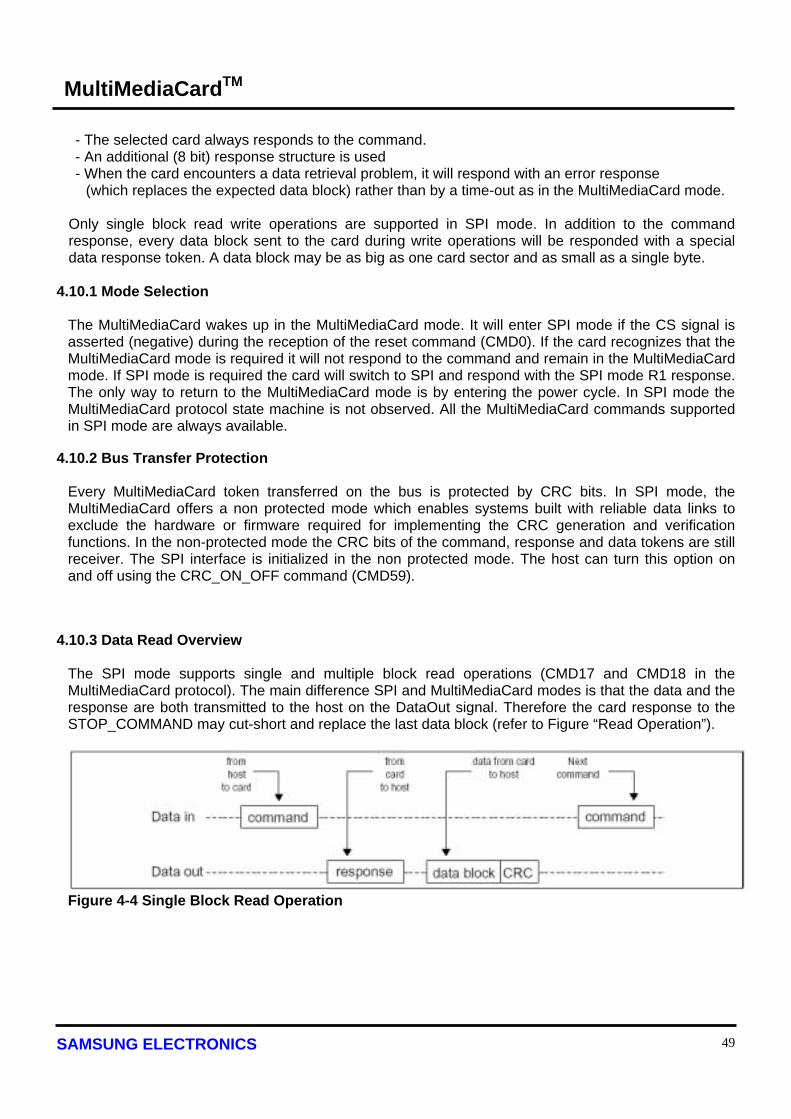
SAMSUNG ELECTRONICS 49
MultiMediaCardTM
- The selected card always responds to the command. - An additional (8 bit) response structure is used - When the card encounters a data retrieval problem, it will respond with an error response
(which replaces the expected data block) rather than by a time-out as in the MultiMediaCard mode. Only single block read write operations are supported in SPI mode. In addition to the command response, every data block sent to the card during write operations will be responded with a special data response token. A data block may be as big as one card sector and as small as a single byte.
4.10.1 Mode Selection The MultiMediaCard wakes up in the MultiMediaCard mode. It will enter SPI mode if the CS signal is asserted (negative) during the reception of the reset command (CMD0). If the card recognizes that the MultiMediaCard mode is required it will not respond to the command and remain in the MultiMediaCard mode. If SPI mode is required the card will switch to SPI and respond with the SPI mode R1 response. The only way to return to the MultiMediaCard mode is by entering the power cycle. In SPI mode the MultiMediaCard protocol state machine is not observed. All the MultiMediaCard commands supported in SPI mode are always available.
4.10.2 Bus Transfer Protection
Every MultiMediaCard token transferred on the bus is protected by CRC bits. In SPI mode, the MultiMediaCard offers a non protected mode which enables systems built with reliable data links to exclude the hardware or firmware required for implementing the CRC generation and verification functions. In the non-protected mode the CRC bits of the command, response and data tokens are still receiver. The SPI interface is initialized in the non protected mode. The host can turn this option on and off using the CRC_ON_OFF command (CMD59).
4.10.3 Data Read Overview
The SPI mode supports single and multiple block read operations (CMD17 and CMD18 in the MultiMediaCard protocol). The main difference SPI and MultiMediaCard modes is that the data and the response are both transmitted to the host on the DataOut signal. Therefore the card response to the STOP_COMMAND may cut-short and replace the last data block (refer to Figure “Read Operation”).
Figure 4-4 Single Block Read Operation

SAMSUNG ELECTRONICS 50
MultiMediaCardTM
Figure 4-5 Multiple Block Read Operation The basic unit of data transfer is a block whose maximum size is defined in the CSD (READ_BL_LEN). A 16-bit CRC is appended to the end of each block ensuring data transfer integrity (also refer to chapter “Cyclic Redundancy Check (CRC)”). CMD17 (READ_SINGLE_BLOCK) initiates a single block read. CMD18 (READ_MULTIPLE_BLOCK) starts a transfer of several consecutive blocks. Two types of multiple block read transactions are defined (the host can use either one at any time): * Open-ended Multiple block read The number of blocks for the read multiple block operation is not defined. The card willcontinuously transfer data blocks until a stop transmission command is received. * Multiple block read with pre-defined block count The card will transfer the requested number of data blocks, terminate the transaction and return to transfer state. Stop command is not required at the end of this type of multiple block read, unless terminated with an error. In order to start a multiple block read with pre-defined block count, the host must use the SET_BLOCK_COUNT command (CMD23) immediately preceding the READ_MULTIPLE_BLOCK (CMD18) command. Otherwise the card will start an open-ended multiple block read which can be stopped using the STOP_TRANSMISSION command. The host can abort reading at any time, within a multiple block operation, regardless of the its type. Transaction abort is done by sending the stop transmission command. In case of a data retrieval error, the card will not transmit any data. Instead, a special data error token will be sent to the host. Figure “Read Operation-Data Error” shows a data read operation which terminated with an error token rather than a data block.
Figure 4-6 Read operation – Data Error 4.10.4 Data Write Overview
The SPI mode supports single block and Multiple block write commands. Upon reception of a valid write command (CMD24 or CMD25), the card will respond with a response token and will wait for a data block

SAMSUNG ELECTRONICS 51
MultiMediaCardTM
to be sent from the host. CRC suffix, block length and start address restrictions are identical to the read operation (see Figure 46). If a CRC error is detected it will be reported in the data-response token and the data block will not be programmed. Every data block has a prefix of ‘Start Block’ token (one byte). After a data block has been received, the card will respond with a data-response token. If the data block has been received without errors, it will be programmed. As long as the card is busy programming, a continuous stream of busy tokens will be sent to the host (effectively holding the DataOut line low).
Figure 4-6 Single Block Write Operation In Multiple Block write operation the stop transmission will be done by sending ‘Stop Tran’ token instead of ‘Start Block’ token at the beginning of the next block.
Two types of multiple block write transactions, identical to the multiple block read, are defined (the host can use either one at any time): * Open-ended Multiple block write The number of blocks for the write multiple block operation is not defined. The card will continuously accept and program data blocks until a ‘Stop Tran’ token is received. * Multiple block write with pre-defined block count The card will accept the requested number of data blocks and terminate the transaction. ‘Stop tran’ token is not required at the end of this type of multiple block write, unless terminated with an error. In order to start a multiple block write with pre-defined block count the host must use the SET_BLOCK_COUNT command (CMD23) immediately preceding the WRITE_MULTIPLE_BLOCK (CMD25) command. Otherwise the card will start an open-ended multiple block write which can be stopped using the ‘Stop tran’ token. The host can abort writing at any time, within a multiple block operation, regardless of the its type. Transaction abort is done by sending the ‘Stop tran’ token. If a multiple block write with pre-defined block count is aborted, the data in the remaining blocks is not defined. If the card detects a CRC error or a programming error (e.g. write protect violation, out of range, address misalignment, internal error, etc.) during a multiple block write operation (both types) it will report the failure in the data-response token and ignore any further incoming data blocks. The host must than abort the operation by sending the ‘Stop Tran’ token.

SAMSUNG ELECTRONICS 52
MultiMediaCardTM
Once the programming operation is completed (either successfully or with an error), the host must check the results of the programming (or the cause of the error if already reported in the data-response token) using the SEND_STATUS command (CMD13). If the host sends a ‘Stop Trans’ token after the card received the last data block of a multiple block operation with pre-defined number of blocks, it will be interpreted as the beginning of an illegal command and responded accordingly. While the card is busy, resetting the CS signal will not terminate the programming process. The card will release the DataOut line (tri-state) and continue with programming. If the card is reselected before the programming is finished, the DataOut line will be forced back to low and all commands will be rejected. Resetting a card (using CMD0) will terminate any pending or active programming operations. This may destroy the data formats on the card. It is in the responsibility of the host to prevent it. 4.10.5 Erase and Write Protect Management
The erase and write protect management procedures in the SPI mode are identical to those of the MultiMediaCard mode. While the card is erasing or changing the write protection bits of the predefined sector list, it will be in a busy state and hold the DataOut line low. Figure “No Data Operations” illustrates a ‘no data’ bus transaction with and without busy signaling.
Figure 4-8 ‘No Data’ Operation 4.10.6 Reading CID/CSD Registers
Unlike the MultiMediaCard protocol (where the register contents are sent as a command response), reading the contents of the CSD and CID registers in SPI mode is a simple read-block transaction. The card will respond with a standard response token (refer to Figure “Read Operation”) followed by a data block of 16 bytes suffixed with a 16 bit CRC. The data timeout for the CSD command cannot be set to the card TAAC since this value is stored in the CSD. Therefore the standard response timeout value (NCR ) is used for read latency of the CSD register
4.10.7 Reset Sequence The MultiMediaCard requires a defined reset sequence. After power on reset or CMD0 (software reset) the card enters an idle state. At this state the only legal host command is CMD1 (SEND_OP_COND) and CMD58 (READ_OCR). In SPI mode, as opposed to MultiMediaCard mode, CMD1 has no operands and does not return the contents of the OCR register. Instead, the host may use CMD58 (available in SPI mode only) to read the OCR register. Furthermore, it is in the responsibility of the host to refrain from accessing cards that do not support its voltage range. The usage of CMD58 is not restricted to the initializing phase only, but can be issued at any time. The host must poll the card (by repeatedly sending CMD1) until the in-idle-state’ bit in the card response indicates (by being set to 0)

SAMSUNG ELECTRONICS 53
MultiMediaCardTM
that the card completed its initialization processes and is ready for the next command. The host must poll the card (by repeatedly sending CMD1) until the ‘in-idle-state’ bit in the card response indicates (by being set to 0) that the card completed its initialization processes and is ready for the next command.
4.10.8 Error Conditions Unlike the MultiMediaCard protocol, in the SPI mode the card will always respond to a command. The response indicates acceptance or rejection of the command. A command may be rejected if it is not supported (illegal opcode), if the CRC check failed, if it contained an illegal operand, or if it was out of sequence during an erase sequence.
4.10.9 Memory Array Partitioning Same as for MultiMediaCard mode.
4.10.10 Card Lock/Unlock Usage of card lock and unlock commands in SPI mode is identical to MultiMediaCard mode. In both cases the command response is of type R1b. After the busy signal clears, the host should obtain the result of the operation by issuing a GET_STATUS command. Please refer to Chapter “Card lock/unlock operation” for details.
4.10.11 Commands All the MultiMediaCard commands are 6 bytes long. The command transmission always starts with the left bit of the bitstring corresponding to the command codeword. All commands are protected by a CRC. The commands and arguments are listed in Table Table 4-14 Command bit position
Bit position [47] [46] [45:40] [39:8] [7:1] [0] Width (bits) 1 1 6 32 7 1 Value ‘0’ ‘1’ × × × ‘1’ Description start bit transmission bit command index argument CRC7 end bit
The following table provides a detailed description of the SPI bus commands. The responses are defined in Chapter “Responses”. The Table “Commands and Arguments” lists all MultiMediaCard commands. A “yes” in the SPI mode colon indicates that the command is supported in SPI mode. With these restrictions, the command class description in the CSD is still valid. If a command does not require an argument, the value of this field should be set to zero. The reserved commands are reserved in MultiMediaCard mode as well. The binary code of a command is defined by the mnemonic symbol. As an example, the content of the command index field is (binary) ‘000000’ for CMD0 and ‘100111’ for CMD39. Table 4-15 Commands and Arguments
CMD index SPI mode Argument Resp Abbreviation Command description CMD0 Yes None R1 GO_IDLE_STATE resets the MultiMediaCard CMD1 Yes None R1 SEND_OP_COND Activates the card’s initialization
process. CMD2 No CMD3 No

SAMSUNG ELECTRONICS 54
MultiMediaCardTM
CMD4 No CMD5 reversed CMD6 reversed CMD7 No CMD8 reversed CMD9 Yes None R1 SEND_CSD asks the selected card to send its
card-specific data (CSD) CMD10 Yes None R1 SEND_CID asks the selected card to send its
card identification (CID) CMD11 No CMD12 No CMD13 Yes None R2 SEND_STATUS asks the selected card to send its
status register. CMD14 reversed CMD15 No CMD16 Yes [31:0] block length R1 SET_BLOCKLEN selects a block length (in bytes)
for all following block commands (read and write). *1
CMD17 Yes [31:0] data address
R1 READ_SINGLE_ BLOCK
reads a block of the size selected by the SET_BLOCKLEN command. *2
CMD18 Yes [31:0] data address
R1 READ_MULTIPLE_BLOCK
continuously transfers data blocks from card to host until interrupted by a stop command or the requested number of data blocks transmitted.
CMD19 reversed CMD20 No CMD21… CMD22
reversed
CMD23 Yes [31:16] set to 0 [15:0] number of
blocks
R1 SET_BLOCK_COUNT
Defines the number of blocks which are going to be transferred in the immediately exceeding multiple block read or write command.
CMD24 Yes [31:0] data address
R1b *3 WRITE_BLOCK writes a block of the size selected by the SET_BLOCKLEN command. *4
CMD25 Yes [31:0] data address
R1 WRITE_MULTIPLE_BLOCK
continuously writes blocks of data until a “Stop Tran” Token or the requested number of blocks received.
CMD26 No CMD27 Yes None R1b PROGRAM_CSD programming of the
programmable bits of the CSD. CMD28 Yes [31:0] data
address R1b SET_WRITE_
PROT if the card has write protection features, this command sets the write protection bit of the addressed group. The properties of write protection are coded in the card specific data (WP_GRP_SIZE).
CMD29 Yes [31:0] data address
R1b CLR_WRITE_ PROT
if the card has write protection features, this command clears the write protection bit of the
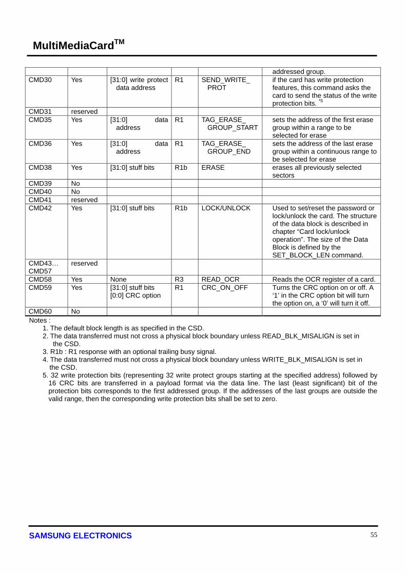
SAMSUNG ELECTRONICS 55
MultiMediaCardTM
addressed group. CMD30 Yes [31:0] write protect
data address R1 SEND_WRITE_
PROT if the card has write protection features, this command asks the card to send the status of the write protection bits. *5
CMD31 reserved CMD35 Yes [31:0] data
address R1 TAG_ERASE_
GROUP_STARTsets the address of the first erase group within a range to be selected for erase
CMD36 Yes [31:0] data address
R1 TAG_ERASE_ GROUP_END
sets the address of the last erase group within a continuous range to be selected for erase
CMD38 Yes [31:0] stuff bits R1b ERASE erases all previously selected sectors
CMD39 No CMD40 No CMD41 reserved CMD42 Yes [31:0] stuff bits R1b LOCK/UNLOCK Used to set/reset the password or
lock/unlock the card. The structure of the data block is described in chapter “Card lock/unlock operation”. The size of the Data Block is defined by the SET_BLOCK_LEN command.
CMD43… CMD57
reserved
CMD58 Yes None R3 READ_OCR Reads the OCR register of a card.CMD59 Yes [31:0] stuff bits
[0:0] CRC option R1 CRC_ON_OFF Turns the CRC option on or off. A
‘1’ in the CRC option bit will turn the option on, a ‘0’ will turn it off.
CMD60 No Notes :
1. The default block length is as specified in the CSD. 2. The data transferred must not cross a physical block boundary unless READ_BLK_MISALIGN is set in the CSD. 3. R1b : R1 response with an optional trailing busy signal. 4. The data transferred must not cross a physical block boundary unless WRITE_BLK_MISALIGN is set in the CSD. 5. 32 write protection bits (representing 32 write protect groups starting at the specified address) followed by
16 CRC bits are transferred in a payload format via the data line. The last (least significant) bit of the protection bits corresponds to the first addressed group. If the addresses of the last groups are outside the valid range, then the corresponding write protection bits shall be set to zero.

SAMSUNG ELECTRONICS 56
MultiMediaCardTM
4.10.12 Responses
There are several types of response tokens. As in the MultiMediaCard mode, all are transmitted MSB first: * Format R1 This response token is sent by the card after every command with the exception of SEND_STATUS commands. It is one byte long, and the MSB is always set to zero. The other bits are error indications, an error being signaled by a ‘1’. The structure of the R1 format is given in Figure “R1 Response Format”. The meaning of the flags is defined as following - In idle state: The card is in idle state and running the initializing process. - Erase reset: An erase sequence was cleared before executing because an out of erase sequence
command was received. - Illegal command: An illegal command code was detected. - Communication CRC error: The CRC check of the last command failed. - Erase sequence error: An error in the sequence of erase commands occurred. - Address error: A misaligned address, which did not match the block length, was used in the
command. - Parameter error: The command’s argument (e.g. address, block length) was out of the allowed
range for this card.
Figure 4-9 R1 Response Format Format R1b This response token is identical to the R1 format with the optional addition of the busy signal. The busy signal token can be any number of bytes. A zero value indicates card is busy. A non-zero value indicates the card is ready for the next command. Format R2 This response token is two bytes long and sent as a response to the SEND_STATUS command. The format is given in Figure “R2 Response Format”.

SAMSUNG ELECTRONICS 57
MultiMediaCardTM
Figure 4-10 R2 Response Format The first byte is identical to the response R1. The content of the second byte is described in the following: - Erase param: An invalid selection, sectors or groups, for erase. - Write protect violation: The command tried to write a write protected block - Card ECC failed: Card internal ECC was applied but failed to correct the data. - CC error: Internal card controller error - Error: A general or an unknown error occurred during the operation. - Write protect erase skip | lock/unlock command failed: This status bit has two functions
overloaded. It is set when the host attempts to erase a write protected sector or if a sequence or password error occurred during card lock/unlock operation.
- Card is locked: Set when the card is locked by the user. Reset when it is unlocked. Format R3 This response token is sent by the card when a READ_OCR command is received. The response length is 5 bytes (refer to Figure “R3 Response Format”). The structure of the first (MSB) byte is identical to response type R1. The other four bytes contain the OCR register.
Figure 4-11 R3 Response Format

SAMSUNG ELECTRONICS 58
MultiMediaCardTM
Data Response Every data block written to the card will be acknowledged by a data response token. It is one byte long and has the following format:
Figure 4-11 Data Response The meaning of the status bits is defined as follows: ‘010’ - Data accepted ‘101’ - Data rejected due to a CRC error. ‘110’ - Data rejected due to a Write Error. 4.10.13 Data Tokens
Read and write commands have data transfers associated with them. Data is being transmitted or received via data tokens. All data bytes are transmitted MSB first. Data tokens are 4 to (N + 3) bytes long (Where N is the data block length set using the SET_BLOCK_LENGTH Command) and have the following format :
- First byte: Start Byte
Token Type Transaction Type 7 Bit Position 0
Start Block Single Block Read 1 1 1 1 1 1 1 0
Start Block Multiple Block Read 1 1 1 1 1 1 1 0
Start Block Single Block Write 1 1 1 1 1 1 1 0
Start Block Multiple Block Write 1 1 1 1 1 1 0 0
Stop Tran Multiple Block Write 1 1 1 1 1 1 0 1
Figure 4-12 Data Tokens - Bytes 2 – (N + 1) : User data - Last two bytes: 16 bit CRC. 4.10.14 Data Error Token
If a read operation fails and the card cannot provide the required data, it will send a data error token instead. This token is one byte long and has the following format:
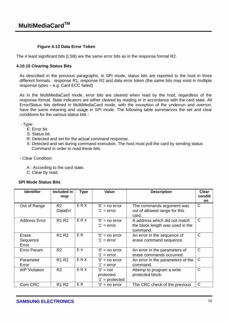
SAMSUNG ELECTRONICS 59
MultiMediaCardTM
Figure 4-13 Data Error Token The 4 least significant bits (LSB) are the same error bits as in the response format R2.
4.10.15 Clearing Status Bits
As described in the previous paragraphs, in SPI mode, status bits are reported to the host in three different formats : response R1, response R2 and data error token (the same bits may exist in multiple response types – e.g. Card ECC failed) As in the MultiMediaCard mode, error bits are cleared when read by the host, regardless of the response format. State indicators are either cleared by reading or in accordance with the card state. All Error/Status bits defined in MultiMediaCard mode, with the exception of the underrun and overrun, have the same meaning and usage in SPI mode. The following table summarizes the set and clear conditions for the various status bits :
- Type:
E: Error bit. S: Status bit.
R: Detected and set for the actual command response. X: Detected and set during command execution. The host must poll the card by sending status
Command in order to read these bits.
- Clear Condition:
A : According to the card state. C: Clear by read.
SPI Mode Status Bits
Identifier Included in resp
Type Value Description Clear conditi
on Out of Range R2
DataErr E R X ‘0’ = no error
‘1’ = error The commands argument was out of allowed range for this card.
C
Address Error R1 R2 E R X ‘0’ = no error ‘1’ = error
A address which did not match the block length was used in the command.
C
Erase Sequence Error
R1 R2 E R ‘0’ = no error ‘1’ = error
An error in the sequence of erase command sequence.
C
Error Param R2 E X ‘0’ = no error ‘1’ = error
An error in the parameters of erase commands occurred.
C
Parameter Error
R1 R2 E R X ‘0’ = no error ‘1’ = error
An error in the parameters of the command.
C
WP Violation R2 E R X ‘0’ = not protected ‘1’ = protected
Attemp to program a write protected block.
C
Com CRC R1 R2 E R ‘0’ = no error The CRC check of the previous C

SAMSUNG ELECTRONICS 60
MultiMediaCardTM
Error ‘1’ = error command failed. Illegal Command
R1 R2 E R ‘0’ = no error ‘1’ = error
Command not legal for the card state.
C
Card ECC Failed
R2 DataErr
E X ‘0’ = success ‘1’ = failure
Card internal ECC was applied but failed to correct the data.
C
CC Error R2 DataErr
E R X ‘0’ = no error ‘1’ = error
Internal card controller error. C
Error R2 DaraErr
E R X ‘0’ = no error ‘1’ = error
A general or an unknown error occurred during the operation.
C
WP Erase Skip R2 S X ‘0’ = not protected ‘1’ = protected
Only partial address space was erased due to existing WP blocks.
C
Lock/Unlock Command
R2 E X ‘0’ = no error ‘1’ = error
Sequence or password error during card lock/unlock operation.
C
Card is locked R2 DaraErr
S X ‘0’ = card is not locked ‘1’ = card is locked
Card is locked by password. A
Erase Retest R1 R2 S R ‘0’ = cleared ‘1’ = set
An erase sequence was cleared before exciting because an output of erase sequence command was received.
C
In Idle State R1 R2 S R ‘0’ = Card is ready ‘1’ = protected
The card enters the idle state after power up or reset command. It will exit this state and become ready upon completion of this initialization procedures.
A
CSD Overwrite R2 E X ‘0’ = no error ‘1’ = error
The host is trying to change the ROM section, or is trying to reserve the copy bit (set as original) or permanent WP bit (unprotected) or the CSD register.
C
4.11 SPI Bus Timing
All timing diagrams use the following schematics and abbreviations:
H Signal is high (logical ‘1’) L Transmitter bit (Host = ‘1’, Card = ‘0’) X One-cycle pull-up (= ‘1’) Z High impedance state (-> = ‘1’) * Repetition busy Busy token Command Command token Response Response token Data block Data token
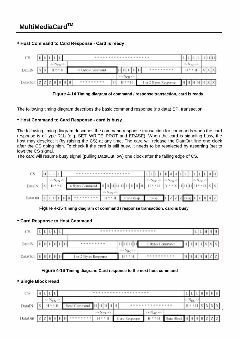
SAMSUNG ELECTRONICS 61
MultiMediaCardTM
• Host Command to Card Response - Card is ready
Figure 4-14 Timing diagram of command / response transaction, card is ready The following timing diagram describes the basic command response (no data) SPI transaction. • Host Command to Card Response - card is busy The following timing diagram describes the command response transaction for commands when the card response is of type R1b (e.g. SET_WRITE_PROT and ERASE). When the card is signaling busy, the host may deselect it (by raising the CS) at any time. The card will release the DataOut line one clock after the CS going high. To check if the card is still busy, it needs to be reselected by asserting (set to low) the CS signal. The card will resume busy signal (pulling DataOut low) one clock after the falling edge of CS.
Figure 4-15 Timing diagram of command / response transaction, card is busy • Card Response to Host Command
Figure 4-16 Timing diagram: Card response to the next host command • Single Block Read

SAMSUNG ELECTRONICS 62
MultiMediaCardTM
Figure 4-17 Timing diagram: Single block read transaction • Multiple Block Read - Stop Transmission is sent between blocks The timing for de-asserting the CS signal after the last card response is identical to a standard command/ response transaction
Figure 4-18 Timing diagram: Multiple block transaction, Stop transmission does not overlap data • Multiple Block Read - Stop Transmission is sent within a block In an Open-ended (or host aborted) multiple block read transaction the stop transmission command may be sent asynchronously to the data transmitted out of the card and may overlap the data block. In this case the card will stop sending the data and transmit the response token as well. The delay between command and response is standard NCR Clocks. The first byte, however, is not guaranteed to be all set to ‘1’. The card is allowed up to two clocks to stop data transmission. The timing for de-asserting the CS signal after the last card response is identical to a standard command/ response transaction
Figure 4-19 Timing diagram: Multiple block transaction, Stop transmission overlaps data • Reading the CSD register The following timing diagram describes the SEND_CSD command bus transaction. The time-out values between the response and the data block is NCX (Since the NAC is still unknown).

SAMSUNG ELECTRONICS 63
MultiMediaCardTM
Figure 4-20 Timing diagram: Read CSD register • Single Block Write The host may deselect a card (by raising the CS) at any time during the card busy period (refer to the given timing diagram). The card will release the DataOut line one clock after the CS going high. To check if the card is still busy it needs to be reselected by asserting (set to low) the CS signal. The card will resume busy signal (pulling DataOut low) one clock cycle after the falling edge of CS.
Figure 4-20 Timing Diagram: Single Block Write • Multiple Block Write The timimg behaviour of the multiple block write transaction starting from the comamnd up to the first data block is identical to the single block write. Figure 63 describes the timing between the data blocks of a multiple block write transaction. Timing of the ‘Stop Tran’ token is identical to a standard data block. After the “Stop Tran” token is received ny the card, the data on the DataOut line is undefined for one byte (NBR), after which a Busy token may apear. The host may deselect and reselect the card during every busy period between the data blocks. Timing for toggling the CS signal is identical to the Single block write transaction.
Figure 4-21 Timing Diagram: Multiple Block Write Timing Values
Min Max Unit NCS 0 8 8Clock cycles NCR 1 8 8Clock cycles NCX 0 8 8Clock cycles
NAC 1 (10/8)*(TAAC*Fop+100*NSAC) 8Clock cycles
NRC 1 8 8Clock cycles NWR 1 8 8Clock cycles NEC 0 8 8Clock cycles

SAMSUNG ELECTRONICS 64
MultiMediaCardTM
NDS 0 8 8Clock cycles NBR 1 1 8Clock cycles
4.12 Error Handling
MultiMediaCards are defined as error free devices or as devices with a defined maximum bit error rate (with external error correction circuitry). To correct defects in the memory field of the cards the system may include error correction codes in the payload data (ECC). This correction is intended to correct static errors. Additionally two methods of detecting errors generated during the data transfer (dynamic errors) via a cyclic redundancy check (CRC) are implemented.
4.12.1 Error Correction Code (ECC) The MultiMediaCard is free of static errors. All errors are covered inside the card, even errors occurring during the lifetime of MultiMediaCard are covered for the user. The only effect which may be notified by the end user is, that the overall memory capacity may be reduced by small number of blocks. All flash handling is done on card, so that no external error correction is needed.
4.12.2 Cyclic Redundancy Check (CRC) The intention of the ECC method is to protect the MultiMediaCard against permanent storage failures in the memory field of the card. To protect the data against errors generated during the transport over the MultiMediaCard bus dynamically, an additional feature is implemented: the cyclic redundancy check (CRC). Following the MultiMediaCard standard, the MultiMediaCard uses two different CRC codes to protect the data and the command/response transfer between card and host. Unlike the ECC, the CRC is intended only to detect transfer errors and not to correct them “on the fly”. When a CRC error is detected the host has to react. This is normally done by repeating the last command. The first CRC code is intended to protect the command and response frames. They are also used to synchronize the data stream. One CRC is checked in the MultiMediaCard for every command. For each response a CRC is generate in the MultiMediaCard. Each data block read from the MultiMediaCard will be succeeded by redundancy bits generated with the second CRC. Both CRCs are mandatory for the card and the host.
• CRC7
The CRC7 check is used for all commands, for all responses except type R3, and for the CSD and CID registers. The CRC7 is a 7-bit value and is computed as follows: generator polynomial: G(x) = x7 + x3 + 1 M(x) = (first bit) * xn + (second bit) * xn-1 +...+ (last bit) * x0 CRC[6...0] = Remainder [(M(x) * x7)/G(x)] All CRC registers are initialized to zero. The first bit is the most left bit of the corresponding bit string (of the command, response, CID or CSD). The degree n of the polynomial is the number of CRC protected bits decreased by one. The number of bits to be protected is 40 for commands and responses (n = 39), and 120 for the CSD and CID (n = 119). • CRC16 The CRC16 is used for payload protection in block transfer mode. The CRC check sum is a 16-bit value and is computed as follows:

SAMSUNG ELECTRONICS 65
MultiMediaCardTM
generator polynomial: G(x) = x16 + x12 +x5 + 1, M(x) = (first bit) * xn + (second bit) * xn-1 +...+ (last bit) * x0 CRC[15...0] = Remainder [(M(x) * x16) / G(x)] All CRC registers are initialized to zero. The first bit is the first data bit of the corresponding block. The degree n of the polynomial denotes the number of bits of the data block decreased by one (e.g. n = 4095 for a block length of 512 bytes). The generator polynomial G(x) is a standard CCITT polynomial. The code has a minimal distance d=4 and is used for a payload length of up to 2048 Bytes (n <= 16383).