Multicore SoCs stay a step ahead of SoC FPGAs · Multicore SoCs stay a step ahead of SoC FPGAs 2...
11
Multicore SoCs stay a step ahead of SoC FPGAs Punya Prakash Marketing Manager Ellen Blinka Marketing Manager Snehaprabha Narnakaje Product Manager Arnon Friedmann Business Manager Keegan Garcia Marketing Manager Robert Ferguson Business Manager & Marketing Director Texas Instruments
Transcript of Multicore SoCs stay a step ahead of SoC FPGAs · Multicore SoCs stay a step ahead of SoC FPGAs 2...

Multicore SoCs stay a step ahead of SoC FPGAs
Punya PrakashMarketing Manager
Ellen BlinkaMarketing Manager
Snehaprabha NarnakajeProduct Manager
Arnon FriedmannBusiness Manager
Keegan GarciaMarketing Manager
Robert FergusonBusiness Manager & Marketing Director
Texas Instruments

Multicore SoCs stay a step ahead of SoC FPGAs 2 March 2016
Executive summary
Historically, the differences between a system-on-a-chip (SoC) and a field programmable gate array (FPGA) were fairly obvious. Certainly there was overlap and they competed against each other in some applications, but by and large the two technologies followed their own paths. Now though, the creative marketing of FPGA vendors could suggest that they are on a collision course and are interchangeable. Nothing could be further from the truth.
Early in their evolution, FPGAs were perceived by design engineers as simply configur-able logic gates which could be applied in mundane and often repetitive operations in low-volume systems that could not justify the greater expense of an application-specific integrated circuit (ASIC). Recently, the integration of ARM® Cortex®-A cores into FPGAs and compute-intense cores could lead one to believe that the paths of true multicore SoCs and these so-called FPGA SoCs had converged. A closer examination reveals that in reality they are still very far apart and that true multicore SoCs offer increasing advantages in those critical areas required by today’s demanding products.
From FPGAs to FPGA SoCs
The first FPGAs resulted from research in the 1980s
on re-configurable computing. In the mid-80s,
patents were granted on innovations such as logic
gates, arrays and blocks. Several companies quickly
capitalized on these foundational technologies
and the FPGA industry grew rapidly. Over the
course of the 1990s and into the new century, the
capacity of FPGAs in terms of the number of gates
supported, complexity and processing speeds
advanced considerably.
When FPGAs were first created they were mostly
deployed as a replacement for discrete glue logic on
circuit boards, but as their capacities increased they
made their way into more demanding applications
in telecommunications, networking, industrial,
test and measurement, automotive, avionics and
defense, and others. The most recent evolutionary
phase for FPGAs has been to include off-the-shelf
processing cores such as one or more ARM cores
at the factory, as well as unique cores meant to
replicate digital signal processors (DSPs). The
resulting device has been called the FPGA SoC.
The clear intent of these developments has been
to position FPGAs against true multicore SoCs in
those demanding applications where over the last
decade multicore SoCs have continued to enhance
their technological advantages and increase their
market share.
While FPGA technology was evolving, multicore
SoC innovation and sophisticated architectures
were accelerating at an even faster rate. Multicore
SoCs advanced in terms of their peripherals,
interfaces, processing prowess, various on-chip
resources and a simplified way to manage data
flow and communication among resources. These
SoCs extended programming flexibility with the
inclusion of floating-point DSPs, while FPGA
vendors were using a hardened floating-point DSP,
resulting in design limitations. The expansion of
features for multicore SoCs was done with the

Multicore SoCs stay a step ahead of SoC FPGAs 3 March 2016
intent of providing the flexibility to meet the needs of
multiple markets.
As the name implies, the lofty goal of multicore
SoCs has been to place all of the resources needed
to implement a system in one device. That meant
overcoming the daunting challenges of integrating
digital logic, analog capabilities, market-required
peripherals, signal-processing cores, memory, digital
front ends (DFEs) with digital down converter-up
converter (DDUC), high-speed industry-standard
interfaces like JESD2042B and a communication
fabric so data could flow freely—all on one piece
of silicon. In addition, a significant requirement of
many system designers has been the inclusion
of several diverse types of processing units, such
as general-purpose processors (GPPs), graphical
processing units (GPU), DSPs, network processing
units (NPU), real-time processing elements such as
the programmable real-time unit (PRU-ICSS), fast
Fourier transform coprocessors (FFTCs) and others
in one system. Eventually, what was once multiple
discrete processing devices in a system evolved into
diverse processing cores integrated into a single
multicore SoC that was typically a part of a larger
SoC platform with multiple variations. If achieving all
of this was not impressive enough, the most critical
aspect of such a complex and powerful SoC are
the data paths and data flow. These become critical
when considering the wide range of markets and
applications which can be served by the same SoC/
SoC platform based on its programmability and
flexibility. Since multicore SoCs are ideal for multiple
markets, great consideration is taken during the
design phase to account for multiple data paths, and
how to pass, process, and then access the data from
multiple locations and within the multicore SoC.
Multicore SoCs have been designed with the
ability to have multiple data paths, such that data
paths can be varied based on application and
requirements. As shown in Figure 1, incoming
data to be processed can follow an almost infinite
number of flows.
Configurability, re-configurability and programmability
In certain respects, both multicore SoCs and
FPGA SoCs are configurable, re-configurable and
programmable, but the two technologies differ in
how they go about achieving each of these goals
and the degree to which each goal is achieved.
Configurability
FPGAs in general are known for their configurability.
After a lengthy development cycle, the gates
that make up an FPGA are configured to meet
the requirements of developers. In the case of
FPGA SoCs, developers would configure or insert
intellectual property (IP) blocks around the already
+* +*
–<<
DSP
ARM
Switching and I/O
Memory
ARM
...
...
+* +*
–<<
DSP
RadioAccelerationPacQueue
Manager
MulticoreNavigator
PktDMA
IndustrialAccelerationPac
CryptoAccelerationPac
PacketAccelerationPac
...
Figure 1: With multicore SoCs there are numerous datapath options. In this figure the blue arrows represent where incoming data may be sent to be stored or processed, and the black arrows show the complete accessibility of data.

Multicore SoCs stay a step ahead of SoC FPGAs 4 March 2016
integrated resources, such as the processing cores.
Some gates would be configured as data flow
channels connecting the functional blocks.
From a functional standpoint, the resources that
make up multicore SoCs are easily configurable.
Developers are able to allocate resources like
processing cores, memory, data flow channels and
others to meet system requirements. For example,
the SoC might be configured so that a certain
core that performs memory-intense operations
has dedicated memory resources and a wideband
connection to this memory while other cores share
the remaining memory.
Re-configurability
In many applications and market segments re-
configurability is just as important as configurability,
if not more so. FPGA SoCs are somewhat limited
when it comes to re-configurability. The processing
cores can be reprogrammed to operate differently
but the data flows originally configured on an
FPGA SoC can only be re-configured through a
totally new design cycle where the chip’s gates will
be re-allocated to a new architecture. Moreover,
beyond a simple daisy-chain connection, there
is no easy way to redirect or reroute the data
Get products
to market saving time in design and validation
DAYS
Software C or C++
VHDL
DFE SoC
FPGA
Software C, C++
VHDL
DSP
FPGA
Floating Pt. C, C++
Product 1 – VHDL
Product 2 – VHDL
SoC
FPGA
FPGA
Floating Pt. C, C++
Floating Pt. C, C++ Numerical Recipes Fixed-Point C
DSP
FPGA
DDUCFFTC
Algorithm
Floating-PointAlgorithm
ProductUpdatesSpinoffs
WEEKS TO MONTHS
3× F A S T E R
Figure 2: Fast time to market and product scalability enabled by software programmability with high-performance technology
Data IN
Data IN
Data OUT
Data OUT
FPGA
FPGA
DataFlowLocked
A A
B B
C C
D D
New DesignRequirements
X
Y
Figure 3: Existing data flow blocks A, B, C, and D are locked in place and the implementation of new data flow blocks X and Y are limited to being placed before or after the existing data flow

Multicore SoCs stay a step ahead of SoC FPGAs 5 March 2016
flow connections already configured on an FPGA
SoC to accommodate the addition of a new
functional block.
When new requirements are put on an existing
FPGA design, engineers are limited to adding block
elements outside of the original data flow unless
the architecture is redesigned and existing gate
resources are re-allocated. Adding to or modifying
an FPGA data flow is an inflexible and inefficient
effort; in Figure 3, existing data flow blocks A, B, C,
and D are locked in place and the implementation
of new data flow blocks X and Y are limited to being
placed before or after the existing data flow.
In contrast, multicore SoCs can be re-configured in
much the same way as they were initially configured
by simply loading new firmware and software to
allocate the chip’s resources in a different manner.
On-chip memory might be re-allocated for greater
efficiencies or the data flows adjusted to correct
unforeseen bottlenecks. Because the resources are
already on the device, re-configuring a multicore
SoC is simply a matter of allocating these resources
in a different way by updating the system’s software.
Programmability
In this regard, FPGA SoCs and multicore SoCs
are similar, as the processing cores in both are
programmable. Where multicore SoCs shine is
their programmability at the system level. Altering
the processing of the cores in an FPGA SoC is
often futile unless the system data flows can be
re-configured to accommodate the new processing
procedures. And to change the data flows, the
FPGA SoC must go through an entire development
cycle again. Unlike an FPGA SoC, the processing
cores, co-processors, accelerators and other
processing engines in an SoC can be programmed
in a relatively high-level language like C++ and the
system-level data flows can be re-defined at the
same time. In fact, the software running on cores
in an SoC has the ability to dynamically re-allocate
data channels in response to the processing load,
something an FPGA SoC would not be able to do.
Pros and Cons
System designers of high-speed data acquisition
systems in various markets will typically perform
some sort of ‘“pros and cons” evaluation of FPGA
SoCs and multicore SoCs against a number of
critical criteria such as the following.
Futureproofing is a critical consideration for several
growing markets served by multicore SoCs and
FPGAs. Essentially, futureproofing comes down
to how easily system functionality can be altered.
This can be required by updates to standards, new
technologies or re-use in another application.
Another key consideration is data flow flexibility.
Adding a functional block, for example, can often
necessitate rerouting the data flow. Multicore SoCs
typically have a wealth of on-chip data flow options
to accommodate design changes. For example,
TI’s processors based on KeyStone™ II architecture
include multiple EDMA channels and semaphores
as well as other hardware modules for data flow:
Packet DMA and queue manager. By comparison,
altering the architecture of an FPGA SoC would
trigger an entirely new design cycle.
The diversity of processors, co-processors and
accelerators is also an important consideration for
system architects. For more than a decade now,
the providers of multicore SoCs have integrated
different processor core types, co-processors
and specialized task-specific accelerators into
their heterogeneous multicore architectures.
The intricacies of core-to-core communications,
resource sharing, processing load distribution

Multicore SoCs stay a step ahead of SoC FPGAs 6 March 2016
across cores—all of these complexities and others
have been resolved by multicore SoC suppliers.
For example, TI’s software development kit (SDK)
provides tools for these multicore challenges along
with example applications. Certainly many of these
processor types are available as IP for integration into
FPGA SoCs, but the system designers themselves
would then face the challenge of resolving these
communications, collaboration and resource
allocation issues. And, in many cases, the expertise
needed to do this can be quite specialized and not
typically available on the staff of a system supplier.
Multicore SoCs based on KeyStone architecture
(Figure 4) provide developers options that are
the best of both worlds. They include multiple
programmable cores which allow for customization
and differentiation, while also providing hardware
accelerators for optimal performance for dedicated
functions. In most cases these hardware
accelerators are also software programmable.
Power consumption is a major concern in many
applications, especially mobile or thermally-
constrained systems which may require no
moving parts, for example cooling fans, for
reliability reasons. Both FPGA SoCs and multicore
SoCs typically feature low-power ARM Cortex-A
processing cores, but multicore SoCs are usually
capable of greater granularity in their adaptive
power management strategies, which are able to
shut down or scale back the operations of system
partitions to reduce power consumption further.
Many multicore SoCs are commonly released
with software to leverage the power management
features of the SoC.
Especially in embedded applications, package
size or footprint is an important criterion for system
designers. FPGA SoC packaging is significantly
larger than multicore SoC devices. Some SoCs
come in packaging as small as 12 × 12 mm ball grid
array (BGA) packages. In addition, SoCs are usually
compatible with 3D stacked packaging or package-
on-package structures.
System cost is another concern that can be
reduced in SoCs in a number of ways. The higher
levels of integration found in SoCs can consolidate
functionality that had been previously accomplished
in discrete devices. This reduces the bill of materials
(BOM) cost and printed circuit board area.
For system suppliers, the cost of any technology
cannot be measured solely by procurement costs.
Over the course of a system’s life cycle, the ease or
complexity of its design and development cycle will
also contribute cost to the product. Shorter, simpler
development cycles reduce development costs
and deliver a new system to market faster, avoiding
those opportunity costs that result from a late
product introduction. In contrast to the complexity
of the FPGA multicore SoC’s development cycle,
the resources on a multicore SoC have already been
integrated, characterized, validated and tested so
that system designers can focus on configuring the
system architecture, programming the application
with competitive advantages and introducing a
new product.
Multicore Shared
Memory Controller
011100
100010
001111
Tera
Ne
t
Multicore Navigator
+* +*
–<
DSP
CorePacs
ARM
CorePacs
Packet AccelerationPac
Industrial AccelerationPac
Radio AccelerationPac
Crypto AccelerationPac
Switching and I/O
CPRI, SRIO, Hyperlink, PCIe,
1 GbE/10 GbE, JESD204B
Figure 4: Block diagram of KeyStone architecture

Multicore SoCs stay a step ahead of SoC FPGAs 7 March 2016
Use cases
In many of today’s high-speed data acquisition
applications, which are prevalent in vertical
industries such as industrial automation, automotive,
aerospace and avionics and test and measurement,
multicore SoCs provide a system solution that can
be rapidly deployed to the marketplace yet flexible
enough to adapt to specific design requirements
and to changing demands in the industry. The use
cases briefly detailed below are specific to several of
these vertical industries and highlight the capabilities
of multicore SoCs that are particularly beneficial in
each industry.
Industrial automation
The industrial control and automation marketplace is
dominated by several older serial fieldbus standards
like PROFIBUS®, the CAN bus, Modbus® and
CC-Link® and a few relatively new real-time
Ethernet standards, including EtherCAT®,
EtherNet/IP™, PROFINET®, POWERLINK and
Sercos III. All of these standards have evolved over
several years, but they have
continued to be updated
and revised periodically.
Additionally, redundancy
layers using protocols such
as IEC 62439-3 (HSR, PRP)
are becoming more prevalent
in order to improve reception
of critical messages. As a
result, the programmability
of multicore SoCs helps
them easily adapt to future
changes, which is extremely
beneficial to industrial control
system suppliers who must be
able to adapt their equipment
to constantly changing
standards. With SoC-based systems, updates
to a standard can often be handled by a remote
software download to a real-time programmable
element, while an FPGA SoC would likely need to
be redesigned.
In addition to using software updates to upgrade
to the latest version of a protocol after a standard
is updated, multicore SoCs which integrate real-
time programmable elements are more flexible than
FPGA SoCs in that they can dynamically switch
between protocols. TI Sitara™ processors include
a PRU-ICSS, which is comprised of RISC cores
with dedicated I/O. The PRU-ICSS is capable of
detecting the type of industrial Ethernet protocol
being used in a situation, and then loading new
firmware on the fly during runtime in order to match
the detected industrial Ethernet protocol. An FPGA
SoC, where a protocol implementation has to be
hard-coded in gates, would have to have each
separate protocol coded in separate gates to realize
the same functionality. In the FPGA implementation,
having the ability to run multiple protocols
Feature/Benefit Multicore SoC FPGA SoC
Futureproofing Easily reprogrammed Redesign required
Data flow Very flexible Unchangeable without a re-design
Processor diversity Already integrated, highly programmable General-purpose cores already integrated. Additional core types available as IP, but integration and licenses required
Power consumption Low-power ARM cores, fine-grain power management strategies possible
Low-power ARM cores, no inherent power management
Footprint Small, compact, stackable packages Large footprint
System cost High integration reduces system cost and small footprint reduces PCB cost
Costly IP integration required, larger footprint requires larger PCB space
Cost of ownership Shorter development cycle and faster time-to-market
More complex development
Time-to-market Programmable resources shorten development cycles
Complex development cycle lengthens time-to-market
Table 1: Pros and cons of multicore SoCs and FPGA SoCs
Multicore SoCs stay a step ahead of SoC FPGAs 8 March 2016
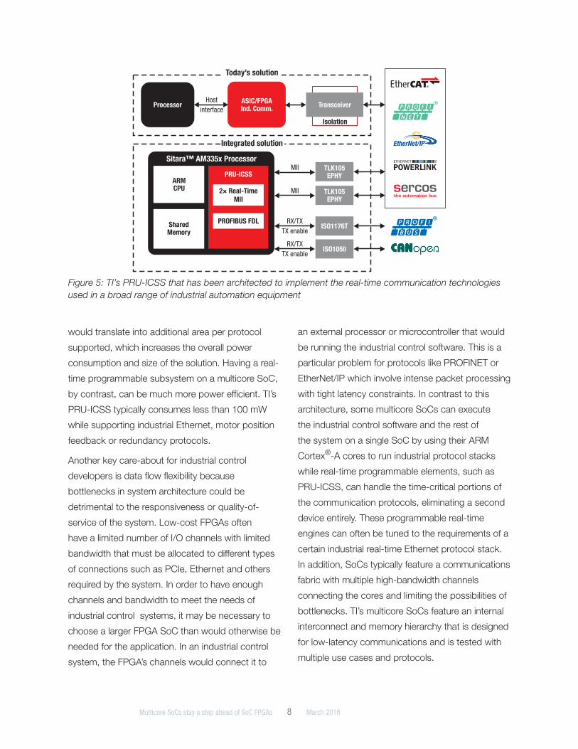
would translate into additional area per protocol
supported, which increases the overall power
consumption and size of the solution. Having a real-
time programmable subsystem on a multicore SoC,
by contrast, can be much more power efficient. TI’s
PRU-ICSS typically consumes less than 100 mW
while supporting industrial Ethernet, motor position
feedback or redundancy protocols.
Another key care-about for industrial control
developers is data flow flexibility because
bottlenecks in system architecture could be
detrimental to the responsiveness or quality-of-
service of the system. Low-cost FPGAs often
have a limited number of I/O channels with limited
bandwidth that must be allocated to different types
of connections such as PCIe, Ethernet and others
required by the system. In order to have enough
channels and bandwidth to meet the needs of
industrial control systems, it may be necessary to
choose a larger FPGA SoC than would otherwise be
needed for the application. In an industrial control
system, the FPGA’s channels would connect it to
an external processor or microcontroller that would
be running the industrial control software. This is a
particular problem for protocols like PROFINET or
EtherNet/IP which involve intense packet processing
with tight latency constraints. In contrast to this
architecture, some multicore SoCs can execute
the industrial control software and the rest of
the system on a single SoC by using their ARM
Cortex®-A cores to run industrial protocol stacks
while real-time programmable elements, such as
PRU-ICSS, can handle the time-critical portions of
the communication protocols, eliminating a second
device entirely. These programmable real-time
engines can often be tuned to the requirements of a
certain industrial real-time Ethernet protocol stack.
In addition, SoCs typically feature a communications
fabric with multiple high-bandwidth channels
connecting the cores and limiting the possibilities of
bottlenecks. TI’s multicore SoCs feature an internal
interconnect and memory hierarchy that is designed
for low-latency communications and is tested with
multiple use cases and protocols.
TLK105
EPHY
TLK105
EPHY
ISO1176T
ISO1050
2× Real-Time
MII
ARM
CPU
Shared
Memory
PRU-ICSS
PROFIBUS FDL
Sitara™ AM335x Processor
Host
interface
MII
MII
RX/TX
TX enable
RX/TX
TX enable
ProcessorASIC/FPGA
Ind. Comm.Transceiver
Isolation
Today’s solution
Integrated solution
Figure 5: TI’s PRU-ICSS that has been architected to implement the real-time communication technologies used in a broad range of industrial automation equipment

Multicore SoCs stay a step ahead of SoC FPGAs 9 March 2016
Automotive
In the automotive industry low power consumption
is a necessity in many applications such as
advanced driver assistance systems (ADAS), hybrid/
electric powertrains and others. The low-power
architectures of SoCs as well as their sophisticated
power-management capabilities are critical in these
types of applications. In addition, accelerators
and specialized processors that are available in
SoCs mean that automotive system designers can
maximize processing capabilities while minimizing
power consumption. In vision systems, for example,
engineers can employ an SoC with an embedded
vision engine (EVE) and one or more DSPs to
implement a system with optimal processing
capabilities per watt of power consumed. In
real-time systems like automotive applications,
these supplemental processing engines play a
major role in eliminating latencies and ensuring
deterministic responsiveness. Many of these
specialized processing engines are not available
as IP for integration into FPGA SoCs. A full-scale
development effort would be required to include
them in an automotive FPGA SoC.
Power management strategies are also critical for
addressing thermal issues, which often come into
play in embedded systems. For example, a rear-
view camera is typically housed in a very small
compartment. Without sensibly managing the
thermal issues in such a small space, the system
would likely overheat and become unreliable.
Futureproofing is another high priority in the
automotive industry where the introduction of
new features and functionality is often an annual
occurrence. With the programmability and
architectural re-configurability of multicore SoCs,
features can be updated or new functionality
incorporated into an existing system relatively
easily. Moreover, the ease of programming SoCs
also enables significant reuse among automotive
subsystems, reducing development and
maintenance costs as well as accelerating time-to-
market. For example, object detection functionality
developed for a high-end premium car’s front
camera system might be redeployed in the car’s
rear camera or surround view systems as well. In
addition, the scalability of a SoC-based system
would allow it to be reused in mid-range or low-end
models, too.
Functional safety is a paramount concern for
automotive engineers. Multicore SoCs have a
number of features that ensure their reliability,
including single-bit parity checks, multibit error
correcting code, redundant processors, cyclical
redundancy checking, built-in self-test for logic and
memory, and others safety features.
Aerospace and avionics
Many aerospace and avionic embedded systems
require an optimal combination of low power
consumption, system cost and sophisticated high-
speed processing. Demanding applications like
synthetic aperture radar (SAR) and phased array
radar place unique and very stringent requirements
on size, weight and power, and cost (SWaP-C), to
the point where one metric cannot be sacrificed
for another. Balancing power consumption and
processing power is challenging, but many multicore
SoCs include adaptive power management
technology that ensures the greatest processing
power per watt in a given footprint.
In addition, system costs are usually reduced
because of the high level of integration in some
SoCs. Integrating a DFE for DDUC and filtering
capabilities as well as high-speed serializer/
deserializer (SerDes) like JESD204B for interfacing
to high-speed data converters will typically reduce

system costs by as much as 50 percent and PCB
space requirements by 66 percent.
Test and measurement
The test and measurement (T&M) market is
composed of a wide range of different kinds
of systems from portable handheld devices to
rack-mounted equipment. The scalability and
futureproofing features of multicore SoCs make
them an effective solution for designers of T&M
systems, such as oscilloscopes, spectrum
analyzers, signal and logic analyzers and various
types of equipment for mechanical testing like
non-destructive testing, industrial X-rays, materials
testing and precision measurements.
Many of today’s T&M devices and equipment are
deployed in fast-paced industries like electronics,
computers and communications where the
rate of change resulting from the introduction
of new technologies can be challenging. As
a result, designers of T&M systems value the
programmability of SoCs because their systems
must be able to quickly adapt to new technologies
as they emerge. Often, T&M systems must be able
to be upgraded or enhanced through a firmware
update in the field.
Conclusions
Multicore SoCs, with their high level of off-the-shelf
functional integration are an excellent match for
the requirements of high-speed data acquisition
markets. The recent integration into SoCs of digital
front ends, diverse and often specialized processing
cores, high-speed serial interfaces like JESD204B,
PCI Express, Gigabit Ethernet, USB and SPI, and
other system resources simplifies system designs
and enables a truly futureproof implementation.
While FPGA SoC vendors have improved their
offerings by integrating cores to mimic a true
multicore SoC, these two types of devices actually
remain far apart. True multicore SoCs maintain a
substantial lead in terms of their ready-to-deploy
and easily programmable processing functionality,
high-bandwidth data flow resources, an extensive
list of processing engines, co-processors and
accelerators, on-chip peripherals interfaces and
much more. This is especially true in certain market
segments that place a premium on high-speed
data acquisition and powerful processing, such
as industrial automation and control, automotive,
aerospace and avionics, and test and measurement.
SPRY296© 2016 Texas Instruments Incorporated
Important Notice: The products and services of Texas Instruments Incorporated and its subsidiaries described herein are sold subject to TI’s standard terms and conditions of sale. Customers are advised to obtain the most current and complete information about TI products and services before placing orders. TI assumes no liability for applications assistance, customer’s applications or product designs, software performance, or infringement of patents. The publication of information regarding any other company’s products or services does not constitute TI’s approval, warranty or endorsement thereof.
The platform bar, KeyStone and Sitara are trademarks of Texas Instruments. All other trademarks are the property of their respective owners.

IMPORTANT NOTICE
Texas Instruments Incorporated and its subsidiaries (TI) reserve the right to make corrections, enhancements, improvements and otherchanges to its semiconductor products and services per JESD46, latest issue, and to discontinue any product or service per JESD48, latestissue. Buyers should obtain the latest relevant information before placing orders and should verify that such information is current andcomplete. All semiconductor products (also referred to herein as “components”) are sold subject to TI’s terms and conditions of salesupplied at the time of order acknowledgment.TI warrants performance of its components to the specifications applicable at the time of sale, in accordance with the warranty in TI’s termsand conditions of sale of semiconductor products. Testing and other quality control techniques are used to the extent TI deems necessaryto support this warranty. Except where mandated by applicable law, testing of all parameters of each component is not necessarilyperformed.TI assumes no liability for applications assistance or the design of Buyers’ products. Buyers are responsible for their products andapplications using TI components. To minimize the risks associated with Buyers’ products and applications, Buyers should provideadequate design and operating safeguards.TI does not warrant or represent that any license, either express or implied, is granted under any patent right, copyright, mask work right, orother intellectual property right relating to any combination, machine, or process in which TI components or services are used. Informationpublished by TI regarding third-party products or services does not constitute a license to use such products or services or a warranty orendorsement thereof. Use of such information may require a license from a third party under the patents or other intellectual property of thethird party, or a license from TI under the patents or other intellectual property of TI.Reproduction of significant portions of TI information in TI data books or data sheets is permissible only if reproduction is without alterationand is accompanied by all associated warranties, conditions, limitations, and notices. TI is not responsible or liable for such altereddocumentation. Information of third parties may be subject to additional restrictions.Resale of TI components or services with statements different from or beyond the parameters stated by TI for that component or servicevoids all express and any implied warranties for the associated TI component or service and is an unfair and deceptive business practice.TI is not responsible or liable for any such statements.Buyer acknowledges and agrees that it is solely responsible for compliance with all legal, regulatory and safety-related requirementsconcerning its products, and any use of TI components in its applications, notwithstanding any applications-related information or supportthat may be provided by TI. Buyer represents and agrees that it has all the necessary expertise to create and implement safeguards whichanticipate dangerous consequences of failures, monitor failures and their consequences, lessen the likelihood of failures that might causeharm and take appropriate remedial actions. Buyer will fully indemnify TI and its representatives against any damages arising out of the useof any TI components in safety-critical applications.In some cases, TI components may be promoted specifically to facilitate safety-related applications. With such components, TI’s goal is tohelp enable customers to design and create their own end-product solutions that meet applicable functional safety standards andrequirements. Nonetheless, such components are subject to these terms.No TI components are authorized for use in FDA Class III (or similar life-critical medical equipment) unless authorized officers of the partieshave executed a special agreement specifically governing such use.Only those TI components which TI has specifically designated as military grade or “enhanced plastic” are designed and intended for use inmilitary/aerospace applications or environments. Buyer acknowledges and agrees that any military or aerospace use of TI componentswhich have not been so designated is solely at the Buyer's risk, and that Buyer is solely responsible for compliance with all legal andregulatory requirements in connection with such use.TI has specifically designated certain components as meeting ISO/TS16949 requirements, mainly for automotive use. In any case of use ofnon-designated products, TI will not be responsible for any failure to meet ISO/TS16949.
Products ApplicationsAudio www.ti.com/audio Automotive and Transportation www.ti.com/automotiveAmplifiers amplifier.ti.com Communications and Telecom www.ti.com/communicationsData Converters dataconverter.ti.com Computers and Peripherals www.ti.com/computersDLP® Products www.dlp.com Consumer Electronics www.ti.com/consumer-appsDSP dsp.ti.com Energy and Lighting www.ti.com/energyClocks and Timers www.ti.com/clocks Industrial www.ti.com/industrialInterface interface.ti.com Medical www.ti.com/medicalLogic logic.ti.com Security www.ti.com/securityPower Mgmt power.ti.com Space, Avionics and Defense www.ti.com/space-avionics-defenseMicrocontrollers microcontroller.ti.com Video and Imaging www.ti.com/videoRFID www.ti-rfid.comOMAP Applications Processors www.ti.com/omap TI E2E Community e2e.ti.comWireless Connectivity www.ti.com/wirelessconnectivity
Mailing Address: Texas Instruments, Post Office Box 655303, Dallas, Texas 75265Copyright © 2016, Texas Instruments Incorporated