Multi-Williams FPGA - Carnegie Mellon...
33
1 Multi-Williams FPGA Sean Coleman, Tom Tzou, Joon Ho Cho
Transcript of Multi-Williams FPGA - Carnegie Mellon...
1
Multi-Williams FPGA
Sean Coleman, Tom Tzou, Joon Ho Cho
2
Table of Contents
Project Description.......................................................................................................................... 3
Design Overview/Partitioning ........................................................................................................ 4
System Overview ............................................................................................................................ 6
MPU (M6809E)........................................................................................................................... 7
MPU Memory Map ..................................................................................................................... 9
Video Processing: Video Translation Layer ............................................................................ 10
Video Hardware: CRT Emulation – Pixel Gun Position........................................................... 11
Video Hardware: Special Chip (SC1) ....................................................................................... 12
6821 PIA ................................................................................................................................... 14
User Input (Arcade Controls) .................................................................................................... 16
Sound ......................................................................................................................................... 17
Additional Software – Menu/ROM Loading ............................................................................ 18
EDK BRAM .............................................................................................................................. 19
Testing Procedure ......................................................................................................................... 21
Results & Conclusions .................................................................................................................. 23
Individual Reports ......................................................................................................................... 24
User Controls - Digilent Pinout & UCF Constraints: ................................................................... 31
Sources .......................................................................................................................................... 33
3
Project Description
Our project involved supporting playable versions of the early 1980’s classic arcade
games, Joust, Robotron, Stargate and Defender. Defender and Stargate were both side-scrolling
shooters that used only the simplest hardware and differed only by their memory-mapping
schemes. Joust and Robotron, however, were rather different. Though both used a new DMA
chip to speed up graphics routines, Joust provided simultaneous two-player support, in a game in
which riders attempted to knock their opponents off flying ostriches, while Robotron was a
single-player only game in which both joysticks were used for movement and shooting.
Despite the apparent differences, there were enough similarities in the architecture to
make a multigame implementation feasible. Defender’s memory mapping was the largest
difference, due to it being Williams Electronics’ first arcade game. Stargate, Joust and Robotron
shared the same memory setup, with Joust and Robotron only being ROM swaps, and only the
inclusion of the DMA chip differentiated the game.
Our plan was to use the PowerPC to display a menu, as well as selectively enable/disable
hardware in order to support the games without the need to reflash, a problem that other groups,
such as the NES of the past three years, had ran into. On startup, the menu would let the user
cycle through the game, and then load the necessary ROMs into the correct location before
allowing our processor to run.
4
Design Overview/Partitioning
MPU: The main processing unit, this processor runs the main game code and controls all of the
other devices via memory-mpaped I/O attached to the single data bus.
--Design: Sean Coleman
--Testing: Sean Coleman & Thomas Tzou
Memory Map: This unit translates the CPU address into the correct format for accessing the
EDK BRAMs, as well as muxing in the PIAs and sound ―bus‖ as necessary.
--Design: Sean Coleman
--Testing: Sean Coleman & Thomas Tzou
Video Translation Layer: This piece of software scans the Williams framebuffer and generates
a converted version for display on the VGA screen.
--Design: Joon Ho Cho
--Testing: Joon Ho Cho
CRT Timing/Pixel Gun: Williams was able to access the actual values of the pixel guns in
order to generate interrupts based on the Y-coordinate. This module replicates the necessary
hardware.
--Design: Sean Coleman & Thomas Tzou
--Testing: Sean Coleman & Thomas Tzou
Special Chip: A custom DMA unit designed by Williams, this device allows for rapid memory
movement and some specific functions.
--Design: Thomas Tzou
--Testing: Thomas Tzou (Incomplete)
5
Sound/Input PIAs: These devices handle asynchronous data transfer as well as provide
memory-mapped I/O.
--Design: Thomas Tzou
--Testing: Thomas Tzou
User Input: Custom fabricated arcade control panel with Digilent Expansion Port-compatible
interface.
--Design: Sean Coleman
--Implementation/Testing: Thomas Tzou & Joon Ho Cho
Sound CoProcessor: The original hardware design uses a 6802 processor to dynamically
generate the sound effects. We replace this device using the PowerPC core.
--Design: Sean Coleman & Joon Ho Cho
--Testing: Sean Coleman
BRAM: This module stores the program code, internal framebuffer, and scrtachpad RAM.
While Williams only uses 96kB of ROM+RAM, we generate a 128kB block due to Xilinx’s
restrictions.
--Design: Sean Coleman
--Testing: Sean Coleman & Thomas Tzou
Glue Verilog: Assorted modules that linked everything together and provided extra custom
muxing and other features as needed.
--Design: Sean Coleman & Thomas Tzou
--Testing: Sean Coleman & Thomas Tzou
6
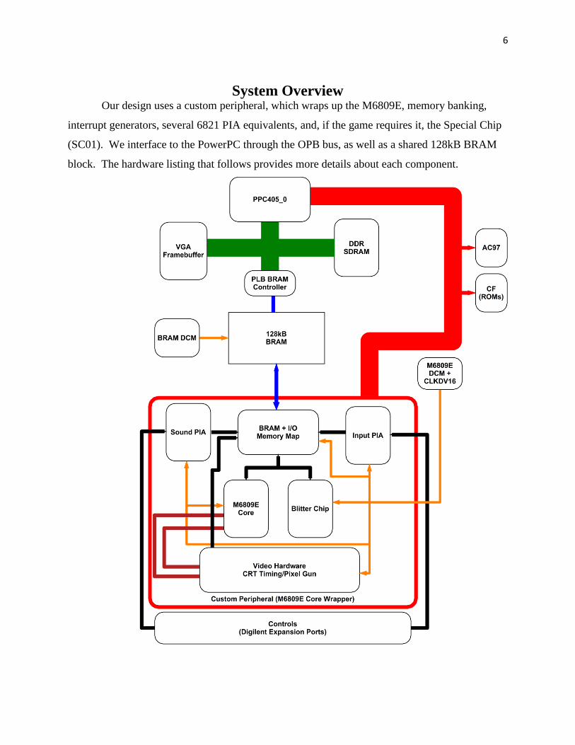
System Overview Our design uses a custom peripheral, which wraps up the M6809E, memory banking,
interrupt generators, several 6821 PIA equivalents, and, if the game requires it, the Special Chip
(SC01). We interface to the PowerPC through the OPB bus, as well as a shared 128kB BRAM
block. The hardware listing that follows provides more details about each component.
7
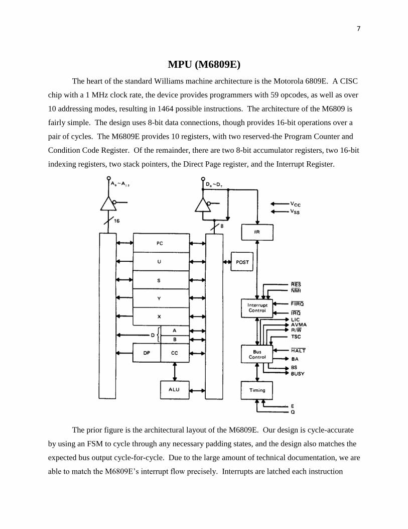
MPU (M6809E)
The heart of the standard Williams machine architecture is the Motorola 6809E. A CISC
chip with a 1 MHz clock rate, the device provides programmers with 59 opcodes, as well as over
10 addressing modes, resulting in 1464 possible instructions. The architecture of the M6809 is
fairly simple. The design uses 8-bit data connections, though provides 16-bit operations over a
pair of cycles. The M6809E provides 10 registers, with two reserved-the Program Counter and
Condition Code Register. Of the remainder, there are two 8-bit accumulator registers, two 16-bit
indexing registers, two stack pointers, the Direct Page register, and the Interrupt Register.
The prior figure is the architectural layout of the M6809E. Our design is cycle-accurate
by using an FSM to cycle through any necessary padding states, and the design also matches the
expected bus output cycle-for-cycle. Due to the large amount of technical documentation, we are
able to match the M6809E’s interrupt flow precisely. Interrupts are latched each instruction
8
fetch cycle and are only serviced if the mask bit is not set. Due to the variable length of certain
instructions, it may take up to 20 cycles before an interrupt is serviced, however, under most
cases, interrupts are serviced with 5 cycles. From Williams’ hardware documentation, we can
find that IRQ pulses are held for extremely long periods of time, at a minimum, 100 cycles,
which allows for interrupts to always be caught regardless of the current instruction being
processed. Servicing consists of pushing the current state onto the stack, then vectoring to one of
several locations based on two consecutive bytes of memory ranging from FFF0-FFFF. The
interrupts consist of IRQ/FIRQ, both of which can be masked by CC register bits, NMI, SWI,
SWI2, and SWI3, all of which are reserved opcodes, RESET, and a reserved custom Motorola
interrupt. Of these, we support IRQ, SWI, SWI2, and SWI3, as FIRQ, NMI, and RESET are all
tied high in the arcade schematics.
The primary differences between our design and that of Motorola lie in our moving the
PC and CC registers outside of the register file, primarily for convenience’s sake due to this style
matching that of a MIPS processor. Additionally, instead of a quadrature clocking scheme to
handle latching data coming in on the bus, we instead use a single 1 MHz clock and a
combinatorial bus. As a result, we clock our synchronous RAM at a 4x rate relative to the MPU
in order to keep the processors functionally identical. Furthermore, several of the output control
signals, such as the BUSY output, are left floating in the Williams design—we omit these signals
in our design. Finally, our design is 16-bit internally with 8-bit and single-bit masking support,
in contrast to the M6809E 8-bit design with extra cycles for 16-bit operations.
9
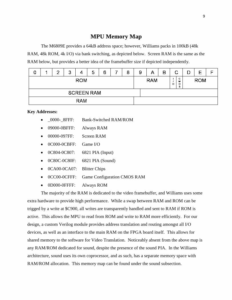
MPU Memory Map
The M6809E provides a 64kB address space; however, Williams packs in 100kB (48k
RAM, 48k ROM, 4k I/O) via bank switching, as depicted below. Screen RAM is the same as the
RAM below, but provides a better idea of the framebuffer size if depicted independently.
Key Addresses:
_0000-_8FFF: Bank-Switched RAM/ROM
09000-0BFFF: Always RAM
00000-097FF: Screen RAM
0C000-0CBFF: Game I/O
0C804-0C807: 6821 PIA (Input)
0C80C-0C80F: 6821 PIA (Sound)
0CA00-0CA07: Blitter Chips
0CC00-0CFFF: Game Configuration CMOS RAM
0D000-0FFFF: Always ROM
The majority of the RAM is dedicated to the video framebuffer, and Williams uses some
extra hardware to provide high performance. While a swap between RAM and ROM can be
trigged by a write at $C900, all writes are transparently handled and sent to RAM if ROM is
active. This allows the MPU to read from ROM and write to RAM more efficiently. For our
design, a custom Verilog module provides address translation and routing amongst all I/O
devices, as well as an interface to the main RAM on the FPGA board itself. This allows for
shared memory to the software for Video Translation. Noticeably absent from the above map is
any RAM/ROM dedicated for sound, despite the presence of the sound PIA. In the Williams
architecture, sound uses its own coprocessor, and as such, has a separate memory space with
RAM/ROM allocation. This memory map can be found under the sound subsection.
10
Video Processing:
Video Translation Layer
The Williams architecture provides no dedicated chips for video processing, other than
the blitter, explained in the next section. Physically, the game screen displays an 8-bit, 292x240
picture at 60 Hz. Internally, however, the framebuffer is extremely different. The system
actually has a 304x256 pixel framebuffer, with each pixel represented as a nibble. Each nibble
represents an offset into a 16-color palette, stored at $C000-$C00F. These 8-bit colors are split
into a 3-3-2 format:
Pal[7:6] = Blue
Pal[5:3] = Green
Pal[2:0] = Red
In order to display video through the Xilinx framebuffer, we implemented a video
translation layer that reads the Williams frame from memory, performs a conversion, and then
writes to the Xilinx framebuffer. The process, based on the MAME source code, is notated in
greater detail below:
1. Read from color palette and cache the colors into an array.
2. Read the 304 x 256 pixels from memory location 0000 to 97FF.
3. Convert each pixel into 8-bit color using the cached color palette array.
4. Translate from 8-bit color into 24-bit color.
5. Interpolate each pixel into four pixels.
6. Store the translated 24-bit color into the correct locations in the frame buffer.
Due to the PowerPC being limited to 300 MHz, while MAME benefits from much faster
processors, our translation routines are optimized, using some convenient properties of the screen
layout in order to perform the actual translation faster.
11
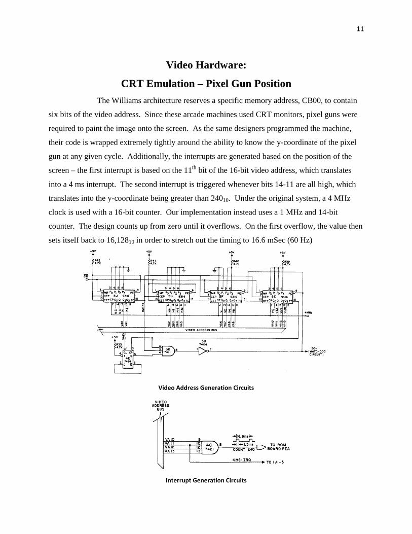
Video Hardware:
CRT Emulation – Pixel Gun Position
The Williams architecture reserves a specific memory address, CB00, to contain
six bits of the video address. Since these arcade machines used CRT monitors, pixel guns were
required to paint the image onto the screen. As the same designers programmed the machine,
their code is wrapped extremely tightly around the ability to know the y-coordinate of the pixel
gun at any given cycle. Additionally, the interrupts are generated based on the position of the
screen – the first interrupt is based on the 11th
bit of the 16-bit video address, which translates
into a 4 ms interrupt. The second interrupt is triggered whenever bits 14-11 are all high, which
translates into the y-coordinate being greater than 24010. Under the original system, a 4 MHz
clock is used with a 16-bit counter. Our implementation instead uses a 1 MHz and 14-bit
counter. The design counts up from zero until it overflows. On the first overflow, the value then
sets itself back to 16,12810 in order to stretch out the timing to 16.6 mSec (60 Hz)
Video Address Generation Circuits
Interrupt Generation Circuits
12
Video Hardware:
Special Chip (SC1)
The Williams Arcade Machines incorporated a Special Chip in the games that
followed Defender and Stargate. These special chips, also known as the blitter chips, were used
to move blocks of memory without the assistance of the MPU. They operated with just the
source address, destination address, width of the block, and height of the block. Running at an
approximated 4 MHz, a blitter chip can move around 1 million bytes per second, which is a lot
faster than relying on the MPU to move the block. These chips were generally used for quick
movements of images on the screen such as a shift of an image by just one pixel, which cut down
on the amount of ROM memory needed for sprites. The address space used for the blitter chips
was located at memory location $CA00-CA07. These locations contained the following
information:
$CA00 – Triggers the blit and provides the following control signals for the operation:
- CA00[0]: Indicates either linear or screen format, in reference to the source
data’s representation. Linear mode refers to packed data, whereas screen
format has pixel pairs separated by 256 bytes
- CA00[1]: Indicates which of the previous formats the destination data is laid
out in
- CA00[2]: Indicates if the X coordinate wraps around
- CA00[3]: Only blit the foreground (Transparency Mode)
- CA00[4]: Blit using the color mask (Solid Mode)
- CA00[5]: Rotate one pixel right. This mode shifts the image one pixel to the
right and the pixel pushed off screen is written to the left.
- CA00[6]: Blit even pixels of the block
- CA00[7]: Blit odd pixels of the block
$CA01 – Blit Mask. Usually $FF perform high-speed move of a block
$CA02 – Source Address Upper Byte
$CA03 – Source Address Lower Byte
$CA04 – Destination Address Upper Byte
$CA05 – Destination Address Lower Byte
13
$CA06 – Data Block Width
$CA07 – Data Block Height
The blitter chips will only blit when the MPU writes to address $CA00. Once triggered,
the chip asserts HALT on the MPU while it blits the indicated block. Once the blit is done,
HALT is deasserted, and processing resumes. Physically, each Williams game used two blitters,
each operating in parallel on a single pixel (4 bits); however, our implementation follows the
techniques used in the MAME source code, as well as general knowledge of what can be feasibly
implemented and thus combines the chips to a single 8-bit device.
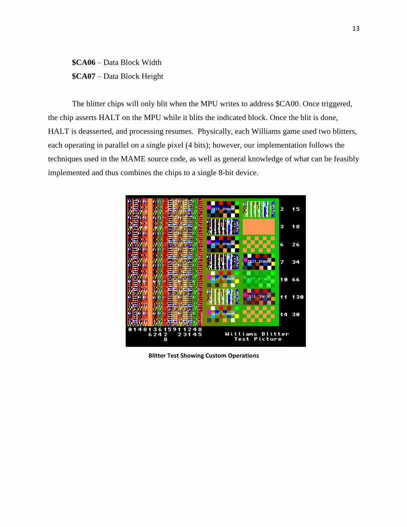
Blitter Test Showing Custom Operations
14
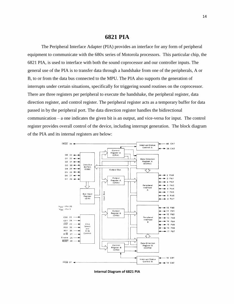
6821 PIA
The Peripheral Interface Adapter (PIA) provides an interface for any form of peripheral
equipment to communicate with the 680x series of Motorola processors. This particular chip, the
6821 PIA, is used to interface with both the sound coprocessor and our controller inputs. The
general use of the PIA is to transfer data through a handshake from one of the peripherals, A or
B, to or from the data bus connected to the MPU. The PIA also supports the generation of
interrupts under certain situations, specifically for triggering sound routines on the coprocessor.
There are three registers per peripheral to execute the handshake, the peripheral register, data
direction register, and control register. The peripheral register acts as a temporary buffer for data
passed in by the peripheral port. The data direction register handles the bidirectional
communication – a one indicates the given bit is an output, and vice-versa for input. The control
register provides overall control of the device, including interrupt generation. The block diagram
of the PIA and its internal registers are below:
Internal Diagram of 6821 PIA
15
The PIA would either take the PIA A (PA) port or the PIA B (PB) port and communicate
it with the Data Bus where the direction of communication (input or output) is determined by the
Data Direction Register (DDR). The Control Register (CR) is used to change whether the data
bus is communicating with the DDR or the PA. It is also used to generate the interrupts, CA2,
and CB2 bits. These signals were dependent on the value of certain wires and their transitions to
the values.
When trying to hook up our Verilog version of the PIA, we ran into some issues
synthesizing inouts at the top level. Old Usenet postings indicated that designers usually
replaced PIAs with sampling registers once they were used to interfacing the chips. As a result,
we rewrote our version of the PIA only operate as an input, with a separate dedicated register
handling the necessary operations on a write to the PIA to swap player controls. Due to the need
for separate functionality by the Sound and Input PIAs, we wrote two custom versions. For
input, we only needed PA and PB, as well as the control register B, as CB2 is used to select the
current player’s controls. Due to our sound implementation primarily relying on the PowerPC
and AC97 IP core, we were able to strip out all the registers except for the inputs. On the Sound
PIA, no muxes for controls exist, so we could further reduce the design to only containing two
registers. Our version was tested in simulation and was verified physically working when we ran
into the operator check screen, where we could test the advance button.
16
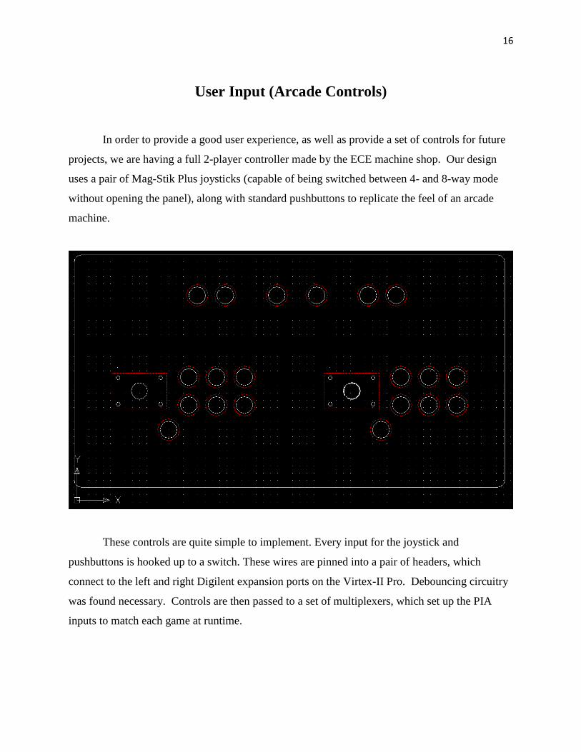
User Input (Arcade Controls)
In order to provide a good user experience, as well as provide a set of controls for future
projects, we are having a full 2-player controller made by the ECE machine shop. Our design
uses a pair of Mag-Stik Plus joysticks (capable of being switched between 4- and 8-way mode
without opening the panel), along with standard pushbuttons to replicate the feel of an arcade
machine.
These controls are quite simple to implement. Every input for the joystick and
pushbuttons is hooked up to a switch. These wires are pinned into a pair of headers, which
connect to the left and right Digilent expansion ports on the Virtex-II Pro. Debouncing circuitry
was found necessary. Controls are then passed to a set of multiplexers, which set up the PIA
inputs to match each game at runtime.
17
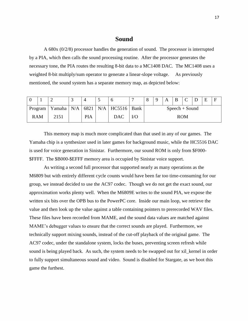
Sound
A 680x (0/2/8) processor handles the generation of sound. The processor is interrupted
by a PIA, which then calls the sound processing routine. After the processor generates the
necessary tone, the PIA routes the resulting 8-bit data to a MC1408 DAC. The MC1408 uses a
weighted 8-bit multiply/sum operator to generate a linear-slope voltage. As previously
mentioned, the sound system has a separate memory map, as depicted below:
0 1 2 3 4 5 6 7 8 9 A B C D E F
Program
RAM
Yamaha
2151
N/A 6821
PIA
N/A HC5516
DAC
Bank
I/O
Speech + Sound
ROM
This memory map is much more complicated than that used in any of our games. The
Yamaha chip is a synthesizer used in later games for background music, while the HC5516 DAC
is used for voice generation in Sinistar. Furthermore, our sound ROM is only from $F000-
$FFFF. The $B000-$EFFF memory area is occupied by Sinistar voice support.
As writing a second full processor that supported nearly as many operations as the
M6809 but with entirely different cycle counts would have been far too time-consuming for our
group, we instead decided to use the AC97 codec. Though we do not get the exact sound, our
approximation works plenty well. When the M6809E writes to the sound PIA, we expose the
written six bits over the OPB bus to the PowerPC core. Inside our main loop, we retrieve the
value and then look up the value against a table containing pointers to prerecorded WAV files.
These files have been recorded from MAME, and the sound data values are matched against
MAME’s debugger values to ensure that the correct sounds are played. Furthermore, we
technically support mixing sounds, instead of the cut-off playback of the original game. The
AC97 codec, under the standalone system, locks the buses, preventing screen refresh while
sound is being played back. As such, the system needs to be swapped out for xil_kernel in order
to fully support simultaneous sound and video. Sound is disabled for Stargate, as we boot this
game the furthest.
18
Additional Software – Menu/ROM Loading
On initialization, our system displays a simple bitmap-based menu system that allows the
user to cycle through games. Our first function polls the GPIO bus to check joystick status and
swaps bitmaps on screen to inform the player of controls. When the player presses start, the
menu returns the number of the game selected. At this point, rom_load(GAME) is called, which
mounts the Compact Flash card, selects the appropriate set of decoder PROMs, 12 program
ROMs, and a sound ROM, and then loads the data into the shared BRAM. The software then
enters a loop, where it checks for sounds to play and then sleeps. Every thirteen milliseconds,
the design also calls draw_screen(), which copies from the EDK BRAMs, deciphers the internal
framebuffer, and draws it to the screen. On every loop, the GPIO is also polled to check for the
pressing of the restart button. At this point, the custom M6809E IP is reset, the shared BRAMs
are cleared, and the processor returns to the menu loop, allowing the user to select a new game.
19
EDK BRAM
Probably the most unique portion of our project is our incorporation of a shared EDK
BRAM. The following section provides a technical overview of how the EDK fits into the
architecture, as well as provides the additional detail that the TAs had requested for use next
year. In our system, the BRAMs serve as the ROM and RAM. Instead of the traditional
approach of initializing the BRAMs during synthesis, we instead wanted the flexibility of
loading the ROMs on the fly from a menu. The FPGA primitive abstracted by the BRAM IP
provides a dual-port synchronous interface. As such, we can expose one side to the PLB bus
using a Xilinx IP. In order to hook up the other side; however, requires diving into several
different files. First, by examining the MPD, we find the necessary PORTs that need to be
exposed via the MHS file. In our design, the first port, Port A, is connected to the PLB Bus
Interface, while Port B’s internal connections are exposed:
BEGIN bram_block
PARAMETER INSTANCE = RAM
PARAMETER HW_VER = 1.00.a
BUS_INTERFACE PORTA = RAM_CNTRL_PORTA
PORT BRAM_Rst_B = mem_rst
PORT BRAM_Clk_B = mem_clk_bram
PORT BRAM_EN_B = mem_en
PORT BRAM_WEN_B = mem_wen
PORT BRAM_Addr_B = mem_addr
PORT BRAM_Din_B = mem_din
PORT BRAM_Dout_B = mem_dout
END
In our custom IP, we expose the respective lines from the correct modules as top-level ports, and
then wire the modules together. At this point, the modules are hooked up; however, there are
still several more key details that Xilinx’s documentation does not mention. First, the width of
the BRAM bus, normally user selectable, is overridden to 64 bits as soon as any bus interface is
connected to either port. The address bus, likewise, becomes 32 bits. The data bus then behaves
20
logically – for a single byte write, the user’s IP should replicate the byte 8 times, then mask out
the byte to its correct respective location.
The address port, however, is much more complicated. First, all addresses must be 8-
byte aligned. As a result, on a read, the entire line of eight addresses is returned, and the user IP
must mux out the correct byte. For writes, the lowest three bits of the user address select the
write enable signal, while the data is replicated 8 times, as previously mentioned. Due to bit
flipping depending on the endianness of the user-design, our muxing schemes have been omitted;
however, the code is clearly laid out in our custom pcore in the attached zip file. The address
bus, however, has yet another quirk, one that no documentation ever seems to mention. If the
user browses into the <PROJECT_FOLDER>\hdl\elaborate folder, there should be a folder for
each BRAM block added to the design. At the bottom of each of these directories, there is a
Verilog file containing the actual code for the primitives. If a User IP connects to the address
bus solely by padding the address with leading zeros, the design will likely not work. Upon
examining the file, the user should find the bit slice form the address port used internally. In the
case of a 128 kB BRAM block, the address is defined as BRAM_ADDR_B[15:28]. Unlike the
data ports in the design, which internally are swapped from [0:63] to [63:0], the address port is
left alone.
The elaborate file also points out the primary caveat of using BRAMs in this manner,
especially on the Virtex-II Pro. Due to architectural limitations, each BRAM block only holds a
single bit of data, and the design replicates 64 RAMB16 blocks, leading to an extremely high
cost due to the need for single-byte access while still connecting to the 64-bit PLB bus. With the
move to the new Virtex-5 boards, however, some of this cost may be mitigated due to
architectural changes to the BRAMs.
21
Testing Procedure
MPU:
Since writing machine code by hand would take far too long to test the processor, the first
goal was to find an assembler. While GCC6809, at http://www.oddchange.com/gcc6809/,
looked promising, especially since we could write more complex C code, the project’s makefile
was broken. This was replaced with the AS6809 Assembler, one of several assemblers in the
ASXXXX Cross-Assembler Project, a project run by the physics department at Kent State.
Initial tests were then written that used a set of custom Perl and TCL scripts to generate the
proper files for readmemh(), run the simulation, parse the resulting dump, and compare it to
hand-calculated results. This process was used for the majority of the operations, with only
some of the more obscure modes that we could not access through the assembler being done by
hand and using ModelSim itself to step through the code. After verifying the majority of the
modes and operations, testing continued by running both our simulation, using a custom-
assembled version of Stargate’s ROM files, and the debugger in MAME. The process primarily
consisted of tracing the code by hand on paper, finding loops where the code would return, then
setting breakpoints at these loops and comparing memory and register values. This was a bit
tricky at first since we did not use the memory completely the same way MAME had used it.
Once we got the processor to the boot screen, we moved to a combined synthesis/simulation
debugging method, where we would usually have a build of the code running on the board with
ChipScope to probe the values, and simulation running to check fixes. After we thought we had
a new working version, we would synthesize the version and continue the debug under
simulation. Our final bug, which took over 15 million cycles, eventually resulted in us finding
out that the MPU was completely working, but the interrupt timings were off.
Video:
As the Williams format for the framebuffer is documented, we first wrote a simple set
memory dump file that contained a series of rectangles. Once the parser could correctly draw
this to the screen, Sean modified the MAME source code in order to get access to the hidden
framebuffer. Dumps from different games at different points were then used to verify that the
22
video translation layer could indeed handle the Williams framebuffer format, as our rectangle
test may have been wrong.
Other Chips:
Most of our other chips had datasheets with signal timings and documented operation. After
designing the Verilog, ModelSim simulations were first used to verify proper operation, after
which a simple synthesis with some form of testing with ChipScope would then be used to verify
the design.
BRAMs:
Since the BRAMs were a rather odd portion of the design, we first did some initial testing to
make sure that we could use the BRAMs as a shared buffer. The test consisted of a four state
FSM that would do a RESET-WRITE-NOP-READ at address 0, while the PowerPC would poll
address 0. When the PowerPC finally caught the correct value, and ChipScope verified that the
value was being written, we then moved on to test other portions of the design. We returned to
the BRAM testing when the full-system testing was broken, where we managed to eventually
find the elaborated BRAMs file after ChipScope verified that we were passing in our processor
address (in the incorrect format).
23
Results & Conclusions
Our hardware currently boots into the operator menu with ROM ERROR 11 displayed on
the screen. After the design passes all the tests, it enters several cycles that are dependent on the
interrupts and y-coordinate to be exactly right in order to continue. At one of these points, our
pixel gun fails to match MAMEs due to some timing issue that we never managed to have time
to fix. As such, the game then detects a problem and falls out to the menu. The menu, however,
does show that we have the ability to detect controls, as we can cycle through some of the
operator tests. Future work would therefore most likely lie in fixing this timing issue, which is
mostly due to an enable line that traces all over the schematic before ending at the video address
generator. Further future work would be the integration of the VGA framebuffer into our custom
module, thereby excluding the PowerPC. This is rather possible, and could result in a much
more accurate display, as the h/v-syncs as well as VBLANKs could then be tuned to work
perfectly. Sound would also require the integration of a second processor, although the
replacement of standalone with xil_kernel would be much more logical.
From this project, it becomes clear that a hybrid software/hardware project is not the best
idea, especially for emulating an arcade system. Either porting MAME to the FPGA or
removing the need for a software video layer would have resulted in a project more likely to
succeed. Furthermore, if choosing an older game, pick one that does not need the ability to be
pixel and cycle-accurate. Cycle-accuracy is easy to meet, and all old games will likely require it,
but the need to emulate the CRT monitor timings complicates things much further than one
would expect.
Our choice to use the BRAMs, however, seemed to be a rather good idea – it gave us the
flexibility that groups in the past had previously lacked, as we could successfully swap games.
In addition, our FSM actually helped us debug since we enumerated a lot of NOP states that we
could have otherwise combined. Being able to trace back through the list of states and not
having the same NOP state repeating made debugging much easier. Finally, choosing a project
that had plenty of official and unofficial documentation gave us plenty of sources to always
compare against when we were either implementing hardware or attempting to find a bug.
24
Individual Reports Thomas Tzou
Working on this project was a good experience. Although disappointed with our results, I
am still satisfied with how far we had gotten through our work. At the beginning, we spent a
good bit of time looking through documents and decoding the schematics. We also spent the first
two weeks trying to knock out all the labs early so that we could concentrate on just
implementing our game. Initially, I worked with Sean in implementing the ALU. Afterwards, we
discussed how to implement the MPU as a whole and then decided that Sean would implement
the MPU while I wrote the PIA. After the PIA was written, I then wrote the Blitter chip. Once
both the chips were written, I went into testing them for their functionality. During the chip
writing and testing phase, there were a handful of times in which I helped Sean put together an
excel sheet or copied and pasted code that we used to generate many of the initial blocks of the
MPU using a Perl script Sean had made. I had tested the PIA and was in the middle of testing the
blitter chip when I switched over to testing the MPU since that was more important. Also, during
the time that I was working on the chips, the controls arrived. Thus, we met and assembled it,
which took a day to do as a group.
We generally met each week for at least 6 hours. However, there were weeks in which we
met for more than 12 hours per week. Generally, whenever we met, we gave each other an
update of where we were at and worked on integrating portions in Xilinx. For my time spent, I
worked for about 20 hours per week or more. I mostly partitioned my time for classes where I
would work on this project mainly during the latter part of the week, usually 3 or 4 days of the
week initially and the rest of the week was used for my other classes. For the final 3 weeks, the
hours had picked up. On that mark, the Block RAM was just implemented so that they worked
and the MPU was ready for constant testing. Once the testing started, I was working for over 50
hours a week on it. My Thanksgiving break was spent working on this and another project. Of
those hours, I put in most of my time on working on this project. Once the final week rolled
around, I had finished everything for my other classes early, so I was working on this project
every waking moment. It was satisfying when we debugged our processor and was able to see
output. However, since the processor did all the drawing, we could only draw up to the point that
the processor breaks. The final weeks were hard, in which we would be taking a few hours just to
25
find where each bug occurred and then fixing the problem. We believe that the processor fully
works but we could not figure out in time how to generate timed interrupts to occur at the exact
cycle at which the processor needed.
I liked the idea of the project of this course and the part of having us manage our own
time to get us experience in meeting a semester long deadline. However, I felt that the labs had
useful information but not all of them were relevant to what we wanted to implement and were
thus not useful. Also, having more documentation on Xilinx tools is always helpful. Overall, this
course is a nice course to take but much too time consuming to take with any other serious
courses. I feel like I could not put in the time this course deserved early on with my other course
work although I was already putting in much more time than any of my other courses.
26
Sean Coleman
As the team member with the most background with these games, I primarily worked on
the hardware side; however, I also managed our software toolchains and worked with the Xilinx
tools to make sure that we had the necessary cores integrated into our project. I spent the
majority of the first two months designing and writing the Verilog code for the M6809E core,
since there only existed a single free implementation that was known to have some bugs and
lacked the cycle-accuracy feature we needed. While it was easy to get a small version of the
core up and running, the multitude of modes that the processor needed to support eventually
caused the core to exceed over 20,000 lines of code. After verifying my core against our initial
set of tests, I worked with Tom to verify the more advanced features of the core, as well as
extended it to support other needed features, such as HALTs and interrupts. Our M6809E core
eventually clocked in at about 20 MHz, which is equivalent to the several thousand-dollar
M6809 IPs that vendors offer, and ours was cycle-accurate as well. As we approached the end, I
worked with Tom on debugging our full system under both simulation and ChipScope.
Throughout the first two months, I also worked on the software side to get a functioning
assembler up and running, eventually resulting in building the ASXXXX Cross-Assembler for
our systems. I also modified the MAME source to expose the internal framebuffer, which
allowed us to test our translation layer as well as compare memory dumps at key points
throughout our code during debugging. I was our primary source on Xilinx’s toolchain, so I also
familiarized myself with the Xilinx EDK tools, and we made the switch to ISE after I found the
option to export an EDK project as a Verilog module. Xilinx’s tools proved to be a giant time-
suck, especially since I spent most of my time outside the hardware on getting the toolchain to
work correctly. The fact that custom linker scripts are never covered cost me nearly a week, and
we never managed to get the DCMs to give us a 32 MHz clock signal for reasons that nobody
could figure out. I did however, learn about all the command line switches in map, par, and
XST, while attempting to fix some bugs in XST regarding tristate synthesis, and eventually
managed to pack our design with no clock skew issues, which had earlier prevented our core
from running properly.
It was disappointing to find that something as small as the y-coordinate of the pixel gun
kept the game from booting to a playable state, especially since the bootcode tests far more
27
operations than the game actually uses but never does anything interesting other than the rug
screen. After putting in around 40 hours a week, with 60+ hours common in November, even
over Thanksgiving break, to only get to the boot screen is disappointing. The early labs were
useful in touching on certain ideas, such as the usage of the framebuffer, as well as introducing
the teams to EDK, but lacked any real depth on the hardware side. It was interesting to find that
groups that stayed solely in software, both now and in the past, found Xilinx’s documentation
more than enough, while any group that worked with custom hardware and needed low-level
information about the FPGA and certain signals had to struggle through forums, documents, and
in some cases just guess in order to get certain parts to work. Judging from the Xilinx 11.4 tools,
some of our more specific problems, such as integrating a hardware/software project into ISE are
fixed, seeing as how no other groups ran into some of the bugs that I found. After seeing how
our choice to do the project as a hardware/software hybrid came back to haunt us repeatedly, I
would highly recommend that future groups stick to staying on only one side, especially with the
older, no longer supported, Virtex-II Pros. The class as a whole is interesting, but as everyone
else seems to have mentioned, extremely time consuming.
28
Joon Ho Cho
I, as a member of Williams Multigame Group, mostly worked on the software layer of the
project. At the beginning of the project, we occasionally met in the lab or a group study room
and discussed how we were going to implement the M6809, the main processor, and the rest of
the multigame system. Sean knew more than Tom and me about almost everything, so he was
mostly the one who explained details that we did not know and drew diagrams so we could
understand better about how each part are interconnected to become the entire working system.
We also finished most of the labs very early together.
After the beginning phase was over, I wrote the VGA part of the system while Tom was working
on the PIA and Sean was working on the M6809. I first tried to implement the VGA in Verilog
as hardware, but Sean told me that it would be much easier to simply write the video
translational layer in C code as software layer similar to the lab 1 we had finished before. I read
the manuals of games and figured out the hardware specifications I needed to implement the
translational layer. Since we wanted to use the frame buffer of the Xilinx platform, I had to write
some mathematical functions that will successfully convert the game screen image format to 24-
bit color format. One day, we met in the lab together and debugged the video translational layer
to be working as we wanted.
Another day, we met in the lab and started building a joystick on the metal plate that we got
fabricated from the machine shop. It took few days of around 10+ hours each to complete
building the control and got it working inside the hardware.
Meanwhile, I was researching the sound system of the Williams system and how to implement it
into our system. Sean was almost complete writing the M6809 processor and he told me that he
needed the tests to run against the processor in order to find bugs. I started writing tests as I kept
looking at the sound system. The writing tests were not so easy because I had to fully understand
how the processor works and results it generates for every instruction and for every addressing
mode it supports. When Sean was done with the processor, he tested the processor against the
tests and began to debug it.
29
When I was no more needed to write tests for the processor, I started writing the menu for our
system. It would support the joystick and images of the games for selecting game to load and
play. I made images for main menu and wrote the looping sequence for the menu. We later
debugged it together and got it working with joystick inputs.
At the end of the project, we decided to write sound also as a software layer because it would be
much simpler than writing the entire sound coprocessor and more powerful as well since we
could support mixing multiple sounds that is not supported by the original Williams system. I
implemented it along with the menu so when menu is done selecting game then it will go into the
sound loop and play sound whenever it needs to. We play wave files using the AC97 like we did
in the lab 2. So, I recorded the sounds for games with Windows sound recorder with mix in
enabled as I played MAME. It was difficult and frustrating for certain sounds because it is cut in
the middle if any other sound is played while it is playing. I had to try many times to record the
nice and clean sound files.
Overall, I liked the course since it was our choice to decide on a project, and the project was
implementing a game system that is always fun to play with. It was really challenging that we
had to implement it on the FPGA board with Xilinx platform since I had much more prior
experience with software programming than hardware programming. Implementing and
debugging both were not as easy on the hardware as it is much easier on the software side.
Sometimes it was really frustrating to see breaks of our project when there seem to be no reason
behind at all. I wish that we had more knowledge and familiarity with Xilinx tools and FPGA
board prior to the entering to this course. All I had done with the Xilinx and FPGA programming
prior to this course was one or two confusing labs in 240. It will be really good if there is a
separate introductory course to the FPGA and Xilinx hardware programming. I think labs were
very helpful for this course, but I wish there are more explanations to each step than simple
instructions. Though labs were helpful, they were more software layer than hardware. I wish
there are more sophisticated labs that covers more about the hardware and familiarizing with
Xilinx system.
Finally, it was really frustrating to finish the course with not completely working system even
though my team members worked really hard enough, even more than they needed to, probably
30
more than most of others in the class, and definitely more than me. I remember that I said that it
would be nearly infeasible to implement just the M6809 itself. However, I was truly surprised
that it was completely implemented and working cycle accurately as well, supporting all
thousands of instructions. It was almost correct too since it boots up and passes the initial test
though it fails to play games, and we were talking about a production level processor in few
months along with other tough courses and crazy workloads. Though other groups might have
better looking, or more to see, results, I believe this as a true success of my team members, and I
wish that this course is not only about the result but more about the effort and progress that takes
place in the middle. I want to thank my partners and I really enjoyed the project.
31
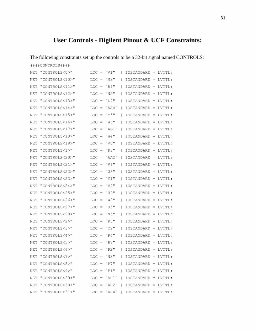
User Controls - Digilent Pinout & UCF Constraints:
The following constraints set up the controls to be a 32-bit signal named CONTROLS:
####CONTROLS####
NET "CONTROLS<0>" LOC = "V1" | IOSTANDARD = LVTTL;
NET "CONTROLS<10>" LOC = "M3" | IOSTANDARD = LVTTL;
NET "CONTROLS<11>" LOC = "R9" | IOSTANDARD = LVTTL;
NET "CONTROLS<12>" LOC = "N2" | IOSTANDARD = LVTTL;
NET "CONTROLS<13>" LOC = "L4" | IOSTANDARD = LVTTL;
NET "CONTROLS<14>" LOC = "AA4" | IOSTANDARD = LVTTL;
NET "CONTROLS<15>" LOC = "Y5" | IOSTANDARD = LVTTL;
NET "CONTROLS<16>" LOC = "W6" | IOSTANDARD = LVTTL;
NET "CONTROLS<17>" LOC = "AB1" | IOSTANDARD = LVTTL;
NET "CONTROLS<18>" LOC = "W4" | IOSTANDARD = LVTTL;
NET "CONTROLS<19>" LOC = "V8" | IOSTANDARD = LVTTL;
NET "CONTROLS<1>" LOC = "R3" | IOSTANDARD = LVTTL;
NET "CONTROLS<20>" LOC = "AA2" | IOSTANDARD = LVTTL;
NET "CONTROLS<21>" LOC = "V6" | IOSTANDARD = LVTTL;
NET "CONTROLS<22>" LOC = "U8" | IOSTANDARD = LVTTL;
NET "CONTROLS<23>" LOC = "Y1" | IOSTANDARD = LVTTL;
NET "CONTROLS<24>" LOC = "V4" | IOSTANDARD = LVTTL;
NET "CONTROLS<25>" LOC = "U9" | IOSTANDARD = LVTTL;
NET "CONTROLS<26>" LOC = "W2" | IOSTANDARD = LVTTL;
NET "CONTROLS<27>" LOC = "U5" | IOSTANDARD = LVTTL;
NET "CONTROLS<28>" LOC = "N5" | IOSTANDARD = LVTTL;
NET "CONTROLS<2>" LOC = "R5" | IOSTANDARD = LVTTL;
NET "CONTROLS<3>" LOC = "T2" | IOSTANDARD = LVTTL;
NET "CONTROLS<4>" LOC = "P4" | IOSTANDARD = LVTTL;
NET "CONTROLS<5>" LOC = "R7" | IOSTANDARD = LVTTL;
NET "CONTROLS<6>" LOC = "P2" | IOSTANDARD = LVTTL;
NET "CONTROLS<7>" LOC = "N3" | IOSTANDARD = LVTTL;
NET "CONTROLS<8>" LOC = "P7" | IOSTANDARD = LVTTL;
NET "CONTROLS<9>" LOC = "P1" | IOSTANDARD = LVTTL;
NET "CONTROLS<29>" LOC = "AH1" | IOSTANDARD = LVTTL;
NET "CONTROLS<30>" LOC = "AH2" | IOSTANDARD = LVTTL;
NET "CONTROLS<31>" LOC = "AH4" | IOSTANDARD = LVTTL;
32
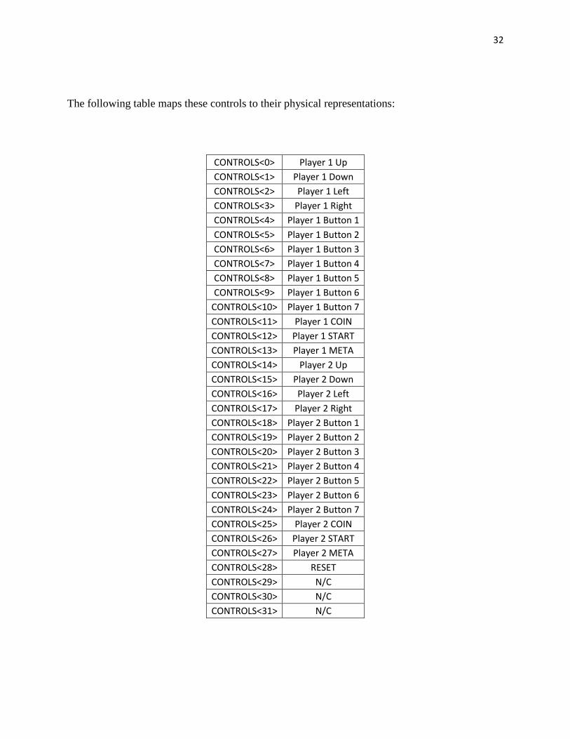
The following table maps these controls to their physical representations:
CONTROLS<0> Player 1 Up
CONTROLS<1> Player 1 Down
CONTROLS<2> Player 1 Left
CONTROLS<3> Player 1 Right
CONTROLS<4> Player 1 Button 1
CONTROLS<5> Player 1 Button 2
CONTROLS<6> Player 1 Button 3
CONTROLS<7> Player 1 Button 4
CONTROLS<8> Player 1 Button 5
CONTROLS<9> Player 1 Button 6
CONTROLS<10> Player 1 Button 7
CONTROLS<11> Player 1 COIN
CONTROLS<12> Player 1 START
CONTROLS<13> Player 1 META
CONTROLS<14> Player 2 Up
CONTROLS<15> Player 2 Down
CONTROLS<16> Player 2 Left
CONTROLS<17> Player 2 Right
CONTROLS<18> Player 2 Button 1
CONTROLS<19> Player 2 Button 2
CONTROLS<20> Player 2 Button 3
CONTROLS<21> Player 2 Button 4
CONTROLS<22> Player 2 Button 5
CONTROLS<23> Player 2 Button 6
CONTROLS<24> Player 2 Button 7
CONTROLS<25> Player 2 COIN
CONTROLS<26> Player 2 START
CONTROLS<27> Player 2 META
CONTROLS<28> RESET
CONTROLS<29> N/C
CONTROLS<30> N/C
CONTROLS<31> N/C
33
Sources
We have included all the documentation in our attached zip file. Below however, are a
list of sites from which these documents, and other information, were retrieved:
http://www.klov.com Game Schematics, Owner’s
Manuals, Theory of
Operation Manuals
http://mamedev.org/ MAME: Code and reference
implementation
http://seanriddle.com/willy.html Reverse Engineering
(Blitter), General Hardware
Overview
http://shop-pdp.kent.edu/ashtml/asxxxx.htm ASXXXX Cross-Assemblers
http://webpages.charter.net/coinopcauldron/piaarticle.html 6821 PIA Theory &
Operation
http://members.optusnet.com.au/jekent/system09/index.html System09: VHDL 6809E
http://www.zimmers.net/anonftp/pub/cbm/documents/chipdata Motorola 6809E
Technical Specifications
http://www.bitsavers.org/pdf/motorola/_dataSheets/ Motorola Datasheets


![VeryLowRateScalableSpeechCodingthroughClassified ...ehsanj/publications/EURASIP_10.pdfEmbedded quantization was first introduced by Tzou [1] for scalar quantization. Tzou proposed](https://static.fdocuments.in/doc/165x107/602a50dcd89ce10f9b6fa2d4/verylowratescalablespeechcodingthroughclassiied-ehsanjpublicationseurasip10pdf.jpg)