Multi-Standard Quad DDC Chip (Rev. B)
99
GC4016 MULTI-STANDARD QUAD DDC CHIP Data Manual PRODUCTION DATA information is current as of publication date. Products conform to specifications per the terms of the Texas Instruments standard warranty. Production processing does not necessarily include testing of all parameters. Literature Number: SLWS133B August 2001 – Revised July 2009
Transcript of Multi-Standard Quad DDC Chip (Rev. B)

GC4016MULTI-STANDARD QUAD DDC CHIP
Data Manual
PRODUCTION DATA information is current as of publication date.Products conform to specifications per the terms of the TexasInstruments standard warranty. Production processing does notnecessarily include testing of all parameters.
Literature Number: SLWS133BAugust 2001–Revised July 2009

Contents
GC4016MULTI-STANDARD QUAD DDC CHIPSLWS133B–AUGUST 2001–REVISED JULY 2009 www.ti.com
1 Introduction......................................................................................................................... 71.1 Features....................................................................................................................... 71.1.1 Block Diagram................................................................................................................ 81.2 Functional Description....................................................................................................... 91.2.1 Control Interface ............................................................................................................. 91.2.2 Input Format ................................................................................................................ 121.2.3 The Downconverters....................................................................................................... 12
1.2.3.1 Zero-Padding..................................................................................................... 141.2.3.2 The Numerically Controlled Oscillator (NCO)................................................................ 161.2.3.3 Five-Stage CIC Filter............................................................................................ 181.2.3.4 Coarse Channel Gain ........................................................................................... 191.2.3.5 The First Decimate-by-Two Filter (CFIR)..................................................................... 191.2.3.6 The Second Decimate-by-Two Filter (PFIR) ................................................................. 201.2.3.7 Complex-to-Real Mode ......................................................................................... 21
1.2.4 Multichannel Modes........................................................................................................ 211.2.4.1 Double-Bandwidth Downconverter Mode (Splitl/Q Mode).................................................. 221.2.4.2 Wideband Downconvert Mode................................................................................. 221.2.4.3 Complex Input, Narrowband Output .......................................................................... 221.2.4.4 Complex-Input, Double-Bandwidth (SplitI/Q) Mode......................................................... 231.2.4.5 Multichannel Summary ......................................................................................... 23
1.2.5 Resampler................................................................................................................... 231.2.5.1 Functional Description .......................................................................................... 241.2.5.2 The Resampler Filter............................................................................................ 251.2.5.3 Restrictions on NMULT ......................................................................................... 261.2.5.4 The Resampler Clock Divider.................................................................................. 271.2.5.5 Final Shift and Round........................................................................................... 271.2.5.6 Bypassing the Resampler ...................................................................................... 271.2.5.7 Adaptive Ratio Change ......................................................................................... 28
1.2.6 Overall Gain................................................................................................................. 281.2.7 Peak Counter ............................................................................................................... 281.2.8 Output Modes............................................................................................................... 29
1.2.8.1 Microprocessor Mode ........................................................................................... 301.2.8.2 Wide-Word Microprocessor Mode............................................................................. 321.2.8.3 Synchronous Serial Outputs ................................................................................... 331.2.8.4 Asynchronous Serial Outputs .................................................................................. 341.2.8.5 Nibble-Mode Output............................................................................................. 361.2.8.6 Link-Mode Output ............................................................................................... 371.2.8.7 Parallel-Mode Output ........................................................................................... 38
1.2.9 Clocking ..................................................................................................................... 391.2.10 Power-Down Modes ...................................................................................................... 401.2.11 Synchronization ........................................................................................................... 401.2.12 Initialization................................................................................................................. 42
1.2.12.1 Initializing Multiple GC4016 Chips ........................................................................... 421.2.12.2 Initializing Stand-Alone GC4016 Chips ..................................................................... 43
1.2.13 Data Latency............................................................................................................... 431.2.14 Diagnostics................................................................................................................. 431.2.15 JTAG........................................................................................................................ 431.2.16 Mask Revision Register .................................................................................................. 43
2 Packaging ......................................................................................................................... 442.1 GC4016PB 160-Ball Plastic Ball-Grid Array (PBGA) .................................................................. 44
Contents2 Submit Documentation Feedback

GC4016MULTI-STANDARD QUAD DDC CHIP
www.ti.com SLWS133B–AUGUST 2001–REVISED JULY 2009
3 Control Registers ............................................................................................................... 493.1 Global Controls ............................................................................................................. 493.2 Paged Registers............................................................................................................ 513.3 CFIR Coefficient Pages ................................................................................................... 513.4 PFIR Coefficient Pages.................................................................................................... 523.5 Channel Frequency Pages................................................................................................ 533.6 Channel Control Pages.................................................................................................... 533.7 Resampler Coefficient Pages (Pages 32–63) .......................................................................... 573.8 Resampler Control Page (Page 64) ..................................................................................... 593.9 Resampler Ratio Page (Page 65)........................................................................................ 613.10 Channel Output Pages (Pages 96 and 97) ............................................................................. 613.11 Output Control Page (Page 98) .......................................................................................... 61
4 Specifications .................................................................................................................... 684.1 Absolute Maximum Ratings............................................................................................... 684.2 Recommended Operating Conditions ................................................................................... 684.3 Thermal Characteristics ................................................................................................... 684.3.1 Power Consumption ....................................................................................................... 684.4 DC Characteristics ......................................................................................................... 694.5 AC Characteristics ......................................................................................................... 70
5 Application Notes ............................................................................................................... 715.1 Power and Ground Connections ......................................................................................... 715.2 Static-Sensitive Device .................................................................................................... 715.3 Moisture-Sensitive Package .............................................................................................. 715.4 Thermal Management ..................................................................................................... 715.5 Example CFIR Filter Sets ................................................................................................. 715.6 Example PFIR Filter Sets ................................................................................................. 725.7 Overall Spectral Responses of Example Filters........................................................................ 745.8 Example Resampler Configurations ..................................................................................... 75
5.8.1 Bypass Mode..................................................................................................... 755.8.2 Resampling Modes.............................................................................................. 75
5.9 GC4016 Configuration Generator ........................................................................................ 765.10 Example GSM Application ................................................................................................ 77
5.10.1 GSM Filter Response ........................................................................................... 775.10.2 Oversampling Using the Resampler .......................................................................... 785.10.3 Gain ............................................................................................................... 785.10.4 GSM Configuration .............................................................................................. 79
5.11 Example IS-136 DAMPS Application .................................................................................... 795.11.1 DAMPS Filter Response........................................................................................ 805.11.2 Oversampling Using the Resampler .......................................................................... 815.11.3 Gain ............................................................................................................... 815.11.4 DAMPS Configuration........................................................................................... 81
5.12 Example IS-95 NB-CDMA Application................................................................................... 835.12.1 IS-95 Filter Response........................................................................................... 835.12.2 Oversampling Using the Resampler .......................................................................... 845.12.3 Gain ............................................................................................................... 845.12.4 IS-95 NB-CDMA Configuration ................................................................................ 84
5.13 UMTS WB-CDMA Applications........................................................................................... 855.13.1 UMTS Filter Response.......................................................................................... 855.13.2 Oversampling Using the Resampler .......................................................................... 865.13.3 Gain ............................................................................................................... 865.13.4 UMTS Configuration ............................................................................................ 87
5.14 Diagnostics.................................................................................................................. 87
Contents 3

GC4016MULTI-STANDARD QUAD DDC CHIPSLWS133B–AUGUST 2001–REVISED JULY 2009 www.ti.com
5.15 Output Test Configuration................................................................................................. 915.16 Revision History ............................................................................................................ 93
REVISION HISTORY ..................................................................................................................... 94
Contents4 Submit Documentation Feedback
GC4016MULTI-STANDARD QUAD DDC CHIP
www.ti.com SLWS133B–AUGUST 2001–REVISED JULY 2009
List of Figures1-1 GC4016 Block Diagram............................................................................................................ 9
1-2 Normal Control I/O Timing ....................................................................................................... 11
1-3 Edge-Write Control Timing....................................................................................................... 12
1-4 Downconverter Channel.......................................................................................................... 16
1-5 Zero-Pad Synchronization ....................................................................................................... 16
1-6 NCO Circuit ........................................................................................................................ 17
1-7 Example NCO Spurs ............................................................................................................. 17
1-8 NCO Peak Spur Plots ............................................................................................................ 18
1-9 Five-Stage CIC Decimate-by-N Filter........................................................................................... 18
1-10 Typical CFIR Specifications ..................................................................................................... 20
1-11 Typical PFIR Specifications...................................................................................................... 21
1-12 Resampler Channel Block Diagram ............................................................................................ 24
1-13 The Resampler Spectral Response ............................................................................................ 26
1-14 Wide-Word Microprocessor Port ................................................................................................ 32
1-15 Serial Output Formats ............................................................................................................ 36
1-16 Parallel-Mode Timing ............................................................................................................. 39
2-1 GC4016 Terminal Assignments ................................................................................................. 45
5-1 cfir_17 With pfir_17 ............................................................................................................... 74
5-2 cfir_34 With pfir_34 ............................................................................................................... 74
5-3 cfir_68 With pfir_68 ............................................................................................................... 74
5-4 cfir_80 With pfir_80 ............................................................................................................... 74
5-5 cfir_100 With pfir_100 ............................................................................................................ 75
5-6 cfir_150 With pfir_150 ............................................................................................................ 75
5-7 Frequency Response for the Example GSM Application .................................................................... 78
5-8 Frequency Response for the Example DAMPS Application................................................................. 80
5-9 Frequency Response for the Example IS-95 Application.................................................................... 83
5-10 Frequency Response for the Example UMTS Application................................................................... 86
List of Figures 5

GC4016MULTI-STANDARD QUAD DDC CHIPSLWS133B–AUGUST 2001–REVISED JULY 2009 www.ti.com
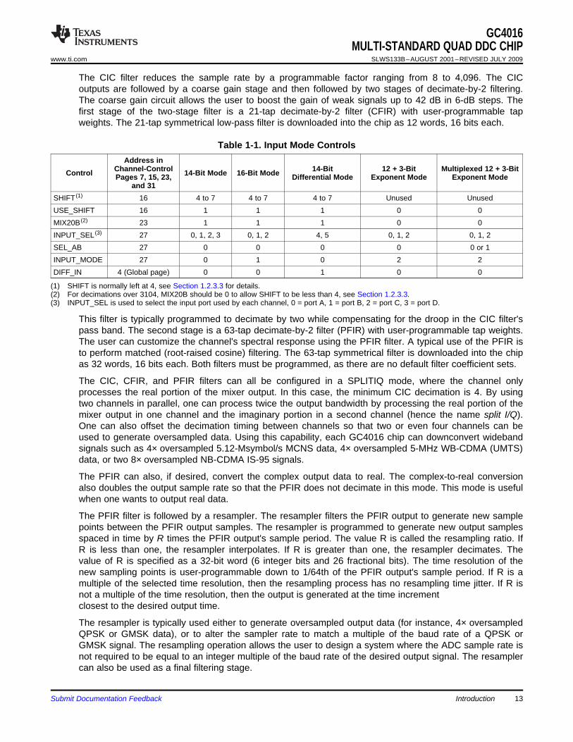
List of Tables1-1 Input Mode Controls .............................................................................................................. 13
1-2 Multichannel Mode Settings ..................................................................................................... 23
1-3 Output Mode Controls ............................................................................................................ 30
1-4 Channel Output Map, Synchronous Four-Channel Mode ................................................................... 31
1-5 Channel Output Map, Synchronous Two-Channel Mode .................................................................... 31
1-6 Channel Output Map, Single-Channel Mode .................................................................................. 32
1-7 Sync Modes........................................................................................................................ 40
1-8 Recommended Sync Settings ................................................................................................... 42
1-9 Mask Revisions.................................................................................................................... 43
2-1 GC4016 Terminal Locations (Top View) ....................................................................................... 46
2-2 Terminal Functions................................................................................................................ 46
3-1 Global Control Registers ......................................................................................................... 49
3-2 Page Assignments ................................................................................................................ 51
3-3 CFIR Coefficient Pages .......................................................................................................... 51
3-4 PFIR Coefficient Pages .......................................................................................................... 52
3-5 Channel Control Registers ....................................................................................................... 53
3-6 Resampler Coefficient Pages (Single-Filter Mode) ........................................................................... 58
3-7 Resampler Control Registers .................................................................................................... 59
3-8 Resampler Ratio Page ........................................................................................................... 61
3-9 Output Control Registers......................................................................................................... 61
5-1 Example CFIR Filters ............................................................................................................. 72
5-2 Default PFIR Filters ............................................................................................................... 73
5-3 Resampler Bypass Mode ........................................................................................................ 75
5-4 Resampler Modes................................................................................................................. 75
5-5 Desired GSM Specifictions ...................................................................................................... 77
5-6 Example GSM Configuration .................................................................................................... 79
5-7 Desired DAMPS Specifications ................................................................................................. 79
5-8 Example DAMPS Configuration ................................................................................................. 81
5-9 Desired IS-95 NB-CDMA Specifications ....................................................................................... 83
5-10 Example IS-95 NB-CDMA Configuration....................................................................................... 84
5-11 Desired UMTS Specifications ................................................................................................... 85
5-12 Example UMTS Configuration................................................................................................... 87
5-13 Diagnostic Test 1, Expected Checksum = EC ................................................................................ 88
5-14 Diagnostic Test 2, Expected Checksum = 4C................................................................................. 88
5-15 Diagnostic Test 3, Expected Checksum = EF................................................................................. 89
5-16 Diagnostic Test 4, Expected Checksum = 18 ................................................................................. 90
5-17 GC4016 Register Assignment Quick Reference Guide ...................................................................... 91
5-18 GC4016 Register Assignment Quick Reference Guide ...................................................................... 92
6 List of Tables Submit Documentation Feedback

1 Introduction
1.1 Features
GC4016MULTI-STANDARD QUAD DDC CHIP
www.ti.com SLWS133B–AUGUST 2001–REVISED JULY 2009
• >115-dB Spurious-Free• Input Rates up to 100 MSPSDynamic Range• Four Independent Digital Downconvert (DDC)
• User Programmable 21-Tap and 63-TapChannelsDecimate-by-Two Filters, Independent per• Single-Channel GC4011 and Dual-ChannelChannelGC4012 Derivatives Are Available
• Nyquist Filtering for QPSK or QAM Symbol• Independent Decimation and ResamplingData• Independent Tuning, Phase and Gain Controls
• Resampler Provides Additional Filtering and• Input Crossbar Switch for: Allows Arbitrary Input/Output Rate Selections– Four 14-Bit Inputs
• Microprocessor Interface for Control– Three 16-Bit Inputs• Built-In Diagnostics– Three 12-Bit + 3-Bit Exponent Inputs• Application Examples:– Two 14-Bit Differential Inputs
– Four 4× Oversampled GSM, DAMPS, or• Decimation Factors of:IS-95 CDMA Carriers– 32 to 16,384 in Each Channel
– Two 8× Oversampled IS-95 CDMA Carriers– 16 to 32 by Combining Two Channels– Two 2× Oversampled 3.84-MB UMTS– 8 to 16 by Combining Four Channels Carriers
• Zero-Padding for Lower Decimation Factors – One 4× Oversampled 3.84-MB UMTS Carrier• Resampler for Arbitrary Decimation Factors • Core Power Consumption at 80 MHz, 2.5 V:• Peak Detection Counters for AGC Loop – 100 mW per DAMPS Channel
Controls – 115 mW per GSM Channel• Outputs Can Be: – 115 mW per IS-95 Channel
– Bit Serial – 620 mW per 3.84-MB UMTS Channel– Nibble Serial (Link Port) • Industrial Temperature Range (–40°C to 85°C)– Parallel Port • GC4016-PB 160-Ball PBGA– Memory-Mapped Registers • Package: 15-mm × 15-mm
• 12-, 16-, 20-, or 24-Bit Output Samples • 3.3-V I/O Voltage, 2.5-V Core Voltage• 0.02-Hz Tuning Resolution • JTAG Boundary Scan• >100-dB Far-Band Rejection
Please be aware that an important notice concerning availability, standard warranty, and use in critical applications of TexasInstruments semiconductor products and disclaimers thereto appears at the end of this document.
PRODUCTION DATA information is current as of publication date. Copyright © 2001–2009, Texas Instruments IncorporatedProducts conform to specifications per the terms of the TexasInstruments standard warranty. Production processing does notnecessarily include testing of all parameters.
1.1.1 Block Diagram
Clo
ck D
oublin
gand
Dis
trib
ution C
ircuit
CK
Contr
ol
Inte
rface
WR
RD
A[0
:4]
C[0
:7]
Sync C
ounte
rand
Dia
gnostic
Test
Genera
tor
SIA
SO
CE
D(B
it S
eria
l O
utp
uts
)
A
(14 B
its)
INB
(14 B
its)
INC
(14 B
its)
IND
(14 B
its)
IN
Cro
ssb
ar
Sw
itch
(16
Bit I
np
ut
an
d 1
2 B
it F
loa
tin
g P
oin
t M
od
es u
se
th
e D
Pin
s f
or
the
LS
Bs o
f In
pu
tsA
, B
, a
nd
C)
INI N
ININ
Outp
ut F
orm
at
Dia
gnostics
24
-Bit P
ara
llel O
utp
ut
SIB
CB
A
Decim
ate
by 4
to 4
KF
ilter
Decim
ate
by 4
to 4
KF
ilter
Decim
ate
by 4
to
4K
Filt
er
De
cim
ate
by 4
to 4
KF
ilter
21
Tap
Pro
gra
mm
able
Decim
ate
by 2
Filt
er
(CF
IR)
21
Tap
Pro
gra
mm
able
Decim
ate
by 2
Filt
er
(CF
IR)
21
Tap
Pro
gra
mm
able
Decim
ate
by 2
Filt
er
(CF
IR)
21
Tap
Pro
gra
mm
able
Decim
ate
by 2
Filt
er
(CF
IR)
63
Tap
Pro
gra
mm
able
Decim
ate
by 2
Filt
er
(PF
IR)
63
Tap
Pro
gra
mm
able
Decim
ate
by 2
Filt
er
(PF
IR)
63
Tap
Pro
gra
mm
able
Decim
ate
by 2
Filt
er
(PF
IR)
63
Tap
Pro
gra
mm
able
Decim
ate
by 2
Filt
er
(PF
IR)
Com
bin
es C
hannels
, F
ilters
, R
esam
ple
sA
nd
Adju
sts
Gain
(Filt
ering, R
esam
plin
g a
nd G
ain
Adju
stm
ents
are
Perf
orm
ed Indep
en
dently O
n E
ach C
ha
nn
el)
JTA
G
Boundary
Scan
Test
Logic
TC
KT
MS
TD
IT
DO
Acknow
ledge
(Lin
k M
ode)
NCOSine/CosineGenerator
NCOSine/CosineGenerator
NCOSine/CosineGenerator
NCOSine/CosineGenerator Tuning
Frequency
TuningFrequency
TuningFrequency
TuningFrequency
PhaseOffset
PhaseOffset
PhaseOffset
PhaseOffset
Bit-Clock
Frame Syncs
Ready
B0
18
7-0
1
GC4016MULTI-STANDARD QUAD DDC CHIPSLWS133B–AUGUST 2001–REVISED JULY 2009 www.ti.com
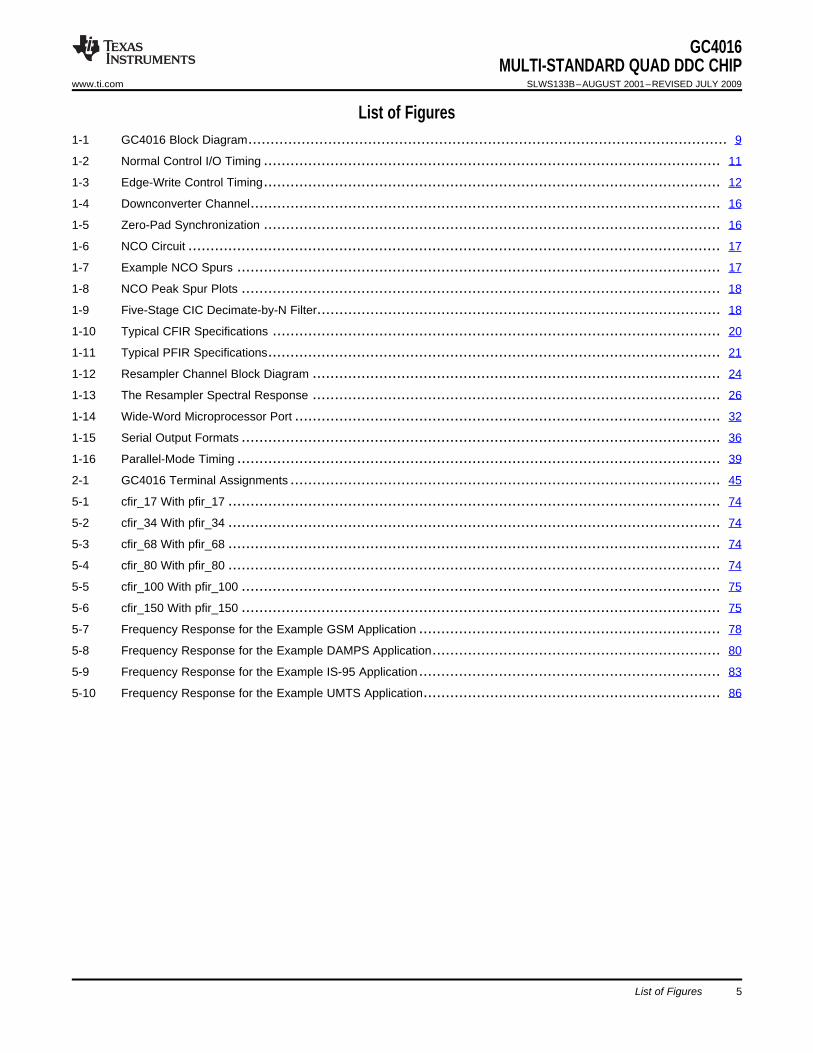
Figure 1-1. GC4016 Block Diagram
Introduction8 Submit Documentation Feedback

1.2 Functional Description
1.2.1 Control Interface
GC4016MULTI-STANDARD QUAD DDC CHIP
www.ti.com SLWS133B–AUGUST 2001–REVISED JULY 2009
The GC4016 quad receiver chip contains four identical downconversion circuits. Each downconversioncircuit accepts a real sample rate up to 100 MHz, downconverts a selected carrier frequency to zero,decimates the signal rate by a programmable factor ranging from 32 to 16,384, and then resamples thechannel to adjust the sample rate up or down by an arbitrary factor. In the real output mode, the outputsample rate is doubled and the signal is output as a real signal centered at fout/4. The channels may becombined to produce wider band and/or oversampled outputs or to process complex input data. The chipoutputs the downconverted signals in any one of several formats (microprocessor, four serial lines, oneTDM serial line, nibble, link, or 24-bit parallel port. The chip contains two user-programmable output filtersper path which can be used to shape arbitrarily the received data spectrum. These filters can be used asNyquist receive filters for digital data transmission. The chip also contains a resampling filter to provideadditional filtering and to allow the user complete flexibility in the selection of input and output samplerates.
Two downconverter paths can be merged to be used as a single complex input downconversion circuit.Two paths may also be combined to support wider band output rates or oversampled outputs. Four pathsmay be combined to support both wider band output and oversampling.
The downconverters are designed to maintain over 115 dB of spurious-freedynamic range and over 100 dB of out-of-band rejection. A five-stage CIC and 20-bit internal data pathssupport this high-dynamic-range signal-processing requirement. Each downconvert circuit accepts 16-bitinputs and produces 24-bit outputs (can be rounded back to 12, 16, or 20 bits). The frequencies andphase offsets of the four sine/cosine sequence generators can be independently specified, as can thedecimation and filter parameters of each circuit.
On-chip diagnostic circuits are provided to simplify system debug and maintenance.
The chip receives configuration and control information over a microprocessor-compatible bus consistingof an 8-bit data I/O port, a 5-bit address port, a chip-enable strobe, a read strobe, and a write strobe. Thechip's control registers (8 bits each) are memory mapped into the 5-bit address space of the control port.
The applications section,Section 5. illustrates how to set the control registers and coefficients for specificwireless-communication standards.
The chip is configured by writing control information into control registers within the chip. The controlregisters are grouped into eight global registers and 128 pages of registers, each page containing up to 16registers. The global registers are accessed as addresses 0 through 7. Address 2 is the page register thatselects which page is accessed by addresses 16 through 31. The contents of these control registers andhow to use them are described in Section 3.
The registers are written to or read from using the C[0:7], A[0:4], CE, RD, and WR terminals. Eachcontrol register has been assigned a unique address within the chip. This interface is designed to allowthe GC4016 chip to appear to an external processor as a memory-mapped peripheral (the RD terminal isequivalent to a memory-chip OE terminal).
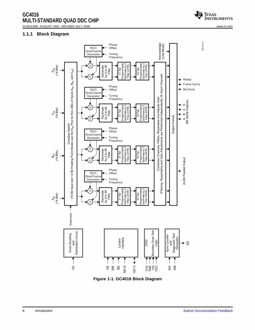
An external processor (a microprocessor, computer, or DSP chip) can write into a register by settingA[0:4] to the desired register address, selecting the chip using the CE terminal, setting C[0:7] to thedesired value, and then pulsing WR low. The data is written into the selected register when both WR andCE are low, and is held when either signal goes high. An alternate edge-write mode can be used to strobethe data into the selected register when either WR or CE goes high. This is useful for processors that donot specifyvalid data when the write strobe goes low, but specify that the data must be stable before the write strobegoes high. The edge-write mode is necessary for these processors, as some control registers (such asmost sync or reset registers) are sensitive to transient values on the C[0:7] data bus.
Submit Documentation Feedback Introduction 9
GC4016MULTI-STANDARD QUAD DDC CHIPSLWS133B–AUGUST 2001–REVISED JULY 2009 www.ti.com
To read from a control register, the processor must set A[0:4] to the desired address, select the chip withthe CE terminal, and then set RD low. The chip then drives C[0:7] with the contents of the selectedregister. After the processor has read the value from C[0:7], it should set RD and CE high. The C[0:7]terminals are turned off (high impedance) whenever CE or RD is high or when WR is low. The chip onlydrives these terminals when both CE and RD are low and WR is high.
One can also ground the RD terminal and use the WR terminal as a read/write direction control and usethe CE terminal as a control I/O strobe. Figure 1-2 shows timing diagrams illustrating both I/O modes.
The edge-write mode, enabled by the EDGE_WRITE control bit in register 0, allows for rising-edge writecycles. In this mode, the C[0:7] data only must be stable for a setup time before the rising edge of thewrite strobe, and held for a small hold time afterward. This mode is appropriate for processors that do notprovide stable data before the start of the write pulse. Figure 1-3 shows the timing for this mode.
The setup, hold, and pulse-duration requirements for control read or write operations are given inSection 4.
The chip also operates in a 4-bit address mode, which is intended to be used with the expansion bus ofthe 4-address-bit TI320C6X DSP chip. Address terminal A3 is grounded in this mode, and the LSB of thepage register (address 2) is used in its place. The 4-bit mode is turned on using the 4_BIT_ADDRESScontrol bit in address 4.
10 Introduction Submit Documentation Feedback

tCSU
tCSPW
tREC
tREC
tREC
tREC
tREC
tCSU
tCSPW
tREC
tCDLY
tCDLY
CE
CE
CE
tREC
tCSU
tCSU
tCSU
Read Cycle - Normal Mode
Read Cycle - Held LOWRD
Write Cycle - Held LOWRD
tCZ
tCZ
tCHDtCHD
WR
WR
WR
RD
C[0–7]
C[0–7]
C[0–7]
A[0–4]
A[0–4]
A[0–4]
CE
tREC
tCSU
Write Cycle - Normal Mode
tCHD
WR
RD
C[0–7]
A[0–4]
T0169-01
GC4016MULTI-STANDARD QUAD DDC CHIP
www.ti.com SLWS133B–AUGUST 2001–REVISED JULY 2009
Figure 1-2. Normal Control I/O Timing
Submit Documentation Feedback Introduction 11
tCSU
tCSPW
tREC
CE
tREC
tEWCSU
tCSU
Edge Write Mode
tCHD
WR
RD
C[0–7]
A[0–4]
T0170-01
1.2.2 Input Format
1.2.3 The Downconverters
GC4016MULTI-STANDARD QUAD DDC CHIPSLWS133B–AUGUST 2001–REVISED JULY 2009 www.ti.com
Figure 1-3. Edge-Write Control Timing
The chip accepts five input formats:• Four input ports of 14-bit data• Three input ports of 16-bit data• Two input ports of 14-bit, low-voltage differential data• Three ports of 12-bit floating-point data with 3-bit exponent• Three ports of multiplexed, dual-channel, 12-bit floating-point data with 3-bit exponent
The 12-, 14-, and 16-bit input words are in a 2s-complement format. The MSB_POL control bit inaddress 27 of the channel-control pages can be used to convert offset binary data to the desired2s-complement format. The 3-bit exponent in the floating-point format is an unsigned integer ranging from0 to 7. All inputs are converted to the internal 19-bit format at the input to each channel. The 14- and16-bit input words are put into the upper 14 and 16 bits, respectively, of the 19-bit word. The unused LSBsare cleared.
The 12-bit floating-point word is shifted down, sign-extended by the amount specified by the 3-bitexponent, and then put into the MSBs of 19-bit word.
A crossbar switch allows the user to route any input source to any downconverter channel.
Table 1-1 shows the suggested control register settings required for each input mode. See Section 3.6 fordetailed descriptions of each control setting.
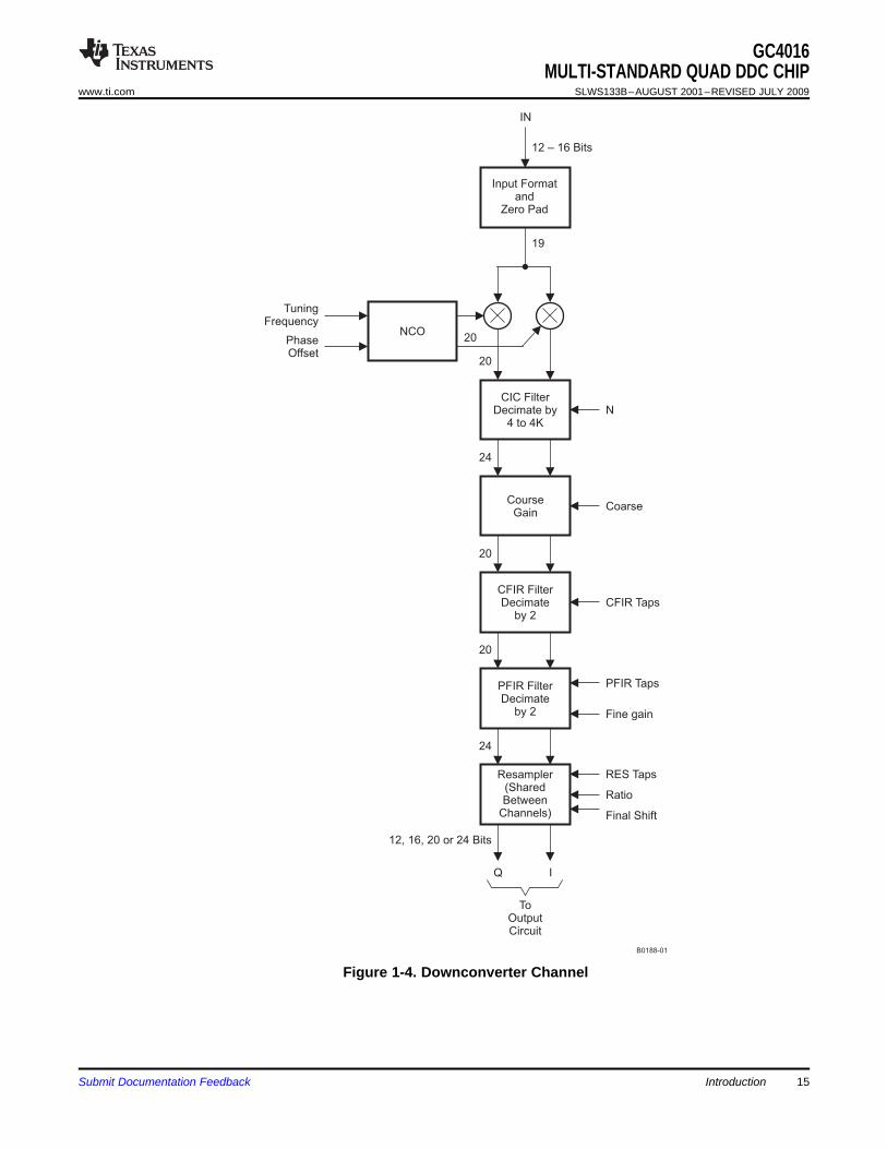
Each downconverter contains an NCO and a mixer to quadrature downconvert the signal to baseband,followed by a five-stage cascade-integrate comb (CIC) filter (1) and two stages of decimate-by-two filteringto isolate the desired signal. The signal is then sent to a resampler, which can increase or decrease thefinal output sample rate to match the post-processing requirements for baud-rate sampling oroversampling.
A block diagram of the channel is shown in Figure 1-4.
The INPUT FORMAT circuit converts the selected input data into the 19-bit format described inSection 1.2.2. The zero-pad function allows the user to clock the chip at a higher rate than the inputsample rate.
The NCO/mixer circuit tunes the desired center frequency down to dc, where it is low-pass filtered by theCIC, CFIR, PFIR, and resampler filters.
(1) Hogenhauer, An Economical Class of Digital Filters for Decimation and Interpolation, IEEE transactions on ASSP, April 1981.
Introduction12 Submit Documentation Feedback
GC4016MULTI-STANDARD QUAD DDC CHIP
www.ti.com SLWS133B–AUGUST 2001–REVISED JULY 2009
The CIC filter reduces the sample rate by a programmable factor ranging from 8 to 4,096. The CICoutputs are followed by a coarse gain stage and then followed by two stages of decimate-by-2 filtering.The coarse gain circuit allows the user to boost the gain of weak signals up to 42 dB in 6-dB steps. Thefirst stage of the two-stage filter is a 21-tap decimate-by-2 filter (CFIR) with user-programmable tapweights. The 21-tap symmetrical low-pass filter is downloaded into the chip as 12 words, 16 bits each.
Table 1-1. Input Mode ControlsAddress in
Channel-Control 14-Bit 12 + 3-Bit Multiplexed 12 + 3-BitControl 14-Bit Mode 16-Bit ModePages 7, 15, 23, Differential Mode Exponent Mode Exponent Modeand 31
SHIFT (1) 16 4 to 7 4 to 7 4 to 7 Unused UnusedUSE_SHIFT 16 1 1 1 0 0MIX20B (2) 23 1 1 1 0 0INPUT_SEL (3) 27 0, 1, 2, 3 0, 1, 2 4, 5 0, 1, 2 0, 1, 2SEL_AB 27 0 0 0 0 0 or 1INPUT_MODE 27 0 1 0 2 2DIFF_IN 4 (Global page) 0 0 1 0 0
(1) SHIFT is normally left at 4, see Section 1.2.3.3 for details.(2) For decimations over 3104, MIX20B should be 0 to allow SHIFT to be less than 4, see Section 1.2.3.3.(3) INPUT_SEL is used to select the input port used by each channel, 0 = port A, 1 = port B, 2 = port C, 3 = port D.
This filter is typically programmed to decimate by two while compensating for the droop in the CIC filter'spass band. The second stage is a 63-tap decimate-by-2 filter (PFIR) with user-programmable tap weights.The user can customize the channel's spectral response using the PFIR filter. A typical use of the PFIR isto perform matched (root-raised cosine) filtering. The 63-tap symmetrical filter is downloaded into the chipas 32 words, 16 bits each. Both filters must be programmed, as there are no default filter coefficient sets.
The CIC, CFIR, and PFIR filters can all be configured in a SPLITIQ mode, where the channel onlyprocesses the real portion of the mixer output. In this case, the minimum CIC decimation is 4. By usingtwo channels in parallel, one can process twice the output bandwidth by processing the real portion of themixer output in one channel and the imaginary portion in a second channel (hence the name split I/Q).One can also offset the decimation timing between channels so that two or even four channels can beused to generate oversampled data. Using this capability, each GC4016 chip can downconvert widebandsignals such as 4× oversampled 5.12-Msymbol/s MCNS data, 4× oversampled 5-MHz WB-CDMA (UMTS)data, or two 8× oversampled NB-CDMA IS-95 signals.
The PFIR can also, if desired, convert the complex output data to real. The complex-to-real conversionalso doubles the output sample rate so that the PFIR does not decimate in this mode. This mode is usefulwhen one wants to output real data.
The PFIR filter is followed by a resampler. The resampler filters the PFIR output to generate new samplepoints between the PFIR output samples. The resampler is programmed to generate new output samplesspaced in time by R times the PFIR output's sample period. The value R is called the resampling ratio. IfR is less than one, the resampler interpolates. If R is greater than one, the resampler decimates. Thevalue of R is specified as a 32-bit word (6 integer bits and 26 fractional bits). The time resolution of thenew sampling points is user-programmable down to 1/64th of the PFIR output's sample period. If R is amultiple of the selected time resolution, then the resampling process has no resampling time jitter. If R isnot a multiple of the time resolution, then the output is generated at the time incrementclosest to the desired output time.
The resampler is typically used either to generate oversampled output data (for instance, 4× oversampledQPSK or GMSK data), or to alter the sampler rate to match a multiple of the baud rate of a QPSK orGMSK signal. The resampling operation allows the user to design a system where the ADC sample rate isnot required to be equal to an integer multiple of the baud rate of the desired output signal. The resamplercan also be used as a final filtering stage.
Submit Documentation Feedback Introduction 13

1.2.3.1 Zero-Padding
GC4016MULTI-STANDARD QUAD DDC CHIPSLWS133B–AUGUST 2001–REVISED JULY 2009 www.ti.com
A final shift circuit allows the user to shift the data by up to 15 bits to place it properly in the output word.The output word may be rounded to 12,16, 20, or 24 bits.
The data may be output from the chip via a microprocessor interface, serial terminals, or using a parallelport. The parallel port is particularly valuable for wideband output data.
The input samples are normally clocked into the chip at the clock rate, i.e., the input sample rate is equalto the clock rate. Input rates lower than the clock rate can be accepted by using the zero-pad mode. Whenenabled by setting the ZPAD_EN bit in address 19 of the channel control pages, the zero-pad modeinserts NZERO zeroes between each input sample, where NZERO ranges from 0 to 15, allowing inputdata rates down to 1/16th the clock rate. NZERO is set in address 19.
14 Introduction Submit Documentation Feedback
Input Formatand
Zero Pad
CIC FilterDecimate by
4 to 4K
CFIR FilterDecimate
by 2
PFIR FilterDecimate
by 2
Resampler(SharedBetween
Channels)
CourseGain
IN
12 – 16 Bits
19
NCO
TuningFrequency
PhaseOffset
N
CFIR Taps
Ratio
PFIR Taps
RES Taps
Fine gain
Final Shift
Coarse
20
20
24
24
20
20
Q I
ToOutputCircuit
12, 16, 20 or 24 Bits
B0188-01
GC4016MULTI-STANDARD QUAD DDC CHIP
www.ti.com SLWS133B–AUGUST 2001–REVISED JULY 2009
Figure 1-4. Downconverter Channel
Submit Documentation Feedback Introduction 15

CK
SIB
Input
Sample Taken
Data is Sampled Every(NZERO + 1) Clocks Thereafter
• • •
3 + NZERO Clocks
T0171-01
1.2.3.2 The Numerically Controlled Oscillator (NCO)
GC4016MULTI-STANDARD QUAD DDC CHIPSLWS133B–AUGUST 2001–REVISED JULY 2009 www.ti.com
Figure 1-5. Zero-Pad Synchronization
Zero-padding lowers the effective decimation ratio. For example, the minimum complex output decimationusing a single channel is normally 32. If the input data rate is 5 MSPS and the system can clock the chipat 40 MHz, then the zero-pad function can be used to insert seven zeros between each sample, paddingthe 5-MSPS input data rate up by a factor of eight to 40 MSPS. The minimum decimation of 32 from the40-MHz rate results in an output rate of 1.25 MSPS, which is an effective decimation of 4 relative to theoriginal 5-MSPS data.
A sync signal is used to synchronize the zero-padding. The ZPAD_SYNC control in address 19 selects thesource of the sync signal. The sync signal can be used to identify when the chip samples the input data.Figure 1-5 shows the timing when SIB (ZPAD_SYNC = 3) is selected as the sync source.
Zero-padding can be used to synchronize extracting data from a TDM bus. By adjusting the timing of SIBas shown in Figure 1-5, the user can choose which sample to take from the TDM bus.
The zero-pad function has a gain equal to:ZPAD_GAIN = 1/(1 + NZERO).
The tuning frequency of each downconverter is specified as a 32-bit word, and the phase offset isspecified as a 16-bit word. The NCOs can be synchronized with NCOs on other chips. This allows multipledownconverter outputs to be coherently combined, each with a unique phase and amplitude. A blockdiagram of the NCO circuit is shown in Figure 1-6.
The tuning frequency is set to FREQ according to the formula FREQ = 232f/fCK, where f is the desiredtuning frequency and fCK is the chip clock rate. The 16-bit phase-offset setting is PHASE = 216P/2π, whereP is the desired phase in radians ranging between 0 and 2π.
Note that a positive tuning frequency should be used to downconvert the signal. A negative tuningfrequency can be used to upconvert the negative (spectrally flipped) image of the desired signal. FREQand PHASE are set in addresses 16 through 21 of each channel-frequency page.
The NCO frequency, phase, and accumulator can be initialized and synchronized with other channelsusing the FREQ_SYNC, PHASE_SYNC, and NCO_SYNC controls in addresses 17 and 18 of the channelcontrol pages. The FREQ_SYNC and PHASE_SYNC controls determine when new frequency and phasesettings become active. Normally, these are set to always so that they take effect immediately, but can beused to synchronize frequency-hopping or beam-forming systems. The NCO_SYNC control is usually setto never, but can be used to synchronize the LOs of multiple channels.
The NCO spur level is reduced to below –113 dB through the use of phase dithering. The spectra inFigure 1-7 show the NCO spurs for a worst-case tuning frequency before and after dithering has beenturned on. Notice that the spur level decreases from –105 dB to –116 dB. Dithering is turned on or offusing the DITHER_SYNC control in address 18.
Introduction16 Submit Documentation Feedback

B0189-01
Frequency 32 Bits
32 Bits
16 Bits 5 Bits
Phase
23 MSBs 20 Bits18 MSBs Sin/CosLookupTable
DitherGenerator
Sin/Cos Out
−150
−100
−50
0
0.0 0.1 0.2 0.3 0.4 0.5 0.6 0.7 0.8 0.9 1.0
f − Frequency − f S
Gai
n −
dB
G001
FREQ = 5/24 fS
–105 dB
−150
−100
−50
0
0.0 0.1 0.2 0.3 0.4 0.5 0.6 0.7 0.8 0.9 1.0
f − Frequency − f S
Gai
n −
dB
G002
FREQ = 5/24 fS
–116 dB
GC4016MULTI-STANDARD QUAD DDC CHIP
www.ti.com SLWS133B–AUGUST 2001–REVISED JULY 2009
The worst-case NCO spurs at –113 dB dB to –116 dB, such as the one shown in Figure 1-7(b), are due toa few frequencies that are related to the sampling frequency by multiples of fCK/96 and fCK/124. In thesecases, the rounding errors in the sine/cosine lookup table repeat in a regular fashion, therebyconcentrating the error power into a single frequency rather than spreading it across the spectrum. Theseworst-case spurs can be eliminated by selecting an initial phase that minimizes the errors or by changingthe tuning frequency by a small amount (50 Hz). Setting the initial phase to 4 for multiples of fCK/96 orfCK/124 (and to 0 for other frequencies) results in spurs below –115 dB for all frequencies.
Figure 1-6. NCO Circuit
a) Worst-Case Spectrum Without Dither b) Spectrum With Dither (Tuned to Same Frequency)
Figure 1-7. Example NCO Spurs
Submit Documentation Feedback Introduction 17

−150
−100
−50
0
0.0 0.1 0.2 0.3 0.4 0.5 0.6 0.7 0.8 0.9 1.0
f − Frequency − kHz
Gai
n −
dB
G003
–107 dB
−150
−100
−50
0
0.0 0.1 0.2 0.3 0.4 0.5 0.6 0.7 0.8 0.9 1.0
f − Frequency − kHz
Gai
n −
dB
G004
–121 dB
1.2.3.3 Five-Stage CIC Filter
Data In Data Out
CIC
_S
CA
LE
De
cim
ate
by F
acto
ro
f N20 Bits 24 Bits
Upper24 Bits
Clocked at Full Rate Clocked at 1/N Rate
B0190-01
GC4016MULTI-STANDARD QUAD DDC CHIPSLWS133B–AUGUST 2001–REVISED JULY 2009 www.ti.com
Plot Without Dither or Phase Initialization Plot With Dither and Phase Initialization
Figure 1-8. NCO Peak Spur Plots
Figure 1-8 shows the maximum spur levels as the tuning frequency is scanned over a portion of thefrequency range with the peak-hold function of the spectrum analyzer turned on. Notice that the peak spurlevel is –107 dB before dithering and is –121 dB after dithering has been turned on and the phaseinitialization described previously has been used.
The output of the mixer may be rounded to 16 or 20 bits. Twenty-bit rounding (MIX20B is set in address23) is normally used with the 14- or 16-bit input modes. Sixteen-bit rounding (MIX20B disabled) isnormally used with the floating-point, 12-bit input modes. Sixteen-bit rounding is also required to achieve aCIC gain of less than or equal to unity when the CIC decimation is greater than 3,104. See Table 1-1.
The mixer outputs are decimated by a factor of N in a five-stage CIC filter, where N is any integer between8 and 4096 (between 4 and 2048 for SPLITIQ mode). The value of N is programmed independently foreach channel in addresses 21 and 22 of each channel control page. The programmable decimation allowsthe chip's usable output bandwidth to range from less than 4 kHz to over 3 MHz when the input rate is100 MHz. Wider output bandwidths are obtainable by using multiple channels (see Section 1.2.4). A blockdiagram of the CIC filter is shown in Figure 1-9.
Figure 1-9. Five-Stage CIC Decimate-by-N Filter
The CIC filter has a gain equal to N5 which must be compensated for in the CIC_SCALE circuit shown inFigure 1-9. The CIC_SCALE circuit has a gain equal to 2(SHIFT + SCALE + 6 × BIG_SCALE – 62), where SCALEranges from 0 to 5 and BIG_SCALE ranges from 0 to 7. The range of SHIFT is 4–7 if MIX20B is enabledand is 0–7 if MIX20B is disabled. The overall gain of the CIC circuit is equal to:
CIC_GAIN = N5 × 2(SHIFT + SCALE + 6 × BIG_SCALE – 62)
Introduction18 Submit Documentation Feedback

1.2.3.4 Coarse Channel Gain
1.2.3.5 The First Decimate-by-Two Filter (CFIR)
GC4016MULTI-STANDARD QUAD DDC CHIP
www.ti.com SLWS133B–AUGUST 2001–REVISED JULY 2009
The user must select values for SHIFT, SCALE and BIG_SCALE (addresses 16 and 23 of each channelcontrol page) such that CIC_GAIN (including ZPAD_GAIN if blanking is used) is less than one, i.e.,SHIFT, SCALE, and BIG_SCALE must be selected such that:
(SHIFT + SCALE + 6 × BIG_SCALE) ≤ (62 – 5log2N + log2(NZERO+1) )
Overflows due to improper gain settings go undetected if this relationship is violated. For example, if N isequal to 8 and SHIFT = 4, then this restriction means that BIG_SCALE and SCALE should be less than orequal to 7 and 1, respectively. The SHIFT, BIG_SCALE, and SCALE settings are independent for eachchannel. See Section 1.2.7 for a description of the overall channel gain.
The gain of each channel can be boosted up to 42 dB by shifting the output of the CIC filter up by 0 to 7bits prior to rounding it to 20 bits. The coarse gain is: COARSE_GAIN = 2COARSE, where COARSE rangesfrom 0 to 7. COARSE is set in address 25 of each channel control page. Overflows in the coarse gaincircuit are saturated to plus or minus full scale. The coarse gain is used to increase the gain of anindividual signal after the input bandwidth of the downconverter has been reduced by a factor of N in theCIC filter. If the signal power across the input bandwidth is relatively flat, as is the case in most frequencydivision multiplexed (FDM) systems, then one would want to boost the signal power out of the CIC filter bya factor of COARSE_GAIN = √N. Each channel can be given its own coarse gain setting. SeeSection 1.2.6for a description of the channel's overall gain.
The CIC/coarse gain outputs are filtered by two stages of filtering. The first stage is a 21-tapdecimate-by-two filter with programmable 16-bit coefficients. Because this filter decimates by two, a stopband must be created in that portion of the spectrum that would alias into the signal of interest. This filterhas very lax transition-band specifications, so 21 taps are sufficient both to provide the requiredanti-aliasing stop band and to provide compensation for the droop in the CIC-filter pass band. The CFIR isalso used, in some cases, to provide additional stop-band rejection for the second-stage PFIR filter.Figure 1-10 illustrates the pass-band and stop-band requirements of the filter. fCFIR is the input sample rateto the CFIR filter. fCFIR/4 is the output sample rate of the channel before resampling.
The user-downloaded filter coefficients are 16-bit 2s-complement numbers. Unity gain is achieved throughthe filter if the sum of the 21 coefficients is equal to 65,536. If the sum is not 65,536, then CFIR introducesa gain equal to CFIR_GAIN = CFIR_SUM/65,536, where CFIR_SUM is the sum of the 21 coefficients.Coefficient sets for a variety of standards in cellular and cable modem applications are given in Section 5.The output of CFIR is rounded to 20 bits (using the round-to-even algorithm). Overflows are detected andhard-limited. Overflows can be directed to the channel-overflow detection block.
The 21 coefficients are identified as coefficients h0 through h20, where h10 is the center tap. Thecoefficients are assumed to be symmetric, so only the first 11 coefficients (h0 through h10) are loaded intothe chip. A non-symmetric mode (NO_SYM_CFIR in address 25) allows the user to download an 11-tapnon-symmetric filter as taps h0 through h10. The newest sample is multiplied by h0 and the oldest ismultiplied by h10. NOTE: Filters normally multiply h0 by the oldest data; hence, one may wish to reversethe tap order in the non-symmetric mode.
CFIR has a programmable delay of one CFIR input sample. This delay is used in a multichannel mode toalter the decimate-by-two phasing in order to generate oversampled or wider-bandwidth output data. Thisdelay is independently programmable for each channel and is also independent for I and Q (QDLY_CFIRand IDLY_CFIR in address 25). A special mode (SPLITIQ in address 24) is also available where CFIRgenerates two I outputs rather than one I and one Q. See Section 1.2.4 for details.
Submit Documentation Feedback Introduction 19

Frequency0
–100 dB
0 dB
Signal of Interest Passband (Typically 0.05 to 0.125 f )CFIR
f /8CFIR f /4CFIR f /2CFIR
Stopband (Typically Starts at 0.375 f )CFIR
Very Wide Transition BandP
ow
er
M0061-01
1.2.3.6 The Second Decimate-by-Two Filter (PFIR)
GC4016MULTI-STANDARD QUAD DDC CHIPSLWS133B–AUGUST 2001–REVISED JULY 2009 www.ti.com
Figure 1-10. Typical CFIR Specifications
The second-stage decimate-by-two filter is a 63-tap decimate-by-two filter with programmable 16-bitcoefficients. Fine gain is applied at the output of the PFIR and rounded to 24 bits. Overflows are detectedand hard-limited. Overflows can be directed to the channel overflow detection block.
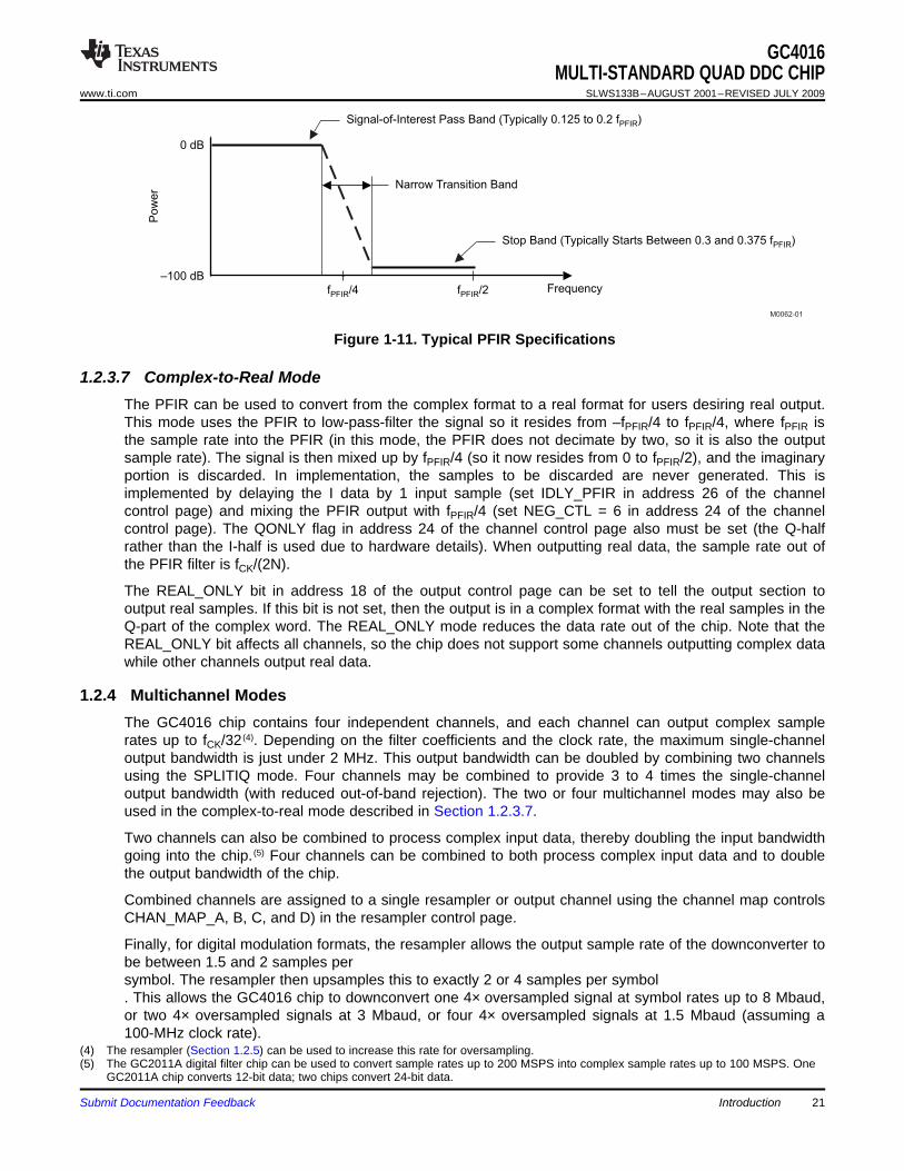
PFIR coefficient sets for a variety of standards in cellular and cable modem applications are given inSection 5. The PFIR-filter pass band must be flat in the region of the signal of interest, and have thedesired out-of-band rejection in the region that aliases into the signal bandwidth after decimation.Figure 1-11 illustrates the pass-band and stop-band requirements of the filter. fPFIR is the input sample rateto the PFIR filter. fPFIR/2 is the output sample rate of the channel before resampling.
The externally downloaded coefficients can be used to tailor the spectral response to the user's needs.For example, it can be programmed as a Nyquist (typically a root-raised-cosine) filter for matched filteringof digital data. The user-downloaded filter coefficients are 16-bit 2s-complement numbers. Unity gain isachieved through the filter if the sum of the 63 coefficients is equal to 65,536. If the sum is not 65,536,then the PFIR introduces a gain equal to PFIR_GAIN = PFIR_SUM/65,536, where PFIR_SUM is the sumof the 63 coefficients.
The 63 coefficients are identified as coefficients h0 through h62, where h31 is the center tap. Thecoefficients are assumed to be symmetric, so only the first 32 coefficients (h0 through h31) are loaded intothe chip. A non-symmetric mode (NO_SYM_PFIR in address 26) allows the user to download a 32-tapnon-symmetric filter as taps h0 through h31. The newest sample is multiplied by h0 and the oldest ismultiplied by h31. NOTE: Filters normally multiply h0 by the oldest data; hence, one may wish to reversethe tap order in the non-symmetric mode.
The output samples can be multiplied by ±1 using a 4-bit control (NEG_CTL in register 24). If the LSB ofNEG_CTL is a 1, the even-time real words are multiplied by –1. The second LSB controls the even-timeimaginary words. The third controls the odd-time real, and the fourth the odd-time imaginary. These canbe used to invert the signal (NEG_CTL = 0xF), frequency shift by fS/2 (NEG_CTL = 0x3), or flip thespectrum (NEG_CTL = 0xA). The NEG_CTL frequency shift can beused for complex-to-real conversion (see Section 1.2.3.7).
A fine gain is applied to the data after filtering and negation. The fine gain is a positive 14-bit integer(FINE) ranging from 0 to 16,383. Fine gain is equal to FINE_GAIN = FINE/1,024. Setting FINE to zeroclears the channel. The GAIN_SYNC control in address 22 can be used to determine when a new finegain setting takes effect. It is normally set to take effect immediately, but can be used to synchronize thegain changes between multiple channels in a beam-forming system.
The PFIR also contains a one-PFIR sample input delay that is independently programmable for the I andQ paths and for the four channels (QDLY_PFIR and IDLY_PFIR in address 26). The delay is used whencombining channels to allow wider output bandwidth and/or more oversampling. It is also used forcomplex-to-real conversion in the PFIR.
Introduction20 Submit Documentation Feedback
Frequency–100 dB
0 dB
Signal-of-Interest Pass Band (Typically 0.125 to 0.2 f )PFIR
f /4PFIR f /2PFIR
Stop Band (Typically Starts Between 0.3 and 0.375 f )PFIR
Narrow Transition Band
Po
we
r
M0062-01
1.2.3.7 Complex-to-Real Mode
1.2.4 Multichannel Modes
GC4016MULTI-STANDARD QUAD DDC CHIP
www.ti.com SLWS133B–AUGUST 2001–REVISED JULY 2009
Figure 1-11. Typical PFIR Specifications
The PFIR can be used to convert from the complex format to a real format for users desiring real output.This mode uses the PFIR to low-pass-filter the signal so it resides from –fPFIR/4 to fPFIR/4, where fPFIR isthe sample rate into the PFIR (in this mode, the PFIR does not decimate by two, so it is also the outputsample rate). The signal is then mixed up by fPFIR/4 (so it now resides from 0 to fPFIR/2), and the imaginaryportion is discarded. In implementation, the samples to be discarded are never generated. This isimplemented by delaying the I data by 1 input sample (set IDLY_PFIR in address 26 of the channelcontrol page) and mixing the PFIR output with fPFIR/4 (set NEG_CTL = 6 in address 24 of the channelcontrol page). The QONLY flag in address 24 of the channel control page also must be set (the Q-halfrather than the I-half is used due to hardware details). When outputting real data, the sample rate out ofthe PFIR filter is fCK/(2N).
The REAL_ONLY bit in address 18 of the output control page can be set to tell the output section tooutput real samples. If this bit is not set, then the output is in a complex format with the real samples in theQ-part of the complex word. The REAL_ONLY mode reduces the data rate out of the chip. Note that theREAL_ONLY bit affects all channels, so the chip does not support some channels outputting complex datawhile other channels output real data.
The GC4016 chip contains four independent channels, and each channel can output complex samplerates up to fCK/32 (4). Depending on the filter coefficients and the clock rate, the maximum single-channeloutput bandwidth is just under 2 MHz. This output bandwidth can be doubled by combining two channelsusing the SPLITIQ mode. Four channels may be combined to provide 3 to 4 times the single-channeloutput bandwidth (with reduced out-of-band rejection). The two or four multichannel modes may also beused in the complex-to-real mode described in Section 1.2.3.7.
Two channels can also be combined to process complex input data, thereby doubling the input bandwidthgoing into the chip. (5) Four channels can be combined to both process complex input data and to doublethe output bandwidth of the chip.
Combined channels are assigned to a single resampler or output channel using the channel map controlsCHAN_MAP_A, B, C, and D) in the resampler control page.
Finally, for digital modulation formats, the resampler allows the output sample rate of the downconverter tobe between 1.5 and 2 samples persymbol. The resampler then upsamples this to exactly 2 or 4 samples per symbol. This allows the GC4016 chip to downconvert one 4× oversampled signal at symbol rates up to 8 Mbaud,or two 4× oversampled signals at 3 Mbaud, or four 4× oversampled signals at 1.5 Mbaud (assuming a100-MHz clock rate).
(4) The resampler (Section 1.2.5) can be used to increase this rate for oversampling.(5) The GC2011A digital filter chip can be used to convert sample rates up to 200 MSPS into complex sample rates up to 100 MSPS. One
GC2011A chip converts 12-bit data; two chips convert 24-bit data.
Submit Documentation Feedback Introduction 21

1.2.4.1 Double-Bandwidth Downconverter Mode (Splitl/Q Mode)
1.2.4.2 Wideband Downconvert Mode
1.2.4.3 Complex Input, Narrowband Output
GC4016MULTI-STANDARD QUAD DDC CHIPSLWS133B–AUGUST 2001–REVISED JULY 2009 www.ti.com
Two channels work together in the splitI/Q mode to double the output bandwidth of the downconverter. Inthe splitI/Q mode, the real half of the complex output data is processed in one channel and the imaginaryhalf in the other. In the splitI/Q mode, the CIC has a minimum decimation of 4 instead of 8, which allowschannel output sample rates up to fCK/16. The two channels being combined in the splitI/Q mode shouldbe programmed identically, including the tuning frequency, except that the imaginary channel should havea 90° phase shift (PHASE = 0x4000). The IONLY bit in the real channel should be set and the QONLY bitin the imaginary channel should be set. This mode is used in the example UMTS configuration describedin Section 5.13.
Typically, the chip is configured in the splitI/Q mode so that channels A and B are combined as onedownconverter, and C and D are combined as the other. Mixed modes may be used, such as having Aand B used as narrowband downconverters while C and D are combined into a double-bandwidthdownconverter. The resampler CHAN_MAP_A, B, C, and D controls must be set so that the combinedchannels point to the same resampler channel.
Double-rate real output can be generated by combining splitI/Q and complex-to-real conversion. Thecomplex-to-real signal processing is the same as described in Section 1.2.3.7. Here, however, onechannel contains the real portion of the signal and another contains the complex portion. To convert thiscomplex data to real, the real channel must be delayed (set QDLY_PFIR = 1), multiplied by pattern 1, –1,1, –1 (set NEG_CTL = 5), and QONLY should be set. The imaginary channel should be multiplied by thesequence –1, 1, –1, 1 (set NEG_CTL = 10), and QONLY should be set. The output is then available asthe Q data in the selected resampler and output channel (see CHAN_MAP_A, B, C, and Din the resampler control page; also see Table 5-18).
Even wider output bandwidth is possible by combining all four channels.The PFIR decimates the signal by two. If one pair of channels in the splitI/Q mode is used to generateeven-time sample outputs and the other pair is used to generate odd-time sample outputs, then the PFIRfilter effectively does not decimate the signal. This allows a wider-bandwidth filter to be used in the CFIRand PFIR. Adjacent-channel rejection, however, is reduced due to the increase in the output bandwidthrelative to the CIC stop bands. Also, the increase in output bandwidth makes it harder for the CFIR andPFIR to achieve deep stop bands. Fortunately, signals that require wideband processing are also typicallysignals that do not require as much stop-band rejection as narrowband signals such as GSM.
The wide-output mode uses the chip in the splitI/Q mode described in Section 1.2.5.1. In addition, theQDLY_PFIR bits are set in channels A and B. The delay of one input sample into the PFIR offsets thedecimate-by-two operation so that the channel A and B outputs are the real and imaginary parts of theeven-time samples, and the C and D outputs are the real and imaginary parts of the odd-time samples.This mode is used in the example UMTS configuration described in Section 5.13.
Performing real-to-complex conversion in this mode involves setting the controls as explained previously,but also setting QDLY_CFIR on channels A and C; setting NEG_CTL to 15 for channels B and C; settingQONLY = 1 (and IONLY = 0) for all channels.
Complex input data can be processed using two channels. The real portion of the input (IIN) is processedin one channel while the imaginary portion (QIN) is processed in the next channel. Channels A and B aredescribed here; channels C and D can be combined as well. The desired mixer output is IOUT = (IIN × cos– QIN × sin) and QOUT = (IIN × sin + QIN × cos). Channel A is used in the normal mode and outputs (IIN ×cos) and (IIN × sin). A 90-degree offset (PHASE = 0x4000) in channel B causes channel B to output (–QIN× sin) and (QIN × cos). The desired result is achieved by adding the channel A outputs to the channel Boutputs in the resampler. Setting the ADD_A_TO_B bit for channel A in the resampler control page causesthe resampler to add the channels together.
Introduction22 Submit Documentation Feedback
1.2.4.4 Complex-Input, Double-Bandwidth (SplitI/Q) Mode
1.2.4.5 Multichannel Summary
1.2.5 Resampler
GC4016MULTI-STANDARD QUAD DDC CHIP
www.ti.com SLWS133B–AUGUST 2001–REVISED JULY 2009
The complex-to-real mode described in Section 1.2.3.7 can be used in conjunction with the complex-inputmode. If both channels are configured as described in Section 1.2.3.7, then the combined complex-inputdownconverter is in the complex-to-real mode.
The complex-input and splitI/Q modes can be combined. Channels A and D process the IIN inputs.Channels B and C process the QIN input data. Channel A outputs (IIN × cos). Channel B outputs (–QIN ×sin) if its phase is set to 90 degrees (PHASE = 0x4000). Channel C outputs (QIN × cos). Channel Doutputs (IIN × sin) if its phase is set to –90 degrees (PHASE = 0xC000). The IOUT output is formed byadding channel A to channel B, and the QOUT output is formed by adding channel C to channel D. TheIONLY bits must be set for channels A and B, and the QONLY bits must be set for channels C and D.
The complex-to-real mode can be added to this mode by delaying the I word by half (set QDLY_PFIR inchannels A and B) and mixing by fS/4 (set NEG_CTL to 5 in channels A and B and set NEG_CTL to 10 inchannels C and D). QONLY instead of IONLY must be set in channels A and B.
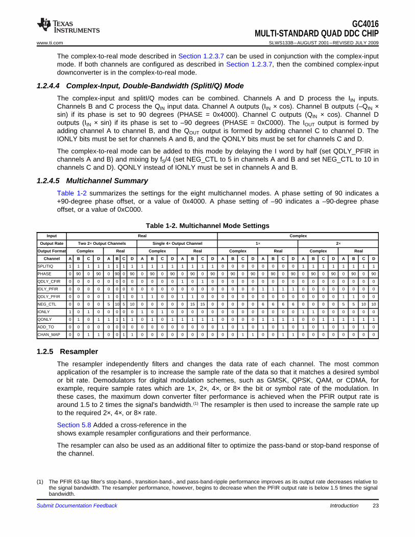
Table 1-2 summarizes the settings for the eight multichannel modes. A phase setting of 90 indicates a+90-degree phase offset, or a value of 0x4000. A phase setting of –90 indicates a –90-degree phaseoffset, or a value of 0xC000.
Table 1-2. Multichannel Mode SettingsInput Real Complex
Output Rate Two 2× Output Channels Single 4× Output Channel 1× 2×
Output Format Complex Real Complex Real Complex Real Complex Real
Channel A B C D A B C D A B C D A B C D A B C D A B C D A B C D A B C D
SPLITIQ 1 1 1 1 1 1 1 1 1 1 1 1 1 1 1 1 0 0 0 0 0 0 0 0 1 1 1 1 1 1 1 1
PHASE 0 90 0 90 0 90 0 90 0 90 0 90 0 90 0 90 0 90 0 90 0 90 0 90 0 90 0 90 0 90 0 90
QDLY_CFIR 0 0 0 0 0 0 0 0 0 0 0 0 1 0 1 0 0 0 0 0 0 0 0 0 0 0 0 0 0 0 0 0
IDLY_PFIR 0 0 0 0 0 0 0 0 0 0 0 0 0 0 0 0 0 0 0 0 1 1 1 1 0 0 0 0 0 0 0 0
QDLY_PFIR 0 0 0 0 1 0 1 0 1 1 0 0 1 1 0 0 0 0 0 0 0 0 0 0 0 0 0 0 1 1 0 0
NEG_CTL 0 0 0 0 5 10 5 10 0 0 0 0 0 15 15 0 0 0 0 0 6 6 6 6 0 0 0 0 5 5 10 10
IONLY 1 0 1 0 0 0 0 0 1 0 1 0 0 0 0 0 0 0 0 0 0 0 0 0 1 1 0 0 0 0 0 0
QONLY 0 1 0 1 1 1 1 1 0 1 0 1 1 1 1 1 0 0 0 0 1 1 1 1 0 0 1 1 1 1 1 1
ADD_TO 0 0 0 0 0 0 0 0 0 0 0 0 0 0 0 0 1 0 1 0 1 0 1 0 1 0 1 0 1 0 1 0
CHAN_MAP 0 0 1 1 0 0 1 1 0 0 0 0 0 0 0 0 0 0 1 1 0 0 1 1 0 0 0 0 0 0 0 0
The resampler independently filters and changes the data rate of each channel. The most commonapplication of the resampler is to increase the sample rate of the data so that it matches a desired symbolor bit rate. Demodulators for digital modulation schemes, such as GMSK, QPSK, QAM, or CDMA, forexample, require sample rates which are 1×, 2×, 4×, or 8× the bit or symbol rate of the modulation. Inthese cases, the maximum down converter filter performance is achieved when the PFIR output rate isaround 1.5 to 2 times the signal's bandwidth. (1) The resampler is then used to increase the sample rate upto the required 2×, 4×, or 8× rate.
Section 5.8 Added a cross-reference in theshows example resampler configurations and their performance.
The resampler can also be used as an additional filter to optimize the pass-band or stop-band response ofthe channel.
(1) The PFIR 63-tap filter's stop-band-, transition-band-, and pass-band-ripple performance improves as its output rate decreases relative tothe signal bandwidth. The resampler performance, however, begins to decrease when the PFIR output rate is below 1.5 times the signalbandwidth.
Submit Documentation Feedback Introduction 23

1.2.5.1 Functional Description
InputBuffer
FinalShiftand
Round
NDELAY NDEC
Interpolation Filter
FractionalDecimation
Resampling Filter
QTAP Filter Coefs
In Out
B0191-01
RATIO 226 NDECNDELAY
226 INPUT SAMPLE RATEOUTPUT SAMPLE RATE
(1-1)
GC4016MULTI-STANDARD QUAD DDC CHIPSLWS133B–AUGUST 2001–REVISED JULY 2009 www.ti.com
The resampler consists of an input buffer, an interpolation filter, and a final shift block. A functional blockdiagram of the resampler is shown in Figure 1-12.
The resampler sampling-rate change is the ratio NDELAY/NDEC, where NDELAY and NDEC are theinterpolation and decimation factors shown in Figure 1-12. The decimation amount NDEC is a mixedinteger/fractional number. When NDEC is an integer, then the exact sampling instance is computed andthere is no phase jitter. If NDEC is fractional, then the desired sampling instance will not be one of thepossible NDELAY interpolated values. Instead, the nearest interpolated sample is used. This introduces atiming error (jitter) of no more than 1/(2 × NDELAY) times the input sample period.
The input buffer accepts 24-bit data from the four input channels and adds them as necessary to formone, two, or four resampler channels (see the ADD_TO control bits in address 21 of the resampler controlpage). The input buffer serves both as a FIFO between the channels and the resampler, and as a datadelay line for the interpolation filter. The 64-complex-word input buffer can be configured as four segmentsof 16 complex words each to support four resampler channels, as two segments of 32 complex wordseach to support two resampler channels, or as a single segment of 64 complex words to support a singleresampler channel. The number of segments is set by NCHAN in address 16 of the resampler controlpage.
Figure 1-12. Resampler Channel Block Diagram
The interpolation filter zero-pads the input data by a factor of NDELAY and then filters the zero-paddeddata using a QTAP length filter. The output of the QTAP filter is then decimated by a factor of NDEC.
The resampling ratio for each channel is determined by setting the 32-bit RATIO controls in addresses 16through 31 of the resampler ratio page. The value of RATIO is defined as:
Up to four ratios can be stored within the chip. A ratio map register (address 23) selects which ratio isused by each channel.
The three spectral plots shown in Figure 1-13 illustrate the steps required to resample the channel data.The first spectral plot shows the data just after zero-padding. The sample rate after zero-padding isNDELAY × fS, where fS is the sample rate into the resampler. The second spectrum shows the shape ofthe QTAP filter which must be applied to the zero-padded data in order to suppress the interpolationimages. The last spectrum shows the final result after decimating by NDEC.
Introduction24 Submit Documentation Feedback

1.2.5.2 The Resampler Filter
GC4016MULTI-STANDARD QUAD DDC CHIP
www.ti.com SLWS133B–AUGUST 2001–REVISED JULY 2009
Figure 1-13(b) illustrates the spectral shape requirements of the QTAP filter. If the desired signalbandwidth is B, then the filter pass band must be flat out to B/2, and the filter's stop band must startbefore fS – B/2. The user designs this filter assuming a sample rate equal to NDELAY × fS. Section 5.8contains example resampler filter-coefficient sets. Other pass-band and stop-band responses can beused, such as root raised cosine receive filters, as desired. The resampler filter can also be used toaugment the CIC, CFIR, and PFIR filters' spectral response.
The number of filter coefficients, QTAP, is equal to NMULT × NDELAY, where NMULT is the number ofmultiplies available to compute each resampler output, and NDELAY is 4, 8, 16, 32, or 64, as described inSection 5.8. The maximum filter length is 512. The user specifies NMULT in address 17 of the resamplercontrol page.
The filter can be symmetric or non-symmetric, as selected by the NO_SYM_RES control in address 17 ofthe resampler control page. The symmetric filter is of even length, which means the center tap repeats.
The 12-bit filter coefficients are stored in a 256-word memory which can be divided into one, two, or fourequal blocks. This allows the user to store one symmetric filter of up to 512 taps, two symmetric filters ofup to 256 taps each, or four symmetric filters of up to 128 taps each. The number of filters is set byNFILTER in address 16 of the resampler control page. The filter used by each channel is selected usingthe FILTER_SEL controls in address 18 of the resampler control page. The filter lengths are cut in half ifthe filters are not symmetric. The coefficients are stored in memory with h0 stored in the lowest address,where h0 is the coefficient multiplied by the newest piece of data. The center tap of a symmetric filter ish(QTAP/2) – 1. The coefficients for multiple filters (NFILTER > 1), are interleaved in the 256-word memory.
Submit Documentation Feedback Introduction 25

NDELAY Images Added by Zero Padding
QTAP FilterFrequency Response
a) Spectrum After Zero Padding
Images Reducedby Filtering
Power
Power
Power
In-Band Aliasing Caused by Decimation by NDEC
Frequency
Frequency
Frequency
...
–3fS
–3fS
–fO –fO/2 fO/2 fO = (NDELAY/NDEC) fS
–2fS
–2fS
–fS/2
–fS/2
fS/2
fS/2
–fS
–fS
fS
fS
2fS
2fS
3fS
3fS
...
b) Spectrum After Filtering
......
c) Final Spectrum After Decimating by NDEC
M0063-01
1.2.5.3 Restrictions on NMULT
2 NO _ SYM_RESNDELAY FLOOR _ 2 256
NMULT NFILTER
-é ù= ´ê ú´ë û (1-2)
GC4016MULTI-STANDARD QUAD DDC CHIPSLWS133B–AUGUST 2001–REVISED JULY 2009 www.ti.com
Figure 1-13. The Resampler Spectral Response
The user does not directly set the value of NDELAY. The chip sets the value of NDELAY usingNO_SYM_RES, NMULT, and NFILTER according to:
where the function FLOOR_2[X] means the power-of-two value that is equal to or less than X. BecauseNMULT is restricted to be greater than or equal to 6 and less than or equal to 64, then NDELAY is 4, 8,16, 32, or 64. The length of the filter is then:
QTAP = (DELAY) (NMULT)
The value of NMULT determines both the length of the filter and the number of delays in the resamplingoperation. In general, one would choose the largest value of NMULT which gives an adequately largevalue of NDELAY. The choice of NMULT, however, must meet several restrictions. NMULT must begreater than a minimum, it cannot exceed the available number of multiplier cycles, and it must be lessthan the input delay line segment size. These restrictions are described as follows.
The minimum value of NMULT is determined by the minimum number of clock cycles required to updatethe resampler state. This is a hardware restriction imposed by the chip architecture. This limitation is:
NMULT ≥ if there are two or more outputsNMULT ≥ 7 if there is only one output
Introduction26 Submit Documentation Feedback

CKfNMULT 2
(OUTPUT _RATES)£ ´
S (1-3)
1.2.5.4 The Resampler Clock Divider
1.2.5.5 Final Shift and Round
( )FINAL _ SHIFTRES _ SUMRES _ GAIN 2
32,768 NDELAY
æ ö= ç ÷´è ø (1-4)
1.2.5.6 Bypassing the Resampler
GC4016MULTI-STANDARD QUAD DDC CHIP
www.ti.com SLWS133B–AUGUST 2001–REVISED JULY 2009
NMULT is the number of complex multiplier operations required to compute an output sample. Becausethe resampler can perform two multiplies every clock cycle, the value of NMULT cannot exceed two timesthe number of clock cycles available to the resampler for each channel. The number of clock cyclesavailable to the resampler is equal to the clock rate to the chip divided by the sum of the output samplerates for each resampler channel. Hence, NMULT must satisfy:
Note that the output sample rate of the resampler is usually much less than the clock rate, so that NMULTis rarely limited by this restriction.
NOTETHE NUMBER OF CLOCK CYCLES AVAILABLE TO THE RESAMPLER IS REDUCEDBY THE CLOCK DIVIDER, DISCUSSED IN Section 1.2.5.4.
The value of NMULT must also be less than the size of the delay line formed by the input buffer. The sizeof the delay line is 16 for four resampler channels, 32 for two channels, or 64 for a single channel, as setby the NCHAN control in address 16 of the resampler control page. This limits NMULT to be less than orequal to 15, 31, or 63, depending upon the number of resampler channels.
NOTEIf the resampler is being used at much less than its maximum capacity, i.e., NMULT ismuch less than twice the number of clock cycles available (See also RES_CLK_DIV),AND the channels are synchronous, then NMULT may equal the size of the delay line.
The typical resampler configuration has four active channels, all using the same filter and the sameresampling ratios. The typical configuration has NCHAN set to 4, NFILTER set to 1, NMULT set to 15, andNO_SYM_RES set to 0. This sets NDELAY to 32 and QTAPS to 480. See Section 5.8.
The resampler has a clock divider that can be used to reduce power consumption and to slow thecalculation rate of the resampler. The clock divider divides the internal clock by factors of one to 256 usingthe RES_CLK_DIV control in address 22 of the resampler control page. The clock divider reduces theresampler computational throughput, so care must be taken not to reduce the clock rate to the point thatthe computations can not be completed on time.
The gain of each resampler output is adjusted by an upshift by 0–15 bits (FINAL_SHIFT). This upshift isapplied just before rounding to the 12, 16, 20, or 24 MSBs (ROUND). The values of FINAL_SHIFT andROUND are set in control register 19 of the resampler control page. The resampler gain is:
where RES_SUM is the sum of the QTAP coefficients.
The resampler is bypassed by using a configuration which has h0 set to 1024, all other taps set to zero,NMULT set to 7, NO_SYM_RES set to 1, FINAL_SHIFT set to 5, and RATIO set to 226 (0x04000000).Note that the NDELAY term in the RES_GAIN equation shown in Equation 1-4 does not apply in this caseand should be set to unity in the gain equation.
Submit Documentation Feedback Introduction 27

1.2.5.7 Adaptive Ratio Change
1.2.6 Overall Gain
( )
( )
5 (SHIFT SCALE 6 BIG_SCALE 62) COARSE
FINAL_SHIFT
1 CFIR_SUMGAIN N 2 2
NZEROS 1 65,536
CFIR_SUM PFIR_SUM FINE_GAIN RES_SUM2
65,536 65,536 1024 32,768 NDELAY
+ + ´ -ì ü æ öæ ö= ´í ý ç ÷ç ÷+è ø è øî þ
æ öæ ö æ öæ öç ÷ç ÷ ç ÷ç ÷ ´è øè øè ø è ø (1-5)
1.2.7 Peak Counter
GC4016MULTI-STANDARD QUAD DDC CHIPSLWS133B–AUGUST 2001–REVISED JULY 2009 www.ti.com
The ratio maps (address 23) can be used to adjust dynamically each channel's resampling ratio. Fourdifferent ratios can be loaded into the chip. The ratio map indicates which ratio is to be used by whichchannel. This feature can be used to lock the resampling to a desired output timing by adaptively selectingratios which are slightly larger than, smaller than, or equal to the desired ratio. If the timing must beaccelerated, then the larger ratio is selected; if the timing is correct, then the exact ratio is used; and if thetiming must be retarded, then a smaller ratio is used. The ratio change can be synchronized using theRATIO_SYNC control in address 21.
The overall gain of the chip is a function of the amount of blanking (NZEROS), the decimationprogrammed into the chip (N), the scale circuit setting in the CIC filter (SHIFT, SCALE, and BIG_SCALE),the coarse gain setting (COARSE), the sum of the CFIR coefficients (CFIR_SUM), the sum of the PFIRcoefficients (PFIR_SUM), the fine gain (FINE_GAIN), the sum of the resampler coefficients (RES_SUM),the number of delays in the resampler filter (NDELAY) and the final shift (FINAL_SHIFT). The overall gainis shown in Equation 1-5. The term in braces should be less than or equal to unity. Note that the NDELAYterm is unity if the resampler is bypassed (see Section 1.2.5.6).
Unity gain is defined relative to the MSB of the I/O data. Unity gain means that a maximum dc input with atuning frequency of zero produces a maximum dc output, independent of the I/O words sizes.
Each channel has a peak counter which can monitor the input signal strength or can count the number ofoverflows detected at three points within the channel. The peak counter can count overflows due to theCOARSE_GAIN circuit, it can count overflows at the output from the CFIR, and it can count overflows atthe output of the PFIR.
If PEAK_MODE is set to 0 in address 28 of the channel control page, then the peak counter monitors thesignal strength at the input to the channel. The magnitude of each input sample is compared against athreshold selected by the PEAK_THRESH control in the same address. The threshold can be 1/4, 1/2,3/4, or full-scale. The peak counter increments each time the magnitude equals or exceeds the threshold.The input threshold crossings can be used in an AGC loop to optimize the input signal level to the ADC.
If PEAK_MODE is 1, then the peak counter monitors overflows at points selected by the PEAK_SELECTcontrol in address 26 of the channel control page. The peak counter increments each time an overflow isdetected. Note that the data value is saturated to plus or minus full scale, as appropriate, when theoverflow occurs. The overflow count can be used to check if the signal gain is set too high anywhere alongthe processing chain.
The counter counts up to 255 and stops. The counter value is saved in a holding register, and the counteris cleared by the sync selected by the PEAK_SYNC signal (see register 28). The sync can either be oneof the chip input syncs, a one-shot pulse, or the terminal count of the chip sync counter. A periodic syncallows the user to count threshold crossings or overflows during fixed time periods.
The user reads the count through the PEAK_COUNT control register at address 29 of the channel controlpage. The holding register contents are transferred to the PEAK_COUNT register a clock cycle after theuser reads the PEAK_COUNT register. This transfer is delayed to prevent the user from reading a peakcount value at the same time the circuit is updating the register.
Introduction28 Submit Documentation Feedback

1.2.8 Output Modes
GC4016MULTI-STANDARD QUAD DDC CHIP
www.ti.com SLWS133B–AUGUST 2001–REVISED JULY 2009
Note that there are two other points in the chip where overflows can occur. The first is at the input to theresampler, where samples from two channels can be added together as when processing complex inputdata. This may cause an overflow even though the samples feeding the resampler did not overflow. If anoverflow occurs here, the sample is saturated and a control bit in the status register (address 1) is set.The user can clear this bit by writing a 0 to the register. The control bit indicates that at least one sampleoverflowed since the last time the bit was cleared. Because the data path going into the resampler is 24bits, it is recommended that the gain be set such that this overflow never occurs. The second overflowpoint is at the resampler output. The user can check for these overflows by examining the chip output datafor maximum (saturated) values.
Data from the resampler can be output in one of several modes:• The microprocessor mode, where the outputs are read from the 8-bit control port• The wide-word microprocessor mode, where the outputs are read as 32-bit integers from a wide-word
control port• The synchronous serial mode, where the outputs are output through one or more of the four serial
ports• The asynchronous serial mode, where the channels are output on the same serial stream, but have
their own serial frame sync• The nibble mode, where the outputs are output in a 4-bit-at-a-time nibble serial format• The link mode, which is compatible with the 4-bit SHARC link port• The parallel mode, which outputs the data as 24-bit words
Only one mode is supported at a time. The output modes are controlled by writing to addresses 16through 26 within page 98 (the output control page).
A FIFO memory holds blocks of resampler output data, where each block contains one, two, or fourcomplex samples as specified by the BLOCK_SIZE control in address 20. The FIFO is used to buffer thedata rate between the resampler and the output. The number of blocks held in the FIFO depends on theoutput mode being used.
The data from the resampler can be rounded to 12, 16, 20, or 24 bits. The BITS_PER_WORD control inaddress 20 sets the serial-mode word size to be between 12 and 32 bits, or to set nibble and link-modewords to be either 16 or 32 bits. If the output word size is larger than the resampler output size, then theunused LSBs are cleared.
Tag bits (four bits per tag) may be programmed to replace the four LSBs of the specified output word size.The tags are used to identify the source of the data. The user can program eight different tag values inaddresses 23, 24, 25, and 26, two for each of the four complex output words. Tags are enabled using theTAG_EN control bit in address 17. A special 2-bit tag-mode control (TAG_22 in address 19 of theresampler control page) can be used to output 24-bit words containing 22 bits of data and 2 bits of tag.
The chip supports different decimation ratios and/or different resampling ratios for each channel. Ifdifferent ratios are used, or if the channels have not been synchronized using the DEC_SYNC controls(See Section 1.2.11), then the channels are asynchronous and tag bits are required in order to sort out thechannel data. If the same ratios are used, and the channels have been synchronized, then the output issynchronous and the tag bits are not required.
If the complex-to-real conversion modes of the PFIR described in Section 1.2.3.7 are used, then theREAL_ONLY control bit in address 18 can be used to output real rather than complex data. TheREAL_ONLY control can only be used if all of the channels are in the complex-to-real mode; a mix ofcomplex and real data is not allowed. If the complex output format is used to output real data(REAL_ONLY = 0), then the real outputs are output as the Q-half of the complex output words. The I-halfshould be ignored.
Submit Documentation Feedback Introduction 29

1.2.8.1 Microprocessor Mode
GC4016MULTI-STANDARD QUAD DDC CHIPSLWS133B–AUGUST 2001–REVISED JULY 2009 www.ti.com
The suggested control register settings for each of the output modes are shown in Table 1-3. Thesesettings assume all four channels are active and the outputs are synchronous.
The output circuitry is reset on power up. It is enabled by clearing the OUT_BLK_RESET andPAD_RESET bits in address 0. See Section 1.2.12 for the proper initialization procedures.
An output-block sync is provided (OUT_BLK_SYNC in address 17), which can be used to synchronize theserial clocks of multiple chips. See Section 1.2.12 for the proper synchronization sequences.
Table 1-3. Output Mode ControlsSuggested Default for Each Mode (Hex Values)
Micro- Wide-Word Serial Modes Nibble Link ParallelAddressControl Register processor Micro- Mode Mode Mode(Page 98) Four TDM Output AsynchronousMode processor Serial (Synchronous) ModeMode Outputs
3-state controls 16 02 FA 7F 7F (1) 7F (1) 7F (1) 7D FF
Output formats 17 40 40 40 40 40 40 48 40
Output modes 18 08 08 28 28 (2) 28 (2) 4A CB 6C
Output frame controls 19 00 00 01 07 (3) 01 07 00 00
Output word sizes 20 E8 E8 E9 EF 29 C8 08 E8 (4)
Output clocks 21 00 00 B1 01 01 01 01 01
Serial mux controls 22 00 00 E4 E4 E4 00 00 00
Output tag A 23 10 00 10
Output tag B 24 32 11 32
Output tag C 25 45 22 45
Output tag D 26 67 33 67
Miscellaneous 28 02 03 (5) 02
(1) For TDM serial or nibble modes, the master chip value should be 7F, and the the slave chip value should be 7D.(2) For TDM serial or nibble modes, the master chip value should be 28, and the the slave chip value should be 20.(3) For multichip modes, the frame length is set as described in Section 1.2.8.3.(4) For asynchronous parallel modes, set address 20 to 28.(5) Also set the RND22 control bit in address 19 (bit 6) of the resampler control page (page 64).
In the microprocessor mode (OUTPUT_MODE = 0 in address 18), the outputs are read in bytes from thecontrol port. The outputs are accessed by reading addresses 16 through 31 in pages 96 and 97.
The output FIFO buffers two blocks of complex samples in this mode. One block is accessed through themicroprocessor port as another block is being filled with new data. When the new block is filled, the FIFOswaps the blocks so that the user can access the new data. The block size is usually set to buffer fourcomplex samples per block (BLOCK_SIZE = 3). If only one or two channels are being output, then theblock size may be reduced, but it is suggested to keep it at four samples per block in order to reduce theinterrupt rate and to let the user read more samples after each interrupt.
When finished reading the block of data, the user sets the READY control bit in the status register(address 1). When the output FIFO has a new block of data ready, it clears the READY bit. If a block ofdata completes and the READY bit is not set, then the chip sets the MISSED control bit. The MISSED bitserves as a diagnostic, indicating that the processor was too slow and missed a block of data. Note thatthe rate at which the blocks are filled, and therefore the rate at which the data must be read from themicroprocessor port, depends on how fast the resampler can generate new output samples. When theresampler is interpolating, which is the resampler’s most commonly used mode, it generates multipleoutput samples each time it receives a sample from a downconverter channel. The user should use theresampler clock divider to slow its computation rate if the resampler is generating outputs too fast(SeeSection 1.2.5.4).
The RDY terminal can serve as an interrupt to inform the processor that a new block of samples is ready.The width and polarity of the RDY pulse is programmable (See EN_RDY in address16 and INV_RDY andRDY_WIDTH in address 17).
Introduction30 Submit Documentation Feedback

GC4016MULTI-STANDARD QUAD DDC CHIP
www.ti.com SLWS133B–AUGUST 2001–REVISED JULY 2009
The mapping of the output data into registers 16 through 31 depends on the OUTPUT_ORDER controlmode in address 21, the number of active channels, and whether the channels are synchronous orasynchronous.
If OUTPUT_ORDER = 0 and BLOCK_SIZE = 3, then each block contains the next four samples outputfrom the resampler. If the channels are synchronous, then the block contains one sample from eachchannel. If there are only two active channels, then the block contains two samples from each channel. Ifthere is only one active output channel, then the block contains four consecutive samples from the activechannel. If the channels are asynchronous, or if there are three active channels, then the output blockcontains the next four samples computed by the resampler. In this case, tags are required to separate thechannels. OUTPUT_ORDER = 0 must be used for asynchronous data.
If OUTPUT_ORDER = 1 or 2, then the channels are written into the FIFO using the channel number aspart of the address. In this mode, the previous block is complete when the Q-half of the output fromchannel A arrives. If the resampler ratio is the same integral value for all channels, then channels B, C,and D can be powered down and back up again while maintaining proper channel ordering. Channel Amay not be powered down, because it provides the Block Complete timing signal. OUTPUT_ORDERsettings of 1 and 2 are valid for synchronous channels, but NOT for asynchronous channels.
The following tables illustrate how the 24-bit channel outputs are mapped into addresses 16 through 31 ofpages 96 and 97. Note that addresses 16, 20, 24, and 28 are the unused LSBs of the 32-bit words andalways read back zero. Addresses 19, 23, 27, and 31 contain the MSBs of the output. In the 12-,16-, or20-bit output mode, all values are rounded into the MSBs and the unused LSBs are cleared. These tablesassume that BLOCK_SIZE = 3, which sets the block size to four complex words.
Table 1-4. Channel Output Map, Synchronous Four-Channel ModeADDRESSES OUTPUT_ORDER = 0 OUTPUT_ORDER = 1 OUTPUT_ORDER = 2
CHANNEL OUTPUT PAGE 9616, 17, 18, 19 AOUT, I-half AOUT, I-half AOUT, I-half20, 21, 22, 23 AOUT, Q-half BOUT, I-half BOUT, I-half24, 25, 26, 27 BOUT, I-half AOUT, Q-half COUT, I-half28, 29, 30, 31 BOUT, Q-half BOUT, Q-half DOUT, I-half
CHANNEL OUTPUT PAGE 9716, 17, 18, 19 COUT, I-half COUT, I-half AOUT, Q-half20, 21, 22, 23 COUT, Q-half DOUT, I-half BOUT, Q-half24, 25, 26, 27 DOUT, I-half COUT, Q-half COUT, Q-half28, 29, 30, 31 DOUT, Q-half DOUT, Q-half DOUT, Q-half
Table 1-5. Channel Output Map, Synchronous Two-Channel ModeADDRESSES OUTPUT_ORDER = 0 OUTPUT_ORDER = 1 OUTPUT_ORDER = 2
CHANNEL OUTPUT PAGE 9616, 17, 18, 19 A(i)OUT, I-half AOUT, I-half AOUT, I-half20, 21, 22, 23 A(i)OUT, Q-half BOUT, I-half BOUT, I-half24, 25, 26, 27 B(i)OUT, I-half AOUT, Q-half
Unused28, 29, 30, 31 B(i)OUT, Q-half BOUT, Q-half
CHANNEL OUTPUT PAGE 9716, 17, 18, 19 A(i+1)OUT, I-half AOUT, Q-half20, 21, 22, 23 A(i+1)OUT, Q-half BOUT, Q-half
Unused24, 25, 26, 27 B(i+1)OUT, I-half
Unused28, 29, 30, 31 B(i+1)OUT, Q-half
Submit Documentation Feedback Introduction 31

1.2.8.2 Wide-Word Microprocessor Mode
32-Bit Wide-Word Port
Parallel Port(Contains the 24-Bit Output Data)
Control Port(Reads Back Zero)
MSB LSB
P23 P0 C7 C0
M0064-01
GC4016MULTI-STANDARD QUAD DDC CHIPSLWS133B–AUGUST 2001–REVISED JULY 2009 www.ti.com
Table 1-6. Channel Output Map, Single-Channel ModeADDRESSES OUTPUT_ORDER = 0 OUTPUT_ORDER = 1 OUTPUT_ORDER = 2
CHANNEL OUTPUT PAGE 9616, 17, 18, 19 A(i)OUT, I-half AOUT, I-half AOUT, I-half20, 21, 22, 23 A(i)OUT, Q-half Unused24, 25, 26, 27 A(i+1)OUT, I-half AOUT, Q-half Unused28, 29, 30, 31 A(i+1)OUT, Q-half Unused
CHANNEL OUTPUT PAGE 9716, 17, 18, 19 A(i+2)OUT, I-half AOUT, Q-half20, 21, 22, 23 A(i+2)OUT, Q-half
Unused24, 25, 26, 27 A(i+3)OUT, I-half Unused28, 29, 30, 31 A(i+3)OUT, Q-half
In the complex-to-real conversion modes (seeSection 1.2.3.7), the real output is available in the Q portionof the registers, and the I portion is invalid. The REAL_ONLY control has no effect on the microprocessormode.
Table 1-4, Table 1-5 and Table 1-6 assume the block size control (BLOCK_SIZE in address 20) is set tofour samples. If the block size is two and OUTPUT_ORDER is 0, then page 97 is unused. If the block sizeis one and OUTPUT_ORDER is 0, then only addresses 16 through 23 of page 96 are used.
The wide-word microprocessor mode is selected by setting OUTPUT_MODE = 0 and by enabling theparallel output port (EN_P0 = EN_P1 = EN_P2 = EN_P3 = EN_PAR = 1 in address 16). The wide-wordmicroprocessor mode allows the user to read 32-bit words, rather than bytes. The 8-bit microprocessorport is augmented with the 24-bit parallel port to provide the 32-bit interface. The bit mapping into the32-bit port is shown in Figure 1-14.
Figure 1-14. Wide-Word Microprocessor Port
The channel outputs are read using addresses 16, 20, 24, and 28 of pages 96 and 97. The channelordering is the same as described in Section 1.2.8.1 and shown in Table 1-4, Table 1-5 and Table 1-6.
The upper 24 bits of the wide-word microprocessor port are read-only bits. The port and has the samecontrol and timing characteristics as shown in Figure 1-2 and Figure 1-3 for the normal microprocessorport.
Introduction32 Submit Documentation Feedback

1.2.8.3 Synchronous Serial Outputs
GC4016MULTI-STANDARD QUAD DDC CHIP
www.ti.com SLWS133B–AUGUST 2001–REVISED JULY 2009
The serial mode is selected by setting OUTPUT_MODE = 1, MASTER = 1 and enabling the serial outputterminals (EN_SCK = EN_SFS = EN_P0, 1, 2, 3 = 1 in address 16). The chip provides a bit serial clock(SCK), a frame strobe (SFS) and four data bit lines (SOUT A, B, C, and D) to output the data in a serialformat. The I and Q parts of complex outputs are always multiplexed onto the same bit-serial terminal. TheI-part is output first, MSB to LSB, followed by the Q-part. In the real mode (REAL_ONLY = 1), only the Qword per channel is output. The REAL_ONLY mode is used with the complex-to-real conversion mode ofthe PFIR.
The serial clock is the input clock (CK) divided by an integer value from 1 to 16, inclusive(SCK_RATE control in address 21). For even divisions, the serial clock changes on the rising edge of CK.The serial clock has a 50% duty cycle for all divisions. The polarity of the serial clock is programmable(which allows output data to be sampled on the rising or falling edge of SCK).
The serial output word size is programmable to be 12, 16, 20, 24, 28, or 32 bits per word(BITS_PER_WORD control in address 20). Note that the maximum word size out of the resampler is 24bits, so for output word sizes of 28 or 32 bits, the lower bits are always zero. For complex data outputs,pairs of words, each being 12 to 32 bits, are output.
Synchronous channel outputs can be transmitted as one channel per serial output on four separatebit-serial output terminals (SOUTA, SOUTB, SOUTC, and SOUTD), or multiplexed as two channels perterminal onto two output terminals (SOUTA and SOUTB), or multiplexed as all four channels on the sameterminal (SOUTA), as specified by the OUTPUT_ORDER and NSERIAL control bits in address 21. Thefour-channel (each on its own serial terminal) mode uses NSERIAL = 3 and OUTPUT_ORDER = 2. Thetwo-channels-per-terminal mode uses NSERIAL = 1 and OUTPUT_ORDER = 1. Thefour-channels-on-a-single-terminal mode uses NSERIAL = 0 and OUTPUT_ORDER = 0.
The serial streams SOUTA, SOUTB, SOUTC, and SOUTD are normally output on terminals P0, P1, P2,and P3, respectively. If required, the SMUX_0, SMUX_1, SMUX_2, and SMUX_3 controls in address 22can be used to select which stream is output on which of these terminals.
For synchronous channels, the FIFO block size (BLOCK_SIZE) should be set to match the number ofactive channels. If four channels are active, then BLOCK_SIZE should be set to 3. If two channels areactive, then BLOCK_SIZE should be set to 1. If only one channel is active, then BLOCK_SIZE should beset to 0.
The outputs are output in frames. Output frames start when the previous frame has completed AND a newdata block is ready in the FIFO (See BLOCK_SIZE above). The minimum output frame length can beprogrammed to be 1 to 64 words (up to 32 complex samples) using the FRAME_LENGTH control inaddress 19. Longer frame sizes can be used to time-division multiplex (TDM) channels from multiple chipsonto a signal serial bus or to smooth data flow when resampling.
The number of words output on each serial terminal during a frame can be programmed to be 1 to 8words (1 to 4 complex samples) using the WORDS_PER_FRAME control in address 20. TheWORDS_PER_FRAME control is usually set to match the number of active output channels multiplexedonto each serial terminal using the NSERIAL control. In real output modes, each sample is one word. Incomplex output modes, each sample is two words. NOTE: FRAME_LENGTH must be greater than orequal to WORDS_PER_FRAME.
If the selected number of words has been output, and the frame is not complete or a new FIFO block isnot ready, then the frame strobe (SFS) remains inactive, the data bits go into the high-impedance state,and the serial clock (SCK) continues. In this case, a new frame starts on the next SCK pulse after theframe completes and a new FIFO block is ready. If new outputs are ready before the previous frame isfinished, then the FIFO buffers the new data until the previous frame is complete. THE FRAME LENGTHAND SERIAL CLOCK RATES MUST BE SET SO THAT THE FRAME RATE IS GREATER THAN OREQUAL TO THE AVERAGE RESAMPLER OUTPUT RATE. This means that:
(Average # of clocks per resampler output) ≥ (Frame length)(bits per word)(clocks per bit)
Submit Documentation Feedback Introduction 33

1.2.8.4 Asynchronous Serial Outputs
GC4016MULTI-STANDARD QUAD DDC CHIPSLWS133B–AUGUST 2001–REVISED JULY 2009 www.ti.com
where the average # of clocks per resampler output is equal to:(Average # of clocks per resampler output) = (Channel decimation)(NDEC/NDELAY)
and NDEC/NDELAY is the resampling ratio (see Section 1.2).
The frame strobe signal (SFS) is programmable to come once per frame, once per complex word, or onceper word, using the SFS_MODE control in address 19. SFS is one SCK clock cycle wide and alwayscomes one SCK ahead of the first output bit in the transfer. Its polarity is programmable (INV_SFS inaddress 17). If the outputs are synchronous and the frame strobe signal is once per frame, then the wordposition in the frame relative to the SFS strobe can be used to identify which channel each samplebelongs to. If not, tags may be used to identify channels. Some processors require an SFS strobe witheach word so the position within a frame relative to the SFS strobe cannot be used to identify channels.Tag bits must be used for these processors, but may be turned off once synchronization has beenachieved. Note that frames can be generated back-to-back; specifically, the frame strobe can occur at thesame time as the last bit in the previous frame.
The serial frame timing is illustrated in Figure 1-15.
Synchronous data from multiple chips may be time-division multiplexed (TDM) onto the same serial bus. Amaster GC4016 chip (MASTER = 1 in address 18 and EN_RDY = 1 in address 16) provides the framestrobe signal and serial clock and an RDY start-of-frame pulse. The bidirectional RDY terminal is anoutput terminal from the master chip and is an input terminal for the slave chips (MASTER = 0,EN_RDY = 0). The slave chips use the RDY input frame strobe to identify the start of frame. The masterdrives the serial outputs for the first 1–8 words (WORDS_PER_FRAME) of the frame, and then puts itsserial-data outputin the high-impedance state. The slave chips are programmed using the FRAME_LENGTH control todelay the start of their outputs by 1–63 words from the beginning of frame. Note that the delay isprogrammed in words, NOT complex samples. The delay can be programmed independently for eachslave chip so that each chip can have its own block of time in which to output data. For example, afour-chip TDM stream can be generated, where each chip is outputting eight words (four complexoutputs), by setting WORDS_PER_FRAME = 7 (8 words per chip) in all four chips,FRAME_LENGTH = 31 in the master chip (32 words per frame), FRAME_LENGTH = 7 in the second chip(start at word 8), FRAME_LENGTH = 15 in the third chip (start at word 16), and FRAME_LENGTH = 23 inthe fourth chip (start at word 24).
The TDM mode requires that the serial clocks in the master and slave chips have been synchronizedusing the OUT_BLK_SYNC control. See Section 1.2.12 for details.
The TDM mode is intended for use with a single serial output stream (NSERIAL = 0), but also works withone, two, or four streams. The TDM outputs are then identified within each stream, according to theNSERIAL and OUTPUT_ORDER controls as shown in Figure 1-15(c).
Asynchronous channels must be output on a single serial stream. Tag bits or separate frame strobes mustbe used to identify the channels. In the asynchronous mode, each channel sample is output as a serialword (or complex pair) as soon as the resampler has finished generating it. Tag bits or separate framestrobes are used to match the serial output word with the channel it came from. Asynchronous channelsmust use NSERIAL = 0, OUTPUT_ORDER = 0, and BLOCK_SIZE = 0. WORDS_PER_FRAME andFRAME_LENGTH must be set to 0 for real data and 1 for complex data. Four-bit tags are enabled bysetting TAG_EN = 1 and TAG_22 = 0. The 2-bit tag mode (TAGEN = 0, TAG22 = 1) can be used to output24-bit words that are 22 bits of data plus 2 bits of tag.
Separate frame strobes are enabled by using the 2-bit tag mode and setting the EN_4_FS control bit
Introduction34 Submit Documentation Feedback

GC4016MULTI-STANDARD QUAD DDC CHIP
www.ti.com SLWS133B–AUGUST 2001–REVISED JULY 2009
(address 28 of the output page). When the EN_4_FS bit is set, the 2-bit tag is used to generate the fourframe strobes FSA (tag = 0), FSB (tag = 1), FSC (tag = 2) and FSD (tag = 3). The timing for these framestrobes is the same as shown for SFS in Figure 1-15. The separate frame strobe mode (TAG_22 = 1 andEN_4_FS = 1) is valid for all serial word sizes, but the 2-bit tag is only output for 24-, 28-, or 32-bit serialword sizes. The four frame strobes share output terminals P4, P5, P6, and P7.
Submit Documentation Feedback Introduction 35

The Data Pins Go High-Impedance After the Last Bit
SCK
SFS
SOUT
SOUTA
SOUTA
SOUTA
SOUTB
SOUTB
SOUTC
SOUTD
SFS
SFS
SFS
(b) SFS_MODE = 2: One Frame Sync at the Start of Each Complex Word
© One-, Two-, or Four-Channel Mux Modes (The Timing Shown is for SFS_MODE = 2 and BLOCK_SIZE = 3)
I15 I14 I1 I0 Q15 Q14 Q1 Q0
SCK
SFS
SOUT
(a) SFS_MODE = 3: Frame Sync at the Start of Each Word (16-Bit Words Shown)
I15 I14 I1 I0 Q15 Q14 Q1 Q0
Clock is Continuous
IA
IA
IA IA
IA
IA
IB
IB
IB IB
IB
IB
IC
IC
IC IC
IC
IC
ID
ID
ID
ID
ID
QA
QA
QA QA
QA
QA
QB
QB
QB QB
QB
QB
QC
QC
QC QC
QC
QC
QD
QD
QD
QD
QD
The Minimum Output Frame Length is Set by FRAME_LENGTH
Four Output Streams: NSERIAL = 3, WORDS_PER_FRAME = 1, OUTPUT_ORDER = 2
Two Output Streams: NSERIAL = 1, WORDS_PER_FRAME = 3, OUTPUT_ORDER = 1
Single Output Stream: NSERIAL = 0, WORDS_PER_FRAME = 7, OUTPUT_ORDER = 0
T0172-01
1.2.8.5 Nibble-Mode Output
GC4016MULTI-STANDARD QUAD DDC CHIPSLWS133B–AUGUST 2001–REVISED JULY 2009 www.ti.com
Figure 1-15. Serial Output Formats
The four serial output terminals (P0, P1, P2, and P3), the serial clock terminal (SCK), and the frame syncterminal (SFS) can be configured as a nibble-wide output by setting OUTPUT_MODE = 2, MASTER = 1,
Introduction36 Submit Documentation Feedback

1.2.8.6 Link-Mode Output
GC4016MULTI-STANDARD QUAD DDC CHIP
www.ti.com SLWS133B–AUGUST 2001–REVISED JULY 2009
and NIBBLE = 1 in address 18. These terminals are in a high-impedance state when the chip powers upand must be enabled by setting EN_SCK, EN_SFS, EN_P0, EN_P1, EN_P2, and EN_P3 in address 16.The nibble mode functions the same as the serial mode except 4 bits are output at a time, the word size isrestricted to being 16 or 32 bits, all channels are output on the same nibble port, and the SFS signal iscoincident with the first nibble of a transfer, rather than being one SCK clock early.
The nibble mode requires that OUTPUT_ORDER = 0 and NSERIAL = 0.
For synchronous channels, BLOCK_SIZE should be set to the number of active channels,WORDS_PER_FRAME should be set to match the number of active words (two per active channel forcomplex data), and FRAME_LENGTH should be set to define the minimum number of words per frame.
Asynchronous channels must use BLOCK_SIZE = 0 and TAG_EN = 1. WORDS_PER_FRAME must beset to 0 for real data and 1 for complex data.
The nibble mode can support TDM of multiple chips, in which case the RDY terminal is used tosynchronize master and slave chips in the same way it was used in the serial TDM mode. To use theTDM mode, set MASTER = 1 and EN_RDY = 1 in the master chip, and set MASTER = 0 andEN_RDY = 0 in the slave chips.
The SFS strobe behaves the same in the nibble mode as in the serial mode, except that the SFS strobe iscoincident with the first nibble in the word and that the SFS strobe cannot be outputevery word in the real 16-bits-per-word mode (REAL_ONLY = 1, BITS_PER_WORD = 0). The latterexception means that for 16-bit real data, SFS_MODE must be equal to 0 (one SFS strobe at thebeginning of the frame) AND the frame length cannot be one word (FRAME_LENGTH cannot equal 0).This restriction does not apply to complex outputs or to 32-bit nibble-output modes.
The separate frame strobe mode described for asynchronous serial data can also be used in the nibblemode.
The nibble-output mode, for 16-bit data (BITS_PER_WORD = 0), requires the SCK_RATE (SCK outputclock division) value to be >0. This limitation affects decimation values of 36 through 60.
The four serial output terminals (P0, P1, P2, and P3) and the serial clock (SCK) and RDY terminals canbe configured as a nibble-wide link port by setting OUTPUT_MODE = 2, NIBBLE = 1, and LINK = 1 inaddress 18. The link port can feed an ADSP-2106x SHARC DSP chip's link port. The P0, P1, P2, P3, andSCK terminals are in a high-impedance state when the chip powers up and must be enabled by settingEN_SCK, EN_P0, EN_P1, EN_P2, and EN_P3 in address 16. EN_RDY must be low. In the link mode, theRDY output terminal becomes the ACK (acknowledge) input terminal, which is tied to the link port LACKsignal. LACK is used to stall the output until the processor is ready for it.
The outputs are transmitted in 4-bit nibbles on the rising edge of SCK (INV_SCK in address 17 must below). If the ACK signal is low at the end of a 32-bit transfer, then the clock remains high and thetransmission of the next word is delayed until ACK goes high again.
The link port transfers data as 32-bit packets. The user can choose to transmit two 16-bit words perpacket or a single 32-bit word. To transmit two 16-bit words per packet, the user must setBITS_PER_WORD to 0 and WORDS_PER_FRAME to 1. To transmit a single 32-bit word per packet, theuser must set BITS_PER_WORD to 1 and WORDS_PER_FRAME to 0.
The link mode requires OUTPUT_ORDER, NSERIAL, and BLOCK_SIZE to be set to 0. FRAME_LENGTHand SFS_MODE are unused and should also be set to 0. The link-mode clock rate is set by SCK_RATE.
If the outputs are synchronous, and the chip has been initialized properly (see Section 1.2.12), then thefirst transfer is the I part of channel A followed by the Q part, followed by the I/Q pairs from channels B, C,and D. If the channels are asynchronous, or initialization is not possible, then tag bits must be used toidentify the channel data. The tag bits for synchronous data may be disabled once synchronization isachieved.
Submit Documentation Feedback Introduction 37

1.2.8.7 Parallel-Mode Output
GC4016MULTI-STANDARD QUAD DDC CHIPSLWS133B–AUGUST 2001–REVISED JULY 2009 www.ti.com
The link mode normally puts the least-significant bit in P0. Note that this is opposite of the GC4014. Forterminal compatibility with the GC4014, the control SMUX_0 in address 22 should be set to 1. This putsthe least-significant bit in P3.
When transferring two 16-bit words in a 32-bit link packet, the first word ends up in the upper 16 bits of thepacket and the second word in the lower 16 bits. This means that the memory order in the DSP chip mayend up being QA, IA, QB, IB, ... for complex data and I1, I0, I3, I2, ... for single-channel real data. TheREVERSE_IQ control bit in address 18 eliminates this problem by swapping the I/Q pair (or the I0/I1 pair)in the 32-bit packet.
The SCK, SFS, RDY, and P0 through P23 terminals are used in the parallel mode to output 24-bit-widedata samples. The mode is enabled by setting the EN_SCK, EN_SFS, EN_RDY, EN_P0, EN_P1, EN_P2,EN_P3, and EN_PAR bits in address 16, and by setting OUTPUT_MODE = 3, MASTER = 1, andPARALLEL = 1 in address 18. The parallel mode also requires NSERIAL = 0 and OUTPUT_ORDER = 0in address 21. FRAME_LENGTH is unused and should be set to 0 in address 20.
The 24-bit samples are clocked out on the rising edge SCK (or the falling edge if INV_SCK is set). TheSCK clock is continuous, and the SFS and RDY outputs are used identify when a valid sample has beenclocked out. The data-valid flags go high during the SCK clock period when the 24-bit sample is valid. TheSFS and RDY flags behave in two modes as controlled by the SFS_MODE control bits in address 19.
If SFS_MODE is 0 or 1, then SFS is IVALID and RDY is QVALID. If the outputs are synchronous, and thechip has been initialized properly (see Section 1.2.12), then the first valid sample after initialization is the Ipart of channel A. The next valid sample is the Q part, followed by the I/Q pairs from channels B, C, andD. If the channels are asynchronous, or initialization is not possible, then tag bits must be used to identifythe channel data. The tag bits for synchronous data may be disabled once synchronization is achieved.
If SFS_MODE is 2 or 3, then SFS is a data-valid flag (I or Q) and the RDY output is a start-of-frame flagwhich identifies the I part of channel A. If the outputs are synchronous, then the channel data can beidentified by its position in the frame relative to the RDY flag. If the outputs are asynchronous, then tagsmust be used to identify the channel data. The parallel output timing is illustrated in Figure 1-16. Note thatwhen SFS_MODE is 2 or 3, the RDY flag goes high at the end of the frame and goes low after the firstword of the next frame. This is illustrated in Figure 1-16 (b) and (d).
The polarities of the SFS and RDY flags are controlled by the INV_SFS and INV_RDY bits in address 17.
Introduction38 Submit Documentation Feedback

SCK
RDY (Q Valid)
SFS (I Valid)
P[0:23]
(a) Synchronous Channels, SFS_MODE = 0, BLOCK_SIZE = 3
AQ0 BI0 BQ0 CI0 CQ0 DI0 DQ0 AQ1AI1 BI1AI0
SCK
RDY (Q Valid)
SFS (I Valid)
P[0:23]
(c) Asynchronous Channels, SFS_MODE = 0, BLOCK_SIZE = 0
AQ0 BI0 BQ0 CQ0CI0AI0
SCK
P[0:23]
(d) Asynchronous Channels, SFS_MODE = 2, BLOCK_SIZE = 0
AQ0 BI0 BQ0 CQ0CI0AI0
T0173-01
SCK
RDY(Fram Start)
RDY(Fram Start)
SFS(I or Q Valid)
SFS(I or Q Valid)
P[0:23]
(b) Synchronous Channels, SFS_MODE = 2, BLOCK_SIZE = 3
AQ0 BI0 BQ0 CI0 CQ0 DI0 DQ0 AQ1AI1 BI1AI0
1.2.9 Clocking
GC4016MULTI-STANDARD QUAD DDC CHIP
www.ti.com SLWS133B–AUGUST 2001–REVISED JULY 2009
Figure 1-16. Parallel-Mode Timing
The clock rate is equal to the input data rate, which can be up to 100 MHz. An internal clock doubler doubles the clock rate so that the internal circuitry is clocked at twice the datarate. The clock doubler requires a continuous clock (no deleted clock pulses) to proper operation.
Submit Documentation Feedback Introduction 39

1.2.10 Power-Down Modes
1.2.11 Synchronization
GC4016MULTI-STANDARD QUAD DDC CHIPSLWS133B–AUGUST 2001–REVISED JULY 2009 www.ti.com
The DVAL input is used as an active-low data-valid signal which is clocked into the chip on the rising edgeof CK. The data in the next CK cycle is ignored when DVAL is high. The DVAL signal operates by gatingthe output of the clock doubler. It does not affect the clock to the output circuitry, so the output continueswhile DVAL is high. The DVAL signal allows users to input data in bursts, such as data which is beingread from a memory or FIFO. The DVAL signal should never be high for more than 1 ms. Normally, DVALis grounded.
The clock doubler can be bypassed, and an externally generated 2× clock can be used in its place, bysetting the CK_2X_EN control bit in address 0. In this mode, the DVAL terminal becomes the externalCK_2X input. This mode is intended for test purposes only.
The CK_2X_TEST control bit in address 0 enables the clock-test mode, where the internal doubled clockis output on the SO terminal. The DVAL terminal must be low in this test mode.
The chip has a power-down and clock-loss-detect circuit. This circuit detects if the clock is absent longenough to cause dynamic storage nodes to lose state. If clock loss is detected, an internal reset state isentered to force the dynamic nodes to become static. The control registers are not reset and retain theirvalues, but any data values within the chip are lost. When the clock returns to normal, the chipautomatically returns to normal. In the reset state, the chip consumes only a small amount of standbypower. The user can select whether this circuit is in the automatic clock-loss-detect mode, is always on(power-down mode), or is disabled (the clock reset never kicks in) using the CK_LOSS_DETECT andGLOBAL_RESET control bits in address 0. The whole chip or individual downconverter channels can bepowered down.
NOTEResampler channel 0 provides the block complete signal to the output FIFO whenOUTPUT_ORDER = 1 or 2. This means that the channel feeding resampler channel 0,typically channel A (see CHAN_MAP in the resampler control page), cannot be powereddown when OUTPUT_ORDER = 1 or 2.
Each GC4016 chip can be synchronized through the use of one of two sync input signals, an internalone-shot sync generator or a sync counter. The sync to each circuit can also be set to be always on oralways off. Each circuit within the chip, such as the sine/cosine generators or the decimation controlcounter can be synchronized to one of these sources. These syncs can also be output from the chip sothat multiple chips can be synchronized to the syncs coming from a designated master GC4016 chip.
The 3-bit sync mode control for each sync circuit is defined in Table 1-7.
Table 1-7. Sync ModesMODE SYNC SOURCE
0, 1 Off (never asserted)2 SIA3 SIB4 ONE_SHOT5 TC (terminal count of internal counter)6, 7 On (always active)
Introduction40 Submit Documentation Feedback

GC4016MULTI-STANDARD QUAD DDC CHIP
www.ti.com SLWS133B–AUGUST 2001–REVISED JULY 2009
NOTEThe internal syncs are active-high. The SIA and SIB inputs have been inverted to be theactive-high syncs SIA and SIB in Table 1-7.
The ONE_SHOT can either be a level or a pulse, as selected by the OS_MODE control bit. The levelmode is used to initialize the chip, the pulse mode is used to synchronously switch frequency, phase, orgain values.
Typically, the decimation counters (DEC_SYNC), the flush circuits (FLUSH_SYNC), and the output blocksync (OUT_BLK_SYNC) are set to SIA, whereas the NCO phase-accumulator syncs (NCO_SYNC) areset to SIB. The SIA input can then be used to initialize and flush the channels and the SIB sync input canbe used, if desired, to synchronize the phases of the NCOs.
The recommended sync mode settings are summarized in Table 1-8.
The SIA and SIB sync inputs are either connected to a user-defined sync generator, for example, anFPGA, or are tied to a GC4016 chip's sync output terminal (SO). If there are multiple GC4016 chips in thesystem, then the SO terminal of one chip can be used to drive the SIA input of all chips, and the SOterminal of another chip can drive the SIB inputs of all chips.
Submit Documentation Feedback Introduction 41
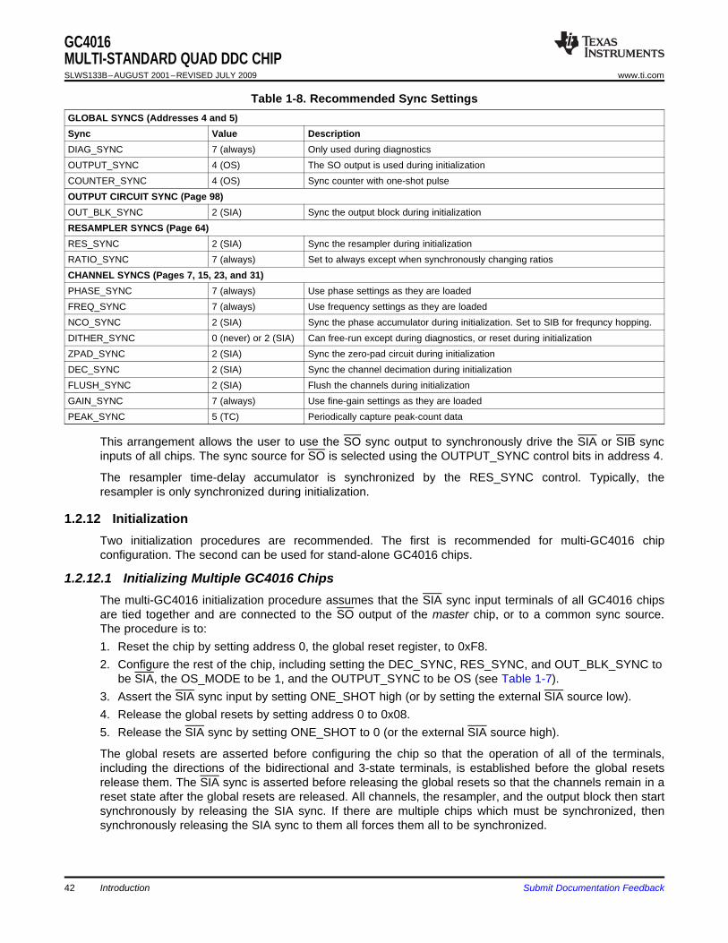
1.2.12 Initialization
1.2.12.1 Initializing Multiple GC4016 Chips
GC4016MULTI-STANDARD QUAD DDC CHIPSLWS133B–AUGUST 2001–REVISED JULY 2009 www.ti.com
Table 1-8. Recommended Sync SettingsGLOBAL SYNCS (Addresses 4 and 5)Sync Value DescriptionDIAG_SYNC 7 (always) Only used during diagnosticsOUTPUT_SYNC 4 (OS) The SO output is used during initializationCOUNTER_SYNC 4 (OS) Sync counter with one-shot pulseOUTPUT CIRCUIT SYNC (Page 98)OUT_BLK_SYNC 2 (SIA) Sync the output block during initializationRESAMPLER SYNCS (Page 64)RES_SYNC 2 (SIA) Sync the resampler during initializationRATIO_SYNC 7 (always) Set to always except when synchronously changing ratiosCHANNEL SYNCS (Pages 7, 15, 23, and 31)PHASE_SYNC 7 (always) Use phase settings as they are loadedFREQ_SYNC 7 (always) Use frequency settings as they are loadedNCO_SYNC 2 (SIA) Sync the phase accumulator during initialization. Set to SIB for frequncy hopping.DITHER_SYNC 0 (never) or 2 (SIA) Can free-run except during diagnostics, or reset during initializationZPAD_SYNC 2 (SIA) Sync the zero-pad circuit during initializationDEC_SYNC 2 (SIA) Sync the channel decimation during initializationFLUSH_SYNC 2 (SIA) Flush the channels during initializationGAIN_SYNC 7 (always) Use fine-gain settings as they are loadedPEAK_SYNC 5 (TC) Periodically capture peak-count data
This arrangement allows the user to use the SO sync output to synchronously drive the SIA or SIB syncinputs of all chips. The sync source for SO is selected using the OUTPUT_SYNC control bits in address 4.
The resampler time-delay accumulator is synchronized by the RES_SYNC control. Typically, theresampler is only synchronized during initialization.
Two initialization procedures are recommended. The first is recommended for multi-GC4016 chipconfiguration. The second can be used for stand-alone GC4016 chips.
The multi-GC4016 initialization procedure assumes that the SIA sync input terminals of all GC4016 chipsare tied together and are connected to the SO output of the master chip, or to a common sync source.The procedure is to:1. Reset the chip by setting address 0, the global reset register, to 0xF8.2. Configure the rest of the chip, including setting the DEC_SYNC, RES_SYNC, and OUT_BLK_SYNC to
be SIA, the OS_MODE to be 1, and the OUTPUT_SYNC to be OS (see Table 1-7).3. Assert the SIA sync input by setting ONE_SHOT high (or by setting the external SIA source low).4. Release the global resets by setting address 0 to 0x08.5. Release the SIA sync by setting ONE_SHOT to 0 (or the external SIA source high).
The global resets are asserted before configuring the chip so that the operation of all of the terminals,including the directions of the bidirectional and 3-state terminals, is established before the global resetsrelease them. The SIA sync is asserted before releasing the global resets so that the channels remain in areset state after the global resets are released. All channels, the resampler, and the output block then startsynchronously by releasing the SIA sync. If there are multiple chips which must be synchronized, thensynchronously releasing the SIA sync to them all forces them all to be synchronized.
Introduction42 Submit Documentation Feedback

1.2.12.2 Initializing Stand-Alone GC4016 Chips
1.2.13 Data Latency
1.2.14 Diagnostics
1.2.15 JTAG
1.2.16 Mask Revision Register
GC4016MULTI-STANDARD QUAD DDC CHIP
www.ti.com SLWS133B–AUGUST 2001–REVISED JULY 2009
The initialization sequence for a stand-alone GC4016 chip is similar to the one for the multi-GC4016procedure, except that the ONE_SHOT is used to synchronize the chip, not the SIA input sync. Theprocedure is to:1. Reset the chip by setting address 0, the global reset register, to 0xF8.2. Configure the rest of the chip, including setting the DEC_SYNC, RES_SYNC, and OUT_BLK_SYNC to
be ONE_SHOT (mode 4) and the OS_MODE to be 1.3. Assert the syncs by setting ONE_SHOT high.4. Release the global resets by setting address 0 to 0x08.5. Release the syncs by setting ONE_SHOT to 0.
The data latency through the chip is defined as the delay from the rising edge of a step-function chip inputto the rising edge of the step function as it leaves the chip. This delay is dominated by the number of tapsin each of the filters. An estimate of the overall latency through the chip, expressed as the number of inputclock cycles is:
(CIC latency = 2.5N) + (CFIR latency = 0.5N × CTAP) + (PFIR latency = N × PTAP) +(Resampler latency = 2N × NMULT) + (Output delay) + (Pipeline delay)
where N is the CIC decimation ratio, CTAP is the number of CFIR taps, and PTAP is the number of PFIRtaps. CTAP and PTAP are normally 21 and 63. Latency can be reduced by using the NO_SYM_CFIR andNO_SYM_PFIR modes to shorten these filters. The latency in the resampler can be minimized by usingthe bypass configuration (see Section 1.2.5.6).
The output delay depends on the output mode, but is approximately equal to the FIFO block size(BLOCK_SIZE + 1) times the output sample period. The pipeline delay is approximately 40 clock cycles.
The chip has an internal ramp generator which can be used in place of the data inputs for diagnostics. Aninternal checksum circuit generates a checksum of the output data to verify chip operation. Section 5.14gives suggested checksum configurations and their expected checksums.
Besides the internal diagnostics, the chip can support board-level testing. An output test configuration,which can help initial debug as well as production test, is described in Section 5.15.
The GC4016 supports a four-terminal (TDI, TDO, TCK, and TMS) boundary-scan interface. The GC4016BSDL file can be downloaded from http://focus.ti.com/docs/toolsw/folders/print/gc4016dk.html#description(SLWC006).
An 8-bit mask-revision code (REVISION) can be read from address 27 of the output control page (page98). The revision code allows users to determine, through software, what version of the GC4016 chips isbeing used. The current mask revision codes are shown in Table 1-9.
Table 1-9. Mask RevisionsGC4016
Revision Code Release Date Mask Code on Description(REVISION) Package
0 April 2000 SAMPLE Early samples1 September 2000 1001ACBA First release, has 40-Ω Vcore-to-Vpad short, no JTAG
Submit Documentation Feedback Introduction 43
2 Packaging
2.1 GC4016PB 160-Ball Plastic Ball-Grid Array (PBGA)
GC4016MULTI-STANDARD QUAD DDC CHIPSLWS133B–AUGUST 2001–REVISED JULY 2009 www.ti.com
Table 1-9. Mask Revisions (continued)GC4016
Revision Code Release Date Mask Code on Description(REVISION) Package
2 March 2001 1001ACBB Production release, JTAG added, short removed.
Schematic symbols and terminal assignments for the GC4016 in each of its input configurations areshown in Figure 2-1.
Packaging44 Submit Documentation Feedback
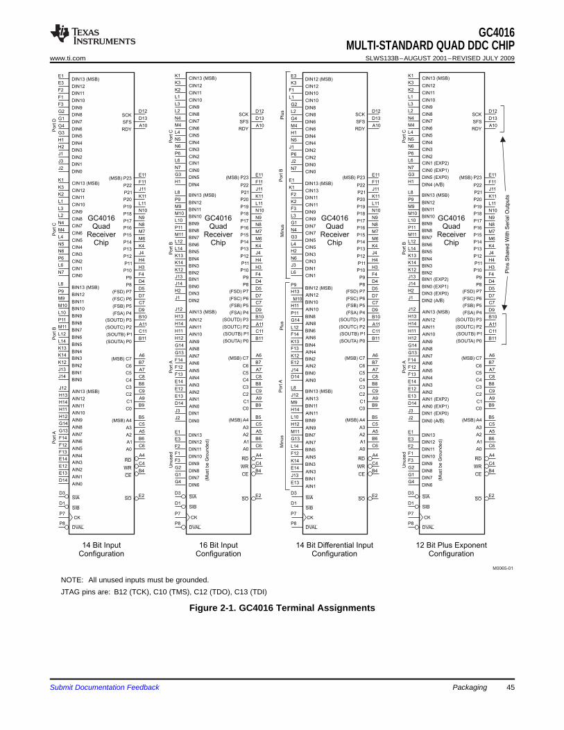
AIN13 (MSB)J12
AIN12H13
AIN11H14
AIN10H11
AIN9H12
AIN8G14
AIN7G13
AIN6F14
AIN5F12
AIN4F13
D1
CKP7
E2
(MSB) C7A6
C6B7
C5A7
C4C8
C3B8
C2C9
C1A9
C0B9
B4
(MSB) A4B5
A3C5
A2A5
GC4016Quad
ReceiverChip
GC4016Quad
ReceiverChip
GC4016Quad
ReceiverChip
GC4016Quad
ReceiverChip
SCKD12
SFSD13
RDYA10
A1B6
A0C6
C4
A4
AIN3E14
AIN2E12
AIN1E13
AIN0D14
P8
BIN13 (MSB)L8
BIN12P9
BIN11M9
BIN10M10
BIN9L10
BIN8P11
BIN7M11
BIN6L12
BIN5L14
BIN4K13
BIN3K14
BIN2K12
BIN1J13
BIN0J14
CIN13 (MSB)K1
CIN12K3
CIN11K2
CIN10L1
CIN9L3
CIN8L2
CIN7N4
CIN6M4
CIN5L4
CIN4N5
CIN3N6
CIN2P6
CIN1L6
CIN0N7
DIN13 (MSB)E1
DIN12E3
DIN11F2
DIN10F1
DIN9F3
DIN8G2
DIN7G1
DIN6G4
DIN5G3
DIN4H1
DIN3H2
DIN2J1
DIN1J3
DIN0J2
D3
P13K4
P12J4
P11H4
P10H3
P9F4
P8D4
(FSD) P7D5
(FSC) P6D7
(FSB) P5C7
(FSA) P4D9
B10
A11
C11
B11
(MSB) P23E11
P22F11
P21J11
P20K11
P19L11
P18N10
P17N9
P16N8
P15M7
P14M6
14 Bit InputConfiguration
16 Bit InputConfiguration
14 Bit Differential InputConfiguration
12 Bit Plus ExponentConfiguration
AIN13J12
AIN12H13
AIN11H14
AIN10H11
AIN9H12
AIN8G14
AIN7G13
AIN6F14
AIN5F12
AIN4F13
D1
CKP7
AIN3E14
AIN2E12
AIN1E13
AIN0D14
P8
BIN13 (MSB)L8
BIN12 (MSB)P9
BIN11M9
BIN10M10
BIN9L10
BIN8P11
BIN7M11
BIN6L12
BIN5L14
BIN4K13
BIN3K14
BIN2K12
BIN1J13
BIN0J14
CIN13K1
CIN12K3
CIN11K2
CIN10L1
CIN9L3
CIN8L2
CIN7N4
CIN6M4
CIN5L4
CIN4N5
CIN3N6
CIN2P6
CIN1L6
CIN0N7
DIN13 (MSB)E1
DIN12 (MSB)E3
DIN11F2
DIN10F1
DIN9F3
DIN8G2
DIN7G1
DIN6G4
DIN5G3
DIN4H1
DIN3H2
DIN2J1
DIN1J3
DIN0J2
D3
SIBSIB SIBD1D1
CKCKP7P7
E2E2E2SOSOSO
(MSB) C7(MSB) C7(MSB) C7A6A6A6
C6C6C6B7B7B7
C5C5C5A7A7A7
C4C4C4C8C8C8
C3C3C3B8B8B8
C2C2C2C9C9C9
C1C1C1A9A9A9
C0C0C0B9B9B9
CECECEB4B4B4
(MSB) A4(MSB) A4(MSB) A4B5B5B5
A3A3A3C5C5C5
A2A2A2A5A5A5
SCKSCKSCKD12D12D12
SFSSFSSFSD13D13D13
RDYRDYRDYA10A10A10
A1A1A1B6B6B6
A0A0A0C6C6C6
WRWRWRC4C4C4
RDRDRDA4A4A4
DVALDVAL DVALP8P8
SIASIA SIAD3D3
P13P13P13K4K4K4
P12P12P12J4J4J4
P11P11P11H4H4H4
P10P10P10H3H3H3
P9P9P9F4F4F4
P8P8P8D4D4D4
(FSD) P7(FSD) P7(FSD) P7D5D5D5
(FSC) P6(FSC) P6(FSC) P6D7D7D7
(FSB) P5(FSB) P5(FSB) P5C7C7C7
(FSA) P4(FSA) P4(FSA) P4D9D9D9
B10B10B10
A11A11A11
C11C11C11
B11B11B11
(MSB) P23(MSB) P23(MSB) P23
Pin
s S
hare
d W
ith S
erial O
utp
uts
E11E11E11
P22P22P22F11F11F11
P21P21P21J11J11J11
P20P20P20K11K11K11
P19P19P19L11L11L11
P18P18P18N10N10N10
P17P17P17N9N9N9
P16P16P16N8N8N8
P15P15P15M7M7M7
P14P14P14M6M6M6
AIN13 (MSB)AIN13 (MSB)J12J12
AIN12AIN12H13H13
AIN11AIN11H14H14
AIN10AIN10H11H11
AIN9AIN9H12H12
AIN8AIN8G14G14
AIN7AIN7G13G13
AIN6AIN6F14F14
AIN5AIN5F12F12
AIN4AIN4F13F13
AIN3AIN3E14E14
AIN2AIN2E12E12
AIN1 (EXP2)AIN1E13E13
AIN0 (EXP1)AIN0D14D14
BIN13 (MSB)BIN13 (MSB)L8L8
BIN12BIN12P9P9
BIN11BIN11M9M9
BIN10BIN10M10M10
BIN9BIN9L10L10
BIN8BIN8P11P11
BIN7BIN7M11M11
BIN6BIN6L12L12
BIN5BIN5L14L14
BIN4BIN4K13K13
BIN3BIN3K14K14
BIN2BIN2K12K12
BIN1 (EXP2)BIN1J13J13
BIN0 (EXP1)BIN0J14J14
CIN13 (MSB)CIN13 (MSB)K1K1
CIN12CIN12K3K3
CIN11CIN11K2K2
CIN10CIN10L1L1
CIN9CIN9L3L3
CIN8CIN8L2L2
CIN7CIN7N4N4
CIN6CIN6M4M4
CIN5CIN5L4L4
CIN4CIN4N5N5
CIN3CIN3N6N6
CIN2CIN2P6P6
CIN1 (EXP2)CIN1L6L6
CIN0 (EXP1)CIN0N7N7
DIN13DIN13E1E1
DIN12DIN12E3E3
DIN11DIN11F2F2
DIN10DIN10F1F1
DIN9DIN9F3F3
DIN8DIN8G2G2
DIN7DIN7G1G1
DIN6DIN6
(Mu
st
be
Gro
un
de
d)
(Mu
st
be
Gro
un
de
d)
G4G4
DIN5 (EXP0)DIN5G3G3
DIN4 (A/ )BDIN4H1H1
DIN3 (EXP0)DIN3H2H2
DIN2 (A/ )BDIN2J1J1
DIN1 (EXP0)DIN1J3J3
DIN0 (A/ )BDIN0J2J2
Un
use
d
Min
us
Min
us
Plu
sP
lus
Un
use
d
Po
rtA
Po
rtA
Po
rt B
Po
rtA
Po
rt B
Po
rt B
Po
rt C
Po
rt C
Po
rt D
Po
rt C
Po
rt B
Po
rtA
(SOUTA) P0(SOUTA) P0(SOUTA) P0
(SOUTB) P1(SOUTB) P1(SOUTB) P1
(SOUTC) P2(SOUTC) P2(SOUTC) P2
(SOUTD) P3(SOUTD) P3(SOUTD) P3
(SOUTA) P0
(SOUTB) P1
(SOUTC) P2
(SOUTD) P3
SIB
SO
CE
WR
RD
DVAL
SIA
M0065-01
GC4016MULTI-STANDARD QUAD DDC CHIP
www.ti.com SLWS133B–AUGUST 2001–REVISED JULY 2009
NOTE: All unused inputs must be grounded.JTAG pins are: B12 (TCK), C10 (TMS), C12 (TDO), C13 (TDI)
Figure 2-1. GC4016 Terminal Assignments
Submit Documentation Feedback Packaging 45
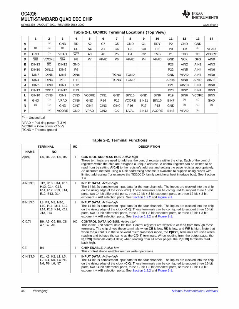
GC4016MULTI-STANDARD QUAD DDC CHIPSLWS133B–AUGUST 2001–REVISED JULY 2009 www.ti.com
Table 2-1. GC4016 Terminal Locations (Top View)1 2 3 4 5 6 7 8 9 10 11 12 13 14
A (1) GND RD A2 C7 C5 GND C1 RDY P2 GND GNDB (1) (1) (1) CE A4 A1 C6 C3 C0 P3 P0 TCK (1) VPADC GND (1) VPAD WR A3 A0 P5 C4 C2 TMS P1 TDO TDI VCORED SIB VCORE SIA P8 P7 VPAD P6 VPAD P4 VPAD GND SCK SFS AIN0E DIN13 SO DIN12 GND P23 AIN2 AIN1 AIN3F DIN10 DIN11 DIN9 P9 P22 AIN5 AIN4 AIN6G DIN7 DIN8 DIN5 DIN6 TGND TGND GND VPAD AIN7 AIN8H DIN4 DIN3 P10 P11 TGND TGND AIN10 AIN9 AIN12 AIN11J DIN2 DIN0 DIN1 P12 P21 AIN13 BIN1 BIN0K CIN13 CIN11 CIN12 P13 P20 BIN2 BIN4 BIN3L CIN10 CIN8 CIN9 CIN5 VCORE CIN1 GND BIN13 GND BIN9 P19 BIN6 VCORE BIN5M GND (1) VPAD CIN6 GND P14 P15 VCORE BIN11 BIN10 BIN7 (1) (1) GNDN (1) (1) GND CIN7 CIN4 CIN3 CIN0 P16 P17 P18 GND (1) (1) (1)
P (1) VCORE GND VPAD CIN2 CK DVAL BIN12 VCORE BIN8 VPAD (1)
(1) = Unused ballVPAD = Pad ring power (3.3 V)VCORE = Core power (2.5 V)TGND = Thermal ground
Table 2-2. Terminal FunctionsTERMINAL I/O DESCRIPTION
NAME NO.A[0:4] C6, B6, A5, C5, B5 I CONTROL ADDRESS BUS. Active-high
These terminals are used to address the control registers within the chip. Each of the controlregisters within the chip are assigned a unique address. A control register can be written to orread from by setting A[0:4] to the register's address and setting the page register appropriately.An alternate method using a 4 bit addressing scheme is available to support using buses withlimited addressing (for example the TI320C6X family peripheral host interface bus). See Section1.4.
AIN[13:0] J12, H13, H14, H11, I INPUT DATA, Active-highH12, G14, G13, The 14-bit 2s-complement input data for the four channels. The inputs are clocked into the chipF14, F12, F13, E14, on the rising edge of the clock (CK). These terminals can be configured to support three 16-bitE12, E13, D14 ports, two 14-bit differential ports, three 12-bit + 3-bit exponent ports, or three 12-bit + 3-bit
exponent + A/B selection ports. See Section 1.2.2 and Figure 2-1.BIN[13:0] L8, P9, M9, M10, I INPUT DATA, Active-high
L10, P11, M11, L12, The 14-bit 2s-complement input data for the four channels. The inputs are clocked into the chipL14, K13, K14, K12, on the rising edge of the clock (CK). These terminals can be configured to support three 16-bitJ13, J14 ports, two 14-bit differential ports, three 12-bit + 3-bit exponent ports, or three 12-bit + 3-bit
exponent + A/B selection ports. See Section 1.2.2 and Figure 2-1.C[0:7] B9, A9, C9, B8, C8, I/O CONTROL DATA I/O BUS. Active-high
A7, B7, A6 This is the 8-bit control data I/O bus. Control registers are written to or read from through theseterminals. The chip drives these terminals when CE is low, RD is low, and WR is high. Note thatwhen the output is in the wide-word microprocessor mode, the P[0:23] terminals are used whenreading and behave the same as the C[0:7] terminals. When reading from the output page, theP[0:23] terminals output data; when reading from all other pages, the P[0:23] terminals readback high.
CE B4 I CHIP ENABLE. Active-lowThis control strobe enables read or write operations.
CIN[13:0] K1, K3, K2, L1, L3, I INPUT DATA, Active-highL2, N4, M4, L4, N5, The 14-bit 2s-complement input data for the four channels. The inputs are clocked into the chipN6, P6, L6, N7 on the rising edge of the clock (CK). These terminals can be configured to support three 16-bit
ports, two 14-bit differential ports, three 12-bit + 3-bit exponent ports, or three 12-bit + 3-bitexponent + A/B selection ports. See Section 1.2.2 and Figure 2-1.
Packaging46 Submit Documentation Feedback

GC4016MULTI-STANDARD QUAD DDC CHIP
www.ti.com SLWS133B–AUGUST 2001–REVISED JULY 2009
Table 2-2. Terminal Functions (continued)TERMINAL I/O DESCRIPTION
NAME NO.CK P7 I INPUT CLOCK. Active-high
The clock input to the chip. The AIN, BIN, CIN, DIN, DVAL, SIA and SIB input signals areclocked into the chip on the rising edge of this clock. The SO, P, SFS, SCK and RDY outputs areclocked out on the rising edge of this clock.
DIN[13:0] E1, E3, F2, F1, F3, I INPUT DATA, Active-highG2, G1, G4, G3, H1, The 14-bit 2s-complement input data for the four channels. The inputs are clocked into the chipH2, J1, J3, J2 on the rising edge of the clock (CK). These terminals can be configured to support three 16-bit
ports, two 14-bit differential ports, three 12-bit + 3-bit exponent ports, or three 12-bit + 3-bitexponent + A/B selection ports. See Section 1.2.2 and Figure 2-1.
DVAL P8 I DATA VALID. Active-lowThis terminal is normally grounded. This terminal must be low to enable the internal clock. DVALis clocked into the chip on the rising edge of CK, and, if high, disables the following CK edge tothe channels and resampler. It does not affect the clock to the output circuitry. Because DVALenables or disables the internal clock, it can be used as a data enable for non-continuous inputdata. This terminal should never be held high for more than 1 ms. DVAL is used as a 2× clockinput when the CK_2X_EN control bit is high (see Section 1.2.9).
P[0:3] B11, C11, A11, B10 O BIT SERIAL AND NIBBLE OUTPUT DATA, Active-high, 3-stateThe nibble and bit serial output terminals. In the serial mode, these are individual outputs; in thenibble mode these form a 4-bit nibble (P0 is normally the LSB of the nibble; P3 is the MSB). Theoutput bits are clocked out coincident with the rising edge of SCK (falling edge if INV_SCK = 1).These terminals are in the high-impedance state at power up and are enabled by EN_P0,EN_P1, EN_P2 and EN_P3.
P[0:23] B11, C11, A11, B10, O PARALLEL OUTPUT DATA, Active-high, 3-stateD9, C7, D7, D5, D4, The 24-bit parallel output port. These output bits are clocked out by CK coincident with the risingF4, H3, H4, H5, H6, edge of SCK (falling edge if INV_SCK = 1) with the SFS and RDY terminals used to identify validM6, M7, N8, N9, data (see Section 1.2.8.6). These terminals are in the high-impedance state at power up and areN10, L11, K11, J11, enabled by the EN_PAR control register bit. These terminals can are used in the wide wordF11, E11 microprocessor mode. In this mode the terminals are used as part of the control bus when read
from the data output page (see Section 1.2.8).RD A4 I READ ENABLE. Active-low
The register selected by A[0:4] and the page register are output on the C[0:7] terminals whenRD and CE are low.
RDY A10 I/O READY FLAG, programmable active-high or -lowUsed to identify when new outputs are available in the serial, nibble, and microprocessor outputmodes. In the link mode, RDY is an input signal tied to the LACK output signal from SHARC DSPchips. In the parallel mode, it is a data-valid flag. The RDY signal is clocked out on the risingedge of CK. This terminal is in the high-impedance state at power up and is enabled by theEN_RDY control register bit.
SCK D12 O SERIAL DATA CLOCK, Active-high or -low, 3-stateThe serial, nibble, link, and parallel data-output clock. The SCK signal is clocked out on the risingedge of CK. The SFS, RDY, and P output signals are clocked out of the chip coincident with theactive edge of this clock. The active edge of the clock is user-programmable. This terminalplaced in the high-impedance state at power up and is enabled by the EN_SCK control registerbit.
SFS D13 O SERIAL FRAME STROBE, Active-high or -low, 3-stateThe bit serial word strobe. This strobe identifies the beginning of a frame, a complex pair, or aword within bit-serial output streams as controlled by the SFS_MODE control register bits. Thepolarity of this signal is user programmable. This terminal is put in the high-impedance state atpower up and is enabled by the EN_SFS control register bit. This terminal is also used as adata-valid signal for parallel outputs.
SIA, SIB D3, D1 I SYNC IN A and B. Active-lowThe sync inputs to the chip. All timers, accumulators, and control counters (except the resamplertime delay accumulator) are, or can be, synchronized to SIA or SIB. These syncs are clockedinto the chip on the rising edge of the input clock (CK).
SO E2 O SYNC OUT. Active-lowThis signal is either a delayed version of one of the input syncs SIA or SIB, the sync counter'sterminal count (TC), or a one-shot strobe. The SO signal is clocked out of the chip on the risingedge of the input clock (CK).
TCK, TDI, B12, C13, C10 I JTAG INTERFACE. Active-high input terminalsTMS The JTAG interface (See Section 1.2.15)TDO C12 O JTAG INTERFACE. 3-state output terminal
The JTAG interface (See Section 1.2.15)
Submit Documentation Feedback Packaging 47

GC4016MULTI-STANDARD QUAD DDC CHIPSLWS133B–AUGUST 2001–REVISED JULY 2009 www.ti.com
Table 2-2. Terminal Functions (continued)TERMINAL I/O DESCRIPTION
NAME NO.WR C4 I WRITE ENABLE. Active-low input terminal
The value on the C[0:7] terminals is written into the register selected by the A[0:4] and pageregister when WR and CE are low.
48 Packaging Submit Documentation Feedback

3 Control Registers
3.1 Global Controls
GC4016MULTI-STANDARD QUAD DDC CHIP
www.ti.com SLWS133B–AUGUST 2001–REVISED JULY 2009
The chip is configured by writing to eight bit-control registers. These registers are accessed for reading orwriting using the control bus terminals (CE, RD, WR, A[0:4], and C[0:7]) described in Section 1.4. The32-word address space is split into eight global registers (addresses 0–7), eight unused registers(addresses 8–15), and 16 paged registers (addresses 16–31). The global registers are available fromeach page. Address 2 is the page register, which selects the control registers that are accessed byaddresses 16 through 31.
The eight global control registers are shown in Table 3-1.
Table 3-1. Global Control RegistersADDRESS NAME DESCRIPTION
0 Global reset Miscellaneous general controls1 Status µP ready/missed, resampler overflows, checksum ready2 Page Page register for both 4- and 5-bit addressing modes3 Checksum Checksum results register4 General syncs Syncs for output, checksum. One shot.5 Count sync Sync for counter, ramp selection6 Counter byte 0 Ramp counter least-significant byte7 Counter byte 1 Ramp counter most-significant byte
ADDRESS 0: Global Reset, Powers up as 0xF0. Suggested default is 0xF8 during configuration, 0x08afterwards.
BIT TYPE NAME DESCRIPTION0 (LSB) R/W CK_LOSS_DETECT Disable the clock-loss detection circuitry. This circuitry protects the chip against a current
surge that may result if the clock is inactive for more than 100 ms. Setting this bit turns offthe clock-loss detection circuitry. Used for test, not recommended for general use.
1 R/W CK_2X_TEST Test mode to output the doubled clock on SO. DVAL must be low. Normally set to zero.2 R/W CK_2X_EN Changes the DVAL terminal to become a CK_2X input terminal. The chip normally uses an
internally generated doubled clock (twice the CK clock). Setting this bit allows an externallygenerated doubled clock to be used. Used in test, not recommended for general use.
3 R/W EDGE_WRITE Sets the edge write mode for the control interface. When low, the data must be stable whilethe write strobe is low. When high, the outputs are latched on the rising edge of the writestrobe (WR | CE). A short (approximately 15 ns) write recovery time is required, duringwhich the chip should not be read from or written to. Recommended to be set high.
4 R/W RESAMPLER_RESET This bit resets the resampler. This bit is set during power up and is cleared afterconfiguration.
5 R/W PAD_RESET Forces SFS and RDY pads to high-impedance state during power up. The user must clearthis bit for proper operation of SFS and RDY.
6 R/W OUT_BLK_RESET This bit resets the output formatter block. This bit is set during power up and is clearedafter configuration.
7 (MSB) R/W GLOBAL_RESET This bit powers down the chip and puts the output terminals in the high-impedance state.This bit is set during power up and is cleared after configuration.
ADDRESS 1: Status Register, Suggested default = 0x00
BIT TYPE NAME DESCRIPTION0 (LSB) R/W READY The user sets this bit after reading the output registers. The chip clears this bit when new
values have been loaded and it is time to read them.1 R/W MISSED The chip sets this bit If the user has not set the READY bit before the chip loads the output
registers. This bit high indicates that an error has occurred.2 R/W RES_IOV This control bit is set by the chip whenever the resampler I channel overflows. The user can
monitor this bit to see if the gain is too high. The user clears the bit by writing a zero to it.
Submit Documentation Feedback Control Registers 49

GC4016MULTI-STANDARD QUAD DDC CHIPSLWS133B–AUGUST 2001–REVISED JULY 2009 www.ti.com
BIT TYPE NAME DESCRIPTION3 R/W RES_QOV This control bit is set by the chip whenever the resampler Q channel overflows. The user
can monitor this bit to see if the gain is too high. The user clears the bit by writing a zero toit.
4 R/W CHECK_DONE This bit is set when the checksum sync is active (see DIAG_SYNC in address 4). The usercan count sync cycles by clearing this bit and then waiting for it to be set. The checksum iscomplete afterthis bit has been cleared and set four times.
5-7 (MSBs) R ZERO Reads back as zero.
The READY bit is used to tell an external processor when new output samples are ready to be read. Ifdesired, the RDY terminal can be used as an interrupt to the external processor (See Section 1.11.1) totell the processor when to read new samples. The user does not need to set the READY bit if RDY isused. If READY is not set, however, the MISSED flag is not valid.
ADDRESS 2: Page Register
BIT TYPE NAME DESCRIPTION0 (LSB) R/W A3 Used in the 4_BIT_ADDRESS mode (see global register 4) as address bit A3. This bit is
unused if 4_BIT_ADDRESS = 0.1–7 (MSBs) R/W PAGE[0:6] Page number for addressing different portions of the chip.
In normal mode, the LSB is unused. PAGE is decoded to select the different control pages (seeTable 3-2). Note that addresses 0–7 are globally visible regardless of the PAGE value. Addresses 8–15are unused. Addresses 16–31 are paged. In the 4-bit address mode, the LSB provides address bit A3,effectively reducing each page to eight words and doubling the number of pages.
ADDRESS 3: Checksum Register
BIT TYPE NAME DESCRIPTION0–7 R CHECKSUM[0:7] The checksum
The checksum register is a read-only register which contains the checksum of the output data. Thechecksum is stored in the checksum register and then starts over again each time the DIAG_SYNC (Seeaddress 4) occurs.
ADDRESS 4: General Sync Register, Suggested default = 0x27, cleared by power up
BIT TYPE NAME DESCRIPTION0–2 (LSBs) R/W DIAG_SYNC The checksum generator is strobed by this sync. See Table 1-7 for the possible sync
selections.3–5 R/W OUTPUT_SYNC The selected sync is inverted and output on the SO terminal. See Table 1-7.6 R/W 4_BIT_ADDRESS This mode allows four address bits (such as the expansion bus of the TI320C6202) instead
of 5 to be used. In this mode, each page contains eight words (rather than 16). The LSB ofthe page register is used as address bit A3. Terminal A3 should be grounded in this mode.
7 (MSB) R/W DIFF_IN Enables differential receivers. Both this bit and the corresponding bits in each channel mustbe set to receive differential signals properly. This bit should be cleared for other inputs andfor minimum power consumption.
ADDRESS 5: Count Sync Register, Suggested default = 0x50
BIT TYPE NAME DESCRIPTION0–1 (LSB) R/W DIAG_SOURCE This 2-bit field selects the diagnostic input source used when the INPUT_SEL field in each
channel’s control register is set to 6 or 7 (See channel control address 27). DIAG_SOURCE= 0 selects the 16 LSBs of the counter (see addresses 6 and 7) as a diagnostic ramp.DIAG_SOURCE = 1 is a zero input, DIAG_SOURCE = 2 is unused, DIAG_SOURCE = 3gives a 0x4000 constant input.
2–4 R/W COUNTER_SYNC Synchronizes the sync counter. This counter is used to generate the periodic TC sync. SeeTable 1-7.
5 R/W COUNT_TEST Used during factory tests. Should be set to 0 for normal operation.
Control Registers50 Submit Documentation Feedback
3.2 Paged Registers
3.3 CFIR Coefficient Pages
GC4016MULTI-STANDARD QUAD DDC CHIP
www.ti.com SLWS133B–AUGUST 2001–REVISED JULY 2009
BIT TYPE NAME DESCRIPTION6 R/W OS_MODE The ONE_SHOT signal is a level, not a pulse when this bit is set.7 (MSB) R/W ONE_SHOT The one-shot sync signal (OS) is generated when this bit is set. If OS_MODE is low, then a
one-shot pulse (one clock cycle wide) is generated. If OS_MODE is high, then theONE_SHOT sync is active while this bit is high. This bit must be cleared before anotherone-shot pulse can be generated.
ADDRESS 6: Counter Byte 0, Suggested default = DEC (CIC decimation value)
BIT TYPE NAME DESCRIPTION0–7 R/W CNT[0:7] The LSBs of the counter cycle period
ADDRESS 7: Counter Byte 1, Suggested default = DEC
BIT TYPE NAME DESCRIPTION0–7 R/W CNT[8:15] The 8 MSBs of the counter cycle period
The chip's internal sync counter counts in cycles of 256(CNT + 1) clocks. A terminal count signal (TC) isoutput at the end of each cycle. The counter can be synchronized to an external sync as specified in thecount sync register (address 5). If CNT is set so that 256(CNT + 1) is a multiple of 16 times the CICdecimation ratio (i.e., a multiple of 16N), then the terminal count of this counter can be output on the SOterminal and used to synchronize multiple GC4016 chips periodically.
Addresses 16 to 31 are used in pages as determined by the page map register (address 2).
Table 3-2. Page AssignmentsPAGE DESCRIPTION PAGE DESCRIPTION
0, 1 Channel-A CFIR coefficients 24, 25 Channel-D CFIR coefficients2–5 Channel-A PFIR coefficients 26–29 Channel-D PFIR coefficients6 Channel-A frequency 30 Channel-D frequency7 Channel-A control 31 Channel-D control8, 9 Channel-B CFIR coefficients 32–63 Resampler coefficients10–13 Channel-B PFIR coefficients 64 Resampler control14 Channel-B frequency 65 Resampler ratios15 Channel-B control 66–95 Unused16, 17 Channel-C CFIR coefficients 96, 97 Output data18–21 Channel-C PFIR coefficients 98 Output control22 Channel-C frequency 99–127 Unused23 Channel-C control
The following sections describe each of these pages.
The user-programmable filter CFIR coefficients are stored using pages 0 and 1 for channel A, pages 8and 9 for channel B, pages 16 and 17 for channel C, and pages 24 and 25 for channel D.
Table 3-3. CFIR Coefficient PagesPages 0, 8, 16, and 24 Pages 1, 9, 17, and 25
AddressDescription Description
16 h0 LSBs (end or first tap) h8 LSBs17 h0 MSBs (end or first tap) h8 MSBs18 h1 LSBs h9 LSBs
Submit Documentation Feedback Control Registers 51

3.4 PFIR Coefficient Pages
GC4016MULTI-STANDARD QUAD DDC CHIPSLWS133B–AUGUST 2001–REVISED JULY 2009 www.ti.com
Table 3-3. CFIR Coefficient Pages (continued)Pages 0, 8, 16, and 24 Pages 1, 9, 17, and 25
AddressDescription Description
19 h1 MSBs h9 MSBs20 h2 LSBs h10 LSBs (center tap)21 h2 MSBs h10 MSBs (center tap)22 h3 LSBs Unused23 h3 MSBs24 h4 LSBs25 h4 MSBs26 h5 LSBs27 h5 MSBs28 h6 LSBs29 h6 MSBs30 h7 LSBs31 h7 MSBs
Coefficient h0 is the first coefficient and coefficient h10 is the center coefficient of the filter's impulseresponse. The 16-bit 2s-complement coefficients are stored in 2 bytes, least-significant byte first; forexample, the LSBs of coefficient 0 are stored in address 16 and the MSBs in address 17.
TO LOAD A COEFFICIENT, THE USER MUST WRITE THE LSBYTE FIRST FOLLOWED BY THEMSBYTE. Unknown values are written into the LSBs if the MSB is written first. The coefficient registersare read/write.
The user-programmable filter PFIR coefficients are stored using pages 2, 3, 4, and 5 for channel A, pages10, 11, 12, and 13 for channel B, pages 18, 19, 20, and 21 for channel C, and pages 26, 27, 28, and 29for channel D.
Table 3-4. PFIR Coefficient PagesAddress Pages 2, 10, 18, and 26 Pages 3, 11, 19, and 27 Pages 4, 12, 20, and 28 Pages 5, 13, 21, and 29
Description Description Description Description16 h0 LSBs (end or first tap) h8 LSBs h16 LSBs h24 LSBs17 h0 MSBs (end or first tap) h8 MSBs h16 MSBs h24 MSBs18 h1 LSBs h9 LSBs h17 LSBs h25 LSBs19 h1 MSBs h9 MSBs h17 MSBs h25 MSBs20 h2 LSBs h10 LSBs h18 LSBs h26 LSBs21 h2 MSBs h10 MSBs h18 MSBs h26 MSBs22 h3 LSBs h11 LSBs h19 LSBs h27 LSBs23 h3 MSBs h11 MSBs h19 MSBs h27 MSBs24 h4 LSBs h12 LSBs h20 LSBs h28 LSBs25 h4 MSBs h12 MSBs h20 MSBs h28 MSBs26 h5 LSBs h13 LSBs h21 LSBs h29 LSBs27 h5 MSBs h13 MSBs h21 MSBs h29 MSBs28 h6 LSBs h14 LSBs h22 LSBs h30 LSBs29 h6 MSBs h14 MSBs h22 MSBs h30 MSBs30 h7 LSBs h15 LSBs h23 LSBs h31 LSBs (center tap)31 h7 MSBs h15 MSBs h23 MSBs h31 MSBs (center tap)
Control Registers52 Submit Documentation Feedback

3.5 Channel Frequency Pages
3.6 Channel Control Pages
GC4016MULTI-STANDARD QUAD DDC CHIP
www.ti.com SLWS133B–AUGUST 2001–REVISED JULY 2009
Coefficient h0 is the first coefficient and coefficient h31 is the center coefficient of the filter's impulseresponse. The 16-bit 2s-complement coefficients are stored in 2 bytes, least-significant byte first; forexample, the LSBs of coefficient 0 are stored in address 16 and the MSBs in address 17.
TO LOAD A COEFFICIENT, THE USER MUST WRITE THE LSBYTE FIRST FOLLOWED BY THEMSBYTE. Unknown values are written into the LSB if the MSB is written first. The coefficient registers areread/write.
Pages 6, 14, 22, and 30 contain the phase and frequency control settings for the four channels. Thefrequency and phase for channel A are set in page 6. The frequency and phase for channel B are set inpage 146. The frequency and phase for channel C are set in page 22. The frequency and phase forchannel D are set in page 30. All registers are read/write.
ADDRESSES 16, 17: Phase
ADDRESS TYPE NAME DESCRIPTION16 R/W PHASE[0:7] Byte 0 (LSBs) of PHASE17 R/W PHASE[8:15] Byte 1 (MSBs) of PHASE
The 16-bit phase offset is defined as:PHASE = 216P/2π
where P is the desired phase in radians, from 0 to 2π.
ADDRESSES 18, 19, 20, and 21: Frequency
ADDRESS TYPE NAME DESCRIPTION18 R/W FREQ[0:7] Byte 0 (LSBs) of FREQ19 R/W FREQ[8:15] Byte 1 of FREQ20 R/W FREQ[16:23] Byte 2 of FREQ21 R/W FREQ[24:31] Byte 3 (MSBs) of FREQ
The 32-bit frequency control word is defined as:FREQ = 232f/fCK
where f is the desired tuning frequency and fCK is the chip clock rate (CK). Use positive frequency valuesto downconvert signals. Use negative frequency values to invert the signal spectrum. The 32-bit2s-complement frequency words are entered as four bytes, the least-significant byte in the lowest address,the most-significant in the highest address.
These pages contain the various control settings for the four channels. To configure channels A, B, C, andD, use pages 7, 15, 23, and 31, respectively. All registers are read/write. Table 3-5 summarizes theregisters.
Table 3-5. Channel Control RegistersADDRESS NAME DESCRIPTION
16 Channel reset Resets the channel and sets SHIFT17 Frequency sync Phase and frequency syncs18 NCO sync NCO and dither syncs19 Blank Blank controls20 Dec sync Synchronizes CIC decimation and flush21, 22 Decimation ratio Sets CIC decimation and sync for fine gain23 CIC scale Sets CIC gain and MIX20B
Submit Documentation Feedback Control Registers 53
GC4016MULTI-STANDARD QUAD DDC CHIPSLWS133B–AUGUST 2001–REVISED JULY 2009 www.ti.com
Table 3-5. Channel Control Registers (continued)ADDRESS NAME DESCRIPTION
24 SplitIQ SplitIQ and negate control25 CFIR Quarter delays, Coarse, Nosym126 PFIR Half delays, Nosym227 Input Selects input format and port28 Peak control Controls peak and overflow detection counter29 Peak read Number of peaks (overflows) during last sync period30, 31 Fine gain Fine-gain control
ADDRESS 16: Channel Reset Set to 0x80 on power up, Suggested default = 0x0C
BIT TYPE NAME DESCRIPTION0–2 (LSBs) R/W SHIFT Value used to shift up the mixer output if USE_SHIFT is high. Note that if USE_SHIFT is
high and MIX20B is set, then SHIFT is restricted to the range of 4–7.3 R/W USE_SHIFT Selects SHIFT if high. If low, the mixer output shift value is provided by the exponent bits of
the floating point input format (see Section 1.2.2).4–6 R/W — Unused7 (MSB) R/W CH_RESET This bit resets the channel. If high, the channel is in a reset state with the clock disabled.
ADDRESS 17: Frequency Sync, Suggested default = 0x77
BIT TYPE NAME DESCRIPTION0–2 (LSB) R/W PHASE_SYNC The new phase offset takes effect on this sync.3 R/W — Unused4–6 R/W FREQ_SYNC The new frequency setting takes effect on this sync.7 (MSB) R/W — Unused
These syncs use the selections shown in Table 1-7.
The FREQ_SYNC and PHASE_SYNC are typically set to be always so that frequency and phase settingstake effect immediately as they are written into their control registers. Due to the asynchronous nature ofthe interface in this mode, a few samples are mixed with transient frequencies until the new frequency andphase values are established. If these transients are undesirable OR if the accumulated phase must becontrolled, then another sync source should be used.
ADDRESS 18: NCO Sync, Suggested default = 0x22
BIT TYPE NAME DESCRIPTION0-2 (LSB) R/W NCO_SYNC The NCO is initialized to the phase setting by this sync.3 R/W — Unused4–6 R/W DITHER_SYNC The dither circuit is reset to zero by this sync.7 (MSB) R/W — Unused
These syncs use the selections shown in Table 1-7.
The NCO_SYNC can be changed to SIB so that the SIB sync can be used to synchronize the NCOphases of multiple channels or chips.
The DITHER_SYNC is used to turn on or off the dithering of the NCO phase. Dithering is turned on bysetting DITHER_SYNC to never. Dithering is turned off by setting DITHER_SYNC to always, whichcauses it to remain reset to zero.
During diagnostics, the NCO_SYNC and DITHER_SYNC should be set to TC (5).
If the user wishes to allow the chip to free-run, asynchronous to other chips, then these sync settings canbe set to never.
Control Registers54 Submit Documentation Feedback

GC4016MULTI-STANDARD QUAD DDC CHIP
www.ti.com SLWS133B–AUGUST 2001–REVISED JULY 2009
ADDRESS 19: Zero-Pad Mode-Control Register, Suggested default = 0x20
BIT TYPE NAME DESCRIPTION0–3 (LSBs) R/W NZEROS The number of zeroes to insert between each sample in the blank mode. Ranges from 0
to 15. Note that this introduces a gain of 1/(NZEROS + 1).4–6 R/W ZPAD_SYNC The sync selection from Table 1-7 for the zero-pad function (see Figure 1-5).7 (MSB) R/W ZPAD_EN Turn on zero-padding for this channel.
ADDRESS 20: Dec and Flush Sync Register, Suggested default = 0x22
BIT TYPE NAME DESCRIPTION0–2 (LSBs) R/W DEC_SYNC Synchronizes the decimation control counter. The decimation counter controls the filtering
of each channel.3 R/W — Unused4–6 R/W FLUSH_SYNC Synchronizes the flush sync for this channel.7 (MSB) R/W — Unused
The decimation counter sync (DEC_SYNC) may be periodic without interrupting processing so long as thesync period is a multiple of 8N. A decimation sync should be issued if the decimation control is changed.
Each channel should be flushed (FLUSH_SYNC) when the chip is being initialized or when the decimationcontrol is changed. The flush lasts for 24N clocks after the sync occurs. The channel flush syncs normallyare left in a never mode. During diagnostics, the channels must be flushed at the beginning of each synccycle.
The user may wish to flush a channel when a new frequency is selected in order to purge the datapath ofthe last signal.
ADDRESS 21: Decimation Ratio Byte 0, Suggested default = 0x07
BIT TYPE NAME DESCRIPTION0–7 R/W DEC[0:7] The LSBs of the decimation control
ADDRESS 22: Decimation Ratio Byte 1, Suggested default = 0x70
BIT TYPE NAME DESCRIPTION0–3 (LSBs) R/W DEC[8:11] The 4 MSBs of the decimation control4-6 R/W GAIN_SYNC The new fine gain takes effect on this sync.7 (MSB) R/W — Unused
The CIC decimation is N. When processing in normal mode (not SPLITIQ), DEC should be set to N – 1,where N ranges from 8 to 4096. When processing in SPLITIQ mode, DEC should be set to 2N – 1, whereN ranges from 4 to 2048.
ADDRESS 23: CIC Scale, Suggested default = 0x79
BIT TYPE NAME DESCRIPTION0–2 (LSBs) R/W SCALE SCALE ranges from 0 to 5.3–5 R/W BIG_SCALE BIG_SCALE ranges from 0 to 7.6 R/W MIX20B Round mixer output to 20 bits if MIX20B = 1 or to 16 bits if MIX20B = 0. If MIX20B = 1, then
SHIFT (see address 16) must be at least 4 to shift the extra 4 bottom bits into the datapath.For very large decimations (>3104), unity gain through the CIC can only be accomplishedby using a smaller SHIFT, and hence MIX20B must be zero. The default is MIX20B = 1.
7 (MSB) R/W — Unused
Submit Documentation Feedback Control Registers 55

GC4016MULTI-STANDARD QUAD DDC CHIPSLWS133B–AUGUST 2001–REVISED JULY 2009 www.ti.com
The CIC filter has a gain which is equal to N5. To remove this gain, the CIC inputs are prescaled down by(62 – SHIFT – SCALE – 6 × BIG_SCALE) bits before filtering. The values of SHIFT, SCALE, andBIG_SCALE must be such that:
SHIFT + SCALE + 6 × BIG_SCALE) ≤ (62 – 5log2N + log2(NZERO + 1))
Overflows due to improper gain settings go undetected if this relationship is violated. For example, thisrestriction means that for N equal to 8, and SHIFT equal to 4, BIG_SCALE and SCALE should be lessthan or equal to 7 and 1, respectively.
ADDRESS 24: SplitIQ, Suggested default = 0x00
BIT TYPE NAME DESCRIPTION0–3 (LSBs) R/W NEG_CTL A 4-bit pattern that multiplies the output of the PFIR by ±1. This is used to perform
complex-to-real conversion (fS/4 upconvert), flip the spectrum, or perform an fS/2 frequencyshift.
4 R/W SPLITIQ Process only the real data (at twice the throughput). Used to allow two channels to beganged together for wider output bandwidth.
5 R/W IONLY All samples output by this channel are real. Used in the SPLITIQ mode to identify thechannel generating the I-half of the complex output.
6 R/W QONLY All samples output by this channel are imaginary. Used in the SPLITIQ mode to identify thechannel generating the Q-halfof the complex output. When performing complex-to-real conversion, this bit must be set(among others).
7 (MSB) R/W — Unused
Section 1.2.3 and Section 1.2.4 describe how to use these controls.
ADDRESS 25: CFIR, Suggested default = 0x00
BIT TYPE NAME DESCRIPTION0 (LSB) R/W NO_SYM_CFIR When this bit is high, CFIR is an 11-tap asymmetric filter. Coefficient h0 is multiplied by the
newest data.1 R/W QDLY_CFIR Delay the Q sample stream by one CFIR input sample. Effectively, this is a 1/4-sample
delay of the output PFIR. Used in the multichannel modes (see Section 1.2.4).2 R/W IDLY_CFIR Delay the I-sample stream by one CFIR input sample. Effectively, this is a 1/4-sample delay
of the output PFIR. Used in the multichannel modes (see Section 1.2.4).3 R/W — Unused4–-6 R/W COARSE This introduces a gain of 2COARSE after the CIC but before rounding to 20 bits to feed CFIR.
This allows optimization of gain in applications where it is known that most of the signalenergy presented to the A/D has been filtered out by the CIC. An example of such anapplication is an FDM stack.
7 (MSB) R/W TEST Test mode. Should be set to 0.
ADDRESS 26: PFIR, Suggested default = 0x00
BIT TYPE NAME DESCRIPTION0 (LSB) R/W NO_SYM_PFIR When this bit is high, the PFIR is a 32-tap asymmetric filter. Coefficient h0 is multiplied by
the newest data.1 R/W QDLY_PFIR Delay the Q sample stream by one PFIR input sample. Effectively, this is a 1/2-sample
delay of the output PFIR. Used in the real or multichannel modes (see Section 1.2.3 andSection 1.2.4).
2 R/W IDLY_PFIR Delay the I-sample stream by one PFIR input sample. Effectively, this is a 1/2-sample delayof the output PFIR.Used in the real or multichannel modes (see Section 1.2.3 andSection 1.2.4).
3–4 R/W PEAK_SELECT Select the overflow detection source for the peak counter. Only used if PEAK_MODE = 1.Selects CFIR, COARSE_GAIN, or PFIR for values 0, 1, or 2, respectively (the values 2 and3 are the same). See address 28.
5–7 (MSBs) R/W — Unused
Control Registers56 Submit Documentation Feedback

3.7 Resampler Coefficient Pages (Pages 32–63)
GC4016MULTI-STANDARD QUAD DDC CHIP
www.ti.com SLWS133B–AUGUST 2001–REVISED JULY 2009
ADDRESS 27: Input, Suggested default = 0x00
BIT TYPE NAME DESCRIPTION0–2 (LSBs) R/W INPUT_SEL Selects which input port to use for this channel. Values 0–3 select inputs A–D, respectively.
Values 4 and 5 select differential inputs A and B. Values 6 and 7 select the internaldiagnostic source (see general address 5). Note that for differential inputs, one must alsoenable the differential receivers by setting the DIFF_IN bit in register 4.
3 R/W SEL_AB Selects the A/B channel in the dual 12-bit-plus-exponent mode (INPUT_MODE = 3). IfSEL_AB is 0, then the samples with their A/B flag low are used. If SEL_AB is high, then thesamples with their A/B flag high are used.
4–5 R/W INPUT_MODE Selects the input format: 0 is the 14-bit input mode, 1 is the 16-bit input mode, 2 is the12-bit-plus-exponent mode, and 3 is the dual 12-bit-plus-exponent mode.
6 R/W — Unused7 (MSB) R/W MSB_POL Invert the MSB polarity. This converts an offset-binary-formatted input to 2s-complement
format.
ADDRESS 28: Peak Control, Suggested default = 0x1D
BIT TYPE NAME DESCRIPTION0–2 (LSBs) R/W PEAK_SYNC Synchronizes the peak-counter circuitry using the mode selected in Table 1-7. When the
peak sync occurs, the peak count is transferred to the read-only control register, and thepeak counter is cleared.
3–4 R/W PEAK_THRESHOLD When the input peak-detect mode is selected (PEAK_MODE = 0), the input word ischecked against a threshold. The threshold values are 1/4, 1/2, 3/4, or 4/4 (full scale) forPEAK_THRESH = 0, 1, 2, or 3, respectively. The absolute value of the top 11 bits iscompared to the selected threshold. This is only used when PEAK_MODE is zero.
5 R/W PEAK_MODE If PEAK_MODE is zero, the input word is selected as the source to the peak counter;otherwise, one of three overflow bits (see PEAK_SELECT at address 26) is monitored bythe peak counter.
6–7 (MSBs) R/W — Unused
ADDRESS 29: Peak Count, Read-only
BIT TYPE NAME DESCRIPTION0–7 R PEAK_COUNT Count of number of overflows or samples above threshold during last sync period. The
counter hard-limits at 255.
ADDRESS 30: Fine-Gain Byte 0, Suggested default = 0x00
BIT TYPE NAME DESCRIPTION0–7 R/W FINE_GAIN[0:7] The LSBs of the fine-gain control
ADDRESS 31: Fine-Gain Byte 1, Suggested default = 0x00
BIT TYPE NAME DESCRIPTION0–5 (LSBs) R/W FINE_GAIN[8:13] The MSBs of the fine-gain control6–7 (MSBs) R/W — Unused
The fine-gain control can apply a gain of FINE_GAIN/1024, providing a range of 0 to almost 16. Doublebuffering and synchronization for data transfer is provided to allow the user to change the gaindynamically without causing glitches in the signal (See GAIN_SYNC in address 22). This also allows theuser to change gain synchronously in multiple channels, even across different chips.
These pages store the 256 resampler coefficients. Storing resampler coefficient values is similar to storingthe coefficients for the CFIR and PFIR filters. The resampler coefficients are 12 bits with the 8 LSBswritten in one address, and the upper 4 bits written as the 4 LSBs of the next address. When reading backresampler coefficients, the top four bits of the second address always read back zero.
Submit Documentation Feedback Control Registers 57

GC4016MULTI-STANDARD QUAD DDC CHIPSLWS133B–AUGUST 2001–REVISED JULY 2009 www.ti.com
The resampler coefficient RAM must be written in blocks of eight addresses (four coefficients). Writes tothe RAM occur when a write is done to addresses 23 or 31. Supplying coefficients in sequential orderwrites correctly to the RAM. If just a portion of the resampler coefficient RAM is to be updated, then onemust write in blocks of the eight addresses 16 to 23, or 24 to 31. Writing to less than eight addressesresults either in no change to the RAM or in unknown changes to some coefficients.
TO LOAD A COEFFICIENT, THE USER MUST WRITE IN BLOCKS OF FOUR COEFFICIENTS. ONEMUST WRITE TO ADDRESSES 16–22, THEN ADDRESS 23, OR TO ADDRESSES 24–30, THENADDRESS 31.
Table 3-6 shows the coefficient register assignments when there is a single filter (NF = 0). For two filters(NF = 1), the two filters are interleaved, i.e., the heven in Table 3-6 contains one filter and hodd contains theother. For four filters (NF = 3), the four filters are interleaved, i.e., h0, h4, h8, ... is the first filter, h1, h5, h9,... is the second, etc.
Table 3-6. Resampler Coefficient Pages (Single-Filter Mode)Page
Address32 33 34 35 36 37 38 39 40 41 42 43 44 45 46 47
16 h0 h8 h16 h24 h32 h40 h48 h56 h64 h72 h80 h88 h96 h104 h112 h120
17 h0 h8 h16 h24 h32 h40 h48 h56 h64 h72 h80 h88 h96 h104 h112 h120
18 h1 h9 h17 h25 h33 h41 h49 h57 h65 h73 h81 h89 h97 h105 h113 h121
19 h1 h9 h17 h25 h33 h41 h49 h57 h65 h73 h81 h89 h97 h105 h113 h121
20 h2 h10 h18 h26 h34 h42 h50 h58 h66 h74 h82 h90 h98 h106 h114 h122
21 h2 h10 h18 h26 h34 h42 h50 h58 h66 h74 h82 h90 h98 h106 h114 h122
22 h3 h11 h19 h27 h35 h43 h51 h59 h67 h75 h83 h91 h99 h107 h115 h123
23 h3 h11 h19 h27 h35 h43 h51 h59 h67 h75 h83 h91 h99 h107 h115 h123
24 h4 h12 h20 h28 h36 h44 h52 h60 h68 h76 h84 h92 h100 h108 h116 h124
25 h4 h12 h20 h28 h36 h44 h52 h60 h68 h76 h84 h92 h100 h108 h116 h124
26 h5 h13 h21 h29 h37 h45 h53 h61 h69 h77 h85 h93 h101 h109 h117 h125
27 h5 h13 h21 h29 h37 h46 h53 h61 h69 h77 h85 h93 h101 h109 h117 h125
28 h6 h14 h22 h30 h38 h46 h54 h62 h70 h78 h86 h94 h102 h110 h118 h126
29 h6 h14 h22 h30 h38 h46 h54 h62 h70 h78 h86 h94 h102 h110 h118 h126
30 h7 h15 h23 h31 h39 h47 h55 h63 h71 h79 h87 h95 h103 h111 h119 h127
31 h7 h15 h23 h31 h39 h47 h55 h63 h71 h79 h87 h95 h103 h111 h119 h127
PageAddress
48 49 50 51 52 53 54 55 56 57 58 59 60 61 62 6316 h128 h136 h144 h152 h160 h168 h176 h184 h192 h200 h208 h216 h224 h232 h240 h248
17 h128 h136 h144 h152 h160 h168 h176 h184 h192 h200 h208 h216 h224 h232 h240 h248
18 h129 h137 h145 h153 h161 h169 h177 h185 h193 h201 h209 h217 h225 h233 h241 h249
19 h129 h137 h145 h153 h161 h169 h177 h185 h193 h201 h209 h217 h225 h233 h241 h249
20 h130 h138 h146 h154 h162 h170 h178 h186 h194 h202 h210 h218 h226 h234 h242 h250
21 h130 h138 h146 h154 h162 h170 h178 h186 h194 h202 h210 h218 h226 h234 h242 h250
22 h131 h139 h147 h155 h163 h171 h179 h187 h195 h203 h211 h219 h227 h235 h243 h251
23 h131 h139 h147 h155 h163 h171 h179 h187 h195 h203 h211 h219 h227 h235 h243 h251
24 h132 h140 h148 h156 h164 h172 h180 h188 h196 h204 h212 h220 h228 h236 h244 h252
25 h132 h140 h148 h156 h164 h172 h180 h188 h196 h204 h212 h220 h228 h236 h244 h252
26 h133 h141 h149 h157 h165 h173 h181 h189 h197 h205 h213 h221 h229 h237 h245 h253
27 h133 h141 h149 h157 h165 h173 h181 h189 h197 h205 h213 h221 h229 h237 h245 h253
28 h134 h142 h150 h158 h166 h174 h182 h190 h198 h206 h214 h222 h230 h238 h246 h254
29 h134 h142 h150 h158 h166 h174 h182 h190 h198 h206 h214 h222 h230 h238 h246 h254
30 h135 h143 h151 h159 h167 h175 h183 h191 h199 h207 h215 h223 h231 h239 h247 h255
Control Registers58 Submit Documentation Feedback

3.8 Resampler Control Page (Page 64)
GC4016MULTI-STANDARD QUAD DDC CHIP
www.ti.com SLWS133B–AUGUST 2001–REVISED JULY 2009
Table 3-6. Resampler Coefficient Pages (Single-Filter Mode) (continued)31 h135 h143 h151 h159 h167 h175 h183 h191 h199 h207 h215 h223 h231 h239 h247 h255
This page controls the resampler. The address assignments are:
Table 3-7. Resampler Control RegistersADDRESS NAME DESCRIPTION
16 N-channels Sets the number of channels and filters17 N-multiplies Sets the number of multiplies per output18 Filter select Maps channels to filter sets19 Final shift Sets the final gain shift20 Channel map Maps channels to outputs21 Add to Adds channel outputs together22 Clock divide Divides the clock to the resampler23 Ratio map Maps ratios to output channels24–31 — Unused
ADDRESS 16: N-Channels Out Register Suggested default = 0x23
BIT TYPE NAME DESCRIPTION0–1 (LSBs) R/W NC Must be set to NC = NCHAN – 1, where NCHAN is the number of output channels to be
generated. A value of NC = 0 means one output channel. A value of NC = 1 means twooutput channels. Use a value of NC = 3 for either three or four output channels. A value of2 produces erroneous results.
2–3 R/W NF Must be set to NF = NFILTER – 1, where NFILTER is the number of resampler filters. Usedto partition the resampler coefficient RAM. A value of NF = 0 means one filter (normalcase). A value of NF = 1 means two filters. A value of NF = 3 means four filters. A value of2 produces erroneous results.
4–6 R/W RES_SYNC The resampler is synchronized to this sync source (See Table 1-7). Resets the delayaccumulators in all channels at the same time.
7 (MSB) R/W — Unused
ADDRESS 17: N-Multiplies Register, Suggested default = 0x0E
BIT TYPE NAME DESCRIPTION0–5 (LSBs) R/W NM Must be set to NM = NMULT – 1, where NMULT is the number of resampler multiplies. The
minimum allowedvalue is NM = 5, the maximum is NM = 63, but typically the maximum is determinedby other constraints (see Section 1.2.5). In the case of a single-channel output theminimum value is NM = 6.
6 R/W NO_SYM_RES The resampler filter is presumed to be symmetric unless this bit is set.7 (MSB) R/W — Unused
ADDRESS 18: Filter Select Register, Suggested default = 0x00
BIT TYPE NAME DESCRIPTION0–1 (LSBs) R/W FILTER_SEL_0 The filter map for output channel 0. This selects which of the NFILTER filters to use for this
channel. Must be less than or equal to NFILTER.2–3 R/W FILTER_SEL_1 The filter map for output channel 14–5 R/W FILTER_SEL_2 The filter map for output channel 26–7 (MSB) R/W FILTER_SEL_3 The filter map for output channel 3
Submit Documentation Feedback Control Registers 59

GC4016MULTI-STANDARD QUAD DDC CHIPSLWS133B–AUGUST 2001–REVISED JULY 2009 www.ti.com
ADDRESS 19: Final Shift Register, Suggested default = 0x34
BIT TYPE NAME DESCRIPTION0–3 (LSBs) R/W FINAL_SHIFT The final shift up applied to all output channels before rounding and outputting. Valid
values are 0–15.4–5 R/W ROUND Round the output to 12 bits (ROUND = 0), 16 bits (ROUND = 1), 20 bits (ROUND = 2) or
24 bits (ROUND = 3). Note that the data is output from the resampler in all cases as 24-bitwords. Rounding is into the MSBs, unused LSBs of the 24-bit output words are not cleared.The chip’s output word size is set by BITS_PER_WORD in the output page, not byROUND.
6 R/W TAG_22 2-bit tag mode. Replaces the 2 LSBs of the 24-bit resampler output word with the 2 LSBs ofthe tag words. Changes the 24-bit round mode (ROUND = 3), if it used, to be a 22-bitround mode.
7 (MSB) R/W — Unused
ADDRESS 20: Channel Map Register, Suggested default = 0xE4
BIT TYPE NAME DESCRIPTION0–1 (LSBs) R/W CHAN_MAP_A The channel map for channel A. This tells the hardware which output channel the results of
downconverter channel A should be directed to.2–3 R/W CHAN_MAP_B The channel map for downconverter channel B.4–5 R/W CHAN_MAP_C The channel map for downconverter channel C.6–7 (MSBs) R/W CHAN_MAP_D The channel map for downconverter channel D.
This register maps downconverter channels to output (resampler) channels. For most applications, this isa simple map of channel A to output channel 0, channel B to output channel 1, etc. However, formultichannel modes (see Section 1.2.4) such as SPLITIQ, two or even four channels may be directed tothe same output channel.
ADDRESS 21: Add-To Register, Suggested default = 0x70
BIT TYPE NAME DESCRIPTION0 (LSB) R/W ADD_A_TO_B Add downconverter channel A to downconverter channel B.1 R/W ADD_B_TO_C Add downconverter channel B to downconverter channel C.2 R/W ADD_C_TO_D Add downconverter channel C to downconverter channel D.3 R/W ADD_D_TO_NEXT_A Not useful. Must be set to zero.4–6 R/W RATIO_SYNC Changes to the ratio map (address 23) are synchronized to this sync source.7 (MSB) R/W — Unused
When processing complex input signals, partial results are computed in adjacent channels that must besummed together to produce a meaningful result. This control bit informs the resampler to save the datapresented to its input and add it to the next sample presented (if the chip is properly set up, this is fromthe next channel). In this manner, the real and imaginary portions of the input are rejoined prior toresampling.
ADDRESS 22: Resampler Clock-Divide Register, Suggested default = 0x00
BIT TYPE NAME DESCRIPTION0–7 R/W RES_CLK_DIV Resampler clock division
In many applications, only a small portion of the resampler computational throughput is required. Powercan be reduced by dividing the clock that drives the resampler. The resampler clock rate is 2 × fCK/(1 +RES_CLK_DIV). Caution must be used to avoid dividing the clock so far that there are not enough clockcycles to complete the computations (see Section 1.2.5). It is recommended that an application first bebrought up without resampler clock division.
ADDRESS 23: Ratio Map Register, Suggested default = 0x00
Control Registers60 Submit Documentation Feedback

3.9 Resampler Ratio Page (Page 65)
3.10 Channel Output Pages (Pages 96 and 97)
3.11 Output Control Page (Page 98)
GC4016MULTI-STANDARD QUAD DDC CHIP
www.ti.com SLWS133B–AUGUST 2001–REVISED JULY 2009
BIT TYPE NAME DESCRIPTION0–1 (LSBs) R/W RATIO_MAP_0 The ratio map for channel 0. This tells the hardware which resampler ratio should be used
for output channel 0.2–3 R/W RATIO_MAP_1 The ratio map for output channel 1.4–5 R/W RATIO_MAP_2 The ratio map for output channel 2.6–7 (MSBs) R/W RATIO_MAP_3 The ratio map for output channel 3.
The default ratio maps select ratio 0 for output 0, ratio 1 for output 1, ratio 2 for output 2, and ratio 3 foroutput 3. The ratio maps can also be used to switch synchronously between resampling ratios. This allowsthe chip resampler to be used in timing loops where the ratio must toggle among several values whichhave been programmed into the chip.
This page stores four resampler ratios to be used by the resampler channels. Each ratio is a 32-bit ratio ofthe input sample rate to the output sample rate, with an implicit binary pointsix bits down from the top. The total range for the ratio is then 0 to 63. The hardware limits the decimationto be less than 32 (hence, the MSB of the 32-bit word should always be zero).
Table 3-8. Resampler Ratio PageADDRESS NAME ADDRESS NAME
16 RATIO_0 (LSBs) 24 RATIO_2 (LSBs)17 RATIO_0 25 RATIO_218 RATIO_0 26 RATIO_219 RATIO_0 (MSBs) 27 RATIO_2 (MSBs)20 RATIO_1 (LSBs) 28 RATIO_3 (LSBs)21 RATIO_1 29 RATIO_322 RATIO_1 30 RATIO_323 RATIO_1 (MSBs) 31 RATIO_3 (MSBs)
Addresses 16 through 31 on these pages are used to read output values. The outputs are 24-bit2s-complement numbers, which are read as three 8-bit bytes. Reading address 16 outputs 0 on C[0:7].Reading address 17 outputs the least-significant byte. Address 18 provides the middle byte. Address 19provides the most-significant byte. If microprocessor mode is enabled and terminals P[0:23] are enabled(by setting EN_P[0:3], EN_PAR), the full 24-bit word is simultaneously output P[0:23]. These are allread-only registers.
See Table 1-4, Table 1-5, and Table 1-6 for the data order in these pages.
This page controls the output. The following table summarizes the registers.
Table 3-9. Output Control RegistersADDRESS NAME DESCRIPTION
16 3-state controls Enables serial and parallel ports and controls17 Output format Sync output. Invert SCK, SFS, and RDY. Set RDY width. Enable tags.18 Output mode Select serial, nibble, parallel, or µP output. Select real or complex output. Enable nibble
reverse.19 Output frame control Select output frame length. Control SFS behavior.20 Output word sizes Select output word size, output block size, and words per frame.21 Output clock control Set clock divider for serial clock. Set number of active serial outputs.
Submit Documentation Feedback Control Registers 61

GC4016MULTI-STANDARD QUAD DDC CHIPSLWS133B–AUGUST 2001–REVISED JULY 2009 www.ti.com
Table 3-9. Output Control Registers (continued)ADDRESS NAME DESCRIPTION
22 Serial mux control Route serial streams to serial ports.23 Output tag A Tags for outputs AI and AQ24 Output tag B Tags for outputs BI and BQ25 Output tag C Tags for outputs CI and CQ26 Output tag D Tags for outputs DI and DQ27 Mask revision Reads back the chip’s mask revision number28 Miscellaneous Output enable for SO, four-frame strobe mode control
ADDRESS 16: 3-State Controls Cleared on power up, Suggested default = (see Table 1-3)
BIT TYPE NAME DESCRIPTION0 (LSB) R/W EN_SCK Enable SCK output. Used in serial, nibble, link, and parallel modes.1 R/W EN_RDY Enable RDY output. Used for parallel and microprocessor modes. RDY should be enabled
for the master chip in serial or nibble TDM mode. RDY should not be enabled for slavechips, or for the link mode.
2 R/W EN_SFS Enable SFS output. Used in serial, nibble, and parallel modes. Can be used as an interruptin link mode.
3 R/W EN_P0 Enable P0. Required for serial mode when outputting on P0, link, or nibble modes,wide-word microprocessor, and parallel modes.
4 R/W EN_P1 Enable P1. Required for serial mode when outputting on P1, link, or nibble modes, wideword microprocessor, and parallel modes.
5 R/W EN_P2 Enable P2. Required for serial mode when outputting on P2, link or nibble modes, wideword microprocessor, and parallel modes.
6 R/W EN_P3 Enable P3. Required for serial mode when outputting on P3, link or nibble modes, wideword microprocessor, and parallel modes.
7 (MSB) R/W EN_PAR Enable P4–P23. Used for parallel output and wide-word microprocessor modes.
All outputs except SO and the control port (C0–C7) power up in a high-impedance state and remain thatway until they are enabled. The control port (C0–C7) is high-impedance until both CE and RD are low andWR is high.
ADDRESS 17: Output Format, Suggested default = 0x40
BIT TYPE NAME DESCRIPTION0 (LSB) R/W INV_SCK Invert SCK output. The serial, nibble, link, and parallel outputs normally change on the
rising edge of SCK. If INV_SCK is set high, the clock is inverted, so data changes on thefalling edge.
1 R/W INV_RDY Invert RDY output. RDY is normally active-high. This control bit is used for microprocessorand parallel modes. It has no effect in serial, link, or nibble modes.
2 R/W INV_SFS Invert SFS output. SFS is normally active-high.3 R/W TAG_EN Enable tags. The 4-bit tags
replace the 4 LSBs of the data when TAG_EN is set. The BITS_PER_WORD (address 20)control determines the tag location.
4 R/W RDY_WIDTH The RDY pulse is 4 (RDY_WIDTH = 0) or 16 (RDY_WIDTH = 1) CK cycles. Valid for themicroprocessor mode only, must be set to 0 for all other modes.
5–7 (MSBs) R/W OUT_BLK_SYNC Output circuit sync source. See Table 1-7 for the sync modes.The OUT_BLK_SYNC is used to synchronize the output timing among multiple GC4016chips. The OUT_BLK_SYNC should only be made active during initialization. Use duringoperation may cause unknown output transients.
ADDRESS 18: Output Mode, Cleared on power up, suggested default = (see Table 1-3)
Control Registers62 Submit Documentation Feedback
GC4016MULTI-STANDARD QUAD DDC CHIP
www.ti.com SLWS133B–AUGUST 2001–REVISED JULY 2009
BIT TYPE NAME DESCRIPTION0 (LSB) R/W LINK Enable link protocol. This mode supports the Analog Devices link protocol. In this mode, the RDY
terminal serves as LINK acknowledge and is an input to the GC4016 (EN_RDY must be low).NIBBLE must also be set high (8-bit link mode is not supported), and OUTPUT_MODE must beset to 2. The PARALLEL control bit must be low.
1 R/W NIBBLE Enable nibble mode. This mode is similar to serial except that the four terminals P[0:3] outputone nibble at a time. TDM of several chips is supported with one acting as the master (EN_RDY= MASTER = 1) and the others as the slave (EN_RDY = MASTER = 0).
2 R/W PARALLEL Enable parallel mode.3 R/W MASTER Normally set high. Is set low by slave chips in TDM serial or nibble modes. The RDY terminal is
an output when MASTER = 1, and is an input when MASTER = 0.4 R/W REAL_ONLY Normally set low. Is set high when outputting real, instead of complex, data. Normally used with
the complex-to-real modes of the PFIR (see Section 1.2.3.7).5–6 R/W OUTPUT_MODE The output mode selection is:
0 for microprocessor mode1 for serial mode2 for nibble or link modes3 for parallel mode
Note that only one mode is supported at a time.7 (MSB) R/W REVERSE_IQ Used when OUTPUT_ORDER = 0 to swap I and Q. This is useful for link or nibble-mode outputs
when packing two 16-bit words into a 32-bit transfer. See Section 1.2.8.5.
ADDRESS 19: Output Frame Control, Suggested default = (see Table 1-3)
BIT TYPE NAME DESCRIPTION0–5 (LSBs) R/W FRAME_LENGTH Used in the serial and nibble modes to set the frame length, and is not used in the
microprocessor, link, or parallel modes.Serial, nibble modes:
The output frame length is (FRAME_LENGTH + 1) in words (not complex pairs). Theframe length must be equal to or greater than the number of output words on the serialport. Values larger than the number of output words can be useful to smooth the dataoutput rate by slowing down the output frame rate. The output frame rate must be at leastas fast as the average output data rate.In the 16-bit nibble mode (BITS_PER_WORD = 0), FRAME_LENGTH must be greaterthan or equal to 1 (a frame length of at least two words).If this is the master chip in a multichip TDM mode, (FRAME_LENGTH + 1) sets the TDMframe length. The master chip occupies the first (WORDS_PER_FRAME + 1) time slots ofthe frame.If this is a slave chip, then (FRAME_LENGTH + 1) is the delay, in number of words, fromthe start of frame before outputting its data.
Microprocessor, link, or parallel modes:Unused, set to 0
Submit Documentation Feedback Control Registers 63
GC4016MULTI-STANDARD QUAD DDC CHIPSLWS133B–AUGUST 2001–REVISED JULY 2009 www.ti.com
BIT TYPE NAME DESCRIPTION6–7 (MSBs) R/W SFS_MODE Used in the serial, nibble, and parallel modes to set the frame strobe modes. Not used in the
microprocessor or link modes.Serial mode: (See Figure 1-15)
In the serial mode, SFS is active for one SCK cycle ahead of the first bit.If SFS_MODE = 0 (or = 2), then SFS is active for one SCK cycle at the start of the frame.If SFS_MODE = 1, then SFS is active once for each I word.If SFS_MODE= 3, then SFS is active for each word (I or Q).
Link mode:The SFS behavior in the nibble mode is similar except the frame strobe occurs concurrentwith the first nibble rather than 1 SCK cycle early.
Parallel mode: (See Figure 1-16)In the parallel mode, SFS and RDY are used as flags to indicate valid output data.If SFS_MODE = 0 or 1, then SFS is active for one SCK cycle when the I sample is validand RDY is active for one SCK cycle when Q is valid.If SFS_MODE = 2 or 3, then SFS is active for one SCK cycle when either I or Q is valid,and RDY is a start-of-frame signal which is active when the first I sample of an outputblock is valid (see BLOCK_SIZE address 20 and Figure 1-16). Note that whenSFS_MODE = 2 or 3, the RDY flag goes high after the last word in a frame and goes lowafter the first word in the next frame.
Microprocessor or link modes:Unused, set to 0
ADDRESS 20: Output Word Sizes, Suggested default = (see Table 1-3)
BIT TYPE NAME DESCRIPTION0–2 (LSBs) R/W WORDS_PER_FRAME Serial, nibble, and parallel modes:
The number of output words (not complex pairs) in a frame is(WORDS_PER_FRAME + 1). This value should be less than or equal to the framelength. It should also be less than or equal to the number of output channels.
Serial and nibble TDM modes:(WORDS_PER_FRAME + 1) is the number of words THIS chip inserts into the TDMstream.
Link mode:In the link mode, only 32-bit transfers are understood. A single 32-bit word istransferred by setting WORDS_PER_FRAME to 0 and BITS_PER_WORD to 1. Two16-bit words packed together in a single 32-bit transfer is done by settingWORDS_PER_FRAME to 1 and BITS_PER_WORD to 0.
Microprocessor mode:Unused, set to 0.
Control Registers64 Submit Documentation Feedback

GC4016MULTI-STANDARD QUAD DDC CHIP
www.ti.com SLWS133B–AUGUST 2001–REVISED JULY 2009
BIT TYPE NAME DESCRIPTION3–5 R/W BITS_PER_WORD Sets the number of bits per word in the serial, nibble, and link modes and determines the
location of tag bits in all modes.Serial mode:
For serial outputs the number of bits per serial word is set as4 × (BITS_PER_WORD + 1), where BITS_PER_WORD ranges from 2 to 7. Values 2–5create 12–24-bit serial outputs with tags (if enabled) in the least-significant nibble.Values 6 and 7 create 28- and 32-bit outputs, respectively, with the last one or twonibbles zeros and tags in the sixth nibble.
Nibble and link modes:For nibble and link modes, the number of bits per word is 16 for BITS_PER_WORD = 0and 32 for BITS_PER_WORD = 1. Tag bits replace the least-significant nibble whenBITS_PER_WORD = 0, and replace the sixth nibble when BITS_PER_WORD = 1. Theleast-significant two nibbles are always zero when BITS_PER_WORD = 1.
Parallel and microprocessor modes:For parallel or microprocessor outputs, BITS_PER_WORD only affects the placementof the tag bits. The least-significant 4 bits of the 4 × (BITS_PER_WORD + 1) bits arereplaced. BITS_PER_WORD ranges from 2 to 5 in these modes.
Note that rounding is independent and is controlled by the ROUND control in address 19 ofthe resampler control page.
6–7 (MSBs) R/W BLOCK_SIZE Outputs are transferred from the resampler to the output in blocks of size(BLOCK_SIZE + 1) complex samples (two words per sample). Values 0, 1, and 3 are valid.Value 2 is mapped to be the same as 3.Synchronous serial, nibble, and parallel modes:
For synchronous serial, nibble, and parallel outputs, the block size typically matchesthe number of output channels.
Link mode and asynchronous serial, nibble, and parallel modes:For link and asynchronous outputs, the block size should be minimum(BLOCK_SIZE = 0).
Microprocessor mode:For the microprocessor mode, BLOCK_SIZE should be 3, which minimizes the interruptrate to one interrupt per four samples (real or complex).
ADDRESS 21: Output Clock Control, Suggested default = (see Table 1-3)
BIT TYPE NAME DESCRIPTION0–3 (LSBs) R/W SCK_RATE Serial clock rate is SCK = CK/(1 + SCK_RATE). SCK_RATE can be 0 to 15. If
SCK_RATE = 0, then the serial clock rate is equal to CK. SCK is also the output clock fornibble and parallel modes. See Section 1.2.8.5 for SCK_RATE limitations in nibble mode.
4–5 R/W NSERIAL The number of serial terminals used to output the data is NSERIAL + 1. Values 0, 1, and 3are valid (value 2 is mapped to be the same as value 3). A value of 0 means that alloutputs are multiplexed onto one serial stream. See Figure 1-15(c).Must be 0 for nibble and link modes.Unused for microprocessor and parallel modes.
6–7 (MSBs) R/W OUTPUT_ORDER OUTPUT_ORDER is normally set to 0, which causes the data to be output in the sameorder as it is computed by the resampler. If the channels are synchronous, then the order isIA, QA, IB, QB, IC, QC, ID, QD.OUTPUT_ORDER must be set to 0 for asynchronous data.OUTPUT_ORDER equal to 1 or 2 is only valid for synchronous channel data. These modesallow channels B, C, and D to be powered up and down without disturbing the channelorder. Channel A can not be powered down.OUTPUT_ORDER = 1 causes the output order to be IA, IB, QA, QB, IC, ID, QC, QD. Thisis appropriate for complex synchronous serial data output on two streams.OUTPUT_ORDER = 2 (or 3) causes the output order to be IA, IB, IC, ID, QA, QB, QC, QD.This is appropriate for synchronous serial data output on four serial streams.See Figure 1-15(c).
Submit Documentation Feedback Control Registers 65

GC4016MULTI-STANDARD QUAD DDC CHIPSLWS133B–AUGUST 2001–REVISED JULY 2009 www.ti.com
ADDRESS 22: Serial Mux Control, Suggested default = 0xE4
BIT TYPE NAME DESCRIPTION0–1 (LSBs) R/W SMUX_0 Serial stream selection for serial terminal P0. A four-to-one multiplexer allows serial
streams SOUTA (SMUX_0 = 0), SOUTB (SMUX_0 = 1), SOUTC (SMUX_0 = 2), andSOUTD (SMUX_0 = 3) to be routed to serial terminal P0. See Figure 1-15 for the definitionof serial streams SOUTA, SOUTB, SOUTC, and SOUTD.If SMUX_0 is set to 1 in the link or nibble output modes, then the bit order within the nibbleis reversed (nibble LSB is on P3 rather than P0). This allows backward compatibility withthe GC4014 in link mode.
2–3 R/W SMUX_1 Serial stream selection for serial terminal P1 as above. Note that the same serial streamcan be routed to more than one serial terminal if desired.
4–5 R/W SMUX_2 Serial stream selection for serial terminal P2.6–7 (MSBs) R/W SMUX_3 Serial stream selection for serial terminal P3.
ADDRESS 23: Output Tag A, Suggested default = 0x10
BIT TYPE NAME DESCRIPTION0–3 (LSBs) R/W TAG_AI 4-bit tag for serial stream A, I word.4–7 (MSBs) R/W TAG_AQ 4-bit tag for serial stream A, Q word.
ADDRESS 24: Output Tag B, Suggested default = 0x32
BIT TYPE NAME DESCRIPTION0–3 (LSBs) R/W TAG_BI 4-bit tag for serial stream B, I word.4–7 (MSBs) R/W TAG_BQ 4-bit tag for serial stream B, Q word.
ADDRESS 25: Output Tag C, Suggested default = 0x54
BIT TYPE NAME DESCRIPTION0–3 (LSBs) R/W TAG_CI 4-bit tag for serial stream C, I word.4–7 (MSBs) R/W TAG_CQ 4-bit tag for serial stream C, Q word.
ADDRESS 26: Output Tag D, Suggested default = 0x76
BIT TYPE NAME DESCRIPTION0–3 (LSBs) R/W TAG_DI 4-bit tag for serial stream D, I word.4–7 (MSBs) R/W TAG_DQ 4-bit tag for serial stream D, Q word.
Note: in the real output mode (REAL_ONLY = 1), only the Q tags are used.
ADDRESS 27: Mask Revision, Read-only
BIT TYPE NAME DESCRIPTION0–7 R REVISION Mark revision number
This address allows the user to read the current mask revision code from software. See Section 1.2.16 fordetails.
ADDRESS 28: Miscellaneous Controls, Suggested default = 0x02, cleared by power up.
BIT TYPE NAME DESCRIPTION0 (LSB) R/W EN_4_FS Enables the four-frame strobe mode. The four-frame strobe mode is used with
asynchronous serial or nibble data to identify words from each channel. TAG_22 in address19 of the resampler control page must also be set. The two LSBs of the tag words are usedto generate the frame strobes. The output timing of the frame strobes is the same as forSFS. If the tag is 0, then a copy of SFS is output as FSA; if the tag is 1, then a copy of SFSis output on FSB; if the tag is 2, then a copy of SFS is output on FSC; and if the tag is 3,then a copy of SFS is output on FSD.
1 R/W EN_SO The output enable control for SO
Control Registers66 Submit Documentation Feedback

GC4016MULTI-STANDARD QUAD DDC CHIP
www.ti.com SLWS133B–AUGUST 2001–REVISED JULY 2009
BIT TYPE NAME DESCRIPTION3–7 (MSBs) R/W — Unused
Submit Documentation Feedback Control Registers 67

4 Specifications
4.1 Absolute Maximum Ratings (1)
4.2 Recommended Operating Conditions
4.3 Thermal Characteristics
4.3.1 Power Consumption
GC4016MULTI-STANDARD QUAD DDC CHIPSLWS133B–AUGUST 2001–REVISED JULY 2009 www.ti.com
VALUE UNITVPAD Pad ring supply voltage –0.3 to 4.1 VVCORE Core supply voltage –0.3 to 3 VVIN Input voltage (undershoot and overshoot) –0.5 to VPAD + 0.5 VTSTG Storage temperature –65 to 150 °CTJ Junction temperature under operation (2) 125 °C
Lead soldering temperature (10 seconds) 300 °CClass 3A human-body model (JESD22-A114-B) 4 kV
ESD classificationClass 4 charged-device model (JESD22-C101-A) 1 kV
Moisture sensitivity Class 2
(1) Stresses beyond those listed under Absolute Maximum Ratings may cause permanent damage to the device. These are stress ratingsonly, and functional operation of the device at these or any other conditions beyond those indicated under Recommended OperatingConditions is not implied. Exposure to absolute-maximum-rated conditions for extended periods may affect device reliability.
(2) The circuit is designed for junction temperatures up to 125°C. Sustained operation above 125°C junction temperature reduces long-termreliability.
MIN MAX UNITVPAD Pad ring supply voltage (1) 3 3.6 VVCORE Core supply voltage (1) 2.3 2.7 VTA Ambient temperature, no air flow (1) –40 85 °CTJ Junction temperature (2) 100 °C
(1) DC and ac specifications (Section 4.4 and Section 4.5) are production-tested over these ranges.(2) Thermal management may be required for full-rate operation. See Section 4.3 and Section 5.4.
160 PBGATHERMAL CONDUCTIVITY UNIT
1 WattθJA
(1) Theta, junction-to-ambient 35.8 (2) °C/WθJC Theta, junction-to-case 7.3 (2) °C/WθJB Theta, junction-to-package balls 22.1 (2) °C/W
(1) Air flow reduces θJA and is highly recommended.(2) Model results ±15%
Maximum power consumption is a function of the operating mode of the chip. The following equationestimates the typical power-supply current for the chip. Chip-to-chip variation is typically ±5%. The ACCharacteristics table, Section 4.5, provides maximum current in a maximum configuration used inproduction test.
Specifications68 Submit Documentation Feedback
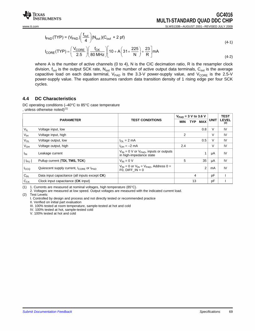
outPAD PAD out out
fI (TYP) = (V ) (N )(C + 2 pf)
4
æ öç ÷è ø (4-1)
CORE CKCORE
V f 225 23I (TYP) 10 A 31 mA
2.5 80 MHz N R
é ùæ öæ ö æ ö= + + +ç ÷ ê úç ÷ ç ÷
è øè øè ø ë û (4-2)
4.4 DC Characteristics
GC4016MULTI-STANDARD QUAD DDC CHIP
www.ti.com SLWS133B–AUGUST 2001–REVISED JULY 2009
where A is the number of active channels (0 to 4), N is the CIC decimation ratio, R is the resampler clockdivision, fout is the output SCK rate, Nout is the number of active output data terminals, Cout is the averagecapacitive load on each data terminal, VPAD is the 3.3-V power-supply value, and VCORE is the 2.5-Vpower-supply value. The equation assumes random data transition density of 1 rising edge per four SCKcycles.
DC operating conditions (–40°C to 85°C case temperature, unless otherwise noted) (1)
VPAD = 3 V to 3.6 V TESTPARAMETER TEST CONDITIONS UNIT LEVELMIN TYP MAX (2)
VIL Voltage input, low 0.8 V IVVIH Voltage input, high 2 V IVVOL Voltage output, low IOL = 2 mA 0.5 V IVVOH Voltage output, high IOH = –2 mA 2.4 V IV
VIN = 0 V or VPAD, inputs or outputsIIN Leakage current 1 µA IVin high-impedance state| IPU | Pullup current (TDI, TMS, TCK) VIN = 0 V 5 35 µA IV
VIN = 0 or VIN = VPAD, Address 0 =ICCQ Quiescent supply current, ICORE or IPAD 2 mA IVF0, DIFF_IN = 0CIN Data input capacitance (all inputs except CK) 4 pF ICCK Clock input capacitance (CK input) 13 pF I
(1) 1. Currents are measured at nominal voltages, high temperature (85°C).2. Voltages are measured at low speed. Output voltages are measured with the indicated current load.
(2) Test Levels:I. Controlled by design and process and not directly tested or recommended practiceII. Verified on initial part evaluationIII. 100% tested at room temperature, sample-tested at hot and coldIV. 100% tested at hot, sample-tested coldV. 100% tested at hot and cold
Submit Documentation Feedback Specifications 69

4.5 AC Characteristics
GC4016MULTI-STANDARD QUAD DDC CHIPSLWS133B–AUGUST 2001–REVISED JULY 2009 www.ti.com
AC operating conditions (–40°C to 85°C case temperatureacross recommended voltage range, unless otherwise noted)
MIN MAX TESTPARAMETER UNIT LEVEL (1)
fCK Clock frequency See 100 MHz IV(2) (3)
tCKL/H Clock low or high period 3 ns IVClock duty cycle (tCKH as a percentage of the clock period) 70% II
tRF Clock rise and fall times (VIL to VIH) 2 ns ItSU Input setup before CK goes high (AIN, BIN, CIN, DIN, or SI), single-ended 2 ns IVtHD Input hold time after CK goes high 0.8 ns IVtDLY Data output delay from rising edge of CK (P[0:23], SFS, SCK, RDY, or SO) 1 5 ns IVtSKEW Data output skew from rising edge of SCK (P[0:23], SFS, or RDY) –2.5 2.5 ns IVfJCK JTAG clock frequency 40 MHz IVtJCKL JTAG clock low period (below VIL) 10 ns IVtJCKH JTAG clock high period (above VIH) 10 ns IVtJSU JTAG input (TDI or TMS) setup before TCK goes high 1 ns IVtHD JTAG input (TDI or TMS) hold time after TCK goes high 10 ns IVtDLY JTAG output (TDO) delay from rising edge of TCK 10 ns IVtCSU Control setup during reads or writes. See Figure 1-2 and Figure 1-3. 2 ns IVtEWCSU Control data setup during writes (edge mode). See Figure 1-3. 4 ns IVtCHD Control hold during writes. See Figure 1-2 and Figure 1-3. 1 ns IV
Control strobe (CS and WR low) pulse duration (write operation). See Figure 1-2tCSPW 20 ns IVand Figure 1-3.Control output delay CS and RD low and A stable to C (read operation). SeetCDLY 12 ns IVFigure 1-2 and Figure 1-3.
tREC Control recovery time between reads or writes. See Figure 1-2 and Figure 1-3. 20 ns ICore dynamic supply current nominal voltages, 100 MHz, four channels active,ICDYN 100 390 mA IVresampler at full speed, high temperature.
(1) Test Levels:I. Controlled by design and process and not directly tested or recommended practiceII. Verified on initial part evaluationIII. 100% tested at room temperature, sample-tested at hot and coldIV. 100% tested at hot, sample-tested coldV. 100% tested at hot and cold
(2) The minimum clock rate must satisfy fCK/(4N) > 10 kHz, where N is the CIC decimation ratio.(3) Timing between signals is measured from mid-voltage (VPAD/2) to mid-voltage. Output loading is a 50-Ω transmission line.
Specifications70 Submit Documentation Feedback
5 Application Notes
5.1 Power and Ground Connections
5.2 Static-Sensitive Device
5.3 Moisture-Sensitive Package
5.4 Thermal Management
5.5 Example CFIR Filter Sets
GC4016MULTI-STANDARD QUAD DDC CHIP
www.ti.com SLWS133B–AUGUST 2001–REVISED JULY 2009
The GC4016 chips are very high-performance chips which require solid power and ground connections toavoid noise on the VCORE, VPAD and GND terminals. If possible, the GC4016 chip should be mountedon a circuit board with dedicated power and ground planes and with at least two decoupling capacitors(0.01 µF) adjacent to each side of the chip, one for VCORE and one for VPAD.
NOTETHE GC4016 CHIP MAY NOT OPERATE PROPERLY IF THESE POWER ANDGROUND GUIDELINES ARE VIOLATED.
The GC4016 chips are fabricated in a high-performance CMOS process. Consequently, they are sensitiveto the high-voltage transients caused by static electricity. These parts can be permanently damaged bystatic electricity and should only be handled in static-free environments. See the Absolute MaximumRatings, Section 4.1.
The GC4016 comes in a level-2 moisture-sensitive package. Dry-pack storage is required prior toassembly. If parts are stored out of dry pack for more than 72 hours, then parts must be baked for 24hours at 100°C prior to assembly.
The parameters in Section 4 are tested at a case temperature of 100°C. In any case, the junctiontemperature must be kept below 125°C for reliable operation. The junction temperature can be calculatedbased on the three heat transfer modes, a combination of θJB (conduction—junction to ground ball tocircuit board), θJC (conduction—junction to case to heatsink), and θJA (convection—junction to ambient). Aheat sink and/or air flow can be used to lower the junction temperature.
For example, the GC4016 chip operating in the GSM mode, as described in Section 5.10, consumes0.3 W of power. The junction-to-ambient rise of the PBGA160 package is 32°Cper W. This represents a rise of 10°C over ambient. This means that under these conditions, the ambienttemperature must be less than 90°C to keep the junction temperature below 100°C. Air flow decreases thethermal resistance by 10% to 40%, allowing ambient temperatures up to 96°C. Increasing the decimationratio (N) or decreasing the number of active channels (A) also allows a higher ambient temperature.
The CFIR filter must be flat over the output pass band of interest, and have a stop band that rejectsout-of-band signals which fall into the pass band of interest. The spectral requirements of this filter areshown in Figure 1-10. The CFIR filter must also compensate for the pass-band rolloff of the CIC filter. Thefollowing filters compensate for the CIC rolloff and provide pass-band bandwidths which are between 17%and 150% of the downconverter output sample rate (the PFIR output rate before resampling).
The filter taps can be copied from Table 5-1 or downloaded from GC4016 Filter Taps in the TechnicalDocuments section of the GC4016 Designer's Utility KitWeb page. The filter taps are available in two file formats. The first, <filter_name>.taps, is an ASCII listingof the taps. The second, <filter_name>.cmd, is a command file which could be used to write the filter tapsinto a GC4016 chip. The commands are formatted as write <address> <data_byte>, where <address> and<data_byte> are unsigned hex integers.
Submit Documentation Feedback Application Notes 71

5.6 Example PFIR Filter Sets
GC4016MULTI-STANDARD QUAD DDC CHIPSLWS133B–AUGUST 2001–REVISED JULY 2009 www.ti.com
The recommended default filter is cfir_80, which is flat out to 80% of the usable bandwidth of the channeloutput. The narrower filters have less ripple and better out-of-band rejection. The wider filters (100% and150%) are designed for the single-wideband-output-per-chip mode, where all four channels are used asone wideband channel. These modes have more ripple and less out-of-band rejection than thenarrowband filters.
Table 5-1. Example CFIR FiltersUsable Pass- Pass-Band Stop-Stop-Band CFIR GainName Output Band Ripple (pk to Band Applications Taps (First 11)Start (CFIR_SUM)Bandwidth Cutoff pk) Rejection
cfir_17 17% 0.085 0.01 dB 1.5 110 dB 2.0413 8× oversampled 5 39 –166 –1301 –3009(133,781) outputs –2848 1280 9009 18,952
28,546 32,767
cfir_34 34% 0.17 0.0 1dB 1.5 110 dB 1.5429 4× oversampled –24 74 494 548 –977 –3416(101,113) outputs, 2X GSM or –3672 1525 13,074 26,547
EDGE outputs 32,767
cfir_68 68% 0.34 0.02 dB 1.55 100 dB 1.2665 2× oversampled 12 –93 –62 804 1283 –1273(83,001) outputs, 1X GSM or –5197 –3512 8332 24,823
EDGE outputs 32,767
cfir_80 80% 0.4 0.025 dB 1.5 100 dB 0.9899 1.5× oversampled 5 –8 –172 –192 806 1493(default) (64,877) outputs; default filter –1889 –6182 1085 21,109
for most applications 32,767
cfir_100 100% 0.5 0.08 dB 1.5 100 dB 0.9109 Single wideband DDC –3 40 –75 –437 291 1951(59,695) mode (See –489 –6365 –1185 19,736
Section 1.2.4.2) 32,767
cfir_150 150% 0.75 0.6 dB 1.25 60 dB 0.9154 Single wideband DDC 47 –102 –1184 –1274 1487(59,993) mode (See 3243 –1798 –7760 15 20,939
Section 1.2.4.2) 32,767
Key:The usable output bandwidth is the pass-band bandwidth expressed as a percentage of the DDC-channel output sample rate.The pass-band cutoff frequency is relative to the DDC-channel output sample rate.The stop-band start frequency is relative to the DDC-channel output sample rate.The taps are the first 11 taps of the 21-tap filter. The final 10 taps are a mirror image of the first 10 taps. The center taps are scaled to the full-scale positivevalue of 32,767.The gain is CFIR_SUM/65,536; the value in parentheses is the CFIR_SUM.
The spectral requirements of the PFIR filter are shown in Figure 1-11. The filters in Table 5-2 providepass-band bandwidths which are between 17% and 150% of the downconverter-channel output samplerate (before resampling).
The filter taps can be copied from Table 5-2 or downloaded from the GC4016 Filter Taps in the TechnicalDocuments section of the GC4016 Designer's Utility KitWeb page. The filter taps are available in two file formats. The first, <filter_name>.taps, is an ASCII listingof the taps. The second, <filter_name>.cmd, is a command file which could be used to write the filter tapsinto a GC4016 chip. The commands are formatted as write <address> <data_byte>, where <address> and<data_byte> are unsigned hex integers.
Application Notes72 Submit Documentation Feedback
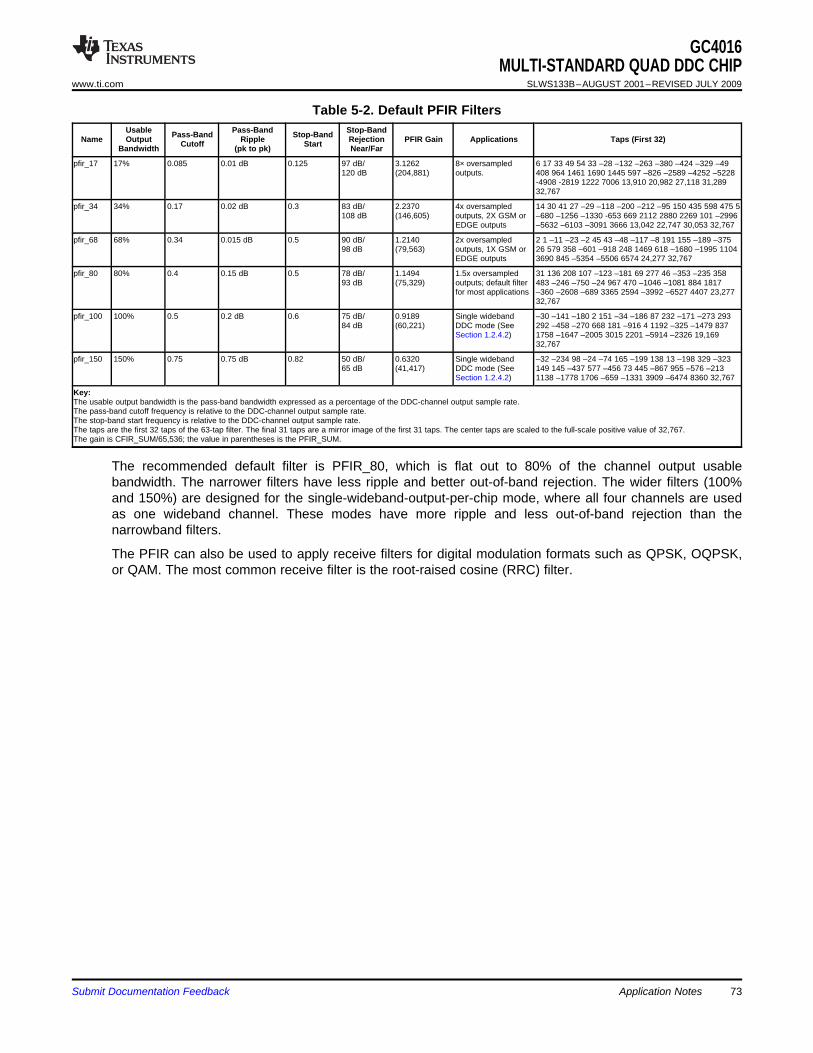
GC4016MULTI-STANDARD QUAD DDC CHIP
www.ti.com SLWS133B–AUGUST 2001–REVISED JULY 2009
Table 5-2. Default PFIR FiltersUsable Pass-Band Stop-BandPass-Band Stop-BandName Output Ripple Rejection PFIR Gain Applications Taps (First 32)Cutoff StartBandwidth (pk to pk) Near/Far
pfir_17 17% 0.085 0.01 dB 0.125 97 dB/ 3.1262 8× oversampled 6 17 33 49 54 33 –28 –132 –263 –380 –424 –329 –49120 dB (204,881) outputs. 408 964 1461 1690 1445 597 –826 –2589 –4252 –5228
-4908 -2819 1222 7006 13,910 20,982 27,118 31,28932,767
pfir_34 34% 0.17 0.02 dB 0.3 83 dB/ 2.2370 4x oversampled 14 30 41 27 –29 –118 –200 –212 –95 150 435 598 475 5108 dB (146,605) outputs, 2X GSM or –680 –1256 –1330 -653 669 2112 2880 2269 101 –2996
EDGE outputs –5632 –6103 –3091 3666 13,042 22,747 30,053 32,767
pfir_68 68% 0.34 0.015 dB 0.5 90 dB/ 1.2140 2x oversampled 2 1 –11 –23 –2 45 43 –48 –117 –8 191 155 –189 –37598 dB (79,563) outputs, 1X GSM or 26 579 358 –601 –918 248 1469 618 –1680 –1995 1104
EDGE outputs 3690 845 –5354 –5506 6574 24,277 32,767
pfir_80 80% 0.4 0.15 dB 0.5 78 dB/ 1.1494 1.5x oversampled 31 136 208 107 –123 –181 69 277 46 –353 –235 35893 dB (75,329) outputs; default filter 483 –246 –750 –24 967 470 –1046 –1081 884 1817
for most applications –360 –2608 –689 3365 2594 –3992 –6527 4407 23,27732,767
pfir_100 100% 0.5 0.2 dB 0.6 75 dB/ 0.9189 Single wideband –30 –141 –180 2 151 –34 –186 87 232 –171 –273 29384 dB (60,221) DDC mode (See 292 –458 –270 668 181 –916 4 1192 –325 –1479 837
Section 1.2.4.2) 1758 –1647 –2005 3015 2201 –5914 –2326 19,16932,767
pfir_150 150% 0.75 0.75 dB 0.82 50 dB/ 0.6320 Single wideband –32 –234 98 –24 –74 165 –199 138 13 –198 329 –32365 dB (41,417) DDC mode (See 149 145 –437 577 –456 73 445 –867 955 –576 –213
Section 1.2.4.2) 1138 –1778 1706 –659 –1331 3909 –6474 8360 32,767
Key:The usable output bandwidth is the pass-band bandwidth expressed as a percentage of the DDC-channel output sample rate.The pass-band cutoff frequency is relative to the DDC-channel output sample rate.The stop-band start frequency is relative to the DDC-channel output sample rate.The taps are the first 32 taps of the 63-tap filter. The final 31 taps are a mirror image of the first 31 taps. The center taps are scaled to the full-scale positive value of 32,767.The gain is CFIR_SUM/65,536; the value in parentheses is the PFIR_SUM.
The recommended default filter is PFIR_80, which is flat out to 80% of the channel output usablebandwidth. The narrower filters have less ripple and better out-of-band rejection. The wider filters (100%and 150%) are designed for the single-wideband-output-per-chip mode, where all four channels are usedas one wideband channel. These modes have more ripple and less out-of-band rejection than thenarrowband filters.
The PFIR can also be used to apply receive filters for digital modulation formats such as QPSK, OQPSK,or QAM. The most common receive filter is the root-raised cosine (RRC) filter.
Submit Documentation Feedback Application Notes 73

5.7 Overall Spectral Responses of Example Filters
−120
−110
−100
−90
−80
−70
−60
−50
−40
−30
−20
−10
0
0 1 2 3 4
Normalized Frequency
P −
Pow
er −
dB
G005
17% ModeOutput Sample Rate = 1
−120
−110
−100
−90
−80
−70
−60
−50
−40
−30
−20
−10
0
0 1 2 3 4
Normalized Frequency
P −
Pow
er −
dB
G006
34% ModeOutput Sample Rate = 1
−120
−110
−100
−90
−80
−70
−60
−50
−40
−30
−20
−10
0
0 1 2 3 4
Normalized Frequency
P −
Pow
er −
dB
G007
68% ModeOutput Sample Rate = 1
−120
−110
−100
−90
−80
−70
−60
−50
−40
−30
−20
−10
0
0 1 2 3 4
Normalized Frequency
P −
Pow
er −
dB
G008
80% ModeOutput Sample Rate = 1
GC4016MULTI-STANDARD QUAD DDC CHIPSLWS133B–AUGUST 2001–REVISED JULY 2009 www.ti.com
Overall Out-of-Band Rejection—17% Mode Overall Out-of-Band Rejection—34% Mode
Figure 5-1. cfir_17 With pfir_17 Figure 5-2. cfir_34 With pfir_34
Overall Out-of-Band Rejection—68% Mode Overall Out-of-Band Rejection—80% Mode
Figure 5-3. cfir_68 With pfir_68 Figure 5-4. cfir_80 With pfir_80
Application Notes74 Submit Documentation Feedback

−120
−110
−100
−90
−80
−70
−60
−50
−40
−30
−20
−10
0
0 1 2 3 4
Normalized Frequency
P −
Pow
er −
dB
G009
100% ModeOutput Sample Rate = 1
−120
−110
−100
−90
−80
−70
−60
−50
−40
−30
−20
−10
0
0 1 2 3 4
Normalized FrequencyP
− P
ower
− d
BG010
150% ModeOutput Sample Rate = 1
5.8 Example Resampler Configurations
5.8.1 Bypass Mode
5.8.2 Resampling Modes
GC4016MULTI-STANDARD QUAD DDC CHIP
www.ti.com SLWS133B–AUGUST 2001–REVISED JULY 2009
Overall Out-of-Band Rejection—100% Mode Overall Out-of-Band Rejection—150% Mode
Figure 5-5. cfir_100 With pfir_100 Figure 5-6. cfir_150 With pfir_150
This section describes some commonly used resampler configurations and the filter coefficient sets usedfor them.
The resampler is bypassed by using a configuration which has h0 set to 1024, all other taps set to zero,NMULT set to 7, NO_SYM_RES set to 1, FINAL_SHIFT set to 5, and RATIO set to 226 (0x0400 0000).Note that the NDELAY term in the RES_GAIN equation does not apply in this case and should be set tounity in the gain equation. The resampler control register setting for this mode are shown in Table 5-3.
Table 5-3. Resampler Bypass ModeAddress 16 17 18 19 20 21 22 23 24 25 26 27 28 29 30 31
Page 32 00 04 00Pages 0033–63Page 64 23 46 00 35 E4 70 00 00 UnusedPage 65 00 00 00 04 00 00 00 04 00 00 00 04 00 00 00 04
Several resampler configurations are summarized in Table 5-4. These configurations use the defaultvalues for the resampler controls except for NMULT in address 17, which must be set to the value inTable 5-4. The defaults (hex) are 23, NM, 00, 34, E4, 00, 00 and 00, respectfully for addresses 16 through23 of page 64. NM is NMULT – 1.
Table 5-4. Resampler ModesConfiguration PB Ripple Image RejectionNMULT %BW RES_SUM ApplicationName (dB) (dB)Configurations with NDELAY = 64These offer the best resampling phase jitter performance (–48 dB in-band noise), but the % input bandwidth must be 60% or less.
Submit Documentation Feedback Application Notes 75

5.9 GC4016 Configuration Generator
GC4016MULTI-STANDARD QUAD DDC CHIPSLWS133B–AUGUST 2001–REVISED JULY 2009 www.ti.com
Table 5-4. Resampler Modes (continued)Configuration PB Ripple Image RejectionNMULT %BW RES_SUM ApplicationName (dB) (dB)res_6x64_60 6 0.18 52 134,786 Use if NMULT must be 6
60res_7x64_60 7 0.16 55 138,292 Use if NMULT must be less than 8
SUGGESTED DEFAULT: best 60% bandwidthres_8x64_60 60 0.03 62 134,782 mode; adequate for most applications8res_8x64_80 80 0.7 43 139,894 An 80% mode with NMULT = 8
Configurations with NDELAY = 32These offer higher % bandwidth, but fewer resampling delays (-42 dB in-band jitter noise)
Best 60% mode for interpolating by integerres_9x32_60 9 60 0.01 63 64,700 amountsres_12x32_80 12 80 0.11 48 65,610 Alternate if NMULT must be less than 15
Best 80% mode; very good for interpolating byres_15x32_80 15 0.05 58 66,482 integer amountsConfigurations with NDELAY = 16These are restricted to single- or dual-channel modes; very good for interpolating by integer amounts.
Good filter, but only for single- or dual-channelres_19x16_80 19 80 0.02 65 32,988 modes
The %BW column reflects the percentage pass band of the signal relative to the sample rate going intothe resampler. The resampler response is flat over this bandwidth to within the pass-band ripple indicatedin Table 5-4. The image rejection is the amount that the resampling images are rejected relative to thesignal.
The filter taps for these configurations can be downloaded from GC4016 Filter Taps in the TechnicalDocuments section of the GC4016 Designer's Utility KitWeb page. The filter taps are available in two file formats. The first, <filter_name>.taps, is an ASCII listingof the taps. The second, <filter_name>.cmd, is a command file which could be used to write the filter tapsinto a GC4016 chip. The commands are formatted as write <address> <data_byte>, where <address> and<data_byte> are unsigned hex integers.
A GC4016 configuration generator is available from GC4016 Programming Software in the TechnicalDocuments section of the GC4016 Designer's Utility KitWeb page. The program is described as follows.Usage: cmd4016 [-gc100 | -TI | -sim] <config_file>
where <config_file> is a file containing a list of control register settings of the form:<parameter> <value>print [gc100 | TI | sim]channel [0-3]copy_channel [0-3]cfir_coef <file>pfir_coef <file>res_coef <file>
where <parameter> is one of the GC4016 control register fields identified in the data manual or quickreference guide.
cmd4016 reads the file of control register settings and creates output files which summarize the controlregister values needed to program the chip. The program creates config_file.tbl, which contains asummary of all of the control register settings in a table format.
A second file is created which is in a format suitable for programming the chip. Three formats aresupported: gc100, TI, and sim. The format either is chosen on the command line, or is chosen using theprint [gc100 | TI | sim] command. These options create config_file.gc100, config_file.ti, andconfig_file.sim output files, respectively.
The gc100 format is used by the gc100 test-card interface. This format contains commands of the form:
Application Notes76 Submit Documentation Feedback

5.10 Example GSM Application
5.10.1 GSM Filter Response
GC4016MULTI-STANDARD QUAD DDC CHIP
www.ti.com SLWS133B–AUGUST 2001–REVISED JULY 2009
write <address> <data>
orwrite_block <starting_address> <data0> <data1> <data2> ...
The TI format is for use with the 4-bit addressing mode and contains commands of the form:<address> <data>
The sim format is used by the ifan simulator and contains commands of the form:writec <address> <data>
The 4_bit_address mode is required in the TI mode; it is illegal in the gc100 and sim modes. A warning isprinted and the appropriate 4_bit_address mode is forced if this is violated. cmd4016 then checks theconfiguration for proper configurationand calculates the gains throughout the chip.
Example configuration files can also be downloaded from the GC4016 Diagnostic Configurations andChecksums section of the GC4016 Designer's Utility Kit Web page.
This section describes how to configure the chip to downconvert GSM (or EDGE) signals and meet thestringent GSM processing specifications. The desired GSM Specifications are shown in Table 5-5.
Table 5-5. Desired GSM SpecifictionsSpecification Value Comment
Clock (CK) 69.333 MHz = 256 × 270.833 kHz Can be any value equal to 4 × N × B, where N is the CIC decimationratio and B is the GSM bit rate of 270.833 kHz.
Input sample rate Same as clock rate Can be 1/2, 1/3, 1/4, ..., 1/N times the clock rate using the zero-padfeature.
Input format A port, 14-bit, 2s-complement Can be modified as desiredSpurious-free ≥110 dB The GC4016 NCO provides more than 115 dB of spurious- freedynamic range dynamic range.Output sample rate 270.833 kHz, complex data Can be 2×, 4×, 8×, or any multiple of this rate by changing the
resampler ratiosPass-band width 160 kHz The filter response must be flat over this bandwidth to within the
pass-band ripple.Pass-band ripple < 0.1 dB peak-to-peak To meet the GSM BER specificationStop-band rejection Set by GSM specification See the GSM adjacent channel and blocker mask in Figure 5-7.Output format Four serial streams, 24 bit I and Q Can be modified as desired
data
Figure 5-7 shows the overall response using the cfir_68 CFIR filter and a set of PFIR coefficients tuned forGSM. The GSM out-of-band rejection mask is also shown. The pass-band ripple is less than 0.1 dB (peakto peak). The pass-band ripple specification for GSM is not directly specified. Instead, it is specified interms of bit error rate (BER). Trade-offs between transition bandwidth and pass-band ripple in order tooptimize the BER can easily be made by reprogramming the PFIR filter.
Submit Documentation Feedback Application Notes 77

−120
−110
−100
−90
−80
−70
−60
−50
−40
−30
−20
−10
0
0 200 400 600 800 1000
f − Frequency − kHz
P −
Pow
er −
dB
G011
Blocker Requirements
GSM ModeOutput Sample Rate = 270.833 kHz
Adjacent Band Rejection
−1.0
−0.9
−0.8
−0.7
−0.6
−0.5
−0.4
−0.3
−0.2
−0.1
0.0
0.1
0 10 20 30 40 50 60 70 80 90 100
f − Frequency − kHzP
− P
ower
− d
BG012
GSM ModeOutput Sample Rate = 270.833 kHz
5.10.2 Oversampling Using the Resampler
5.10.3 Gain
GC4016MULTI-STANDARD QUAD DDC CHIPSLWS133B–AUGUST 2001–REVISED JULY 2009 www.ti.com
GC4017 Out-of-Band Response—GSM Mode GC4017 Pass-Band Response—GSM Mode
Figure 5-7. Frequency Response for the Example GSM Application
The PFIR coefficients are:132 182 1 –309 –330 119 560 343 –424 –834 –278 696 960 149 –916 –1132 –212 1075 1514 421–1518 –2374 –673 2529 3817 726 –4796 –6888 –650 12,967 26,898 32,767
These coefficients are available frm GC4016 Filter Taps in the Technical Documents section of theGC4016 Designer's Utility KitWeb page as pfir_gsm.taps. The PFIR_SUM for this set of coefficients is 96,277.
This example assumes the input sample rate is equal to 4 × N × B, where N is the decimation in the CICfilter (See Section 3.6) and B is the GSM bit rate (270.833 kHz). The outputs are one complex sample perbit (270.833 kHz) with the resampler set interpolate by unity (no interpolation). The output rate can bedoubled or quadrupled as desired by changing the resampler ratio. The resampler uses the configurationres_8x64_60. (See Section 5.8). This configuration introduces 0.03 dB of pass-band ripple and –62 dB ofin-band noise, neither being large enough to affect the BER.
The resampler ratio for one sample per bit (270.833 kHz) is 0x0400 0000. It is 0x0200 0000 for twosamples per bit (541.666 kHz), and it is 0x01000 0000 for four samples per bit (1.08333 MHz).
The example configuration assumes a CIC decimation of N = 64, which corresponds to an ADC clock rate(CK) of 69.333248 MHz. The values of SCALE and BIG_SCALE must be chosen to satisfy: (SHIFT +SCALE + 6 × BIG_SCALE) ≤ (62 – 5log2N). N is 64 and SHIFT is 4, so (SCALE + 6 × BIG_SCALE) ≤ 28,which is satisfied by setting SCALE = 4 and BIG_SCALE = 4. If other values of N are chosen, thenSCALE and BIG_SCALE must be modified as necessary. The overall gain is adjusted using FINE_GAINand FINAL_SHIFT. The overall gain is:
Application Notes78 Submit Documentation Feedback

( )
( )
5 (SHIFT SCALE 6 BIG_SCALE 62) COARSE
FINAL_SHIFT
1 CFIR_SUMGAIN N 2 2
NZEROS 1 65,536
CFIR_SUM PFIR_SUM FINE_GAIN RES_SUM2
65,536 65,536 1024 32,768 NDELAY
+ + ´ -ì ü æ öæ ö= ´í ý ç ÷ç ÷+è ø è øî þ
æ öæ ö æ öæ öç ÷ç ÷ ç ÷ç ÷ ´è øè øè ø è ø
5.10.4 GSM Configuration
5.11 Example IS-136 DAMPS Application
GC4016MULTI-STANDARD QUAD DDC CHIP
www.ti.com SLWS133B–AUGUST 2001–REVISED JULY 2009
where NZEROS = 0, N = 64, SHIFT = 4, SCALE = 4, BIG_SCALE = 4, COARSE = 0,CFIR_SUM = 83,001, PFIR_SUM = 96,277, RES_SUM = 134,782, and NDELAY = 64. Because of theloss of 1/2 when converting real data to complex, the desired gain is 2. This can be achieved by settingFINE_GAIN to 1070 and FINAL_SHIFT to 4.
The control register settings for this example are shown in Table 5-6. It is assumed that output terminalSO is tied to input terminal SIA.
Table 5-6. Example GSM ConfigurationGLOBAL REGISTERS
Address 0 1 2 3 4 5 6 7
F8 00 00 – 27 DC 00 00 After configuration, set address 0 to 08, then set address 5 to5C.
PAGED REGISTERS
Address 16 17 18 19 20 21 22 23 24 25 26 27 28 29 30 31
CH A Pages 0, 1 Load CFIR coefficients: cfir_68.taps
Pages 2–5 Load PFIR coefficients: pfir_gsm.taps
Page 6 00 00 FREQ Unused
Page 7 0C 77 00 20 22 3F 70 64 00 00 00 00 1D – 2E 04
CH B Pages 8, 9 Load CFIR coefficients: cfir_68.taps
Pages 10–13 Load PFIR coefficients: pfir_gsm.taps
Page 14 00 00 FREQ Unused
Page 15 0C 77 00 20 22 3F 70 64 00 00 00 00 1D – 2E 04
CH C Pages 16, 17 Load CFIR coefficients: cfir_68.taps
Pages 18–21 Load PFIR coefficients: pfir_gsm.taps
Page 22 00 00 FREQ Unused
Page 23 0C 77 00 20 22 3F 70 64 00 00 00 00 1D – 2E 04
CH D Pages 24, 25 Load CFIR coefficients: cfir_68.taps
Pages 26–29 Load PFIR coefficients: pfir_gsm.taps
Page 30 00 00 FREQ Unused
Page 31 0C 77 00 20 22 3F 70 64 00 00 00 00 1D – 2E 04
RES Pages 32–63 Load resampler coefficients: res_8x64_60.taps
Page 64 23 07 00 34 E4 00 00 00 Unused
Page 65 00 00 00 04 00 00 00 04 00 00 00 04 00 00 00 04
OUT Page 98 7F 40 28 01 E9 B0 E4 10 32 54 76 02 Unused
This section describes how to configure the chip to downconvert DAMPS signals, apply theroot-raised-cosine receive filter, and output samples at two times, four times, or eight times the DAMPSsymbol rate. The desired DAMPS specifications are:
Table 5-7. Desired DAMPS SpecificationsSpecification Value Comment
Clock (CK) 62.208 MHz = 8 × 320 × 24.3 kHz Can be any value equal to 8 × N × B, where N is the CIC decimationratio and B is the DAMPS symbol rate of 24.3 kHz
Submit Documentation Feedback Application Notes 79

5.11.1 DAMPS Filter Response
−120
−110
−100
−90
−80
−70
−60
−50
−40
−30
−20
−10
0
0 30 60 90 120 150 180 210 240 270 300
f – Frequency – kHz
P –
Pow
er –
dB
G013
Rejection Mask
DAMPS 2 ModeOutput Sample Rate = 48.6 kHz
GC4016MULTI-STANDARD QUAD DDC CHIPSLWS133B–AUGUST 2001–REVISED JULY 2009 www.ti.com
Table 5-7. Desired DAMPS Specifications (continued)Specification Value Comment
Input sample rate Same as clock rate Can be 1/2, 1/3, 1/4, ... 1/N of the clock rate by using the zero-padfeature.
Input format A port, 14-bit, 2s-complement Can be modified as desiredSpurious-free ≥110 dB The GC4016 NCO provides more than 115 dB of spurious-freedynamic range dynamic range.Output sample rate 48.6 kHz, complex data (2×) Can be 4×, 8× or any multiple of the symbol rate by changing the
resampler ratiosPass-band response RRC with alpha = 0.35 Matches the required receive filterStop-band rejection Set by DAMPS specification See the DAMPS rejection mask in Figure 5-8.Output format Four serial streams, 24-bit I and Q data Can be modified as desired
Figure 5-8 shows the overall response using the cfir_68 CFIR filter and a set of RRC PFIR coefficientstuned for 2× oversampled output data. The DAMPS out-of-band rejection mask is also shown.
Overall Out-of-Band Rejection—DAMPS 2× Mode
Figure 5-8. Frequency Response for the Example DAMPS Application
The RRC PFIR coefficients are:–12 –117 –113 8 127 112 –38 –175 –134 82 275 224 –71 –348 –307 61 398 286 –286 –761 –442 7661954 1708 –660 –4042 –5641 –2533 6187 18,177 28,625 32,767
These coefficients are available from GC4016 Filter Taps in the Technical Documents section of theGC4016 Designer's Utility KitWeb page as pfir_damps_2x.taps. The PFIR_SUM for this set of coefficients is 119,387.
Application Notes80 Submit Documentation Feedback

5.11.2 Oversampling Using the Resampler
5.11.3 Gain
( )
( )
5 (SHIFT SCALE 6 BIG_SCALE 62) COARSE
FINAL_SHIFT
1 CFIR_SUMGAIN N 2 2
NZEROS 1 65,536
CFIR_SUM PFIR_SUM FINE_GAIN RES_SUM2
65,536 65,536 1024 32,768 NDELAY
+ + ´ -ì ü æ öæ ö= ´í ý ç ÷ç ÷+è ø è øî þ
æ öæ ö æ öæ öç ÷ç ÷ ç ÷ç ÷ ´è øè øè ø è ø (5-1)
5.11.4 DAMPS Configuration
GC4016MULTI-STANDARD QUAD DDC CHIP
www.ti.com SLWS133B–AUGUST 2001–REVISED JULY 2009
This example assumes the input sample rate is equal to 8 × N × B, where N is the decimation in the CICfilter (See Section 3.6) and B is the DAMPS symbol rate (24.3 kHz). The outputs are two complexsamples per symbol (48.6 kHz) with the resampler set to interpolate by unity (no interpolation). The outputrate can be doubled or quadrupled as desired by changing the resampler ratio. The resampler uses theconfiguration res_15x32_80. (See Section 5.8). This configuration introduces 0.05 dB of pass-band rippleand –58 dB of in-band noise, neither being large enough to affect the BER.
The resampler ratio for two samples per symbol (48.6 kHz) is 0x0400 0000, for four samples per symbol(97.2 kHz) is 0x0200 0000, and for eight samples per symbol (194.4 kHz) is 0x0100 0000.
The example configuration assumes a CIC decimation of N = 320, which corresponds to an ADC clockrate (CK) of 62.208 MHz. The values of SCALE and BIG_SCALE must be chosen to satisfy: (SHIFT +SCALE + 6 × BIG_SCALE) ≤ (62 – 5log2N). N is 320 and SHIFT = 4, so (SCALE + 6 × BIG_SCALE) ≤16.4, which is satisfied by setting SCALE = 4 and BIG_SCALE = 2. If other values of N are chosen, thenSCALE and BIG_SCALE must be modified as necessary. The overall gain is adjusted using FINE_GAINand FINAL_SHIFT. The overall gain is:
where NZEROS = 0, N = 320, SHIFT = 4, SCALE = 4, BIG_SCALE = 2, COARSE = 0,CFIR_SUM = 83,001, PFIR_SUM = 119,387, RES_SUM = 66,554, and NDELAY = 32. Because of theloss of 1/2 when converting real data to complex, the desired gain is 2. This can be achieved by settingFINE_GAIN to 1147 and FINAL_SHIFT to 4.
The control register settings for this example are shown in Table 5-8. It is assumed that output terminalSO is tied to input terminal SIA.
Table 5-8. Example DAMPS ConfigurationGLOBAL REGISTERS
Address 0 1 2 3 4 5 6 7
F8 00 00 – 27 DC 00 00 After configuration, set address 0 to 08, then set address 5 to5C.
PAGED REGISTERS
Address 16 17 18 19 20 21 22 23 24 25 26 27 28 29 30 31
CH A Pages 0, 1 Load CFIR coefficients: cfir_68.taps
Pages 2–5 Load PFIR coefficients: pfir_damps_2x.taps
Page 6 00 00 FREQ Unused
Page 7 0C 77 00 20 22 3F 71 54 00 00 00 00 1D – 7B 04
CH B Pages 8, 9 Load CFIR coefficients: cfir_68.taps
Pages 10–13 Load PFIR coefficients: pfir_damps_2x.taps
Page 14 00 00 FREQ Unused
Page 15 0C 77 00 20 22 3F 71 54 00 00 00 00 1D – 7B 04
CH C Pages 16, 17 Load CFIR coefficients: cfir_68.taps
Pages 18–21 Load PFIR coefficients: pfir_damps_2x.taps
Page 22 00 00 FREQ Unused
Page 23 0C 77 00 20 22 3F 71 54 00 00 00 00 1D – 7B 04
Submit Documentation Feedback Application Notes 81

GC4016MULTI-STANDARD QUAD DDC CHIPSLWS133B–AUGUST 2001–REVISED JULY 2009 www.ti.com
Table 5-8. Example DAMPS Configuration (continued)GLOBAL REGISTERS
CH D Pages 24, 25 Load CFIR coefficients: cfir_68.taps
Pages 26–29 Load PFIR coefficients: pfir_damps_2x.taps
Page 30 00 00 FREQ Unused
Page 31 0C 77 00 20 22 3F 71 54 00 00 00 00 1D – 7B 04
RES Pages 32–63 Load resampler coefficients: res_15_32_80.taps
Page 64 23 0E 00 34 E4 00 00 00 Unused
Page 65 00 00 00 04 00 00 00 04 00 00 00 04 00 00 00 04
OUT Page 98 7F 40 28 01 D9 B1 E4 10 32 54 76 02 Unused
Application Notes82 Submit Documentation Feedback

5.12 Example IS-95 NB-CDMA Application
5.12.1 IS-95 Filter Response
−120
−110
−100
−90
−80
−70
−60
−50
−40
−30
−20
−10
0
0 1 2 3 4
f − Frequency − MHz
P −
Pow
er −
dB
G014
IS95 Mode
900 kHz
–87 dB
750 kHz
−3.0
−2.5
−2.0
−1.5
−1.0
−0.5
0.0
0.5
1.0
0.0 0.1 0.2 0.3 0.4 0.5 0.6 0.7
f − Frequency − MHz
P −
Pow
er −
dB
G015
IS95 Mode
615 kHz
GC4016MULTI-STANDARD QUAD DDC CHIP
www.ti.com SLWS133B–AUGUST 2001–REVISED JULY 2009
This section describes how to configure the chip to downconvert IS-95 NB-CDMA signals and outputsamples at two times 2×), four times (4×) or eight times (8×) the IS-95 symbol rate of 1.2288 MHz. Thedesired IS-95 specifications are:
Table 5-9. Desired IS-95 NB-CDMA SpecificationsSpecification Value Comment
Clock (CK) 58.9824 MHz = 48 × 1.2288 MHz Can be any value greater than this, not required to be a multiple of1.2288 MHz.
Input sample rate Same as clock rate Can be 1/2, 1/3, 1/4, ... 1/N times the clock rate using the zero-padfeature
Input format A port, 14-bit, 2s-complement Can be modified as desiredSpurious-free > –110 dB The GC4016 NCO provides more than 115 dB of spurious-freedynamic range dynamic range.Output sample rate 4.9152 MHz, complex data (4×) Can be 2× or 4× multiple of the symbol rate by changing the
resampler ratio. Can be 8× by using the dual-channel mode.Pass-band width 615 kHz 1.25-MHz signal spacingPass-band ripple 0.4 dBStop-band rejection 50 dB at 750 kHz, 87 dB at 900-kHz Far-band rejection > 120 dB
offsetOutput format Parallel output, 24-bit I and Q data Can be modified as desired, allows simple AGC in an FPGA or ASIC
to 4 or 6 bits.
Figure 5-9 shows the overall response when the channel decimates to 1.5 times the baud rate. This usesthe cfir_68 CFIR filter and the pfir_is95_1.5x PFIR filter. The pass-band ripple is less than 0.4 dB (peak topeak).
Overall Out-of-Band Rejection—IS-95 Mode Overall Pass-Band Response—IS-95 Mode
Figure 5-9. Frequency Response for the Example IS-95 Application
The PFIR coefficients are:
Submit Documentation Feedback Application Notes 83

5.12.2 Oversampling Using the Resampler
5.12.3 Gain
( )
( )
5 (SHIFT SCALE 6 BIG_SCALE 62) COARSE
FINAL_SHIFT
1 CFIR_SUMGAIN N 2 2
NZEROS 1 65,536
CFIR_SUM PFIR_SUM FINE_GAIN RES_SUM2
65,536 65,536 1024 32,768 NDELAY
+ + ´ -ì ü æ öæ ö= ´í ý ç ÷ç ÷+è ø è øî þ
æ öæ ö æ öæ öç ÷ç ÷ ç ÷ç ÷ ´è øè øè ø è ø (5-2)
5.12.4 IS-95 NB-CDMA Configuration
GC4016MULTI-STANDARD QUAD DDC CHIPSLWS133B–AUGUST 2001–REVISED JULY 2009 www.ti.com
–4 –45 –166 –349 –452 –299 96 420 302 –225 –612 –321 471 881 267 –866 –1191 –64 1461 1516–388 –2351 –1826 1303 3804 2088 –3358 –6915 –2266 11,185 26,207 32,767
These coefficients are available from GC4016 Filter Taps in the Technical Documents section of theGC4016 Designer's Utility Kit
Web page as pfir_is95_1.5x.taps. The PFIR_SUM for this set of coefficients is 89,373.
This example assumes the input sample rate is equal to 6 × N × B, where N is the decimation in the CICfilter (See Section 3.6) and B is the IS-95 symbol rate (1.2288 MHz). The PFIR filter output rate is 1.5samples per symbol (1.5×). The outputs are two complex samples per symbol (2.4576 MHz) if theresampler is set to interpolate by 4/3. The output rate can be 4× or 8× as desired by changing theresampler ratio. The resampler uses the configuration res_6x64_60. (See Section 5.8). This configurationintroduces –58 dB of in-band noise, not enough to affect the BER. The spectral effect of the resampler isincluded in Figure 5-9.
The resampler ratio for two samples per symbol (2.4576 MHz) is 0x0300 0000, for four samples persymbol (4.9152 MHz) it is 0x0180 0000, and for eight samples per symbol (9.8304 MHz) it is0x00C0 0000. Note that the resampler can only handle two channels at eight samples per symbol.
Sample rates other than 6 × N × B can be accepted. To use these rates, one must customize the PFIRfilter to match the bandwidth when the sample rate has been decimated by 4 × N, and then the resamplingratio must be adjusted to match the desired output rate.
The example configuration assumes a CIC decimation of N = 8, which corresponds to an ADC clock rate(CK) of 58.9824 MHz. The values of SCALE and BIG_SCALE must be chosen to satisfy: (SHIFT +SCALE + 6 × BIG_SCALE) ≤ (62 – 5log2N). N is 8 and SHIFT = 4, so (SCALE + 6 × BIG_SCALE) ≤ 43,which is satisfied by setting SCALE = 1 and BIG_SCALE = 7. If other values of N are chosen, thenSCALE and BIG_SCALE must be modified as necessary. The overall gain is adjusted using FINE_GAINand FINAL_SHIFT. The overall gain is:
where NZEROS = 0, N = 8, SHIFT = 4, SCALE = 1, BIG_SCALE = 7, COARSE = 0, CFIR_SUM = 83,001,PFIR_SUM = 89,373, RES_SUM = 134,786, and NDELAY = 64. Because of the loss of 1/2 whenconverting real data to complex, the desired gain is 2. This can be achieved by setting FINE_GAIN to1153 and FINAL_SHIFT to 4.
The control register settings for this example are shown in Table 5-10. It is assumed that output terminalSO is tied to input terminal SIA.
Table 5-10. Example IS-95 NB-CDMA ConfigurationGLOBAL REGISTERS
Address 0 1 2 3 4 5 6 7
F8 00 00 – 27 DC 00 00 After configuration, set address 0 to 08, then set address 5 to5C.
PAGED REGISTERS
Address 16 17 18 19 20 21 22 23 24 25 26 27 28 29 30 31
Application Notes84 Submit Documentation Feedback

5.13 UMTS WB-CDMA Applications
5.13.1 UMTS Filter Response
GC4016MULTI-STANDARD QUAD DDC CHIP
www.ti.com SLWS133B–AUGUST 2001–REVISED JULY 2009
Table 5-10. Example IS-95 NB-CDMA Configuration (continued)GLOBAL REGISTERS
CH A Pages 0, 1 Load CFIR coefficients: cfir_68.taps
Pages 2–5 Load PFIR coefficients: pfir_is95_1.5x.taps
Page 6 00 00 FREQ Unused
Page 7 0C 77 22 20 22 07 70 79 00 00 00 00 1D – 81 04
CH B Pages 8, 9 Load CFIR coefficients: cfir_68.taps
Pages 10–13 Load PFIR coefficients: pfir_is95_1.5x.taps
Page 14 00 00 FREQ Unused
Page 15 0C 77 22 20 22 07 70 79 00 00 00 00 1D – 81 04
CH C Pages 16, 17 Load CFIR coefficients: cfir_68.taps
Pages 18–21 Load PFIR coefficients: pfir_is95_1.5x.taps
Page 22 00 00 FREQ Unused
Page 23 0C 77 22 20 22 07 70 79 00 00 00 00 1D – 81 04
CH D Pages 24, 25 Load CFIR coefficients: cfir_68.taps
Pages 26–29 Load PFIR coefficients: pfir_is95_1.5x.taps
Page 30 00 00 FREQ Unused
Page 31 0C 77 22 20 22 07 70 79 00 00 00 00 1D – 81 04
RES Pages 32–63 Load resampler coefficients: res_6x64_60.taps
Page 64 23 05 00 14 E4 70 00 E4 Unused
Page 65 00 00 80 01 00 00 80 01 00 00 80 01 00 00 80 01
OUT Page 98 FF 40 6C 87 EF 00 E4 10 32 54 76 02 Unused
This section describes how to configure the chip to downconvert UMTS WB-CDMA signals and outputsamples at two times or four times the UMTS symbol rate. The desired UMTS specifications are shown inTable 5-11.
Table 5-11. Desired UMTS SpecificationsSpecification Value Comment
Clock (CK) 61.44 MHz = 16 × 3.84 MHz Can be any value greater than this, not required to be a multiple of 3.84MHz.
Input sample rate Same as clock rate May be an integer division of the clock rate (30.72 MHz, 20.48 MHz, etc.)Input format A port, 14-bit, 2s-complement Can be modified as desiredSpurious-free > –80 dB The GC4016 NCO provides more than 115 dB of spurious-free dynamicdynamic range range.Output sample rate 15.36 MSPS, complex data (4×) Can be 2× or 4× multiple of the symbol rate by changing the resampler
ratio. Can do two channels at 2× if the clock rate is greater than92.16 MHz.
Pass-band width 4.6848 MHz RRC filter with alpha = 0.22 gives a bandwidth of 1.22 × 3.84 MHz.Pass-band ripple 0.1 dB Filter gives 0.05-dB pass-band ripple.Stop-band rejection 60 dB at 5 MHz, 80 dB at > 5-MHz Rejection > 80 dB at 2.6-MHz offset
offsetOutput format Parallel output, 16-bit I and Q data Can be modified as desired, allows simple AGC in an FPGA to 4 or 6 bits.
Figure 5-10 shows the overall response using specially tuned CFIR and PFIR filters. The PFIR filter is aspecially optimized root-raised-cosine 63-tap filter with an alpha of 0.22. The filter is designed to have lessthan –50 dB of intersymbol interference (ISI) noise.
Submit Documentation Feedback Application Notes 85

−120
−110
−100
−90
−80
−70
−60
−50
−40
−30
−20
−10
0
0 5 10 15 20 25 30
f − Frequency − MHz
P −
Pow
er −
dB
G016
UMTS Mode (16 Input)Input Sample Rate = 61.44 MHzor 30.72 MHz
2.5 MHz
−1.0
−0.9
−0.8
−0.7
−0.6
−0.5
−0.4
−0.3
−0.2
−0.1
0.0
0.1
0 1 2
f − Frequency − MHzP
− P
ower
− d
BG017
UMTS Mode (16 Input)Output Sample Rate = 15.36 MHz
5.13.2 Oversampling Using the Resampler
5.13.3 Gain
GC4016MULTI-STANDARD QUAD DDC CHIPSLWS133B–AUGUST 2001–REVISED JULY 2009 www.ti.com
GC4016 Out-of-Band Rejection—UMTS Mode (16× Input) GC4016 Pass-Band Response—UMTS Mode (16× Input)
Figure 5-10. Frequency Response for the Example UMTS Application
The PFIR coefficients are:132 182 1 –309 –330 119 560 343 –424 –834 –278 696 960 149 –916 –1132 –212 1075 1514 421–1518 –2374 –673 2529 3817 726 –4796 –6888 –650 12,967 26,898 32,767
These coefficients are available over the Web as pfir_gsm.taps. The PFIR_SUM for this set of coefficientsis 96,277.
This example assumes the input sample rate is equal to 4 × N × B, where N is the decimation in the CICfilter (See Section 3.6) and B is the UMTS symbol rate (3.84 MHz). The outputs are two complex samplesper symbol (7.68 MHz) with the resampler set to interpolate by unity (no interpolation). The output rate canbe doubled or quadrupled as desired by changing the resampler ratio. The resampler uses theconfiguration res_8x64_60. (See Section 5.8). This configuration introduces 0.03 dB of pass-band rippleand –62 dB of in-band noise, neither being large enough to affect UMTS demodulation.
The resampler ratio for two samples per symbol (7.68 MHz) is 0x0400 0000 and for four samples persymbol (15.36 MHz) is 0x0200 0000.
Sample rates other than 4 × N × B can be accepted by adjusting the PFIR filter to match the desired RRCfilter and by using the resampler to adjust the final sample rate to be exactly 2× or 4× the symbol rate.
The example configuration assumes a CIC decimation of N = 4, which corresponds to an ADC clock rate(CK) of 61.44 MHz. The values of SCALE and BIG_SCALE must be chosen to satisfy: (SHIFT + SCALE +6 × BIG_SCALE) ≤ (62 – 5log2N). N is 4 and SHIFT = 4, so (SCALE + 6 × BIG_SCALE ≤ 48, which issatisfied by setting SCALE = 5 and BIG_SCALE = 7, which are their maximum values. If other values of Nare chosen, then SCALE and BIG_SCALE must be modified as necessary. The overall gain is adjustedusing FINE_GAIN and FINAL_SHIFT. The overall gain is:
Application Notes86 Submit Documentation Feedback

( )
( )
5 (SHIFT SCALE 6 BIG_SCALE 62) COARSE
FINAL_SHIFT
1 CFIR_SUMGAIN N 2 2
NZEROS 1 65,536
CFIR_SUM PFIR_SUM FINE_GAIN RES_SUM2
65,536 65,536 1024 32,768 NDELAY
+ + ´ -ì ü æ öæ ö= ´í ý ç ÷ç ÷+è ø è øî þ
æ öæ ö æ öæ öç ÷ç ÷ ç ÷ç ÷ ´è øè øè ø è ø (5-3)
5.13.4 UMTS Configuration
5.14 Diagnostics
GC4016MULTI-STANDARD QUAD DDC CHIP
www.ti.com SLWS133B–AUGUST 2001–REVISED JULY 2009
where NZEROS = 0, N = 4, SHIFT = 4, SCALE = 5, BIG_SCALE = 7, COARSE = 1, CFIR_SUM = 58,827,PFIR_SUM = 61,821, RES_SUM = 134,782, and NDELAY = 64. Because of the loss of 1/2 whenconverting real data to complex, the desired gain is 2. This can be achieved by setting FINE_GAIN to2352 and FINAL_SHIFT to 4.
The control register settings for this example are shown in Table 5-12. It is assumed that output terminalSO is tied to input terminal SIA.
Table 5-12. Example UMTS ConfigurationGLOBAL REGISTERS
Address 0 1 2 3 4 5 6 7
F8 00 00 – 27 DC 00 00 After configuration, set address 0 to 08, then set address 5 to5C.
PAGED REGISTERS
Address 16 17 18 19 20 21 22 23 24 25 26 27 28 29 30 31
CH A Pages 0, 1 Load CFIR coefficients: cfir_umts.taps
Pages 2–5 Load PFIR coefficients: pfir_umts.taps
Page 6 00 00 FREQ Unused
Page 7 0C 77 22 20 22 07 70 7D 30 10 06 00 1D – 30 09
CH B Pages 8, 9 Load CFIR coefficients: cfir_umts.taps
Pages 10–13 Load PFIR coefficients: pfir_umts.taps
Page 14 00 C0 FREQ Unused
Page 15 0C 77 22 20 22 07 70 7D 50 10 06 00 1D – 30 09
CH C Pages 16, 17 Load CFIR coefficients: cfir_umts.taps
Pages 18–21 Load PFIR coefficients: pfir_umts.taps
Page 22 00 00 FREQ Unused
Page 23 0C 77 22 20 22 07 70 7D 30 10 00 00 1D – 30 09
CH D Pages 24, 25 Load CFIR coefficients: cfir_umts.taps
Pages 26–29 Load PFIR coefficients: pfir_umts.taps
Page 30 00 C0 FREQ Unused
Page 31 0C 77 22 20 22 07 70 7D 50 10 06 00 1D – 30 09
RES Pages 32–63 Load resampler coefficients: res_8x64_60.taps
Page 64 20 07 00 14 00 70 00 00 Unused
Page 65 00 00 00 02 00 00 00 02 00 00 00 02 00 00 00 02
OUT Page 98 FF 40 6C 80 29 01 00 10 32 54 76 02 Unused
The following four tables contain the diagnostic test configurations. To run the diagnostics, load theGC4016 with the configuration, set address 0 to 00 in order to clear the resets, set address 5 to 00 torelease the counter, wait for the checksum to stabilize (approximately 220 clock cycles) and then read thechecksum, which should match the expected value.The sync output terminal (SO) pulses 1→0→1 at the end of each checksum cycle (TC). The checksumread value is stable after four checksum cycles.
Submit Documentation Feedback Application Notes 87

GC4016MULTI-STANDARD QUAD DDC CHIPSLWS133B–AUGUST 2001–REVISED JULY 2009 www.ti.com
Table 5-13. Diagnostic Test 1, Expected Checksum = ECGLOBAL REGISTERS
Address 0 1 2 3 4 5 6 7
Value F0 00 00 00 2D 1C FF 01
PAGED REGISTERS
Page Address
16 17 18 19 20 21 22 23 24 25 26 27 28 29 30 31
CFIR COEFFICIENT PAGES: 0, 1, 8, 9, 16, 17, 24, 25
0, 8, 16, 24 FF 7F 00 00 00 00 00 00 00 00 00 00 00 00 00 00
1, 9, 17, 25 00 00 00 00 00 00
PFIR COEFFICIENT PAGES: 2, 3, 4, 5, 10, 11, 12, 13, 18, 19, 20, 21, 26, 27, 28, 29
2, 10, 18, 26 FF 7F 00 00 00 00 00 00 00 00 00 00 00 00 00 00
3, 11, 19, 27 00 00 00 00 00 00 00 00 00 00 00 00 00 00 00 00
4, 12, 20, 28 00 00 00 00 00 00 00 00 00 00 00 00 00 00 00 00
5, 13, 21, 29 00 00 00 00 00 00 00 00 00 00 00 00 00 00 00 00
FREQUENCY TUNING PAGES:
6 AA AA 56 34 12 00
14 55 55 67 45 23 00
22 55 55 78 56 34 00
30 AA AA 89 67 45 00
GENERAL CONTROL PAGES:
7, 15, 23, 31 0C 77 55 50 55 07 70 78 00 01 01 07 00 – 00 20
RESAMPLER COEFFICIENT PAGES:
32 FF 07 00 00 00 00 00 00 00 00 00 00 00 00 00 00
33–63 00 00 00 00 00 00 00 00 00 00 00 00 00 00 00 00
RESAMPLER CONTROL PAGE:
64 53 46 00 14 E4 50 00 E4
RESAMPLER RATIO PAGE:
65 00 00 00 04 00 00 00 04 00 00 00 04 00 00 00 04
OUTPUT PAGE:
98 00 A1 6C C1 D9 00 E4 21 43 65 87 00 02
Table 5-14. Diagnostic Test 2, Expected Checksum = 4CPAGED REGISTERS
Page Address
16 17 18 19 20 21 22 23 24 25 26 27 28 29 30 31
CFIR COEFFICIENT PAGES: 0, 1, 8, 9, 16, 17, 24, 25
0, 8, 16, 24 42 00 2C 01 93 01 6C FE 0B F8 A0 F5 2E FE CA 10
1, 9, 17, 25 2A 27 FD 39 91 41
PFIR COEFFICIENT PAGES: 2, 3, 4, 5, 10, 11, 12, 13, 18, 19, 20, 21, 26, 27, 28, 29
2, 10, 18, 26 1C 00 AD 00 0D 00 4C FF 2A FF 51 00 9D 01 2B 01
3, 11, 19, 27 EA FE 58 FD CA FE 25 02 8B 03 D5 00 A1 FC CD FB
4, 12, 20, 28 D5 FF B2 04 EE 04 9E FF C3 F9 9A F9 69 00 8A 08
5, 13, 21, 29 A1 09 23 00 6C F2 57 EE 23 FF 88 22 E2 46 4A 56
FREQUENCY TUNING PAGES:
6 AA AA 67 45 23 00
14 55 55 78 56 34 00
22 55 55 89 67 45 00
30 AA AA 9A 78 56 00
GENERAL CONTROL PAGES:
7, 15, 23, 31 0C 77 55 50 55 0F 70 71 00 00 00 07 00 – 00 08
RESAMPLER COEFFICIENT PAGES:
Application Notes88 Submit Documentation Feedback

GC4016MULTI-STANDARD QUAD DDC CHIP
www.ti.com SLWS133B–AUGUST 2001–REVISED JULY 2009
Table 5-14. Diagnostic Test 2, Expected Checksum = 4C (continued)PAGED REGISTERS
32 FF 07 00 00 00 00 00 00 00 00 00 00 00 00 00 00
33–63 00 00 00 00 00 00 00 00 00 00 00 00 00 00 00 00
RESAMPLER CONTROL PAGE:
64 53 46 00 14 E4 50 00 E4
RESAMPLER RATIO PAGE:
65 00 00 00 04 00 00 00 04 00 00 00 04 00 00 00 04
OUTPUT PAGE:
98 00 A1 6C C1 D9 00 E4 21 43 65 87 00 02
Table 5-15. Diagnostic Test 3, Expected Checksum = EFPAGED REGISTERS
Page Address
16 17 18 19 20 21 22 23 24 25 26 27 28 29 30 31
CFIR COEFFICIENT PAGES: 0, 1, 8, 9, 16, 17, 24, 25
0, 8, 16, 24 0C 00 A3 FF C2 FF 24 03 03 05 07 FB B3 EB 48 F2
1, 9, 17, 25 8C 20 F7 60 FF 7F
PFIR COEFFICIENT PAGES: 2, 3, 4, 5, 10, 11, 12, 13, 18, 19, 20, 21, 26, 27, 28, 29
2, 10, 18, 26 02 00 01 00 F5 FF E9 FF FE FF 2D 00 2B 00 D0 FF
3, 11, 19, 27 8B FF F8 FF BF 00 9B 00 43 FF 89 FE 1A 00 43 02
4, 12, 20, 28 66 01 A7 FD 6A FC F8 00 BD 05 6A 02 70 F9 35 F8
5, 13, 21, 29 50 04 6A 0E 4D 03 16 EB 7E EA AE 19 D5 5E FF 7F
FREQUENCY TUNING PAGES:
6 AA AA 89 67 45 FF
14 55 55 94 78 56 FF
22 55 55 45 89 67 FF
30 AA AA 56 94 78 FF
GENERAL CONTROL PAGES:
7, 15, 23, 31 0C 77 55 50 55 1F 70 6A 00 00 00 07 00 – 55 05
RESAMPLER COEFFICIENT PAGES:
32 F7 0F F6 0F F6 0F F6 0F F5 0F F5 0F F4 0F F4 0F
33 F4 0F F3 0F F2 0F F1 0F F1 0F F0 0F EF 0F EE 0F
34 EE 0F ED 0F EC 0F EB 0F EB 0F EA 0F E9 0F E9 0F
35 E8 0F E8 0F E7 0F E7 0F E6 0F E6 0F E6 0F E6 0F
36 E5 0F E5 0F E5 0F E6 0F E6 0F E6 0F E6 0F E7 0F
37 E7 0F E8 0F E9 0F EA 0F EB 0F EC 0F ED 0F EE 0F
38 F0 0F F1 0F F3 0F F5 0F F6 0F F8 0F FB 0F FD 0F
39 FF 0F 02 00 04 00 07 00 09 00 0C 00 0F 00 12 00
40 15 00 19 00 1C 00 1F 00 22 00 26 00 29 00 2D 00
41 30 00 34 00 37 00 3B 00 3E 00 42 00 45 00 48 00
42 4C 00 4F 00 52 00 55 00 58 00 5B 00 5E 00 60 00
43 62 00 65 00 67 00 69 00 6A 00 6C 00 6D 00 6E 00
44 6E 00 6F 00 6F 00 6F 00 6E 00 6D 00 6C 00 6B 00
45 69 00 67 00 65 00 62 00 5F 00 5B 00 57 00 53 00
46 4F 00 4A 00 44 00 3F 00 39 00 32 00 2C 00 24 00
47 1D 00 15 00 0D 00 05 00 FC 0F F3 0F EA 0F E0 0F
48 D7 0F CD 0F C3 0F B8 0F AE 0F A3 0F 98 0F 8D 0F
49 83 0F 78 0F 6D 0F 62 0F 57 0F 4C 0F 41 0F 36 0F
50 2C 0F 22 0F 17 0F 0E 0F 04 0F FB 0E F2 0E EA 0E
51 E2 0E DA 0E D3 0E CD 0E C7 0E C1 0E BD 0E B9 0E
52 B5 0E B3 0E B1 0E B0 0E AF 0E B0 0E B1 0E B4 0E
Submit Documentation Feedback Application Notes 89

GC4016MULTI-STANDARD QUAD DDC CHIPSLWS133B–AUGUST 2001–REVISED JULY 2009 www.ti.com
Table 5-15. Diagnostic Test 3, Expected Checksum = EF (continued)PAGED REGISTERS
53 B7 0E BB 0E C1 0E C7 0E CE 0E D6 0E E0 0E EA 0E
54 F5 0E 02 0F 10 0F 1E 0F 2E 0F 3F 0F 51 0F 65 0F
55 79 0F 8E 0F A5 0F BD 0F D6 0F EF 0F 0A 00 26 00
56 43 00 61 00 80 00 A0 00 C1 00 E3 00 05 01 29 01
57 4D 01 72 01 96 01 BE 01 E5 01 0D 02 35 02 5D 02
58 86 02 B0 02 D9 02 03 03 2E 03 58 03 83 03 AD 03
59 D8 03 02 04 2D D4 57 04 81 04 AB 04 D4 04 FD 04
60 25 05 4D 05 74 05 9B 05 C1 05 E6 05 0A 06 2E 06
61 50 06 72 06 92 06 B1 06 CF 06 EC 06 08 07 23 07
62 3C 07 53 07 6A 07 7F 07 92 07 A4 07 B4 07 C3 07
63 D0 07 DC 07 E6 07 EE 07 F5 07 FA 07 FD 07 FF 07
RESAMPLER CONTROL PAGE:
64 53 07 00 14 E4 50 00 E4
RESAMPLER RATIO PAGE:
65 56 34 12 04 89 67 45 02 00 89 67 05 90 68 47 04
OUTPUT PAGE:
98 00 A1 6C C1 19 00 E4 21 43 65 87 00 02
Table 5-16. Diagnostic Test 4, Expected Checksum = 18PAGED REGISTERS
Page Address
16 17 18 19 20 21 22 23 24 25 26 27 28 29 30 31
CFIR COEFFICIENT PAGES: 0, 1, 8, 9, 16, 17, 24, 25
0, 8, 16, 24 2F 00 9A FF 60 FB 06 FB CF 05 AB 0C FA F8 B0 E1
1, 9, 17, 25 0F 00 CB 51 FF 7F
PFIR COEFFICIENT PAGES: 2, 3, 4, 5, 10, 11, 12, 13, 18, 19, 20, 21, 26, 27, 28, 29
2, 10, 18, 26 E0 FF 16 FF 62 00 E8 FF B6 FF A5 00 39 FF 8A 00
3, 11, 19, 27 0D 00 3A FF 49 01 BD FE 95 00 91 00 4B FE 41 02
4, 12, 20, 28 38 FE 49 00 BD 01 9D FC BB 03 C0 FD 2B FF 72 04
5, 13, 21, 29 0E F9 AA 06 6D FD CD FA 45 0F B6 E6 A8 20 FF 7F
FREQUENCY TUNING PAGES:
6 00 00 67 45 23 01
14 00 C0 67 45 23 01
22 00 00 71 56 34 02
30 00 C0 71 56 34 02
GENERAL CONTROL PAGES: 7, 15, 23, 31
7, 23 0C 77 55 50 55 7F 70 64 30 00 02 07 00 – 00 04
15, 31 0C 77 55 50 55 7F 70 64 50 00 02 07 00 – 00 04
RESAMPLER COEFFICIENT PAGES:
32 FF 07 00 00 00 00 00 00 00 00 00 00 00 00 00 00
33–63 00 00 00 00 00 00 00 00 00 00 00 00 00 00 00 00
RESAMPLER CONTROL PAGE:
64 53 46 00 14 E4 50 00 E4
RESAMPLER RATIO PAGE:
65 00 00 00 04 00 00 00 04 00 00 00 04 00 00 00 04
OUTPUT PAGE:
98 0F A8 28 C1 19 00 E4 21 43 65 87 00 02
Application Notes90 Submit Documentation Feedback

5.15 Output Test Configuration
GC4016MULTI-STANDARD QUAD DDC CHIP
www.ti.com SLWS133B–AUGUST 2001–REVISED JULY 2009
Electronic versions of these tables are available from the GC4016 Diagnostic Configurations andChecksums section of the GC4016 Designer's Utility KitWeb page.
The output test takes advantage of the tag modes. To perform the output tests, first configure the chipaccording to the desired mode, and then change the configuration so that:
TAG_EN = 1 and FLUSH_SYNC = 7 (always) in all four channels.
TAG_EN turns on the tag mode, and FLUSH_SYNC clears the channels, but allows the channels tocontinue to operate and output zeroes. Then follow the suggested initialization sequence described inSection 1.2.12. This forces the output words to be zeroes with the tag bits (see addresses 23–26 in theoutput page) in the LSBs.
Table 5-17. GC4016 Register Assignment Quick Reference GuidePage Address Name 7 6 5 4 3 2 1 0 Suggested
(MSB) (LSB) Default
Global 0 Global reset GLOBAL_ OUT_BLK_ PAD_RESE RESAMPLER EDGE_WRIT CK_2X_EN CK_2X_TEST CK_LOSS_ F8 then 08RESET RESET T _ RESET E DETECT
1 Status ZERO CHECK_DON RES_QOV RES_IOV MISSED READY 00E
2 Page PAGE[0:6] A3 00
3 Checksum CHECKSUM[0:7] Read-only
4 General syncs LVDS 4_BIT_ADD OUTPUT_SYNC DIAG_SYNC 27R
5 Count sync ONE_SHO OS_MODE COUNT_TE COUNTER_SYNC DIAG_SOURCE D0 then 50T ST
6 Counter byte 0 CNT[0:7] 00
7 Counter byte 1 CNT[7:15] 00
C 0, 1 16–31 CFIR coef 11 CFIR coefficients for channel B; load LSBs in even addresses, MSBs in odd addresses.H
2, 3, 4, 5 16–31 PFIR coef 32 PFIR coefficients for channel B; load LSBs in even addresses, MSBs in odd addresses.AN 6 16, 17 PHASE 000016-bit channel-A phase, LSBs in 16, MSBs in 17, PHASE = 216P/2πNE 18, 19, 20, 21 FREQ 0000 000032-bit channel-A tuning frequency, LSBs in 18, MSBs in 21, FREQ = 232f/fCKL
7 16 (0x10) Channel reset CH_RESET — USE_SHIFT SHIFT 0CA
17 (0x11) Frequency sync — FREQ_SYNC — PHASE_SYNC 77
Channel-A 18 (0x12) NCO sync — DITHER_SYNC — NCO_SYNC 22control
19 (0x13) Zero-pad ZPAD_EN ZPAD_SYNC NZEROS 20page20 (0x14) Dec and flush — FLUSH_SYNC — DEC_SYNC 22
21 (0x15) Dec byte 0 DEC[0:7] 07
22 (0x16) Dec byte 1 — GAIN_SYNC DEC[8:11] 70
23 (0x17) CIC scale — MIX20B BIG_SCALE SCALE 79
24 (0x18) SplitIQ QONLY IONLY SPLITIQ NEG_CTL 00
25 (0x19) CFIR TEST COARSE — IDLY_CFIR QDLY_CFIR NO_SYM_CFIR 00
26 (0x1A) PFIR — PEAK_SELECT IDLY_PFIR QDLY_PFIR NO_SYM_PFIR 00
27 (0x1B) Input MSB_POL — IN_FMT AB_SEL INPUT_SEL 00
28 (0x1C) Peak control — PEAK_ PEAK_THRESHOLD PEAK_SYNC 1DMODE
29 (0x1D) Peak count PEAK_COUNT Read-only
30 (0x1E) Fine-gain byte 0 FINE_GAIN[0:7] 00
31 (0x1F) Fine-gain byte 1 — FINE_GAIN[8:13] 04
C 8, 9 16–31 CFIR coef 11 CFIR coefficients for channel B; load LSBs in even addresses, MSBs in odd addresses.H
10–13 16–31 PFIR coef 32 PFIR coefficients for channel B; load LSBs in even addresses, MSBs in odd addresses.B 14 16, 17 PHASE 000016-bit channel-B phase, LSBs in 16, MSBs in 17, PHASE = 216P/2π
18, 19, 20, 21 FREQ 0000 000032-bit channel-B tuning frequency, LSBs in 18, MSBs in 20, PHASE = 232f/fCK
15 16–31 Channel control See Section 3.
Submit Documentation Feedback Application Notes 91

GC4016MULTI-STANDARD QUAD DDC CHIPSLWS133B–AUGUST 2001–REVISED JULY 2009 www.ti.com
Table 5-17. GC4016 Register Assignment Quick Reference Guide (continued)Page Address Name 7 6 5 4 3 2 1 0 Suggested
(MSB) (LSB) Default
C 16, 17 16–31 CFIR coef 11 CFIR coefficients for channel C; load LSBs in even addresses, MSBs in odd addresses.H
18–21 16–31 PFIR coef 32 PFIR coefficients for channel C; load LSBs in even addresses, MSBs in odd addresses.C 22 16, 17 PHASE 000016-bit channel-C phase, LSBs in 16, MSBs in 17, PHASE = 216P/2π
18, 19, 20, 21 FREQ 0000 000032-bit channel-C tuning frequency, LSBs in 18, MSBs in 20, PHASE = 232f/fCK
23 16–31 Channel control See Section 3.
C 24, 25 16–31 CFIR coef 11 CFIR coefficients for channel D; load LSBs in even addresses, MSBs in odd addresses.H
26–29 16–31 PFIR coef 32 PFIR coefficients for channel D; load LSBs in even addresses, MSBs in odd addresses.D 30 16, 17 PHASE 000016-bit channel-D phase, LSBs in 16, MSBs in 17, PHASE = 216P/2π
18, 19, 20, 21 FREQ 0000 000032-bit channel-D tuning frequency, LSBs in 18, MSBs in 20, PHASE = 232f/fCK
31 16–31 Channel control See Section 3.
Power-up initialization: (Assumes SO is tied to SIA) (1) Set address 0 to F8; (2) Write to all registers and coefficients; (3) Set address 5 to D0;(4) Set address 0 to 08; (5) Set address 5 to 50.
SYNC MODE SYNC SOURCE0, 1 Off (never asserted)
2 SIA3 SIB4 ONE_SHOT5 TC (terminal count of internal counter)
6, 7 On (always active)
Table 5-18. GC4016 Register Assignment Quick Reference Guide7 0 SuggestedPage Address Name 6 5 4 3 2 1(MSB) (LSB) Default
R 32–63 16–31 Filter tips Resampler coefficients, 8 LSBs in even addresses, 4 MSBs in odd addresses. (Must be loaded in blocks 16–23 and 24–31) BypassE
53 16 (0x10) N-channels — RES_SYNC NF = (NFILTER – 1) NC = (NCHAN – 1) 23S(0x40)A 17 (0x11) N-multiplies — NO_SYM_RE NM = (NMULT – 1) 46
M SP
18 (0x12) Filter select FILTER_SEL_3 FILTER_SEL_2 FILTER_SEL_1 FILTER_SEL_0 00LE 19 (0x13) Final shift — TAG_22 ROUND (12B, 16B, 20B, FINAL_SHIFT 35R 24B)
20 (0x14) Channel map CHAN_MAP_D CHAN_MAP_C CHAN_MAP_B CHAN_MAP_A E4
21 (0x15) Add to — RATIO_SYNC (Must be 0) ADD_C_TO_ ADD_B_TO_ ADD_A_TO_B 70D C
22 (0x16) Clock divide RES_CLK_DIV [The resampler clock rate is 2 × fCK/(RES_CLK_DIV + 1).] 00
23 (0x17) Ratio map RATIO_MAP_3 RATIO_MAP_2 RATIO_MAP_1 RATIO_MAP_0 00
65 16–19 Res ratio 0 0400 0000RATIO_0, resampler ratio 0. RATIO = 226(Resampler input-sample rate)/(Resampler output-sample rate)(0x41)
20–23 Res ratio 1 RATIO_1, resampler ratio 1 0400 0000
24–27 Res ratio 2 RATIO_2, resampler ratio 2 0400 0000
28–31 Res ratio 3 RATIO_3, resampler ratio 3 0400 0000
96, 97 16–31 Output data See Table 1-4, Table 1-5, and Table 1-6 for details.
O 98 16 (0x10) 3-state controls EN_PAR EN_P3 EN_P2 EN_P1 EN_P0 EN_SFS EN_RDY EN_SCK See Table 1-3U (0x62)
17 (0x11) Output format OUT_BLK_SYNC RDY_WIDTH TAG_EN INV_SFS INV_RDY INV_SCKTP 18 (0x12) Output mode REVERSE_IQ OUTPUT-MODE REAL_ONLY MASTER PARALLEL NIBBLE LINKU
19 (0x13) Frame control SFS_MODE FRAME_LENGTHT20 (0x14) Word sizes BLOCK_SIZE BITS_PER_WORD WORDS_PER_FRAME
21 (0x15) Clock control OUTPUT_ORDER NSERIAL SCK_RATE
22 (0x16) Serial mux SMUX_3 SMUX_2 SMUX_1 SMUX_0
23 (0x17) Output tag A TAG_AQ TAG_AI 10
24 (0x18) Output tag B TAG_BQ TAG_BI 32
25 (0x19) Output tag C TAG_CQ TAG_CI 54
26 (0x1A) Output tag D TAG_DQ TAG_DI 76
27 (0x1B) Revision Mask revision number Read-only
28 (0x1C) Miscellaneous EN_SO EN_4_FS 02
Application Notes92 Submit Documentation Feedback
5.16 Revision History
GC4016MULTI-STANDARD QUAD DDC CHIP
www.ti.com SLWS133B–AUGUST 2001–REVISED JULY 2009
Revision Date DescriptionA August 27, 2001 Minor editing throughout
Electrical and Timing Specifications in Section 4 updated to match production testReferences to LVDS levels changed to differential inputs.Diagnostics, GC4016 Configuration Generator, IS-95 and UMTS examples added
Submit Documentation Feedback Application Notes 93
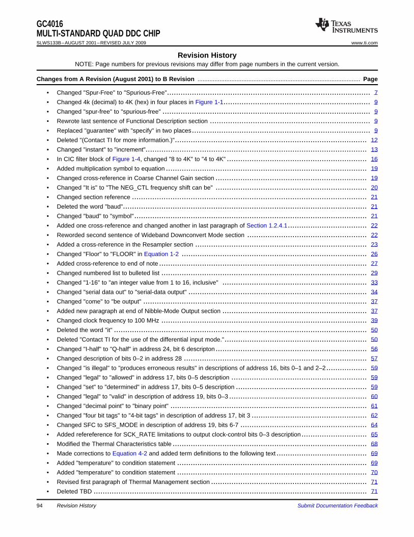
Revision History
GC4016MULTI-STANDARD QUAD DDC CHIPSLWS133B–AUGUST 2001–REVISED JULY 2009 www.ti.com
NOTE: Page numbers for previous revisions may differ from page numbers in the current version.
Changes from A Revision (August 2001) to B Revision ................................................................................................ Page
• Changed "Spur-Free" to "Spurious-Free".......................................................................................... 7• Changed 4k (decimal) to 4K (hex) in four places in Figure 1-1................................................................. 9• Changed "spur-free" to "spurious-free" ............................................................................................ 9• Rewrote last sentence of Functional Description section ....................................................................... 9• Replaced "guarantee" with "specify" in two places............................................................................... 9• Deleted "(Contact TI for more information.)"..................................................................................... 12• Changed "instant" to "increment".................................................................................................. 13• In CIC filter block of Figure 1-4, changed "8 to 4K" to "4 to 4K" .............................................................. 16• Added multiplication symbol to equation ......................................................................................... 19• Changed cross-reference in Coarse Channel Gain section ................................................................... 19• Changed "It is" to "The NEG_CTL frequency shift can be" ................................................................... 20• Changed section reference ........................................................................................................ 21• Deleted the word "baud"............................................................................................................ 21• Changed "baud" to "symbol"....................................................................................................... 21• Added one cross-reference and changed another in last paragraph of Section 1.2.4.1................................... 22• Reworded second sentence of Wideband Downconvert Mode section ..................................................... 22• Added a cross-reference in the Resampler section ............................................................................ 23• Changed "Floor" to "FLOOR" in Equation 1-2 .................................................................................. 26• Added cross-reference to end of note ............................................................................................ 27• Changed numbered list to bulleted list ........................................................................................... 29• Changed "1-16" to "an integer value from 1 to 16, inclusive" ................................................................ 33• Changed "serial data out" to "serial-data output" ............................................................................... 34• Changed "come" to "be output" ................................................................................................... 37• Added new paragraph at end of Nibble-Mode Output section ................................................................ 37• Changed clock frequency to 100 MHz ........................................................................................... 39• Deleted the word "it" ................................................................................................................ 50• Deleted "Contact TI for the use of the differential input mode."............................................................... 50• Changed "I-half" to "Q-half" in address 24, bit 6 descripton ................................................................... 56• Changed description of bits 0–2 in address 28 ................................................................................. 57• Changed "is illegal" to "produces erroneous results" in descriptions of address 16, bits 0–1 and 2–2.................. 59• Changed "legal" to "allowed" in address 17, bits 0–5 description ............................................................ 59• Changed "set" to "determined" in address 17, bits 0–5 description .......................................................... 59• Changed "legal" to "valid" in description of address 19, bits 0–3 ............................................................. 60• Changed "decimal point" to "binary point" ....................................................................................... 61• Changed "four bit tags" to "4-bit tags" in description of address 17, bit 3 ................................................... 62• Changed SFC to SFS_MODE in description of address 19, bits 6-7 ........................................................ 64• Added refereference for SCK_RATE limitations to output clock-control bits 0–3 description............................. 65• Modified the Thermal Characteristics table ...................................................................................... 68• Made corrections to Equation 4-2 and added term definitions to the following text ........................................ 69• Added "temperature" to condition statement .................................................................................... 69• Added "temperature" to condition statement .................................................................................... 70• Revised first paragraph of Thermal Management section ..................................................................... 71• Deleted TBD ......................................................................................................................... 71
Revision History94 Submit Documentation Feedback
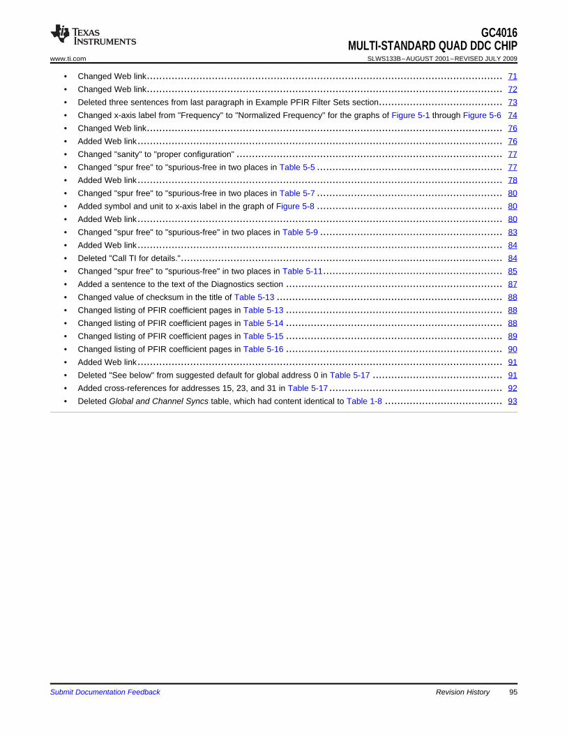
GC4016MULTI-STANDARD QUAD DDC CHIP
www.ti.com SLWS133B–AUGUST 2001–REVISED JULY 2009
• Changed Web link................................................................................................................... 71• Changed Web link................................................................................................................... 72• Deleted three sentences from last paragraph in Example PFIR Filter Sets section........................................ 73• Changed x-axis label from "Frequency" to "Normalized Frequency" for the graphs of Figure 5-1 through Figure 5-6 74• Changed Web link................................................................................................................... 76• Added Web link...................................................................................................................... 76• Changed "sanity" to "proper configuration" ...................................................................................... 77• Changed "spur free" to "spurious-free in two places in Table 5-5 ............................................................ 77• Added Web link...................................................................................................................... 78• Changed "spur free" to "spurious-free in two places in Table 5-7 ............................................................ 80• Added symbol and unit to x-axis label in the graph of Figure 5-8 ............................................................ 80• Added Web link...................................................................................................................... 80• Changed "spur free" to "spurious-free" in two places in Table 5-9 ........................................................... 83• Added Web link...................................................................................................................... 84• Deleted "Call TI for details."........................................................................................................ 84• Changed "spur free" to "spurious-free" in two places in Table 5-11.......................................................... 85• Added a sentence to the text of the Diagnostics section ...................................................................... 87• Changed value of checksum in the title of Table 5-13 ......................................................................... 88• Changed listing of PFIR coefficient pages in Table 5-13 ...................................................................... 88• Changed listing of PFIR coefficient pages in Table 5-14 ...................................................................... 88• Changed listing of PFIR coefficient pages in Table 5-15 ...................................................................... 89• Changed listing of PFIR coefficient pages in Table 5-16 ...................................................................... 90• Added Web link...................................................................................................................... 91• Deleted "See below" from suggested default for global address 0 in Table 5-17 .......................................... 91• Added cross-references for addresses 15, 23, and 31 in Table 5-17 ........................................................ 92• Deleted Global and Channel Syncs table, which had content identical to Table 1-8 ...................................... 93
Submit Documentation Feedback Revision History 95

PACKAGE OPTION ADDENDUM
www.ti.com 24-Jun-2015
Addendum-Page 1
PACKAGING INFORMATION
Orderable Device Status(1)
Package Type PackageDrawing
Pins PackageQty
Eco Plan(2)
Lead/Ball Finish(6)
MSL Peak Temp(3)
Op Temp (°C) Device Marking(4/5)
Samples
GC4016-PB LIFEBUY BGA GJZ 160 126 TBD SNPB Level-3-220C-168 HR GC4016PBQUAD DDC
GC4016-PBZ LIFEBUY BGA ZJZ 160 126 Green (RoHS& no Sb/Br)
SNAGCU Level-3-260C-168 HR -40 to 85 GC4016PBZQUAD DDC
(1) The marketing status values are defined as follows:ACTIVE: Product device recommended for new designs.LIFEBUY: TI has announced that the device will be discontinued, and a lifetime-buy period is in effect.NRND: Not recommended for new designs. Device is in production to support existing customers, but TI does not recommend using this part in a new design.PREVIEW: Device has been announced but is not in production. Samples may or may not be available.OBSOLETE: TI has discontinued the production of the device.
(2) Eco Plan - The planned eco-friendly classification: Pb-Free (RoHS), Pb-Free (RoHS Exempt), or Green (RoHS & no Sb/Br) - please check http://www.ti.com/productcontent for the latest availabilityinformation and additional product content details.TBD: The Pb-Free/Green conversion plan has not been defined.Pb-Free (RoHS): TI's terms "Lead-Free" or "Pb-Free" mean semiconductor products that are compatible with the current RoHS requirements for all 6 substances, including the requirement thatlead not exceed 0.1% by weight in homogeneous materials. Where designed to be soldered at high temperatures, TI Pb-Free products are suitable for use in specified lead-free processes.Pb-Free (RoHS Exempt): This component has a RoHS exemption for either 1) lead-based flip-chip solder bumps used between the die and package, or 2) lead-based die adhesive used betweenthe die and leadframe. The component is otherwise considered Pb-Free (RoHS compatible) as defined above.Green (RoHS & no Sb/Br): TI defines "Green" to mean Pb-Free (RoHS compatible), and free of Bromine (Br) and Antimony (Sb) based flame retardants (Br or Sb do not exceed 0.1% by weightin homogeneous material)
(3) MSL, Peak Temp. - The Moisture Sensitivity Level rating according to the JEDEC industry standard classifications, and peak solder temperature.
(4) There may be additional marking, which relates to the logo, the lot trace code information, or the environmental category on the device.
(5) Multiple Device Markings will be inside parentheses. Only one Device Marking contained in parentheses and separated by a "~" will appear on a device. If a line is indented then it is a continuationof the previous line and the two combined represent the entire Device Marking for that device.
(6) Lead/Ball Finish - Orderable Devices may have multiple material finish options. Finish options are separated by a vertical ruled line. Lead/Ball Finish values may wrap to two lines if the finishvalue exceeds the maximum column width.
Important Information and Disclaimer:The information provided on this page represents TI's knowledge and belief as of the date that it is provided. TI bases its knowledge and belief on informationprovided by third parties, and makes no representation or warranty as to the accuracy of such information. Efforts are underway to better integrate information from third parties. TI has taken andcontinues to take reasonable steps to provide representative and accurate information but may not have conducted destructive testing or chemical analysis on incoming materials and chemicals.TI and TI suppliers consider certain information to be proprietary, and thus CAS numbers and other limited information may not be available for release.

PACKAGE OPTION ADDENDUM
www.ti.com 24-Jun-2015
Addendum-Page 2
In no event shall TI's liability arising out of such information exceed the total purchase price of the TI part(s) at issue in this document sold by TI to Customer on an annual basis.


IMPORTANT NOTICE
Texas Instruments Incorporated and its subsidiaries (TI) reserve the right to make corrections, enhancements, improvements and otherchanges to its semiconductor products and services per JESD46, latest issue, and to discontinue any product or service per JESD48, latestissue. Buyers should obtain the latest relevant information before placing orders and should verify that such information is current andcomplete. All semiconductor products (also referred to herein as “components”) are sold subject to TI’s terms and conditions of salesupplied at the time of order acknowledgment.TI warrants performance of its components to the specifications applicable at the time of sale, in accordance with the warranty in TI’s termsand conditions of sale of semiconductor products. Testing and other quality control techniques are used to the extent TI deems necessaryto support this warranty. Except where mandated by applicable law, testing of all parameters of each component is not necessarilyperformed.TI assumes no liability for applications assistance or the design of Buyers’ products. Buyers are responsible for their products andapplications using TI components. To minimize the risks associated with Buyers’ products and applications, Buyers should provideadequate design and operating safeguards.TI does not warrant or represent that any license, either express or implied, is granted under any patent right, copyright, mask work right, orother intellectual property right relating to any combination, machine, or process in which TI components or services are used. Informationpublished by TI regarding third-party products or services does not constitute a license to use such products or services or a warranty orendorsement thereof. Use of such information may require a license from a third party under the patents or other intellectual property of thethird party, or a license from TI under the patents or other intellectual property of TI.Reproduction of significant portions of TI information in TI data books or data sheets is permissible only if reproduction is without alterationand is accompanied by all associated warranties, conditions, limitations, and notices. TI is not responsible or liable for such altereddocumentation. Information of third parties may be subject to additional restrictions.Resale of TI components or services with statements different from or beyond the parameters stated by TI for that component or servicevoids all express and any implied warranties for the associated TI component or service and is an unfair and deceptive business practice.TI is not responsible or liable for any such statements.Buyer acknowledges and agrees that it is solely responsible for compliance with all legal, regulatory and safety-related requirementsconcerning its products, and any use of TI components in its applications, notwithstanding any applications-related information or supportthat may be provided by TI. Buyer represents and agrees that it has all the necessary expertise to create and implement safeguards whichanticipate dangerous consequences of failures, monitor failures and their consequences, lessen the likelihood of failures that might causeharm and take appropriate remedial actions. Buyer will fully indemnify TI and its representatives against any damages arising out of the useof any TI components in safety-critical applications.In some cases, TI components may be promoted specifically to facilitate safety-related applications. With such components, TI’s goal is tohelp enable customers to design and create their own end-product solutions that meet applicable functional safety standards andrequirements. Nonetheless, such components are subject to these terms.No TI components are authorized for use in FDA Class III (or similar life-critical medical equipment) unless authorized officers of the partieshave executed a special agreement specifically governing such use.Only those TI components which TI has specifically designated as military grade or “enhanced plastic” are designed and intended for use inmilitary/aerospace applications or environments. Buyer acknowledges and agrees that any military or aerospace use of TI componentswhich have not been so designated is solely at the Buyer's risk, and that Buyer is solely responsible for compliance with all legal andregulatory requirements in connection with such use.TI has specifically designated certain components as meeting ISO/TS16949 requirements, mainly for automotive use. In any case of use ofnon-designated products, TI will not be responsible for any failure to meet ISO/TS16949.
Products ApplicationsAudio www.ti.com/audio Automotive and Transportation www.ti.com/automotiveAmplifiers amplifier.ti.com Communications and Telecom www.ti.com/communicationsData Converters dataconverter.ti.com Computers and Peripherals www.ti.com/computersDLP® Products www.dlp.com Consumer Electronics www.ti.com/consumer-appsDSP dsp.ti.com Energy and Lighting www.ti.com/energyClocks and Timers www.ti.com/clocks Industrial www.ti.com/industrialInterface interface.ti.com Medical www.ti.com/medicalLogic logic.ti.com Security www.ti.com/securityPower Mgmt power.ti.com Space, Avionics and Defense www.ti.com/space-avionics-defenseMicrocontrollers microcontroller.ti.com Video and Imaging www.ti.com/videoRFID www.ti-rfid.comOMAP Applications Processors www.ti.com/omap TI E2E Community e2e.ti.comWireless Connectivity www.ti.com/wirelessconnectivity
Mailing Address: Texas Instruments, Post Office Box 655303, Dallas, Texas 75265Copyright © 2015, Texas Instruments Incorporated