
MTTC PRESSURE SENSOR OVERVIEW - SCME - Southwest Center
14
MTTC PRESSURE SENSOR OVERVIEW Process Introduction
Transcript of MTTC PRESSURE SENSOR OVERVIEW - SCME - Southwest Center

MTTC PRESSURE SENSOR
OVERVIEW
Process Introduction

Pressure Sensor
Process developed at the
UNM MTTC/CNM
Design incorporates a
Wheatstone bridge as an
electronic sensing circuit
4 Resistors (2 fixed, 2
variable)
Conducting metal is gold
4 pads as leads

Finding Change in Pressure
A thin membrane of silicon nitride is the
sensing membrane
Cavity acting as reference pressure
Membrane stretches when pressure on
opposite sides of the membrane are
different.
As the membrane deflects, the resistance
will change in the variable resistors
As the pressure changes, the resistance
changes due to change in length
A calibration curve is created using known
pressure differences and resistance values

Pressure Sensor Features
Wheatstone bridge electronic sensing circuit
Deposit metal (chrome/gold)
Sensing Membrane
Silicon Nitride
Reference chamber
Etch away a hole to act as the chamber

How do we make it?
MTTC Pressure Sensor Process uses 2 micromaching
process techniques
Surface micromachining
Bulk micromachining
Wheatstone bridge electronic sensing circuit
Deposit metal (chrome/gold)
Surface micromachining techniques
Sensing Membrane
Deposit Silicon Nitride thin film
Surface micromachining techniques
Reference chamber
Etch away a hole to act as the chamber
Bulk micromachining techniques
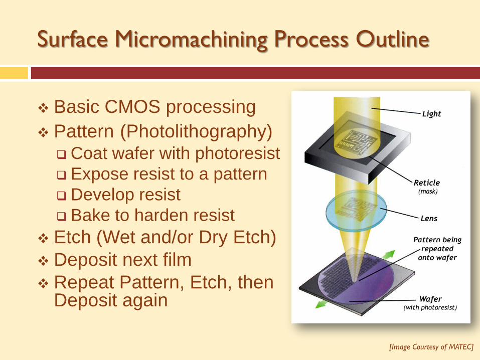
Surface Micromachining Process Outline
Basic CMOS processing
Pattern (Photolithography)Coat wafer with photoresist
Expose resist to a pattern
Develop resist
Bake to harden resist
Etch (Wet and/or Dry Etch)
Deposit next film
Repeat Pattern, Etch, then Deposit again
[Image Courtesy of MATEC]
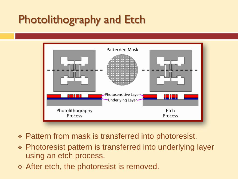
Photolithography and Etch
Pattern from mask is transferred into photoresist.
Photoresist pattern is transferred into underlying layer using an etch process.
After etch, the photoresist is removed.

Bulk Micromachining
Bulk micromachining defines structures by selectively etching inside a substrate, usually by removing the “bulk” of a material.
This is a subtractive process.
Take for example the cliff dwellings at Mesa Verde which were formed below the surface of the flat topped mesa. Man and nature have “bulk etched” these dwellings into the side of the cliff.
Micro-machined structures are formed into the wafer substrate in the same manner.
[Image printed with permission from Barb Lopez]

Bulk Micromachining
Monocrystalline silicon wafers
are mostly etched to form
three-dimensional MEMS
devices.
The silicon in the wafer
substrate is specifically
removed using anisotropic
chemistries.
Sensors such as piezoresistive
pressure sensors have been
manufactured in high volume.
Bulk micromachined devices
typically have high aspect
ratios.
Backside of MTTC Pressure Sensor
(100)
(111)
Silicon nitride

Bulk Micromachining
Bulk Micromachining involves deposition, patterning and etching of structural and sacrificial layers.
It also includes bulk dry or wet etching of relatively large amounts of silicon substrate.
Structures include high aspect ratio fluidic channels, alignment grooves, pits.
[Image courtesy of
Khalil Najafi,
University of
Michigan]
MEMS pressure sensor
(frontside/backside) [Images
courtesy of MTTC/UNM]

Bulk Micromachining
For silicon wafers, silicon dioxide
or nitride are most commonly
used as an etch mask. The film is
then patterned to allow the
removal of undesired portions of
the film.
A Silicon Nitride etch mask on
the backside of a wafer used
for pressure sensors. A
subsequent etch process
anisotropically removes the
bulk silicon not protected by the
nitride mask.
Anisotropic Isotropic
Slow etching
crystal planeEtch Mask

Bulk Micromachining –Wet and Dry Etch
Two types of etching
can be used in Bulk
Micromachining
Wet Etch
Dry Etch
Both wet and dry etch
can produce either
Isotropic Etch
Anisotropic Etch
Etch profiles will be
different depending
upon type of etch and
the etchant

Bulk Micromachining –Wet Etchants
Chemicals are used to anisotropically etch crystalline substrates
Potassium Hydroxide (KOH)
Ethylene Diamine Pyrocatechol (EDP)
Tetramethyl Ammonium Hydroxide (TMAH)
Sodium Hydroxide (NaOH)
N2H4-H2O (Hydrazine)

14
The MTTC Pressure Sensor process uses a gold Wheatstone
bridge electronic sensing circuit and a silicon nitride
membrane. The reference chamber is created using an
anisotropic etch which removes the bulk of the silicon on the
backside of the wafer. The manufacture of these features
require both surface micromachining and bulk
micromachining techniques.
Summary