
MT3337 All-in-One GNSS Datasheet · 2017-04-20 · MT3337 All-in-One GPS Datasheet Version: 1.0...
31
MT3337 All-in-One GPS Datasheet Version: 1.0 Release date: 13 January 2017 © 2016 MediaTek Inc. This document contains information that is proprietary to MediaTek Inc. (“MediaTek”) and/or its licensor(s). MediaTek cannot grant you permission for any material that is owned by third parties. You may only use or reproduce this document if you have agreed to and been bound by the applicable license agreement with MediaTek (“License Agreement”) and been granted explicit permission within the License Agreement (“Permitted User”). If you are not a Permitted User, please cease any access or use of this document immediately. Any unauthorized use, reproduction or disclosure of this document in whole or in part is strictly prohibited. THIS DOCUMENT IS PROVIDED ON AN “AS-IS” BASIS ONLY. MEDIATEK EXPRESSLY DISCLAIMS ANY AND ALL WARRANTIES OF ANY KIND AND SHALL IN NO EVENT BE LIABLE FOR ANY CLAIMS RELATING TO OR ARISING OUT OF THIS DOCUMENT OR ANY USE OR INABILITY TO USE THEREOF. Specifications contained herein are subject to change without notice.
Transcript of MT3337 All-in-One GNSS Datasheet · 2017-04-20 · MT3337 All-in-One GPS Datasheet Version: 1.0...

MT3337 All-in-One GPS Datasheet
Version: 1.0
Release date: 13 January 2017
© 2016 MediaTek Inc.
This document contains information that is proprietary to MediaTek Inc. (“MediaTek”) and/or its licensor(s). MediaTek cannot grant you permission for any material that is owned by third parties. You may only use or reproduce this document if you have agreed to and been bound by the applicable license agreement with MediaTek (“License Agreement”) and been granted explicit permission within the License Agreement (“Permitted User”). If you are not a Permitted User, please cease any access or use of this document immediately. Any unauthorized use, reproduction or disclosure of this document in whole or in part is strictly prohibited. THIS DOCUMENT IS PROVIDED ON AN “AS-IS” BASIS ONLY. MEDIATEK EXPRESSLY DISCLAIMS ANY AND ALL WARRANTIES OF ANY KIND AND SHALL IN NO EVENT BE LIABLE FOR ANY CLAIMS RELATING TO OR ARISING OUT OF THIS DOCUMENT OR ANY USE OR INABILITY TO USE THEREOF. Specifications contained herein are subject to change without notice.
MT3337 All-in-One GNSS Datasheet
© 2016 MediaTek Inc. Page 2 of 31 This document contains information that is proprietary to MediaTek Inc. (“MediaTek”) and/or its licensor(s). Any unauthorized use, reproduction or disclosure of this document in whole or in part is strictly prohibited.
Document Revision History
Revision Date Description 1.0 13 January 2017 Initial release

MT3337 All-in-One GNSS Datasheet
© 2016 MediaTek Inc. Page 3 of 31 This document contains information that is proprietary to MediaTek Inc. (“MediaTek”) and/or its licensor(s). Any unauthorized use, reproduction or disclosure of this document in whole or in part is strictly prohibited.
Table of Contents
1. Introduction ........................................................................................................................................ 6 1.1. Overview ............................................................................................................................................ 6 1.2. Features .............................................................................................................................................. 7
2. Pin Assignment and Description .......................................................................................................... 8 2.1. 8 2.2. Pin descriptions (top view) ................................................................................................................. 8 2.3. Pin descriptions .................................................................................................................................. 8
3. System Block Diagrams ..................................................................................................................... 11 3.1. Single-chip receiver architecture ..................................................................................................... 11 3.2. Functional block diagram (RF subsystem) ........................................................................................ 11
4. Radio Subsystem Features ................................................................................................................ 12 4.1. Low Noise Amplifier (LNA) and mixer .............................................................................................. 12 4.2. Voltage Controlled Oscillator (VCO) and synthesizer ....................................................................... 12 4.3. Intermediate frequency (IF) channel select filter (CSF) .................................................................... 12 4.4. Programmable Gain Amplifier (PGA) ............................................................................................... 12 4.5. Analog-to-Digital Converter (ADC) ................................................................................................... 12
5. Processor Subsystem Features .......................................................................................................... 13 5.1. ARM7EJ-S ......................................................................................................................................... 13 5.2. Battery backed-up memory ............................................................................................................. 13 5.3. Switching Mode Power Supply (SMPS) ............................................................................................ 14 5.4. Timer function .................................................................................................................................. 14 5.5. General Purpose Input/Output (GPIO) in the RTC domain .............................................................. 14 5.6. Low power detection ....................................................................................................................... 14 5.7. Clock module .................................................................................................................................... 14 5.8. Reset controller ................................................................................................................................ 14 5.9. Serial interface ................................................................................................................................. 15
5.9.1. Universal Asynchronous Receiver/Transmitter (UART) ................................................. 15 5.10. Interrupt control unit ....................................................................................................................... 16 5.11. eFuse ................................................................................................................................................ 16 5.12. GPIO unit .......................................................................................................................................... 16 5.13. Pulse Per Second (PPS) ..................................................................................................................... 16 5.14. PPS Sync NMEA ................................................................................................................................ 16 5.15. Power schemes ................................................................................................................................ 16
6. Electrical Characteristics .................................................................................................................... 20 6.1. DC characteristics ............................................................................................................................. 20
6.1.1. Absolute maximum ratings ............................................................................................ 20 6.1.2. Recommended operating conditions ............................................................................. 20 6.1.3. General DC characteristics ............................................................................................. 21 6.1.4. DC electrical characteristics for 2.8 volts operation ....................................................... 21 6.1.5. DC electrical characteristics for 1.8 volts operation ....................................................... 21 6.1.6. DC electrical characteristics for 1.2 volts operation (for TIMER and 32K_OUT) ............ 21
6.2. Analog characteristics ...................................................................................................................... 22 6.2.1. SMPS DC characteristics ................................................................................................. 22 6.2.2. TCXO LDO DC characteristics .......................................................................................... 22 6.2.3. TCXO SWITCH DC characteristics .................................................................................... 22 6.2.4. 1.2 volts core LDO DC characteristics ............................................................................. 23 6.2.5. 1.2 volts RTC LDO DC characteristics .............................................................................. 23

MT3337 All-in-One GNSS Datasheet
© 2016 MediaTek Inc. Page 4 of 31 This document contains information that is proprietary to MediaTek Inc. (“MediaTek”) and/or its licensor(s). Any unauthorized use, reproduction or disclosure of this document in whole or in part is strictly prohibited.
6.2.6. 32 kHz crystal oscillator (XOSC32) .................................................................................. 23 6.3. RF characteristics ............................................................................................................................. 23
6.3.1. DC electrical characteristics for RF subsystem ............................................................... 23 6.3.2. RX chain from LNA to PGA, before ADC ......................................................................... 24 6.3.3. Receiver front-end part (LNA only) ................................................................................ 24 6.3.4. Mixer and channel selection filter (CSF) ......................................................................... 24 6.3.5. Programmable gain amplifier (PGA) ............................................................................... 25 6.3.6. 2-bit and 4-bit quantizer (ADC) ...................................................................................... 25 6.3.7. Integrated synthesizer .................................................................................................... 25 6.3.8. Crystal oscillator (XO) ..................................................................................................... 25
7. Interface Characteristics .................................................................................................................... 26 7.1. JTAG interface timing ....................................................................................................................... 26 7.2. RS-232 interface timing .................................................................................................................... 26
8. Package Description .......................................................................................................................... 28 8.1. Ordering information ....................................................................................................................... 28 8.2. Top mark .......................................................................................................................................... 28 8.3. Package dimensions ......................................................................................................................... 29

MT3337 All-in-One GNSS Datasheet
© 2016 MediaTek Inc. Page 5 of 31 This document contains information that is proprietary to MediaTek Inc. (“MediaTek”) and/or its licensor(s). Any unauthorized use, reproduction or disclosure of this document in whole or in part is strictly prohibited.
Lists of figures
Figure 3-1: MT3337 system block diagram ........................................................................................................... 11 Figure 3-2: MT3337 RF functional block diagram ................................................................................................. 11 Figure 5-1: RTC with internal RTC LDO application circuit 1 ................................................................................. 13 Figure 5-2: RTC with internal RTC LDO application circuit 2 ................................................................................. 13 Figure 5-3: Power on reset diagram ..................................................................................................................... 15 Figure 5-4: Power on/off reset behavior .............................................................................................................. 15 Figure 5-5: NMEA output timing relation with PPS Signal .................................................................................... 16 Figure 5-6: Power supply connection (low power) ............................................................................................... 17 Figure 5-7: Power supply connection (low cost) .................................................................................................. 18 Figure 5-8: Power supply connection (external LDO) ........................................................................................... 18 Figure 7-1: Timing diagram of JTAG interface ...................................................................................................... 26 Figure 7-2: Timing diagram of RS-232 interface ................................................................................................... 27

MT3337 All-in-One GNSS Datasheet
© 2016 MediaTek Inc. Page 6 of 31 This document contains information that is proprietary to MediaTek Inc. (“MediaTek”) and/or its licensor(s). Any unauthorized use, reproduction or disclosure of this document in whole or in part is strictly prohibited.
1. Introduction
1.1. Overview
MediaTek MT3337 is a high-performance single-chip GPS solution that includes on-chip CMOS RF, digital baseband, and ARM7 CPU. It’s able to achieve the industry’s highest level of sensitivity, accuracy and Time-to-First-Fix (TTFF) with the lowest power consumption. Its small footprint lead-free package and minimal additional BOM requirements provide significant reductions in the design, manufacturing and testing resources required to create devices. The main features that help reduce device BOM are:
• Built-in Low Noise Amplifier (LNA) that eliminates the need for an external antenna.
• Built-in image-rejection mixer that removes the need for an external Surface Acoustic Wave (SAW) filter.
• Built-in automatic center frequency calibration band pass filter that means an external filter is not required.
• Built-in power management that enables MT3337 to be easily integrated into your system without an extra voltage regulator. With both linear and highly efficient switching type regulators embedded, MT3337 supports direct battery connection and doesn’t need an external low-dropout (LDO) regulator, which offers flexibility in circuit design.
In addition, 12 multi-tone active interference cancellers (ISSCC2011 award) can eliminate the need to design interference cancelation, simplifying PCB design. The integrated Phase-Locked Loop (PLL) with Voltage Controlled Oscillator (VCO) provides excellent phase noise performance and fast locking times. A battery backed-up memory and a real-time clock are also provided to accelerate location acquisition at system restart.
MT3337 supports up to 210 PRN channels. With 66 search channels and 22 simultaneous tracking channels, MT3337 acquires and tracks satellites in the shortest time even at indoor signal levels. MT3337 supports various location and navigation applications, including autonomous GPS, QZSS, DGPS (RTCM) and A-GPS. MT3337 supports EASYTM (Embedded Assisted System) Self-Generated Orbit Prediction feature. In comparison to EPO, Hot Still or A-GPS, it provides up to 3 days GPS orbit prediction ability without any host CPU porting or internet connection requirement.
The excellent low-power consumption characteristics of MT3333 (25 mW for acquisition and 18 mW for tracking) means that — without changing the specified battery — power sensitive devices, especially portable applications, will be able to offer device users longer operating times. Combined with advanced software features including EASY™, EPO™ and LOCUS™, MT3337 provides always-on positioning with minimal average power consumption. These great features provide outstanding performance for portable applications, such as DSC, mobile phones, PMP and gaming devices.

MT3337 All-in-One GNSS Datasheet
© 2016 MediaTek Inc. Page 7 of 31 This document contains information that is proprietary to MediaTek Inc. (“MediaTek”) and/or its licensor(s). Any unauthorized use, reproduction or disclosure of this document in whole or in part is strictly prohibited.
1.2. Features
• Specifications o 22 tracking / 66 acquisition-channel GPS
receiver o Supports up to 210 PRN channels o Supports GPS including QZSS o Supports WAAS/EGNOS/MSAS/GAGAN o 12 multi-tone active interference
cancellers (ISSCC2011 award) o RTCM ready o Indoor and outdoor multi-path detection
and compensation o Supports FCC E911 compliance and A-
GPS o Maximum fixed update rate up to 5 Hz
• Advanced software features o EPO™ orbit prediction o EASY™ self-generated orbit prediction o Supports time service application, which
is achieved by the PPS synced with the NMEA feature.
• Reference oscillator o TCXO
Frequency: 16.368 MHz, 26 MHz Frequency variation: ±2.0 ppm
• RF configuration o 4-bit IF signal o SOC, integrated in single chip with CMOS
process • ARM7EJ-S CPU
o Up to 98 MHz processor clock o Dynamic clock rate control
• Pulse-per-second (PPS) GPS time reference o Adjustable duty cycle o Typical accuracy: ±10 ns
• Power scheme o Built-in 1.8 volts Switching Mode Power
Supply (SMPS) o Direct lithium battery connection (2.8 ~ 4.3
volts) o Built-in 1.2 volts RTC LDO, 1.2 volts core
LDO and 2.8 volts TCXO LDO • Build-in reset controller
o Does not need of external reset control IC • Internal real-time clock (RTC)
o 32.768 kHz ± 20 ppm crystal o Timer pin for external device on/off control o 1.2 volts RTC clock output
• Serial interface o UART : 4800/9600/38400/115200 bps o GPIO interface (up to 16 pins)
• NMEA
o NMEA 0183 standard V3.01 and backward compliance
o Supports 219 different datum’s • Sensitivity
o Acquisition: -148 dBm (cold) / -163 dBm (hot)
o Tracking: -165 dBm • Ultra-low power consumption
o Acquisition: 25 mW o Tracking: 18 mW
• Packagee
o VFBGA: 4.3 mm x 4.3 mm, 57 balls, 0.5 mm pitch
• Slim hardware design o Mimimun solution footprint of 52 mm2
M

MT3337 All-in-One GNSS Datasheet
© 2016 MediaTek Inc. Page 8 of 31 This document contains information that is proprietary to MediaTek Inc. (“MediaTek”) and/or its licensor(s). Any unauthorized use, reproduction or disclosure of this document in whole or in part is strictly prohibited.
2. Pin Assignment and Description
2.2. Pin descriptions (top view)
1 2 3 4 5 6 7 8
A RFIN AVSS_HF EXT_R HRST_B DVDD_CORE2
SCS1_ GIO11 NC
B AVDD_RFCORE
AVSS_VCO RFTEST XTEST DVDD_IO2 GIO9 RX0 TX0
C AVDD_BGXOTHLS
AVSS_LF NC EINT0 EINT1 GIO7 EINT2 RX2
D OSC AVSS28_TLDO
NC NC DVSS_IO2 GIO10 SCK1 EINT3
E AVDD43_VBAT
AVDD28_CLDO
NC NC DVSS_CORE
GIO8 DVSS_IO1 DVDD_IO1
F VREF GND_MISC AVSS12_CLDO
BUCK_FB DVDD_CORE1
DVDD_IO3 TX2 FSOURCE_WR
G AVDD28_TLDO
AVDD28_TLDO_SW
PGND_SMPS
NC TIMER 32K_OUT GIO6 RX1
H AVDD12_CLDO
LXBK AVDD43_SMPS
RTCCLK_O RTCCLK AVDD43_RTC
AVDD12_RTC
TX1
2.3. Pin descriptions
Pin# Symbol Type Description System interface (2 pins)
A4 HRST_B 2.8V LVTTL input System reset. Active low. B4 XTEST 2.8V LVTTL input Test mode. Must keep low in normal mode.
Peripheral interface (8 pins) B7 RX0 2.8V, LVTTL I/O Serial input for UART 0 B8 TX0 2.8V, LVTTL I/O
PPU, PPD, SMT 4mA, 8mA, 12mA, 16mA PDR
Serial output for UART 0 Default: pull-up Default: 8mA driving
G8 RX1 2.8V, LVTTL I/O Serial input for UART 1 H8 TX1 2.8V, LVTTL I/O Serial output for UART 1 C8 RX2 2.8V, LVTTL I/O Serial input for UART 2

MT3337 All-in-One GNSS Datasheet
© 2016 MediaTek Inc. Page 9 of 31 This document contains information that is proprietary to MediaTek Inc. (“MediaTek”) and/or its licensor(s). Any unauthorized use, reproduction or disclosure of this document in whole or in part is strictly prohibited.
Pin# Symbol Type Description F7 TX2 2.8V, LVTTL I/O Serial output for UART 2 D7 SCK1 2.8V, LVTTL I/O SPI clock output A6 SCS1_ 2.8V, LVTTL I/O SPI slave selection 1
Debugging interface (6 pins) G7 GIO6 2.8V, LVTTL I/O GPIO C6 GIO7 2.8V, LVTTL I/O GPIO E6 GIO8 2.8V, LVTTL I/O GPIO B6 GIO9 2.8V, LVTTL I/O GPIO D6 GIO10 2.8V, LVTTL I/O GPIO A7 GIO11 2.8V, LVTTL I/O GPIO
External system interface (4 pins) C4 EINT0 2.8V, LVTTL I/O External interrupt 0 C5 EINT1 2.8V, LVTTL I/O External interrupt 1 C7 EINT2 2.8V, LVTTL I/O External interrupt 2 D8 EINT3 2.8V, LVTTL I/O External interrupt 3
RTC interface (6 pins) H6 AVDD43_RTC Analog power RTC LDO input H7 AVDD12_RTC Analog power RTC LDO output H5 RTCCLK Analog input RTC 32KHz XTAL input H4 RTCCLK_O Analog output RTC 32KHz XTAL output G6 32K_OUT 1.2V LVTTL I/O RTC domain GPIO pin, can be programmed
to 32KHz clock output, DR wake-up signal input, or low power detection indicator signal
G5 TIMER 1.2V LVTTL I/O open drain, SMT 4mA, 8mA, 12mA, 16mA PDR
Wake up other devices from RTC. If this pin is not used, tie it to the ground.
RF and analog B1 AVDDRF_CORE RF power 1.8V supply for RF core circuits A3 EXT_R Analog External R connection for R calibration B3 RFTEST Analog signal RF testing signal B2 AVSS_VCO RF ground GND pin for SX VCO C1 AVDD_BGXOTHLS RF power 1.8V supply for XTAL OSC, bandgap,
Thermal sensor and level shifter C2 AVSS_LF RF ground GND pin for low-frequency circuits D1 OSC Analog signal Input for crystal oscillator or TCXO A2 AVSS_HF RF ground GND pin for high-frequency circuits A1 RF_IN RF signal LNA RF Input pin F5 DVDD_CORE1 Digital power Digital 1.2V core power input A5 DVDD_CORE2 Digital power Digital 1.2V core power input E5 DVSS_CORE Digital ground Digital 1.2V core ground E8 DVDD_IO1 Digital power Digital 1.8/2.8V IO power input B5 DVDD_IO2 Digital power Digital 1.8/2.8V IO power input

MT3337 All-in-One GNSS Datasheet
© 2016 MediaTek Inc. Page 10 of 31 This document contains information that is proprietary to MediaTek Inc. (“MediaTek”) and/or its licensor(s). Any unauthorized use, reproduction or disclosure of this document in whole or in part is strictly prohibited.
Pin# Symbol Type Description F6 DVDD_IO3 Digital power Digital 1.8/2.8V IO power input E7 DVSS_IO1 Digital ground Digital 1.8/2.8V IO ground D5 DVSS_IO2 Digital ground Digital 1.8/2.8V IO ground F8 FSOURCE_WR Digital power EFUSE 2.8V write power supply F1 VREF Analog Bandgap output pin. Must add 1µF
decoupling cap on PCB. F2 GND_MISC Analog ground GND pin for buck controller D2 AVSS28_TLDO Analog ground GND pin for TCXO LDO and start-up block E1 AVDD43_VBAT Analog power TCXO LDO input pin. Always be powered by
external source. UVLO will detect this PIN to check power status.
G2 AVDD28_TLDO_SW Analog power TCXO power switch output pin G1 AVDD28_TLDO Analog power TCXO LDO output pin E2 AVDD28_CLDO Analog power Core LDO input pin. Always powered by
external source or SMPS H1 AVDD12_CLDO Analog power Core LDO output pin F3 AVSS12_CLDO Analog ground GND pin for core LDO G3 PGND_SMPS SMPS SMPS GND pin H2 LXBK SMPS SMPS output pin H3 AVDD43_SMPS SMPS SMPS input pin. F4 BUCK_FB SMPS SMPS feedback pin
Notes: PPU = Programmable pull-up PPD = Programmable pull-down PSR = Programmable slew rate PDR = Programmable driving
MT3337 All-in-One GNSS Datasheet
© 2016 MediaTek Inc. Page 11 of 31 This document contains information that is proprietary to MediaTek Inc. (“MediaTek”) and/or its licensor(s). Any unauthorized use, reproduction or disclosure of this document in whole or in part is strictly prohibited.
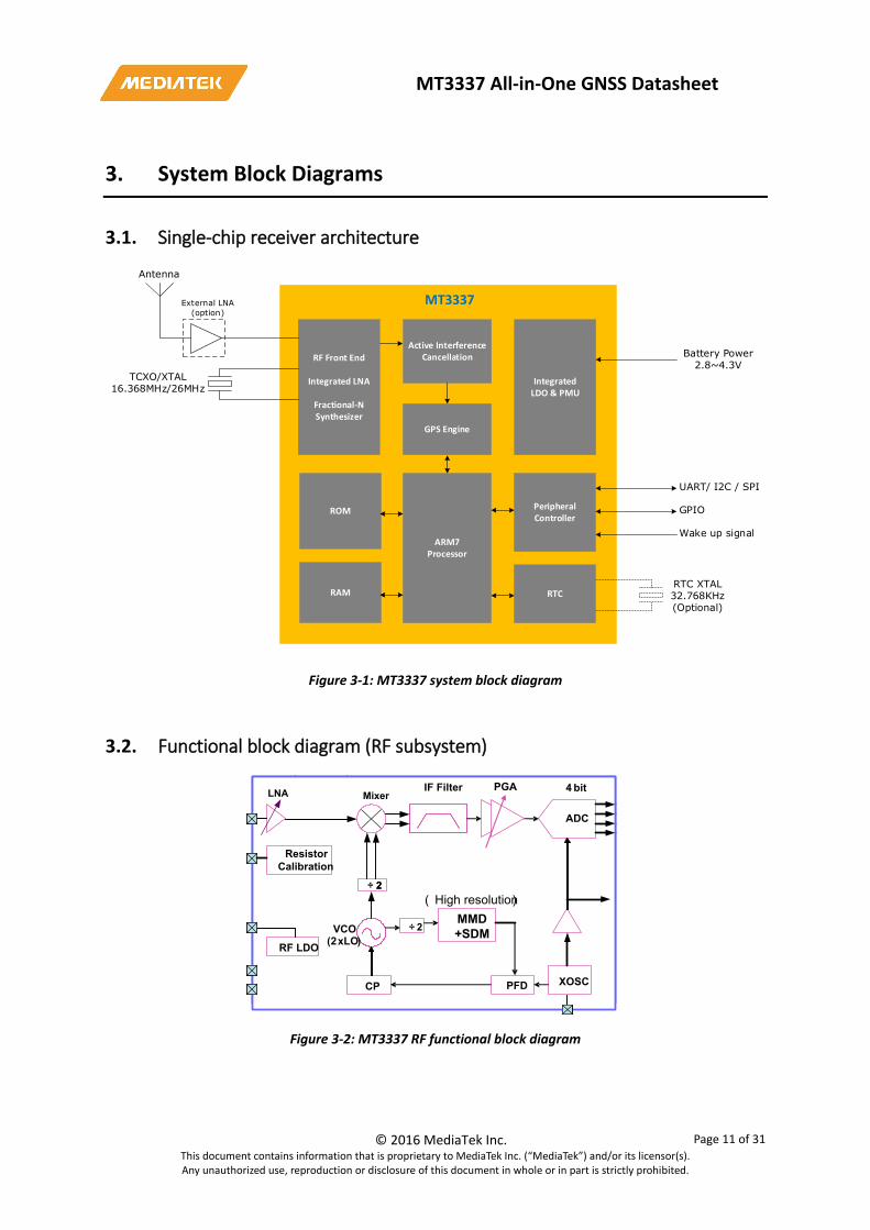
3. System Block Diagrams
3.1. Single-chip receiver architecture
RF Front End
Integrated LNA
Fractional-N Synthesizer
Peripheral Controller
RTC
ARM7Processor
Integrated LDO & PMU
RAM
ROM
UART/ I2C / SPI
Wake up signal
GPIO
Battery Power 2.8~4.3V
RTC XTAL32.768KHz(Optional)
External LNA(option)
Antenna
TCXO/XTAL16.368MHz/26MHz
MT3337
Active Interference Cancellation
GPS Engine
Figure 3-1: MT3337 system block diagram
3.2. Functional block diagram (RF subsystem)
ADC
Antenna Detector
PFDCP XOSC
LNAPGAIF Filter
VCO(2xLO)
4 bit
2 SDM
RF LDO
( High resolution )
(1.5 )
ADC
Resistor Calibration
PFDCP XOSC
LNA PGAIF Filter
VCO(2xLO)
4 bit
÷ 2MMD+SDM
RF LDO
( High resolution)2÷ 2
Mixer
Figure 3-2: MT3337 RF functional block diagram

MT3337 All-in-One GNSS Datasheet
© 2016 MediaTek Inc. Page 12 of 31 This document contains information that is proprietary to MediaTek Inc. (“MediaTek”) and/or its licensor(s). Any unauthorized use, reproduction or disclosure of this document in whole or in part is strictly prohibited.
4. Radio Subsystem Features
4.1. Low Noise Amplifier (LNA) and mixer
The LNA on MT3337 offers two antenna connectivity options:
• A GPS antenna connected directly to the internal LNA in high-gain mode, ideal for solutions without an external LNA.
• An external antenna and high gain external LNA connected to the internal LNA in low-gain mode, which offers high linearity. In this configuration, the external LNA gain ranging from 0 to 36 dB is recommended.
The down-conversion mixer down converts the amplified L1 band (1575.42 MHz) signal to a 4.092 MHz differential IF signal. In the application with external LNA, the external LNA gain ranging from 0 to 36 dB is recommended.
The down-conversion mixer is a single-ended passive mixer with current mode interface between the mixer and complex channel select filter (CSF).
4.2. Voltage Controlled Oscillator (VCO) and synthesizer
The frequency synthesizer includes a crystal oscillator, VCO, divider, phase frequency detector (PFD), charge pump (CP) and loop filter which are all integrated on the MT3337 chip. The VCO is auto-calibrated to its required sub-band, when the chip is powered on.
4.3. Intermediate frequency (IF) channel select filter (CSF)
The down converted IF signal from the mixer output passes through a bandpass CSF. Centered at 4.092 MHz, the filter rejects out-of-band (10 MHz) interferences by more than 20 dB and has a pass band ripple of less than 0.5 dB. The current-mode mixer and filter also provide a 32 dB pass band gain together to improve noise figure.
4.4. Programmable Gain Amplifier (PGA)
The PGA has approximately 40 dB of gain control range with approximately 1.6 dB per step. The maximum gain is around 40 dB. HPF circuits are implemented among PGAs to remove DC offset quickly.
4.5. Analog-to-Digital Converter (ADC)
The differential IF signal is quantized by a 4-bit ADC. The sampling clock can be provided from TCXO oscillator or using local oscillator with frequency divided by 96.

MT3337 All-in-One GNSS Datasheet
© 2016 MediaTek Inc. Page 13 of 31 This document contains information that is proprietary to MediaTek Inc. (“MediaTek”) and/or its licensor(s). Any unauthorized use, reproduction or disclosure of this document in whole or in part is strictly prohibited.
5. Processor Subsystem Features
5.1. ARM7EJ-S
The ARM7EJ-S processor provides the flexibility necessary to build Java-enabled, real-time embedded devices requiring small size, low-power and high performance. It builds on the features and benefits of the established ARM7TDMI core and is delivered in synthesizable form. ARM7EJ-S is supported by a wide variety of development tools and can run at speed up to 98 MHz.
ARM7EJ-S includes a JTAG interface that provides a standard development and debugging interface. The interface can connect to a variety of off-the-shelf emulators. The emulators provide single-step, trap and access to all the internal registers of the processor subsystem.
5.2. Battery backed-up memory
MT3337 provides very low leakage (about 5 µA in the backup mode) battery backed-up memory that contains the necessary GPS information for quick start-up and a small amount of user configuration variables. There is a built-in 1.2 volts LDO for the RTC domain and it can be bypassed while an external LDO is applied. The RTC LDO is a voltage regulator having very low quiescent current. The typical quiescent current is less than 2.5 µA. A small ceramic capacitor can be used as an output capacitor and the stable operation region ranges from very light load (~=0) to about 3 mA. The RTC LDO application circuits are shown in Figure 5-1 and Figure 5-2.
Figure 5-1: RTC with internal RTC LDO application circuit 1
Figure 5-2: RTC with internal RTC LDO application circuit 2

MT3337 All-in-One GNSS Datasheet
© 2016 MediaTek Inc. Page 14 of 31 This document contains information that is proprietary to MediaTek Inc. (“MediaTek”) and/or its licensor(s). Any unauthorized use, reproduction or disclosure of this document in whole or in part is strictly prohibited.
5.3. Switching Mode Power Supply (SMPS)
A built-in SMPS provides 1.8 volts power supply for the digital 1.2 volts Core Low-Dropout (CLDO) regulator and RF input power. In active mode, the SMPS operates in pulse width modulation (PWM) mode. In low power mode, the SMPS operates with reduced switching frequency in the pulse frequency modulation (PFM) mode. The recommended L/C value is 4.7 µH / 10 µF.
5.4. Timer function
The timer function supports a time tick generation of 31.25 ms resolution. With the 24-bit counter, the period of timer is from 31.25 ms to 524,287 s. The “PAD_TIMER” pin outputs 1’b0 signal during the timer period and becomes an input pin after timeout. The power control function for the system can be executed by connecting this pin to an external LDO controller and adding an external pull-high circuit.
5.5. General Purpose Input/Output (GPIO) in the RTC domain
The “32K_OUT” pin in the RTC domain can output 32.768 kHz clock. This can be used to support low clock rate operation mode, for applications or peripherals that need an external clock source. This pin can also be programmed to be the input pin to receive a wake-up signal from an external accelerator sensor IC, when MT3333 is in the low-power mode.
5.6. Low power detection
A low power detection circuit is implemented. Whenever the independent power source (AVDD12_RTC) becomes low voltage, the low power detection circuit will detect this condition and use an indicator signal at pin 32K_OUT (output high in normal condition and low in low-power condition) to reflect this condition.
5.7. Clock module
The clock module generates all internal clocks required by the processor, correlator, internal memory, bus interface and so on. The referenced input clock is generated from the RF subsystem. It also supports various power management modes.
5.8. Reset controller
The built-in reset controller generates reset signals for all digital blocks. It provides power-on reset and hardware trapping. The power-on reset level is at 2.7 ± 0.1 volts. The software reset function for different circuit blocks is also included. In Figure 5-4, the voltage drop time Tdrop_vbat and Tdrop_cldo depend on the capacitance connection of their power net. However, Tdrop_vbat > Tdrop_cldo should be guaranteed for the correct reset operation during power off sequence. It’s strongly recommended using external LDOs without output discharge function or ensure the Tdrop_vbat is greater than 100 ms.

MT3337 All-in-One GNSS Datasheet
© 2016 MediaTek Inc. Page 15 of 31 This document contains information that is proprietary to MediaTek Inc. (“MediaTek”) and/or its licensor(s). Any unauthorized use, reproduction or disclosure of this document in whole or in part is strictly prohibited.
Figure 5-3: Power on reset diagram
Figure 5-4: Power on/off reset behavior
5.9. Serial interface
MT3337 chipset firmware supports only one serial interface — UART.
5.9.1. Universal Asynchronous Receiver/Transmitter (UART)
MT3337 has three full duplex serial ports. UART converts bytes of data to and from asynchronous start-stop bit streams represented as binary electrical impulses.
UART communication functions provided include: UART data transmission/receive and NMEA sentences input/output. In general, UART0 is used for NMEA output and PMTK command input, while UART1 is RTCM input. You can adjust the UART2 port as desired. UART provides signal or message outputs.
The receiver (RX) and transmitter (TX) side of every port contains a 16-byte FIFO, but only UART0 has 256 bytes of URAM. The bit rates are adjustable and vary from 4800, 9600, 38400 and 115200 bps.

MT3337 All-in-One GNSS Datasheet
© 2016 MediaTek Inc. Page 16 of 31 This document contains information that is proprietary to MediaTek Inc. (“MediaTek”) and/or its licensor(s). Any unauthorized use, reproduction or disclosure of this document in whole or in part is strictly prohibited.
5.10. Interrupt control unit
The interrupt control unit manages all internal and external sources of interrupts, which include timer, watchdog, a serial UART interface and external user interrupt pins. These interrupt sources can be wake-up events when the chipset is in low power mode.
5.11. eFuse
eFuse is one of the One-Time-Programming (OTP) memories. The internal eFuse supports up to 128 bits for user configuration.
5.12. GPIO unit
MT3337 supports a variety of peripherals through up to 16 GPIO programmable ports. The unit manages all GPIO lines and supports a simple control interface. GPIO provides signal or message outputs.
5.13. Pulse Per Second (PPS)
The PPS signal is provided through the designated output pin for external applications. In addition to its limit of being active every second, it’s possible to set up the duration, frequency and active high/low by programming user-defined settings.
5.14. PPS Sync NMEA
The latency range of the beginning of UART transmission is between 170 ms and 180 ms at the chipset and behind the rising edge of the PPS. The NMEA timing waveform is shown in Figure 5-5.
• Supports 1 Hz NMEA output and baud rate at 115200~14400.
• Use PMTK255 to enable or disable PPS sync NMEA functionality. (Default off), for example
o PMTK255,1 enables the function; o PMTK255,0 disables the function.
Figure 5-5: NMEA output timing relation with PPS Signal
5.15. Power schemes
This section introduces the power schemes along with other voltage assignments — low power (Figure 5-6), low cost (Figure 5-7) and external PMU (Figure 5-8).

MT3337 All-in-One GNSS Datasheet
© 2016 MediaTek Inc. Page 17 of 31 This document contains information that is proprietary to MediaTek Inc. (“MediaTek”) and/or its licensor(s). Any unauthorized use, reproduction or disclosure of this document in whole or in part is strictly prohibited.
• Internal SMPS is used as the source power of the internal RF/BB LDO. It is also used as 1.8 volts I/O power. The internal SMPS can switch to the LDO mode to supply power to each of the about block
• External LDO or VBAT can be used as the main power. The minimum/maximum input voltage of AVDD43_VBAT and AVDD43_SMPS is 2.8/4.3 volts.
• The power-on reset voltage threshold of AVDD43_VBAT is 2.7 ± 0.1 volts. The maximum TLDO drop out voltage at half load (25 mA ) is 0.25 volts. If one external LDO is used to provide power to MT3337, the 3.3 volts external LDO will be recommended after taking TLDO drop-out into consideration.
• The power efficiency in SMPS mode will be better than that in the internal LDO mode.
• I/O supports 1.8 and 2.8 volts. The power comes from SMPS output for 1.8 volts application or TLDO output (AVDD28_TLDO) for 2.8 volts application.
• TCXO power is from AVDD28_TLDO_SW that can select either from AVDD28_TLDO (2.8V) or from AVDD28_CLDO (1.8V) by setting up power-on strap.
• RTC LDO input power comes from backup battery or uses coin battery.
• In Figure 5-8, if 2.8V TCXO is used, AVDD28_CLDO should be open for low power operation.
Figure 5-6: Power supply connection (low power)

MT3337 All-in-One GNSS Datasheet
© 2016 MediaTek Inc. Page 18 of 31 This document contains information that is proprietary to MediaTek Inc. (“MediaTek”) and/or its licensor(s). Any unauthorized use, reproduction or disclosure of this document in whole or in part is strictly prohibited.
Figure 5-7: Power supply connection (low cost)
Figure 5-8: Power supply connection (external LDO)

MT3337 All-in-One GNSS Datasheet
© 2016 MediaTek Inc. Page 19 of 31 This document contains information that is proprietary to MediaTek Inc. (“MediaTek”) and/or its licensor(s). Any unauthorized use, reproduction or disclosure of this document in whole or in part is strictly prohibited.
Figure 5-9: Power on/off sequence for external LDO mode

MT3337 All-in-One GNSS Datasheet
© 2016 MediaTek Inc. Page 20 of 31 This document contains information that is proprietary to MediaTek Inc. (“MediaTek”) and/or its licensor(s). Any unauthorized use, reproduction or disclosure of this document in whole or in part is strictly prohibited.
6. Electrical Characteristics
6.1. DC characteristics
6.1.1. Absolute maximum ratings
Symbol Parameter Rating Unit
AVDD43_SMPS SMPS power supply -0.3 ~ 4.3 V AVDD43_VBAT 2.8 volts TLDO power supply -0.3 ~ 4.3 V AVDD28_CLDO 1.2 volts CLDO power supply -0.3 ~ 3.08 V DVDD_IO1 DVDD_IO2 DVDD_IO3
IO 2.8/1.8 volts power supply -0.3 ~ 3.6 V
DVDD_CORE1 DVDD_CORE2
Baseband 1.2 volts power supply -0.3 ~ 1.32 V
AVDD43_RTC RTC 1.2 volts LDO power supply -0.3 ~ 4.3 V AVDD_RFCORE 1.8 volts supply for RF core circuits -0.3 ~ 3.08 V AVDD_BGXOTHLS -0.3 ~ 3.08 V TSTG Storage temperature -50 ~ +125 °C TA Operating temperature -45 ~ +85 °C
6.1.2. Recommended operating conditions
Symbol Parameter Min. Typ. Max. Unit
AVDD43_SMPS SMPS power supply 2.8 3.3 4.3 V AVDD43_VBAT 2.8 volts TLDO power supply 2.8 3.3 4.3 V DVDD_CORE1 DVDD_CORE2
1.2 volts baseband core power 1.08 1.2 1.32 V
DVDD_IO1 DVDD_IO2 DVDD_IO3
2.8 volts digital I/O power 2.52 2.8 3.08 V 1.8 volts digital I/O power 1.62 1.8 1.98 V
AVDD_RFCORE 1.2 volts supply for RF core circuits in bypass mode
1.16 1.2 1.26 V
1.8 volts supply for RF core circuits in LDO mode
1.62 1.8 3.08 V
AVDD_BGXOTHLS 1.62 1.8 3.08 V TA Tj
Operating temperature -40 25 85 °C Commercial junction operating temperature
0 25 115 °C
Industry junction operating temperature
-40 25 125 °C

MT3337 All-in-One GNSS Datasheet
© 2016 MediaTek Inc. Page 21 of 31 This document contains information that is proprietary to MediaTek Inc. (“MediaTek”) and/or its licensor(s). Any unauthorized use, reproduction or disclosure of this document in whole or in part is strictly prohibited.
6.1.3. General DC characteristics
Symbol Parameter Condition Min. Max. Unit IIL Input low current No pull-up or down -1 1 µA IIH Input high current No pull-up or down -1 1 µA IOZ Tri-state leakage current -10 10 µA
6.1.4. DC electrical characteristics for 2.8 volts operation
Symbol Parameter Condition Min. Max. Unit VIL Input lower voltage LVTTL -0.3 0.8 V VIH Input high voltage 2.0 3.6 V VT- Schmitt trigger negative going
threshold voltage LVTTL 0.8 1.6 V
VT+ Schmitt trigger positive going threshold voltage
1.6 2.0 V
VOL Output low voltage |IOL| = 1.6 to 14 mA -0.3 0.4 V VOH Output high voltage |IOH| = 1.6 to 14 mA 2.4 VDD28
+ 0.3 V
RPU Input pull-up resistance PU = high, PD = low 40 190 kΩ RPD Input pull-down resistance PU = low, PD = high 40 190 kΩ
6.1.5. DC electrical characteristics for 1.8 volts operation
Symbol Parameter Condition Min. Max. Unit
VIL Input lower voltage LVTTL -0.18 0.4 V VIH Input high voltage 1.5 1.98 V VT- Schmitt trigger negative going
threshold voltage LVTTL 0.44 0.88 V
VT+ Schmitt trigger positive going threshold voltage
0.88 1.1 V
VOL Output low voltage |IOL| = 1.6 to 14 mA -0.18 0.4 V VOH Output high voltage |IOH| = 1.6 to 14 mA 1.4 VDD18
+ 0.18 V
RPU Input pull-up resistance PU = high, PD = low 40 190 kΩ RPD Input pull-down resistance PU = low, PD = high 40 190 kΩ
6.1.6. DC electrical characteristics for 1.2 volts operation (for TIMER and 32K_OUT)
Symbol Parameter Condition Min. Max. Unit
VIL Input lower voltage LVTTL -0.3 0.54 V VIH Input high voltage 0.66 3.6 V VT- Schmitt trigger negative going
threshold voltage LVTTL 0.24 0.46 V
VT+ Schmitt trigger positive going 0.64 0.9 V

MT3337 All-in-One GNSS Datasheet
© 2016 MediaTek Inc. Page 22 of 31 This document contains information that is proprietary to MediaTek Inc. (“MediaTek”) and/or its licensor(s). Any unauthorized use, reproduction or disclosure of this document in whole or in part is strictly prohibited.
Symbol Parameter Condition Min. Max. Unit threshold voltage
VOL Output low voltage |IOL| = 0.9 mA 0.42 V VOH Output high voltage |IOH| = 0.9 mA 0.78 V RPU Input pull-up resistance PU = high, PD = low 130 560 kΩ RPD Input pull-down resistance PU = low, PD = high 130 560 kΩ
6.2. Analog characteristics
6.2.1. SMPS DC characteristics
Symbol Parameter Min. Typ. Max. Unit Note
AVDD43_SMPS SMPS input supply voltage 2.8 3.3 4.3 V LXBK SMPS output 1.71 1.8 1.95 V Imax SMPS current limit 100 mA Icc For normal operation
current 20 70 mA
∆V_PWM Ripple of PWM mode 40 mV With L=4.7µH, C=10µF
∆V_PFM Ripple of PFM mode 90 mV With L=4.7µH, C=10µF Iq Quiescent current 50 µA
6.2.2. TCXO LDO DC characteristics
Symbol Parameter Min. Typ. Max. Unit Note
AVDD43_VBAT TCXO LDO input supply voltage
2.8 3.3 4.3 V Will change to bypass mode under 3.1 volts
AVDD28_TLDO TCXO LDO output 2.7 2.8 2.9 V Imax TCXO LDO current limit 50 mA Icc For normal operation
current 1 30 mA Not include external
devices PSRR-30 KHz 40 dB Co = 1 µF, ESR = 0.05,
Iload = 25 mA Load regulation 10 mV Iq Quiescent current 50 µA
6.2.3. TCXO SWITCH DC characteristics
Symbol Parameter Min. Typ. Max. Unit Note
AVDD28_TLDO_SW
TCXO switch output voltage @ TCXO switch input = AVDD28_TLDO
2.66 2.8 2.9 V
AVDD28_TLDO_SW
TCXO switch output voltage @ TCXO switch input = AVDD28_CLDO
1.71 1.8 1.89 V

MT3337 All-in-One GNSS Datasheet
© 2016 MediaTek Inc. Page 23 of 31 This document contains information that is proprietary to MediaTek Inc. (“MediaTek”) and/or its licensor(s). Any unauthorized use, reproduction or disclosure of this document in whole or in part is strictly prohibited.
Symbol Parameter Min. Typ. Max. Unit Note
Imax TCXO SWITCH current limit 2 mA
6.2.4. 1.2 volts core LDO DC characteristics
Symbol Parameter Min. Typ. Max. Unit Note
AVDD28_CLDO 1.2 volts LDO input supply voltage
1.62 1.8 3.08 V
AVDD12_CLDO 1.2 volts LDO output 1.1 1.2 1.3 V Imax 1.2 volts LDO current limit 100 mA Icc For normal core operation
current 15 85 mA
Load regulation 10 mV Iq Quiescent current 20 µA
6.2.5. 1.2 volts RTC LDO DC characteristics
Symbol Parameter Min. Typ. Max. Unit Note
AVDD43_RTC RTC LDO input supply voltage
2 2.8 4.3 V
AVDD12_RTC RTC LDO output 1.08 1.2 1.32 V Imax RTC LDO current limit 3 mA Icc For normal RTC operation
current 2.7 mA
Iq Quiescent current 2 µA Ileak Leakage current 10 µA Including LDO and RTC
domain circuit
6.2.6. 32 kHz crystal oscillator (XOSC32)
Symbol Parameter Min. Typ. Max. Unit Note
AVDD12_RTC Analog power supply 1.08 1.32 V Dcyc Duty cycle 50 %
6.3. RF characteristics
6.3.1. DC electrical characteristics for RF subsystem
Symbol Parameter Min. Typ. Max. Unit
Icc Total supply current: High gain LNA Total supply current: Middle gain LNA Total supply current: Low gain LNA (Total supply current = RX + SX + LDO current)
13.5 8.5 7.3
14.8 9.4 8
mA
Icc(STAND-BY) Only the PLL, oscillator and regulator are 3.5 mA

MT3337 All-in-One GNSS Datasheet
© 2016 MediaTek Inc. Page 24 of 31 This document contains information that is proprietary to MediaTek Inc. (“MediaTek”) and/or its licensor(s). Any unauthorized use, reproduction or disclosure of this document in whole or in part is strictly prohibited.
Symbol Parameter Min. Typ. Max. Unit kept powered up.
Icc(DOZE) Only the oscillator and regulator are kept powered up.
0.6 mA
Icc(Off) Power-down state current 2 µA
6.3.2. RX chain from LNA to PGA, before ADC
Parameter Condition Min. Typ. Max. Unit
Noise figure SOC on: High gain LNA SOC on: Mid gain LNA SOC on: Low gain LNA
2 2.5 5.5
2.5 3 6
dB
Image rejection ratio 30 dB Vcc 1.16 1.2 1.26 V Current consumption RX chain only
(LNA, mixer, CSF, PGA, divider, ADC) 5.5 mA
6.3.3. Receiver front-end part (LNA only)
Parameter Condition Min. Typ. Max. Unit
RF input frequency 1.57542 GHz LO frequency 1.57132 GHz Input return loss -10 dBm Voltage gain -- Av High gain LNA
Mid gain LNA Low gain LNA
27.5 25.5 16
29 27 18
dB
Noise figure High gain LNA Mid gain LNA Low gain LNA
1.5 2 5
2 2.5 6
dB
6.3.4. Mixer and channel selection filter (CSF)
Parameter Condition Min. Typ. Max. Unit
Filter type 3rd-order butterworth polyphase bandpass Voltage Supply voltage 1.16 1.2 1.26 V BW3dB 3dB bandwidth 2.5/4 MHz Filter frequency response (2.5M/4M)
Rejection band attenuation at f = 3 MHz f = 10 MHz f = 15 MHz f > 20 MHz
23/12 54/45 65/54 72/60
dB Voltage gain -- Av High gain mixer + CSF
Low gain mixer + CSF 32
20 dB

MT3337 All-in-One GNSS Datasheet
© 2016 MediaTek Inc. Page 25 of 31 This document contains information that is proprietary to MediaTek Inc. (“MediaTek”) and/or its licensor(s). Any unauthorized use, reproduction or disclosure of this document in whole or in part is strictly prohibited.
6.3.5. Programmable gain amplifier (PGA)
Parameter Condition Min. Typ. Max. Unit
Supply voltage Supply voltage 1.16 1.2 1.26 V Center frequency Centre frequency 4.092 MHz Voltage gain Voltage gain 0 40 dB Gain step Gain step (5 bits) 1.6 dB
6.3.6. 2-bit and 4-bit quantizer (ADC)
Parameter Condition Min. Typ. Max. Unit
Supply voltage Supply voltage 1.16 1.2 1.26 V Input sampling clock Operating frequency 16.368 30 MHz Input signal frequency Input signal center frequency 4.092 MHz Resolution 4 Bits
6.3.7. Integrated synthesizer
Symbol Parameter Min. Typ. Max. Unit
Fosc VCO oscillation frequency 3,142.656
MHz
V Tuning voltage range 0.2 Vcc-0.2 V DIV Programmable divider ratio 32 127 Tstart Circuit start-up time 100 µs
6.3.8. Crystal oscillator (XO)
Symbol Parameter Min. Typ. Max. Unit
Ftcxo TCXO oscillation frequency - 16.368 - MHz - 26 -
Vtcxo TCXO output swing 0.8 1.2 Vpp

MT3337 All-in-One GNSS Datasheet
© 2016 MediaTek Inc. Page 26 of 31 This document contains information that is proprietary to MediaTek Inc. (“MediaTek”) and/or its licensor(s). Any unauthorized use, reproduction or disclosure of this document in whole or in part is strictly prohibited.
7. Interface Characteristics
7.1. JTAG interface timing
Description Symbol Min. Max. Unit Note
TDI input setup to rising TCK T1 0.35T - ns 1 TDI input hold from rising TCK T2 0.15T - ns 1 TMS input setup to rising TCK T1 0.35T - ns 1 TMS input hold from rising TCK T2 0.15T - ns 1 Rising TCK to TDO valid T3 - 0.5T ns 1 TDO hold from rising TCK T4 0 - ns 1
Note: The maximum frequency of JTAG clock cycle (TCK) is 50 MHz.
T1
T2
T3 T4
TCK
TDITMS
TDO
Figure 7-1: Timing diagram of JTAG interface
7.2. RS-232 interface timing
Required baud rate (bps)
Programmed baud rate (bps) Baud rate error (%) Baud rate error (%) 3
4,800 4,800.000 0.0000 0.002 9,600 9,600.000 0.0000 0.002
38,400 38,422.535 0.0587 0.0567 115,200 115,267.606 0.0587 0.0567
Notes: 1) UART baud-rate settings with UART_CLK frequency = 16.368 MHz (UART_CLK uses the reference clock of
the system). 2) The baud rate error is optimized. Each baud rate needs to adjust the counter to obtain the optimized error. 3) Suppose TCXO is exactly at 16.368 MHz. If TCXO has 20 PPM, the error will slightly increase.

MT3337 All-in-One GNSS Datasheet
© 2016 MediaTek Inc. Page 27 of 31 This document contains information that is proprietary to MediaTek Inc. (“MediaTek”) and/or its licensor(s). Any unauthorized use, reproduction or disclosure of this document in whole or in part is strictly prohibited.
Start bit End bitData bits (one byte)
LSB
TX / RX
Figure 7-2: Timing diagram of RS-232 interface

MT3337 All-in-One GNSS Datasheet
© 2016 MediaTek Inc. Page 28 of 31 This document contains information that is proprietary to MediaTek Inc. (“MediaTek”) and/or its licensor(s). Any unauthorized use, reproduction or disclosure of this document in whole or in part is strictly prohibited.
8. Package Description
8.1. Ordering information
Order # Marking Temp. range Package
/MT3337V -40 ~ +85 °C VFBGA
8.2. Top mark
V : VFBGA package DDDDDD : Date code
LLLLLL : Lot number E: Enhanced version
MTK ARM 3337V DDDDDD LLLLLLE
˙

MT3337 All-in-One GNSS Datasheet
© 2016 MediaTek Inc. Page 29 of 31 This document contains information that is proprietary to MediaTek Inc. (“MediaTek”) and/or its licensor(s). Any unauthorized use, reproduction or disclosure of this document in whole or in part is strictly prohibited.
8.3. Package dimensions

MT3337 All-in-One GNSS Datasheet
© 2016 MediaTek Inc. Page 30 of 31 This document contains information that is proprietary to MediaTek Inc. (“MediaTek”) and/or its licensor(s). Any unauthorized use, reproduction or disclosure of this document in whole or in part is strictly prohibited.

MT3337 All-in-One GNSS Datasheet
© 2016 MediaTek Inc. Page 31 of 31 This document contains information that is proprietary to MediaTek Inc. (“MediaTek”) and/or its licensor(s). Any unauthorized use, reproduction or disclosure of this document in whole or in part is strictly prohibited.
ESD CAUTION
MT3337 is ESD (electrostatic discharge) sensitive device and may be damaged with ESD or spike voltage. Although MT3337 is with built-in ESD protection circuitry, please handle with care to avoid permanent malfunction or performance degradation.
Use of the GPS Data and Services at the User's Own Risk
The GPS data and navigation services providers, system makers and integrated circuit manufactures (“Providers”) hereby disclaim any and all guarantees, representations or warranties with respect to the Global Positioning System (GPS) data or the GPS services provided herein, either expressed or implied, including but not limited to, the effectiveness, completeness, accuracy, fitness for a particular purpose or the reliability of the GPS data or services.
The GPS data and services are not to be used for safety of life applications, or for any other application in which the accuracy or reliability of the GPS data or services could create a situation where personal injury or death may occur. Any use there with are at the user’s own risk. The Providers specifically disclaims any and all liability, including without limitation, indirect, consequential and incidental damages, that may arise in any way from the use of or reliance on the GPS data or services, as well as claims or damages based on the contravention of patents, copyrights, mask work and/or other intellectual property rights.
No part of this document may be copied, distributed, utilized, and transmitted in any form or by any means without expressed authorization of all Providers. The GPS data and services are in part or in all subject to patent, copyright, trade secret and other intellectual property rights and protections worldwide.
MediaTek reserves the right to make change to specifications and product description without notice.