MS_uC / dnd / V07 2- 1 Programming and GPIO Programming Microcontroller IDE usage, debugger GPIO –...
19
2- 1 Programming a nd GPIO MS_uC / dnd / V07 Programming Microcontroller IDE usage, debugger GPIO – General Purpose Input/Output Week 2 - autumn term 2007 32K Byte 32K Byte Burst Flash Burst Flash 64K or 96K 64K or 96K Byte SRAM Byte SRAM 256K or 512K 256K or 512K Byte Burst Byte Burst Flash Flash OTP OTP Mem Mem UART UART I2C I2C SPI SPI TIM TIM RTC RTC EXT. EXT. Bus Bus GPIO GPIO USB USB 2.0FS 2.0FS CAN CAN 2.0B 2.0B Enet Enet MAC MAC PFQ PFQ BC BC DMA DMA INTR INTR Cntl Cntl ARM966E ARM966E CORE CORE w/DSP w/DSP 96 MHz 96 MHz CLK CLK Cntl Cntl ADC ADC LVD LVD BOD BOD PLL PLL JTAG JTAG ETM9 ETM9
-
date post
19-Dec-2015 -
Category
Documents
-
view
239 -
download
1
Transcript of MS_uC / dnd / V07 2- 1 Programming and GPIO Programming Microcontroller IDE usage, debugger GPIO –...

2- 1
Programming and GPIO
MS_uC / dnd / V07
Programming MicrocontrollerIDE usage, debugger
GPIO – General Purpose Input/OutputWeek 2 - autumn term 2007
32K Byte 32K Byte Burst FlashBurst Flash
64K or 96K 64K or 96K Byte SRAM Byte SRAM
256K or 512K 256K or 512K Byte Burst Byte Burst
FlashFlash
OTP OTP MemMem
UARTUARTI2CI2CSPISPITIMTIMRTCRTC
EXT. EXT. Bus Bus
GPIOGPIO
USB USB 2.0FS 2.0FS
CAN CAN 2.0B 2.0B
Enet Enet MAC MAC
PFPFQ Q
BC BC
DMADMA
INTINTR R
CntlCntl
ARM96ARM966E 6E CORE CORE
w/DSPw/DSP96 MHz 96 MHz
CLK CLK CntlCntl
ADCADC
LVD LVD BODBOD
PLLPLL JTAJTAGG
ETMETM99
2- 2
Programming and GPIO
MS_uC / dnd / V07
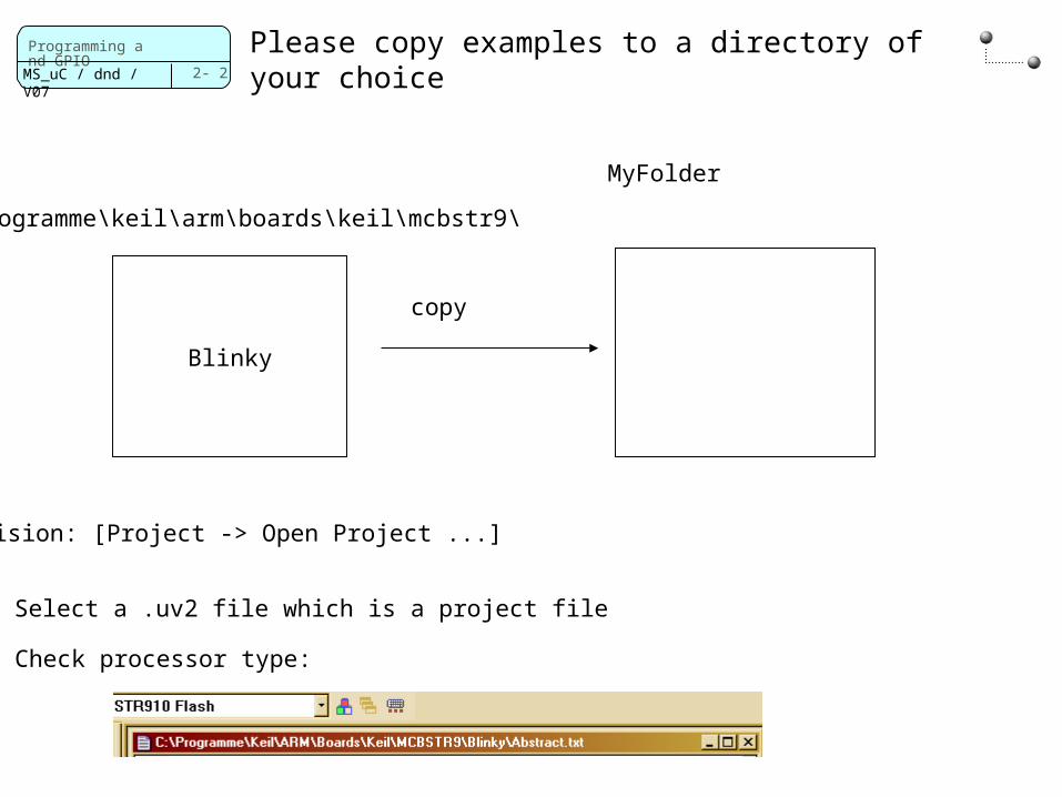
Please copy examples to a directory of your choice
Blinky
MyFolder
programme\keil\arm\boards\keil\mcbstr9\
copy
uVision: [Project -> Open Project ...]
Select a .uv2 file which is a project file
Check processor type:

2- 3
Programming and GPIO
MS_uC / dnd / V07
compiling Blinky.c...compiling LCD.c...compiling UserFont.c...linking...Program Size: Code=2264 RO-data=96 RW-data=4 ZI-data=1292 ".\Flash\Blinky.axf" - 0 Error(s), 0 Warning(s).
[Project -> Rebuild all target files]
No errors, no warnings is what
we like to see
Generated files are found in the Flash folder of the project directory:
2- 4
Programming and GPIO
MS_uC / dnd / V07
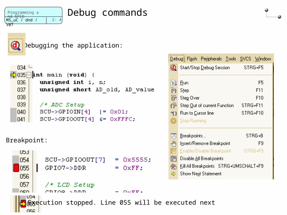
Debug commands
Debugging the application:
Breakpoint:
Execution stopped. Line 055 will be executed next

2- 5
Programming and GPIO
MS_uC / dnd / V07
Processor insight
Only accessible if target is not running

2- 6
Programming and GPIO
MS_uC / dnd / V07
System and Clock settings

2- 7
Programming and GPIO
MS_uC / dnd / V07
Peripheral Bridge 1 configuration"slow" peripherals
PCG1: Peripheral Clocking Gate Register 1: 0PRR1: Peripheral Reset Register 1: 0
GPIO7 enabled (LED)After Reset: ports disabled

2- 8
Programming and GPIO
MS_uC / dnd / V07
Definition
A GPIO is a digital binary signal Its switching level depends on the technology used A GPIO normally is programmable as unconnected,
input, output A GPIO might have built-in elements like pull-up,
pull-down or ESD devices A GP Output signal is able to sink (or source) a
defined amount of current A GP Input has a defined Impedance which might
be taken into account if a passive sensor is linked to it
A GP Input has a defined hysteresis to avoid "flippering" of the signal "Schmitt Trigger input"
2- 9
Programming and GPIO
MS_uC / dnd / V07
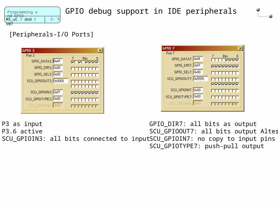
GPIO debug support in IDE peripherals
[Peripherals-I/O Ports]
P3 as inputP3.6 activeSCU_GPIOIN3: all bits connected to input
GPIO_DIR7: all bits as outputSCU_GPIOOUT7: all bits output Altern1SCU_GPIOIN7: no copy to input pinsSCU_GPIOTYPE7: push-pull output

2- 10
Programming and GPIO
MS_uC / dnd / V07
General Purpose I/O
Variable Pin attribution:

2- 11
Programming and GPIO
MS_uC / dnd / V07
Pin assignment for peripherals
Peripheral
# No of Unit
Port Assignment
IO Mode Peripheral
# No of Unit
Port Assignment
IO Mode
ADC 8 chann-els
P4 Always Connected
Motor Control
1 P6 Alt Out
CAN 1 P1, P3, P5 Alt In Alt out
SSP 2 P2, P5 Alt In Alt Out
ETM 1 P0,P2,P4,P5,P6, P7
Alt In Alt Out
Timers 4 P0, P4, P6, P7
Alt In Alt Out
Ethernet MAC
1 P0, P1, P5 Always Connected
UART 3 P1, P2, P3, P5, P6, P7
Alt In Alt Out
EMI Mux P8, P9, P7 P7 – Alt Out
USB 1 D+/D- Ext clk – P3
Dedicated pins
Non-mux
P8, P9, P7 P7 – Alt Out
External Interrupt
30 P3, P5, P6, P7
Always Connected
Chip Select
4 P0, P5, P7 Alt Out External DMA Req
2 P3 Always Connected
I2C 2 P0, P1, P2 Alt In Alt Out
2- 12
Programming and GPIO
MS_uC / dnd / V07
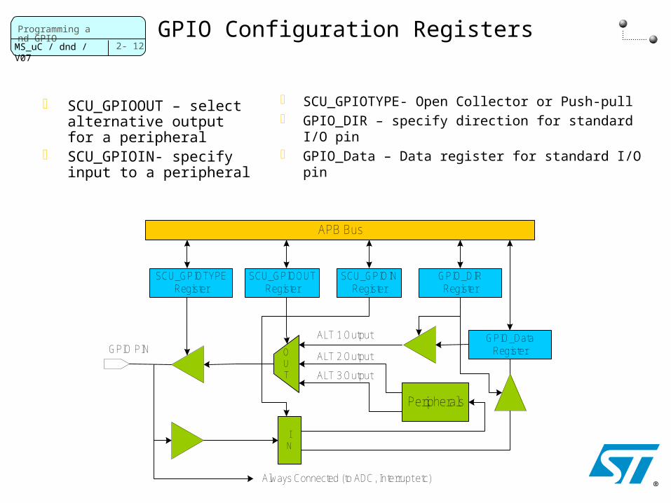
GPIO Configuration Registers
SCU_GPIOOUT – select alternative output for a peripheral
SCU_GPIOIN- specify input to a peripheral
SCU_GPIOTYPE- Open Collector or Push-pull GPIO_DIR – specify direction for standard I/O
pin GPIO_Data – Data register for standard I/O pin
SCU_GPIOTYPERegister
SCU_GPIOOUTRegister
GPIO_DIRRegister
GPIO_DataRegister
ALT 1 Output
Peripherals
ALT 2 Output
ALT 3 Output
APB Bus
SCU_GPIOINRegister
OUT
IN
Always Connected (to ADC, Interrupt etc)
GPIO PIN
®
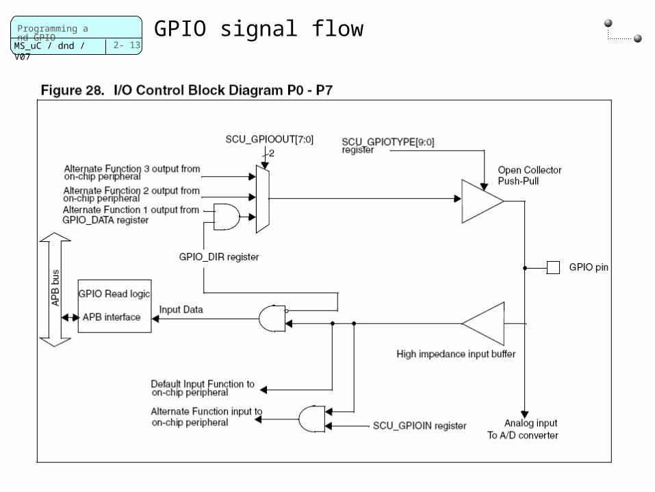
2- 13
Programming and GPIO
MS_uC / dnd / V07
GPIO signal flow

2- 14
Programming and GPIO
MS_uC / dnd / V07
GPIO registers
SCU_GPIOOUTn
SCU_GPIOINn
SCU_GPIOTYPEmPush-pullOpen collector
n : [9:2] Port number and alternate function
GPIO_DATA
GPIO_DIR
00h..3FCh [7..0]
GPIO_SEL
400h
420h
APB0_Base +
Ex: GPIO7 direction register non-buffered: 0x5800 D400
SCU_PCGR1_Val
SCU_PRR1_Val
In File STR91x.s:
Peripheral Clock Gating Register
Peripheral Reset Register

2- 15
Programming and GPIO
MS_uC / dnd / V07
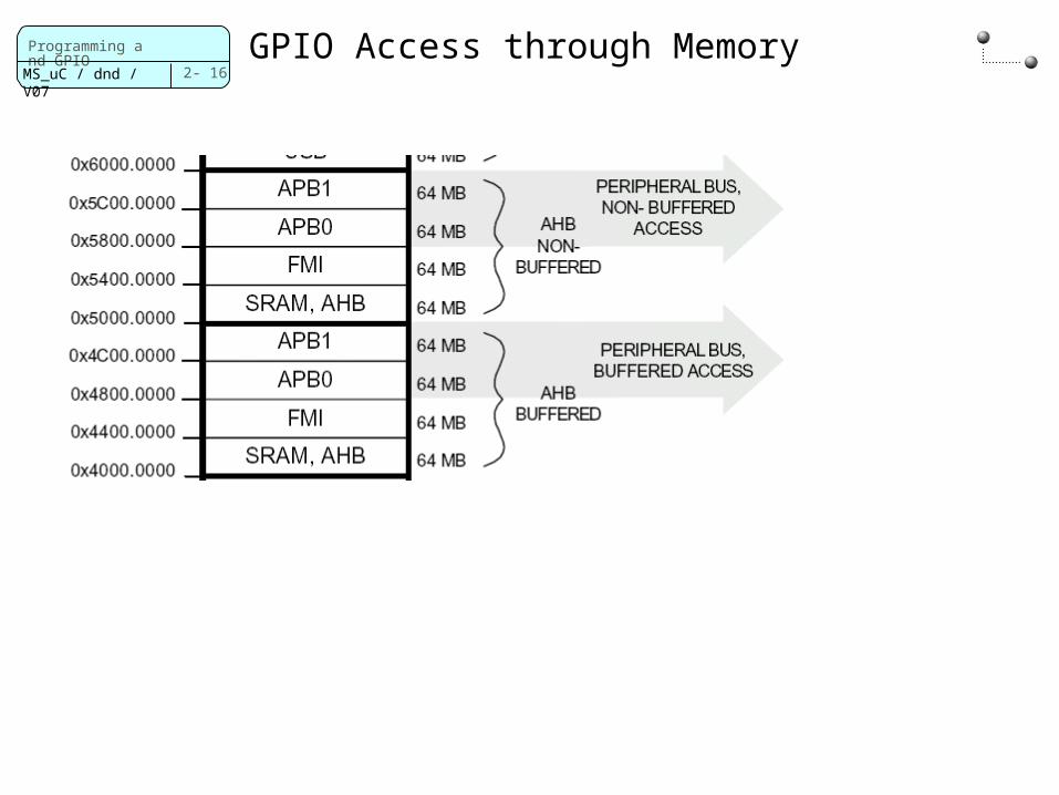
ARM Peripheral Bus 0 access (APB0)
2- 16
Programming and GPIO
MS_uC / dnd / V07
GPIO Access through Memory

2- 17
Programming and GPIO
MS_uC / dnd / V07
Library source
Library examples
2- 18
Programming and GPIO
MS_uC / dnd / V07
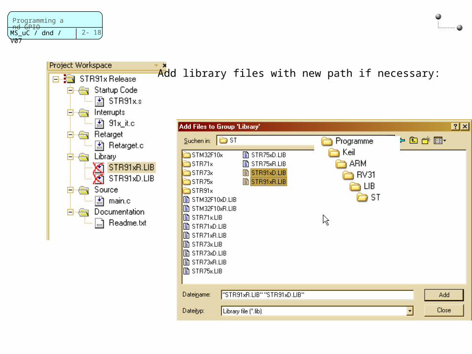
Add library files with new path if necessary:
2- 19
Programming and GPIO
MS_uC / dnd / V07
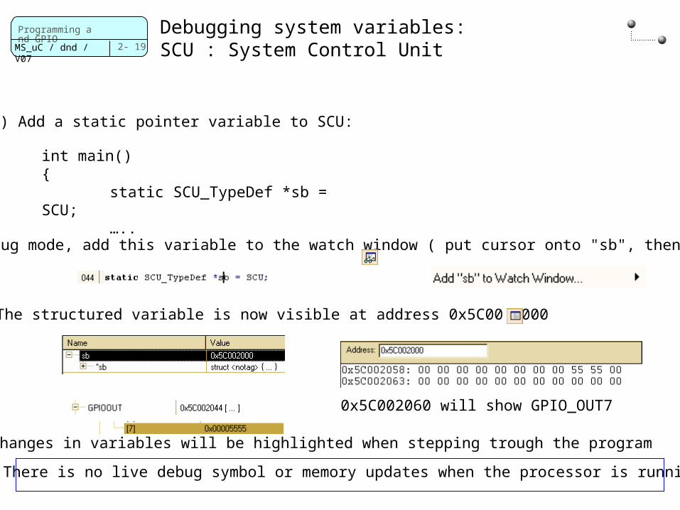
Debugging system variables: SCU : System Control Unit
1.) Add a static pointer variable to SCU:
int main(){
static SCU_TypeDef *sb = SCU;…..
2.) In Debug mode, add this variable to the watch window ( put cursor onto "sb", then right click)
3.) The structured variable is now visible at address 0x5C00 2000
Changes in variables will be highlighted when stepping trough the program
There is no live debug symbol or memory updates when the processor is running
0x5C002060 will show GPIO_OUT7