MSE-630 Gallium Arsenide Semiconductors. MSE-630 Overview Compound Semiconductor Materials Interest...
23
MSE-630 Gallium Arsenide Semiconductors
-
Upload
christal-hamilton -
Category
Documents
-
view
231 -
download
2
Transcript of MSE-630 Gallium Arsenide Semiconductors. MSE-630 Overview Compound Semiconductor Materials Interest...

MSE-630
Gallium Arsenide Semiconductors

MSE-630
Overview
•Compound Semiconductor Materials
•Interest in GaAs
•Physical Properties
•Processing Methods
•Applications
MSE-630
MSE-630
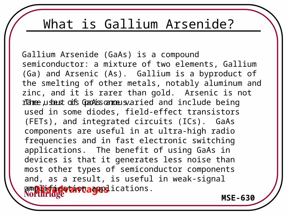
What is Gallium Arsenide?
Gallium Arsenide (GaAs) is a compound semiconductor: a mixture of two elements, Gallium (Ga) and Arsenic (As). Gallium is a byproduct of the smelting of other metals, notably aluminum and zinc, and it is rarer than gold. Arsenic is not rare, but is poisonous.
Disadvantages
The uses of GaAs are varied and include being used in some diodes, field-effect transistors (FETs), and integrated circuits (ICs). GaAs components are useful in at ultra-high radio frequencies and in fast electronic switching applications. The benefit of using GaAs in devices is that it generates less noise than most other types of semiconductor components and, as a result, is useful in weak-signal amplification applications.

MSE-630
Advantages and Disadvantages of GaAS
•Very high electron mobility
•High thermal stability
•Low noise
•Wide temperature operating range
Advantages Disadvantages•No natural oxide as in Silicon
•High production costs
•Small size (4”) ingots
Unlike silicon cells, Gallium Arsenide cells are relatively insensitive to heat. Alloys made from GaAs using Al, P, SB, or In have characteristics complementary to those of GaAs, allowing great flexibility.
GaAs is very resistant to radiation damage. This, along with its high efficiency, makes GaAs very desirable for space applications. However, GaAs does nave drawbacks; the greatest barrier is the high cost of a single-crystal GaAs substrate.

MSE-630
GaAs and Other Compound Semiconducors

MSE-630
MSE-630

Crystal Structure
MSE-630
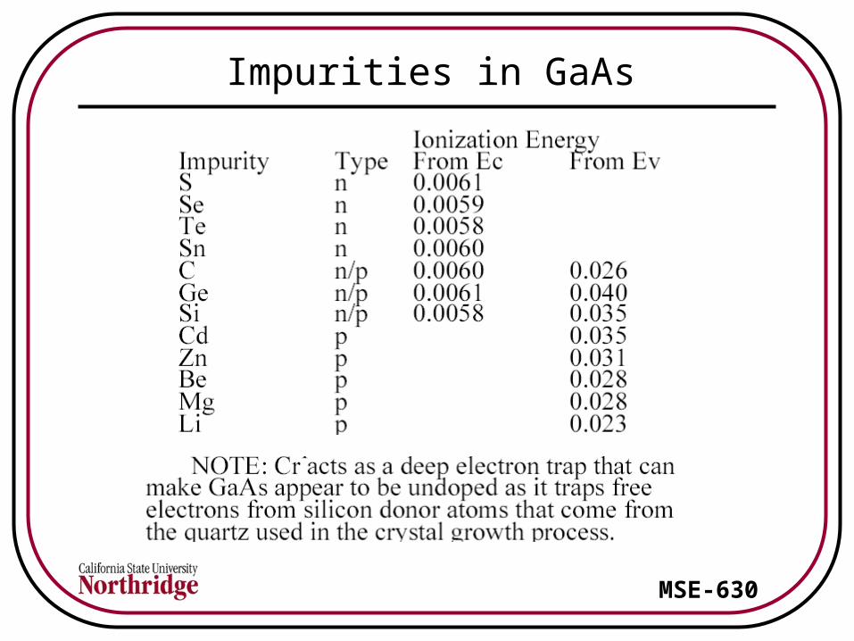
Impurities in GaAs
MSE-630

Energy Band Structure
Direct gap semiconductor
Energy gap = 1.43 eV
Indirect gap semiconductor
Energy gap = 1.12 eV
MSE-630

Hole Concentration
Electron Mobility at 77K and 300K
Electron and Hole Mobility
Hole Mobility at 77K and 300K
MSE-630

MSE-630
Electron Drift Velocity
Note that drift velocity slows in fields exceeding ~ 1000 V/cm

MSE-630
GaAs does not grow a native oxide that is equivalent to SiO2. Ga2O3 and As2O3 and As2O5 oxides that grow on GaAs present more problems than uses
The vapor pressure of As in GaAs is very low. A GaAs substrate hated to about 500 C begins to lose As from the surface. The wafer can be capped with SiO2 or Si3N4 or the heat treating can be carried out in an Arsenic overpressure. GaAs crystals are often grown in the horizongal Bridgeman technique and the wafers are “D” shaped. Czochralski GaAS wafers are also available up to ~4” in diameter. GaAs wafes are more brittle than Si wafers. 4” GaAs wafers cost about $300 each.
MSE-630
MSE-630
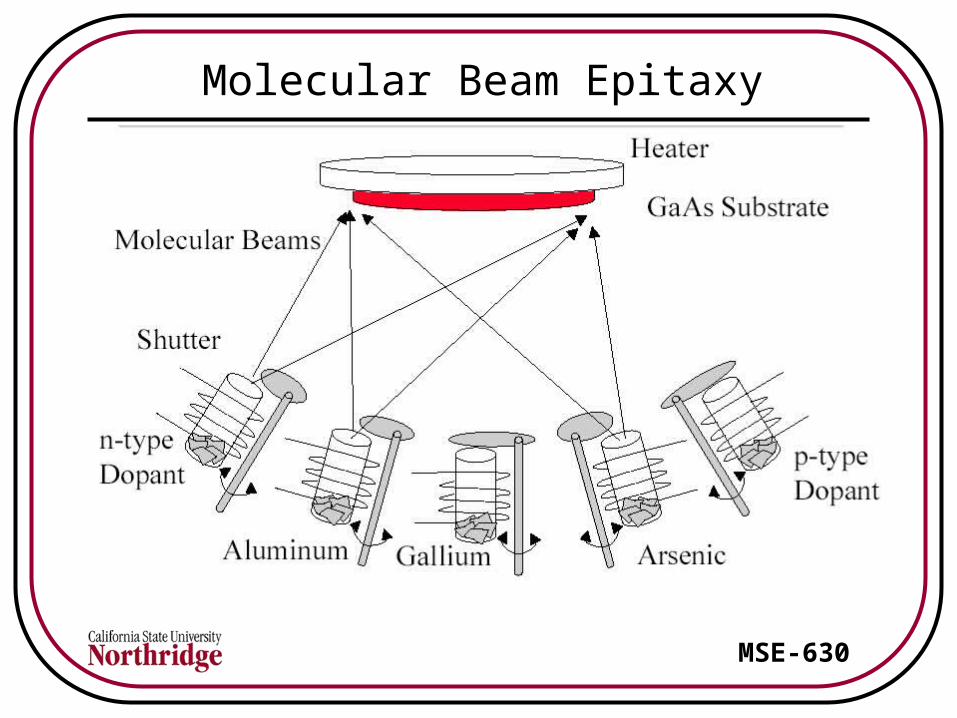
Molecular Beam Epitaxy
MSE-630
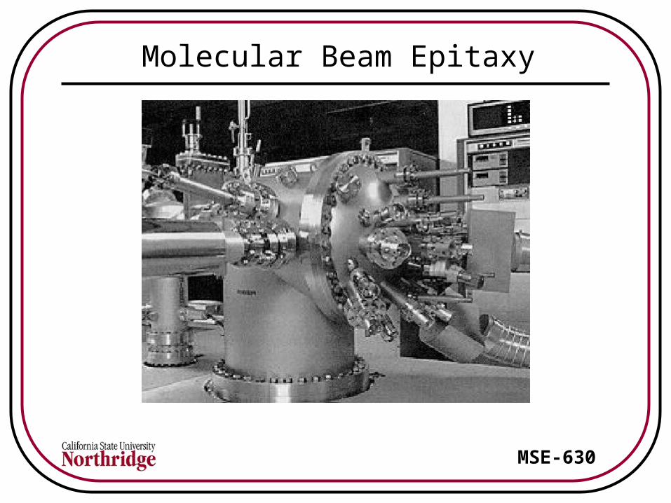
Molecular Beam Epitaxy
MSE-630
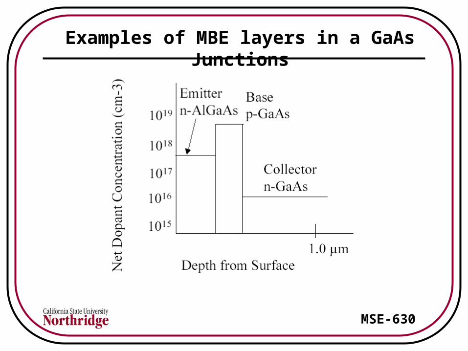
Examples of MBE layers in a GaAs Junctions
MSE-630
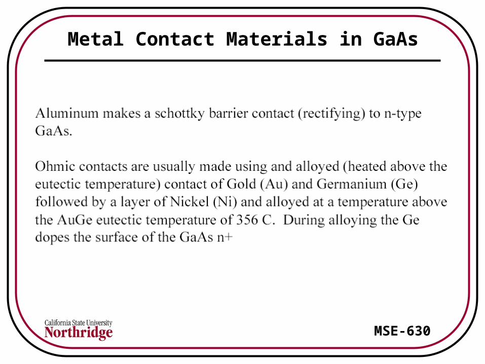
Metal Contact Materials in GaAs

MSE-630
MSE-630

MSE-630
GaAs Processing
Starting wafer
First Photoresist for Channel Stop
Alignment & Channel Stop
Implant
First Encapsulation
2nd Photo Channel Etch
2nd Photo Channel Etch
MSE-630
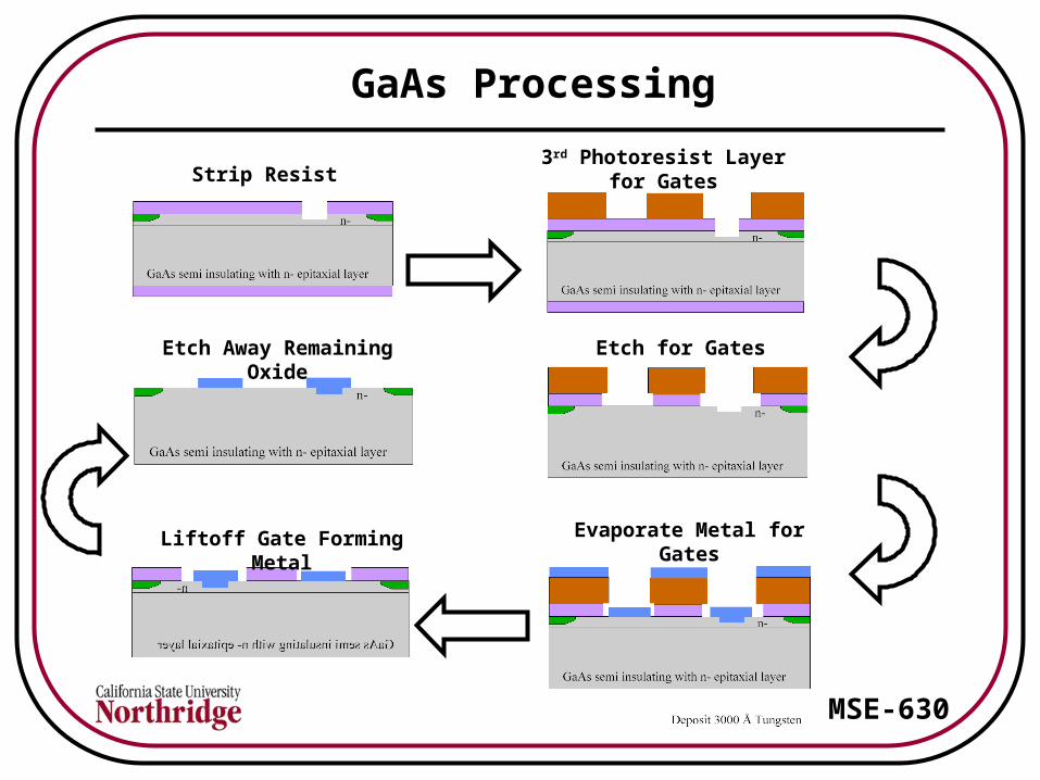
GaAs Processing
Strip Resist3rd Photoresist Layer for
Gates
Etch for Gates
Evaporate Metal for GatesLiftoff Gate Forming Metal
Etch Away Remaining Oxide
MSE-630
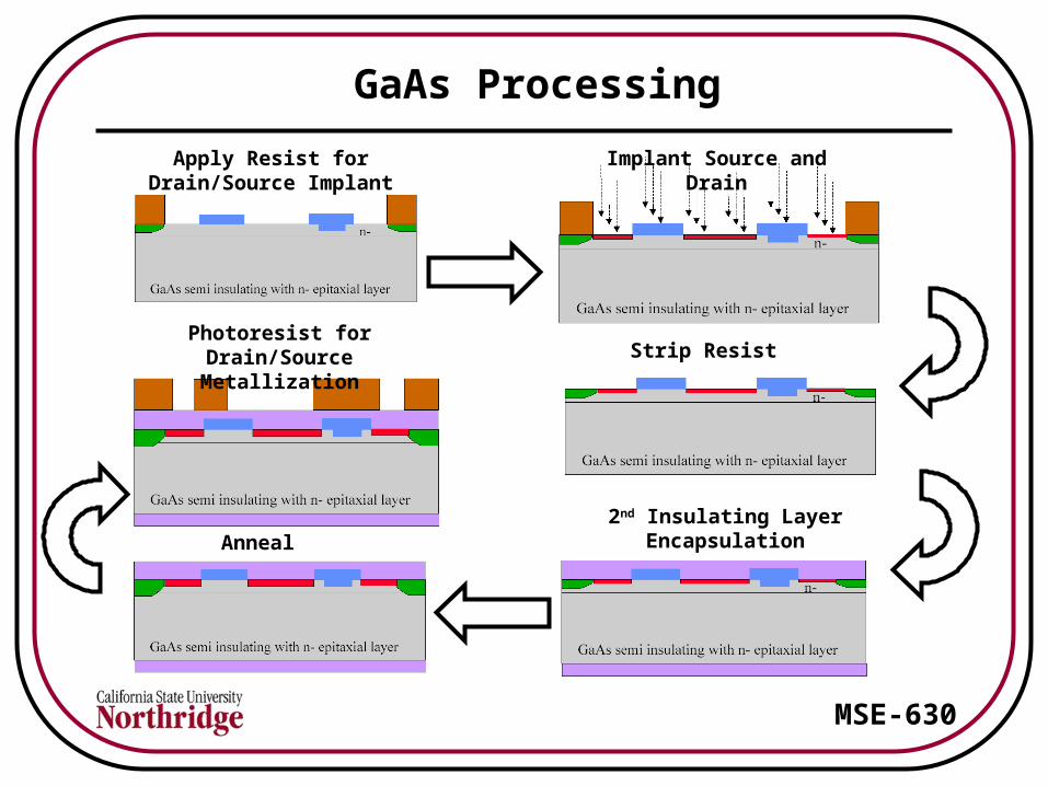
GaAs Processing
Apply Resist for Drain/Source Implant
Strip Resist
Implant Source and Drain
2nd Insulating Layer EncapsulationAnneal
Photoresist for Drain/Source Metallization

MSE-630
GaAs Processing
Etch Oxide Evaporate Source/Drain Metal
Liftoff Resist
Add Connectors

MSE-630
Summary
MSE-630
The
End