MPU-9150 Register Map and Descriptions Revision 4 · The MPU-9150Motion Processing Unit is the...
60
InvenSense Inc. 1197 Borregas Ave, Sunnyvale, CA 94089 U.S.A. Tel: +1 (408) 988-7339 Fax: +1 (408) 988-8104 Website: www.invensense.com Document Number: RM-MPU-9150A-00 Revision: 4.0 Release Date: 09/12/2012 1 of 60 MPU-9150 Register Map and Descriptions Revision 4.0
Transcript of MPU-9150 Register Map and Descriptions Revision 4 · The MPU-9150Motion Processing Unit is the...
InvenSense Inc. 1197 Borregas Ave, Sunnyvale, CA 94089 U.S.A. Tel: +1 (408) 988-7339 Fax: +1 (408) 988-8104
Website: www.invensense.com
Document Number: RM-MPU-9150A-00 Revision: 4.0 Release Date: 09/12/2012
1 of 60
MPU-9150 Register Map and Descriptions
Revision 4.0

MPU-9150 Register Map and Descriptions
Document Number: RM-MPU-9150A-00 Revision: 4.0 Release Date: 09/12/2012
2 of 60
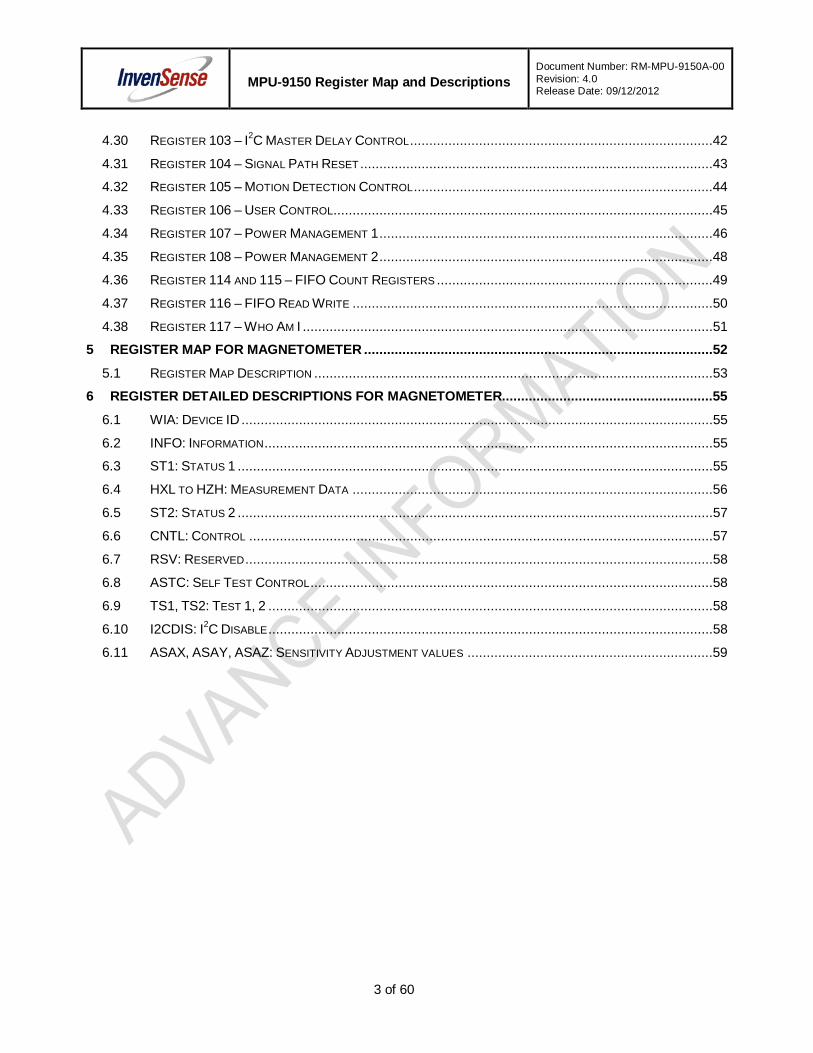
CONTENTS 1 REVISION HISTORY ............................................................................................................................. 4
2 PURPOSE AND SCOPE ....................................................................................................................... 5
3 REGISTER MAP FOR GYROSCOPE AND ACCELEROMETER ........................................................... 6
4 REGISTER DESCRIPTIONS FOR GYROSCOPE AND ACCELEROMETER ........................................ 9
4.1 REGISTERS 13 TO 16 – SELF TEST REGISTERS ................................................................................ 9
4.2 REGISTER 25 – SAMPLE RATE DIVIDER ...........................................................................................11
4.3 REGISTER 26 – CONFIGURATION ....................................................................................................13
4.4 REGISTER 27 – GYROSCOPE CONFIGURATION.................................................................................14
4.5 REGISTER 28 – ACCELEROMETER CONFIGURATION..........................................................................15
4.6 REGISTER 31 – MOTION DETECTION THRESHOLD ............................................................................17
4.7 REGISTER 32 – MOTION DETECTION DURATION ...............................................................................17
4.8 REGISTER 33 – ZERO MOTION DETECTION THRESHOLD ...................................................................19
4.9 REGISTER 34 – ZERO MOTION DETECTION DURATION ......................................................................19
4.10 REGISTER 35 – FIFO ENABLE .......................................................................................................20
4.11 REGISTER 36 – I2C MASTER CONTROL ...........................................................................................21
4.12 REGISTERS 37 TO 39 – I2C SLAVE 0 CONTROL ................................................................................23
4.13 REGISTERS 40 TO 42 – I2C SLAVE 1 CONTROL ................................................................................26
4.14 REGISTERS 43 TO 45 – I2C SLAVE 2 CONTROL ................................................................................26
4.15 REGISTERS 46 TO 48 – I2C SLAVE 3 CONTROL ................................................................................26
4.16 REGISTERS 49 TO 53 – I2C SLAVE 4 CONTROL ................................................................................27
4.17 REGISTER 54 – I2C MASTER STATUS ..............................................................................................29
4.18 REGISTER 55 – INT PIN / BYPASS ENABLE CONFIGURATION .............................................................30
4.19 REGISTER 56 – INTERRUPT ENABLE ...............................................................................................32
4.20 REGISTER 58 – INTERRUPT STATUS ...............................................................................................33
4.21 REGISTERS 59 TO 64 – ACCELEROMETER MEASUREMENTS ..............................................................34
4.22 REGISTERS 65 AND 66 – TEMPERATURE MEASUREMENT ..................................................................35
4.23 REGISTERS 67 TO 72 – GYROSCOPE MEASUREMENTS .....................................................................36
4.24 REGISTERS 73 TO 96 – EXTERNAL SENSOR DATA ............................................................................37
4.25 REGISTER 97 – MOTION DETECTION STATUS ..................................................................................39
4.26 REGISTER 99 – I2C SLAVE 0 DATA OUT ..........................................................................................40
4.27 REGISTER 100 – I2C SLAVE 1 DATA OUT ........................................................................................40
4.28 REGISTER 101 – I2C SLAVE 2 DATA OUT ........................................................................................41
4.29 REGISTER 102 – I2C SLAVE 3 DATA OUT ........................................................................................41
MPU-9150 Register Map and Descriptions
Document Number: RM-MPU-9150A-00 Revision: 4.0 Release Date: 09/12/2012
3 of 60
4.30 REGISTER 103 – I2C MASTER DELAY CONTROL ...............................................................................42
4.31 REGISTER 104 – SIGNAL PATH RESET ............................................................................................43
4.32 REGISTER 105 – MOTION DETECTION CONTROL ..............................................................................44
4.33 REGISTER 106 – USER CONTROL...................................................................................................45
4.34 REGISTER 107 – POWER MANAGEMENT 1 .......................................................................................46
4.35 REGISTER 108 – POWER MANAGEMENT 2 .......................................................................................48
4.36 REGISTER 114 AND 115 – FIFO COUNT REGISTERS ........................................................................49
4.37 REGISTER 116 – FIFO READ WRITE ..............................................................................................50
4.38 REGISTER 117 – WHO AM I ...........................................................................................................51
5 REGISTER MAP FOR MAGNETOMETER ...........................................................................................52
5.1 REGISTER MAP DESCRIPTION ........................................................................................................53
6 REGISTER DETAILED DESCRIPTIONS FOR MAGNETOMETER.......................................................55
6.1 WIA: DEVICE ID ...........................................................................................................................55
6.2 INFO: INFORMATION .....................................................................................................................55
6.3 ST1: STATUS 1 ............................................................................................................................55
6.4 HXL TO HZH: MEASUREMENT DATA ..............................................................................................56
6.5 ST2: STATUS 2 ............................................................................................................................57
6.6 CNTL: CONTROL .........................................................................................................................57
6.7 RSV: RESERVED ..........................................................................................................................58
6.8 ASTC: SELF TEST CONTROL .........................................................................................................58
6.9 TS1, TS2: TEST 1, 2 ....................................................................................................................58
6.10 I2CDIS: I2C DISABLE ....................................................................................................................58
6.11 ASAX, ASAY, ASAZ: SENSITIVITY ADJUSTMENT VALUES ................................................................59
MPU-9150 Register Map and Descriptions
Document Number: RM-MPU-9150A-00 Revision: 4.0 Release Date: 09/12/2012
4 of 60
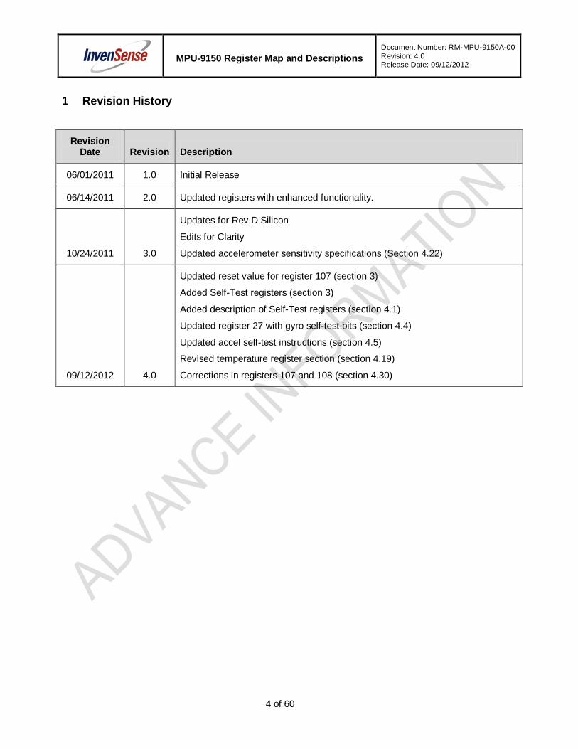
1 Revision History
Revision Date Revision Description
06/01/2011 1.0 Initial Release
06/14/2011 2.0 Updated registers with enhanced functionality.
10/24/2011 3.0
Updates for Rev D Silicon
Edits for Clarity
Updated accelerometer sensitivity specifications (Section 4.22)
09/12/2012 4.0
Updated reset value for register 107 (section 3) Added Self-Test registers (section 3) Added description of Self-Test registers (section 4.1) Updated register 27 with gyro self-test bits (section 4.4) Updated accel self-test instructions (section 4.5)
Revised temperature register section (section 4.19) Corrections in registers 107 and 108 (section 4.30)

MPU-9150 Register Map and Descriptions
Document Number: RM-MPU-9150A-00 Revision: 4.0 Release Date: 09/12/2012
5 of 60
2 Purpose and Scope This document provides preliminary information regarding the register map and descriptions for the MPU-9150™ Motion Processing Unit™ or MPU™.
The MPU-9150 Motion Processing Unit is the world’s first motion processing solution with integrated 9-Axis sensor fusion using its field-proven and proprietary MotionFusion™ engine for handset and tablet applications, game controllers, motion pointer remote controls, and other consumer devices. The MPU-9150 has an embedded 3-axis MEMS gyroscope, a 3-axis MEMS accelerometer, a 3-axis MEMS magnetometer and a Digital Motion Processor™ (DMP™) hardware accelerator engine with an auxiliary I2C port that interfaces to 3rd party digital sensors such as pressure sensors. The MPU-9150’s 9-axis MotionFusion combines acceleration and rotational motion plus heading information into a single data stream for the application. This MotionProcessing™ technology integration provides a smaller footprint and has inherent cost advantages compared to discrete gyroscope, accelerometer, plus magnetometer solutions. The MPU-9150 is also designed to interface with multiple non-inertial digital sensors, such as pressure sensors, on its auxiliary I2C port to produce a 10-Axis sensor fusion output. The MPU-9150 is a 3rd generation motion processor and is footprint compatible with the MPU-60X0 and MPU-30X0 families.
The MPU-9150 features three 16-bit analog-to-digital converters (ADCs) for digitizing the gyroscope outputs, three 16-bit ADCs for digitizing the accelerometer outputs, and three 13-bit ADCs for digitizing the magnetometer outputs. For precision tracking of both fast and slow motions, the parts feature a user-programmable gyroscope full-scale range of ±250, ±500, ±1000, and ±2000°/sec (dps), a user-programmable accelerometer full-scale range of ±2g, ±4g, ±8g, and ±16g, and a magnetometer full-scale range of ±1200µT.
The MPU-9150 is a multi-chip module (MCM) consisting of two dies integrated into a single LGA package. One die houses the 3-Axis gyroscope and the 3-Axis accelerometer. The other die houses the AK9875C 3-Axis magnetometer from Asahi Kasei Microdevices Corporation.
An on-chip 1024 Byte FIFO buffer helps lower system power consumption by allowing the system processor to read the sensor data in bursts and then enter a low-power mode as the MPU collects more data. With all the necessary on-chip processing and sensor components required to support many motion-based use cases, the MPU-9150 uniquely supports a variety of advanced motion-based applications entirely on-chip. The MPU-9150 thus enables low-power MotionProcessing in portable applications with reduced processing requirements for the system processor. By providing an integrated MotionFusion output, the DMP in the MPU-9150 offloads the intensive MotionProcessing computation requirements from the system processor, minimizing the need for frequent polling of the motion sensor output.
Communication with all registers of the device is performed using I2C at 400kHz. Additional features include an embedded temperature sensor and an on-chip oscillator with ±1% variation over the operating temperature range.
For more detailed information for the MPU-9150 device, please refer to the MPU-9150 Product Specification document.

MPU-9150 Register Map and Descriptions
Document Number: RM-MPU-9150A-00 Revision: 4.0 Release Date: 09/12/2012
6 of 60
3 Register Map for Gyroscope and Accelerometer The register map for the MPU-9150’s Gyroscope and Accelerometer section is listed below. The Magnetometer’s register map can be found in section 5.
Addr (Hex)
Addr (Dec.) Register Name Serial
I/F Bit7 Bit6 Bit5 Bit4 Bit3 Bit2 Bit1 Bit0
0D 13 SELF_TEST_X R/W XA_TEST[4-2] XG_TEST[4-0]
0E 14 SELF_TEST_Y R/W YA_TEST[4-2] YG_TEST[4-0]
0F 15 SELF_TEST_Z R/W ZA_TEST[4-2] ZG_TEST[4-0]
10 16 SELF_TEST_A R/W RESERVED XA_TEST[1-0] YA_TEST[1-0] ZA_TEST[1-0]
19 25 SMPLRT_DIV R/W SMPLRT_DIV[7:0]
1A 26 CONFIG R/W - - EXT_SYNC_SET[2:0] DLPF_CFG[2:0]
1B 27 GYRO_CONFIG R/W XG_ST YG_ST ZG_ST FS_SEL [1:0] - - -
1C 28 ACCEL_CONFIG R/W XA_ST YA_ST ZA_ST AFS_SEL[1:0] ACCEL_HPF[2:0]
1D 29 FF_THR R/W FF_THR[7:0]
1E 30 FF_DUR R/W FF_DUR[7:0]
1F 31 MOT_THR R/W MOT_THR[7:0]
20 32 MOT_DUR R/W MOT_DUR[7:0]
21 33 ZRMOT_THR R/W ZRMOT_THR[7:0]
22 34 ZRMOT_DUR R/W ZRMOT_DUR[7:0]
23 35 FIFO_EN R/W TEMP _FIFO_EN
XG _FIFO_EN
YG _FIFO_EN
ZG _FIFO_EN
ACCEL _FIFO_EN
SLV2 _FIFO_EN
SLV1 _FIFO_EN
SLV0 _FIFO_EN
24 36 I2C_MST_CTRL R/W MULT _MST_EN
WAIT _FOR_ES
SLV_3 _FIFO_EN
I2C_MST _P_NSR I2C_MST_CLK[3:0]
25 37 I2C_SLV0_ADDR R/W I2C_SLV0 _RW I2C_SLV0_ADDR[6:0]
26 38 I2C_SLV0_REG R/W I2C_SLV0_REG[7:0]
27 39 I2C_SLV0_CTRL R/W I2C_SLV0 _EN
I2C_SLV0 _BYTE_SW
I2C_SLV0 _REG_DIS
I2C_SLV0 _GRP I2C_SLV0_LEN[3:0]
28 40 I2C_SLV1_ADDR R/W I2C_SLV1 _RW I2C_SLV1_ADDR[6:0]
29 41 I2C_SLV1_REG R/W I2C_SLV1_REG[7:0]
2A 42 I2C_SLV1_CTRL R/W I2C_SLV1 _EN
I2C_SLV1 _BYTE_SW
I2C_SLV1 _REG_DIS
I2C_SLV1 _GRP I2C_SLV1_LEN[3:0]
2B 43 I2C_SLV2_ADDR R/W I2C_SLV2 _RW I2C_SLV2_ADDR[6:0]
2C 44 I2C_SLV2_REG R/W I2C_SLV2_REG[7:0]
2D 45 I2C_SLV2_CTRL R/W I2C_SLV2 _EN
I2C_SLV2 _BYTE_SW
I2C_SLV2 _REG_DIS
I2C_SLV2 _GRP I2C_SLV2_LEN[3:0]
2E 46 I2C_SLV3_ADDR R/W I2C_SLV3 _RW I2C_SLV3_ADDR[6:0]
2F 47 I2C_SLV3_REG R/W I2C_SLV3_REG[7:0]
30 48 I2C_SLV3_CTRL R/W I2C_SLV3 _EN
I2C_SLV3 _BYTE_SW
I2C_SLV3 _REG_DIS
I2C_SLV3 _GRP I2C_SLV3_LEN[3:0]
31 49 I2C_SLV4_ADDR R/W I2C_SLV4 _RW I2C_SLV4_ADDR[6:0]
32 50 I2C_SLV4_REG R/W I2C_SLV4_REG[7:0]
33 51 I2C_SLV4_DO R/W I2C_SLV4_DO[7:0]
34 52 I2C_SLV4_CTRL R/W I2C_SLV4 _EN
I2C_SLV4 _INT_EN
I2C_SLV4 _REG_DIS I2C_MST_DLY[4:0]
35 53 I2C_SLV4_DI R I2C_SLV4_DI[7:0]

MPU-9150 Register Map and Descriptions
Document Number: RM-MPU-9150A-00 Revision: 4.0 Release Date: 09/12/2012
7 of 60
Addr (Hex)
Addr (Dec.) Register Name Serial
I/F Bit7 Bit6 Bit5 Bit4 Bit3 Bit2 Bit1 Bit0
36 54 I2C_MST_STATUS R PASS_ THROUGH
I2C_SLV4 _DONE
I2C_LOST _ARB
I2C_SLV4 _NACK
I2C_SLV3 _NACK
I2C_SLV2 _NACK
I2C_SLV1 _NACK
I2C_SLV0 _NACK
37 55 INT_PIN_CFG R/W INT_LEVEL INT_OPEN LATCH _INT_EN
INT_RD _CLEAR
FSYNC_ INT_LEVEL
FSYNC _INT_EN
I2C _BYPASS
_EN
CLKOUT _EN
38 56 INT_ENABLE R/W FF_EN MOT_EN ZMOT_EN FIFO
_OFLOW _EN
I2C_MST _INT_EN - - DATA
_RDY_EN
3A 58 INT_STATUS R FF_INT MOT_INT ZMOT _INT
FIFO _OFLOW
_INT
I2C_MST _INT - - DATA
_RDY_INT
3B 59 ACCEL_XOUT_H R ACCEL_XOUT[15:8]
3C 60 ACCEL_XOUT_L R ACCEL_XOUT[7:0]
3D 61 ACCEL_YOUT_H R ACCEL_YOUT[15:8]
3E 62 ACCEL_YOUT_L R ACCEL_YOUT[7:0]
3F 63 ACCEL_ZOUT_H R ACCEL_ZOUT[15:8]
40 64 ACCEL_ZOUT_L R ACCEL_ZOUT[7:0]
41 65 TEMP_OUT_H R TEMP_OUT[15:8]
42 66 TEMP_OUT_L R TEMP_OUT[7:0]
43 67 GYRO_XOUT_H R GYRO_XOUT[15:8]
44 68 GYRO_XOUT_L R GYRO_XOUT[7:0]
45 69 GYRO_YOUT_H R GYRO_YOUT[15:8]
46 70 GYRO_YOUT_L R GYRO_YOUT[7:0]
47 71 GYRO_ZOUT_H R GYRO_ZOUT[15:8]
48 72 GYRO_ZOUT_L R GYRO_ZOUT[7:0]
49 73 EXT_SENS_DATA_00 R EXT_SENS_DATA_00[7:0]
4A 74 EXT_SENS_DATA_01 R EXT_SENS_DATA_01[7:0]
4B 75 EXT_SENS_DATA_02 R EXT_SENS_DATA_02[7:0]
4C 76 EXT_SENS_DATA_03 R EXT_SENS_DATA_03[7:0]
4D 77 EXT_SENS_DATA_04 R EXT_SENS_DATA_04[7:0]
4E 78 EXT_SENS_DATA_05 R EXT_SENS_DATA_05[7:0]
4F 79 EXT_SENS_DATA_06 R EXT_SENS_DATA_06[7:0]
50 80 EXT_SENS_DATA_07 R EXT_SENS_DATA_07[7:0]
51 81 EXT_SENS_DATA_08 R EXT_SENS_DATA_08[7:0]
52 82 EXT_SENS_DATA_09 R EXT_SENS_DATA_09[7:0]
53 83 EXT_SENS_DATA_10 R EXT_SENS_DATA_10[7:0]
54 84 EXT_SENS_DATA_11 R EXT_SENS_DATA_11[7:0]
55 85 EXT_SENS_DATA_12 R EXT_SENS_DATA_12[7:0]
56 86 EXT_SENS_DATA_13 R EXT_SENS_DATA_13[7:0]
57 87 EXT_SENS_DATA_14 R EXT_SENS_DATA_14[7:0]
58 88 EXT_SENS_DATA_15 R EXT_SENS_DATA_15[7:0]
59 89 EXT_SENS_DATA_16 R EXT_SENS_DATA_16[7:0]
5A 90 EXT_SENS_DATA_17 R EXT_SENS_DATA_17[7:0]
5B 91 EXT_SENS_DATA_18 R EXT_SENS_DATA_18[7:0]
5C 92 EXT_SENS_DATA_19 R EXT_SENS_DATA_19[7:0]
MPU-9150 Register Map and Descriptions
Document Number: RM-MPU-9150A-00 Revision: 4.0 Release Date: 09/12/2012
8 of 60
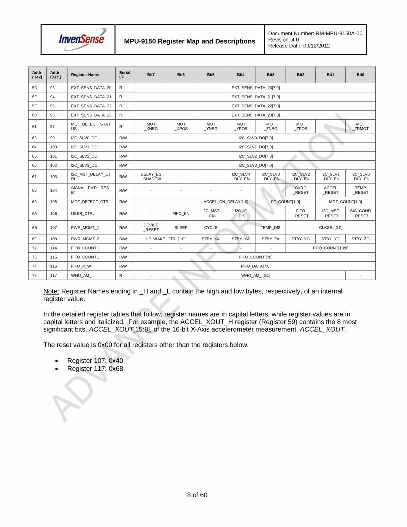
Addr (Hex)
Addr (Dec.) Register Name Serial
I/F Bit7 Bit6 Bit5 Bit4 Bit3 Bit2 Bit1 Bit0
5D 93 EXT_SENS_DATA_20 R EXT_SENS_DATA_20[7:0]
5E 94 EXT_SENS_DATA_21 R EXT_SENS_DATA_21[7:0]
5F 95 EXT_SENS_DATA_22 R EXT_SENS_DATA_22[7:0]
60 96 EXT_SENS_DATA_23 R EXT_SENS_DATA_23[7:0]
61 97 MOT_DETECT_STATUS R MOT
_XNEG MOT
_XPOS MOT
_YNEG MOT
_YPOS MOT
_ZNEG MOT
_ZPOS - MOT _ZRMOT
63 99 I2C_SLV0_DO R/W I2C_SLV0_DO[7:0]
64 100 I2C_SLV1_DO R/W I2C_SLV1_DO[7:0]
65 101 I2C_SLV2_DO R/W I2C_SLV2_DO[7:0]
66 102 I2C_SLV3_DO R/W I2C_SLV3_DO[7:0]
67 103 I2C_MST_DELAY_CTRL R/W DELAY_ES
_SHADOW - - I2C_SLV4 _DLY_EN
I2C_SLV3 _DLY_EN
I2C_SLV2 _DLY_EN
I2C_SLV1 _DLY_EN
I2C_SLV0 _DLY_EN
68 104 SIGNAL_PATH_RESET R/W - - - - - GYRO
_RESET ACCEL
_RESET TEMP
_RESET
69 105 MOT_DETECT_CTRL R/W - - ACCEL_ON_DELAY[1:0] FF_COUNT[1:0] MOT_COUNT[1:0]
6A 106 USER_CTRL R/W - FIFO_EN I2C_MST
_EN I2C_IF _DIS -
FIFO _RESET
I2C_MST _RESET
SIG_COND _RESET
6B 107 PWR_MGMT_1 R/W DEVICE _RESET SLEEP CYCLE - TEMP_DIS CLKSEL[2:0]
6C 108 PWR_MGMT_2 R/W LP_WAKE_CTRL[1:0] STBY_XA STBY_YA STBY_ZA STBY_XG STBY_YG STBY_ZG
72 114 FIFO_COUNTH R/W - - - - - FIFO_COUNT[10:8]
73 115 FIFO_COUNTL R/W FIFO_COUNT[7:0]
74 116 FIFO_R_W R/W FIFO_DATA[7:0]
75 117 WHO_AM_I R - WHO_AM_I[6:1] -
Note:
Register Names ending in _H and _L contain the high and low bytes, respectively, of an internal register value.
In the detailed register tables that follow, register names are in capital letters, while register values are in capital letters and italicized. For example, the ACCEL_XOUT_H register (Register 59) contains the 8 most significant bits, ACCEL_XOUT[15:8], of the 16-bit X-Axis accelerometer measurement, ACCEL_XOUT. The reset value is 0x00 for all registers other than the registers below.
• Register 107: 0x40. • Register 117: 0x68.

MPU-9150 Register Map and Descriptions
Document Number: RM-MPU-9150A-00 Revision: 4.0 Release Date: 09/12/2012
9 of 60
4 Register Descriptions for Gyroscope and Accelerometer This section details each register within the MPU-9150’s Gyroscope and Accelerometer sections.
Note:
The device will come up in sleep mode upon power up.
4.1 Registers 13 to 16 – Self Test Registers SELF_TEST_X, SELF_TEST_Y, SELF_TEST_Z, and SELF_TEST_A
Type: Read/Write Register
(Hex) Register (Decimal) Bit7 Bit6 Bit5 Bit4 Bit3 Bit2 Bit1 Bit0
0D 13 XA_TEST[4-2] XG_TEST[4-0] 0E 14 YA_TEST[4-2] YG_TEST[4-0] 0F 15 ZA_TEST[4-2] ZG_TEST[4-0] 10 16 RESERVED XA_TEST[1-0] YA_TEST[1-0] ZA_TEST[1-0]
These registers are used to hold the Factory trim values of the self-test response for the gyroscope.
Description:
Following is a description of the relative self-test method for the gyroscope and accelerometer.
Gyroscope Hardware Self-Test: Relative Method Gyroscope self-test permits users to test the mechanical and electrical portions of the gyroscope via the procedure in Obtaining the Gyroscope Factory Trim (FT) Value below.
When self-test is activated, the on-board electronics will actuate the appropriate sensor. Please refer to the register 27 for the corresponding bits to activate the self-test. This actuation will move the sensor’s proof masses over a distance equivalent to a pre-defined Coriolis force. This proof mass displacement results in a change in the sensor output, which is reflected in the output signal. The output signal is used to observe the self-test response.
The self-test response (STR) is defined as follows:
𝑆𝑒𝑙𝑓𝑇𝑒𝑠𝑡 𝑅𝑒𝑠𝑝𝑜𝑛𝑠𝑒 =
𝐺𝑦𝑟𝑜𝑠𝑐𝑜𝑝𝑒 𝑂𝑢𝑡𝑝𝑢𝑡 𝑤𝑖𝑡ℎ 𝑆𝑒𝑙𝑓-𝑇𝑒𝑠𝑡 𝐸𝑛𝑎𝑏𝑙𝑒𝑑 − 𝐺𝑦𝑟𝑜𝑠𝑐𝑜𝑝𝑒 𝑂𝑢𝑡𝑝𝑢𝑡 𝑤𝑖𝑡ℎ 𝑆𝑒𝑙𝑓-𝑇𝑒𝑠𝑡 𝐷𝑖𝑠𝑎𝑏𝑙𝑒𝑑
The self-test response is stored in the sensor data output registers 67 – 72. This self-test-response is used to determine whether the part has passed or failed self-test by finding the change from factory trim of the self-test response as follows:
𝐶ℎ𝑎𝑛𝑔𝑒 𝑓𝑟𝑜𝑚 𝐹𝑎𝑐𝑡𝑜𝑟𝑦 𝑇𝑟𝑖𝑚 𝑜𝑓 𝑡ℎ𝑒 𝑆𝑒𝑙𝑓-𝑇𝑒𝑠𝑡 𝑅𝑒𝑠𝑝𝑜𝑛𝑠𝑒(%) =(𝑆𝑇𝑅 − 𝐹𝑇)
𝐹𝑇
where, 𝐹𝑇 = 𝐹𝑎𝑐𝑡𝑜𝑟𝑦 𝑡𝑟𝑖𝑚 𝑣𝑎𝑙𝑢𝑒 𝑜𝑓 𝑠𝑒𝑙𝑓𝑡𝑒𝑠𝑡 𝑟𝑒𝑠𝑝𝑜𝑛𝑠𝑒, 𝑎𝑣𝑎𝑖𝑙𝑎𝑏𝑙𝑒 𝑣𝑖𝑎 𝑀𝑜𝑡𝑖𝑜𝑛𝐴𝑝𝑝𝑠 𝑠𝑜𝑓𝑡𝑤𝑎𝑟𝑒
This change from factory trim of the self-test response must be within the limits provided in the MPU-9150 Product Specification document for the part to pass self-test. Otherwise, the part is deemed to have failed self-test.
Obtaining the Gyroscope Factory Trim (FT) Value

MPU-9150 Register Map and Descriptions
Document Number: RM-MPU-9150A-00 Revision: 4.0 Release Date: 09/12/2012
10 of 60
The following procedure obtains the Factory trim value of the self-test response (FT) mentioned above.
The Factory trim value of the self-test response (FT) is calculated as shown below. FT[Xg], FT[Yg], and FT[Zg] refer to the factory trim (FT) values for the gyroscope X, Y, and Z axes, respectively.
When performing self-test for the gyroscope, the full-scale range should be set to ±250dps.
FT [Xg] = 25 ∗ 131 ∗ 1.046(𝑋𝐺_𝑇𝐸𝑆𝑇−1) if XG_TEST ≠ 0 FT [Xg] = 0 if XG_TEST = 0 FT [Yg] = −25 ∗ 131 ∗ 1.046(𝑌𝐺_𝑇𝐸𝑆𝑇−1) if YG_TEST ≠ 0 FT [Yg] = 0 if YG_TEST = 0 FT [Zg] = 25 ∗ 131 ∗ 1.046(𝑍𝐺_𝑇𝐸𝑆𝑇−1) if ZG_TEST ≠ 0 FT [Zg] = 0 if ZG_TEST = 0
Accelerometer Hardware Self-Test: Relative Method Accelerometer self-test permits users to test the mechanical and electrical portions of the accelerometer via the procedure in Obtaining the Accelerometer Factory Trim (FT) Value below.
When self-test is activated, the on-board electronics will actuate the appropriate sensor. Please refer to the register 28 for the corresponding bits to activate the self-test. This actuation simulates an external force. The actuated sensor, in turn, will produce a corresponding output signal. The output signal is used to observe the self-test response.
The self-test response (STR) is defined as follows:
𝑆𝑒𝑙𝑓𝑇𝑒𝑠𝑡 𝑅𝑒𝑠𝑝𝑜𝑛𝑠𝑒= 𝐴𝑐𝑐𝑒𝑙𝑒𝑟𝑜𝑚𝑒𝑡𝑒𝑟 𝑂𝑢𝑡𝑝𝑢𝑡 𝑤𝑖𝑡ℎ 𝑆𝑒𝑙𝑓-𝑇𝑒𝑠𝑡 𝐸𝑛𝑎𝑏𝑙𝑒𝑑− 𝐴𝑐𝑐𝑒𝑙𝑒𝑟𝑜𝑚𝑒𝑡𝑒𝑟 𝑂𝑢𝑡𝑝𝑢𝑡 𝑤𝑖𝑡ℎ 𝑆𝑒𝑙𝑓-𝑇𝑒𝑠𝑡 𝐷𝑖𝑠𝑎𝑏𝑙𝑒𝑑
The self-test response is stored in the sensor data output registers 59 – 64. This self-test-response is used to determine whether the part has passed or failed self-test by finding the change from factory trim of the self-test response as follows:
𝐶ℎ𝑎𝑛𝑔𝑒 𝑓𝑟𝑜𝑚 𝐹𝑎𝑐𝑡𝑜𝑟𝑦 𝑇𝑟𝑖𝑚 𝑜𝑓 𝑡ℎ𝑒 𝑆𝑒𝑙𝑓-𝑇𝑒𝑠𝑡 𝑅𝑒𝑠𝑝𝑜𝑛𝑠𝑒(%) =(𝑆𝑇𝑅 − 𝐹𝑇)
𝐹𝑇
where, 𝐹𝑇 = 𝐹𝑎𝑐𝑡𝑜𝑟𝑦 𝑡𝑟𝑖𝑚 𝑣𝑎𝑙𝑢𝑒 𝑜𝑓 𝑠𝑒𝑙𝑓𝑡𝑒𝑠𝑡 𝑟𝑒𝑠𝑝𝑜𝑛𝑠𝑒, 𝑎𝑣𝑎𝑖𝑙𝑎𝑏𝑙𝑒 𝑣𝑖𝑎 𝑀𝑜𝑡𝑖𝑜𝑛𝐴𝑝𝑝𝑠 𝑠𝑜𝑓𝑡𝑤𝑎𝑟𝑒
This change from factory trim of the self-test response must be within the limits provided in the MPU-9150 Product Specification document for the part to pass self-test. Otherwise, the part is deemed to have failed self-test.
Obtaining the Accelerometer Factory Trim (FT) Value
The following procedure obtains the Factory trim value of the self-test response (FT) mentioned above.
MPU-9150 Register Map and Descriptions
Document Number: RM-MPU-9150A-00 Revision: 4.0 Release Date: 09/12/2012
11 of 60
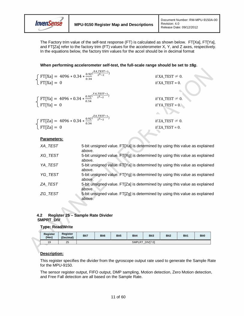
The Factory trim value of the self-test response (FT) is calculated as shown below. FT[Xa], FT[Ya], and FT[Za] refer to the factory trim (FT) values for the accelerometer X, Y, and Z axes, respectively. In the equations below, the factory trim values for the accel should be in decimal format
When performing accelerometer self-test, the full-scale range should be set to ±8g.
FT[Xa] = 4096 ∗ 0.34 ∗ 0.920.34
(𝑋𝐴_𝑇𝐸𝑆𝑇−125−2 )
if XA_TEST ≠ 0. FT[Xa] = 0 if XA_TEST = 0.
FT[Ya] = 4096 ∗ 0.34 ∗ 0.920.34
(𝑌𝐴_𝑇𝐸𝑆𝑇−125−2 )
if YA_TEST ≠ 0. FT[Ya] = 0 if YA_TEST = 0.
FT[Za] = 4096 ∗ 0.34 ∗ 0.920.34
(𝑍𝐴_𝑇𝐸𝑆𝑇−125−2 )
if ZA_TEST ≠ 0. FT[Za] = 0 if ZA_TEST = 0.
XA_TEST 5-bit unsigned value. FT[Xa] is determined by using this value as explained above.
Parameters:
XG_TEST 5-bit unsigned value. FT[Xg] is determined by using this value as explained above.
YA_TEST 5-bit unsigned value. FT[Ya] is determined by using this value as explained above.
YG_TEST 5-bit unsigned value. FT[Yg] is determined by using this value as explained above.
ZA_TEST 5-bit unsigned value. FT[Za] is determined by using this value as explained above.
ZG_TEST 5-bit unsigned value. FT[Zg] is determined by using this value as explained above.
4.2 Register 25 – Sample Rate Divider SMPRT_DIV
Type: Read/Write Register
(Hex) Register (Decimal) Bit7 Bit6 Bit5 Bit4 Bit3 Bit2 Bit1 Bit0
19 25 SMPLRT_DIV[7:0]
This register specifies the divider from the gyroscope output rate used to generate the Sample Rate for the MPU-9150.
Description:
The sensor register output, FIFO output, DMP sampling, Motion detection, Zero Motion detection, and Free Fall detection are all based on the Sample Rate.
MPU-9150 Register Map and Descriptions
Document Number: RM-MPU-9150A-00 Revision: 4.0 Release Date: 09/12/2012
12 of 60
The Sample Rate is generated by dividing the gyroscope output rate by SMPLRT_DIV:
Sample Rate = Gyroscope Output Rate / (1 + SMPLRT_DIV)
where Gyroscope Output Rate = 8kHz when the DLPF is disabled (DLPF_CFG = 0 or 7), and 1kHz when the DLPF is enabled (see Register 26).
Note:
For a diagram of the gyroscope and accelerometer signal paths, see Section 8 of the MPU-9150 Product Specification document.
The accelerometer output rate is 1kHz. This means that for a Sample Rate greater than 1kHz, the same accelerometer sample may be output to the FIFO, DMP, and sensor registers more than once.
SMPLRT_DIV 8-bit unsigned value. The Sample Rate is determined by dividing the gyroscope output rate by this value.
Parameters:

MPU-9150 Register Map and Descriptions
Document Number: RM-MPU-9150A-00 Revision: 4.0 Release Date: 09/12/2012
13 of 60
4.3 Register 26 – Configuration CONFIG
Type: Read/Write Register
(Hex) Register (Decimal) Bit7 Bit6 Bit5 Bit4 Bit3 Bit2 Bit1 Bit0
1A 26 - - EXT_SYNC_SET[2:0] DLPF_CFG[2:0]
This register configures the external Frame Synchronization (FSYNC) pin sampling and the Digital Low Pass Filter (DLPF) setting for both the gyroscopes and accelerometers.
Description:
An external signal connected to the FSYNC pin can be sampled by configuring EXT_SYNC_SET.
Signal changes to the FSYNC pin are latched so that short strobes may be captured. The latched FSYNC signal will be sampled at the Sampling Rate, as defined in register 25. After sampling, the latch will reset to the current FSYNC signal state.
The sampled value will be reported in place of the least significant bit in a sensor data register determined by the value of EXT_SYNC_SET according to the following table.
EXT_SYNC_SET FSYNC Bit Location 0 Input disabled 1 TEMP_OUT_L[0] 2 GYRO_XOUT_L[0] 3 GYRO_YOUT_L[0] 4 GYRO_ZOUT_L[0] 5 ACCEL_XOUT_L[0] 6 ACCEL_YOUT_L[0] 7 ACCEL_ZOUT_L[0]
The DLPF is configured by DLPF_CFG. The accelerometer and gyroscope are filtered according to the value of DLPF_CFG as shown in the table below.
DLPF_CFG Accelerometer (Fs = 1kHz)
Gyroscope
Bandwidth (Hz)
Delay (ms)
Bandwidth (Hz)
Delay (ms)
Fs (kHz)
0 260 0 256 0.98 8 1 184 2.0 188 1.9 1 2 94 3.0 98 2.8 1 3 44 4.9 42 4.8 1 4 21 8.5 20 8.3 1 5 10 13.8 10 13.4 1 6 5 19.0 5 18.6 1 7 RESERVED RESERVED 8
Bit 7 and bit 6 are reserved.
EXT_SYNC_SET 3-bit unsigned value. Configures the FSYNC pin sampling.
Parameters:
DLPF_CFG 3-bit unsigned value. Configures the DLPF setting.

MPU-9150 Register Map and Descriptions
Document Number: RM-MPU-9150A-00 Revision: 4.0 Release Date: 09/12/2012
14 of 60
4.4 Register 27 – Gyroscope Configuration GYRO_CONFIG
Type: Read/Write Register
(Hex) Register (Decimal) Bit7 Bit6 Bit5 Bit4 Bit3 Bit2 Bit1 Bit0
1B 27 XG_ST YG_ST ZG_ST FS_SEL[1:0] - - -
This register is used to trigger gyroscope self-test and configure the gyroscopes’ full scale range.
Description:
The self-test for each gyroscope axis can be activated by controlling the XG_ST, YG_ST, and ZG_ST bits of this register. Self-test for each axis may be performed independently or all at the same time. Please refer to registers 13 – 16 for further information on gyroscope self-test.
This register is used to configure the gyroscopes’ full scale range.
FS_SEL selects the full scale range of the gyroscope outputs according to the following table.
FS_SEL Full Scale Range 0 ± 250 °/s 1 ± 500 °/s 2 ± 1000 °/s 3 ± 2000 °/s
Bits 7 through 5 and 2 through 0 are reserved.
FS_SEL 2-bit unsigned value. Selects the full scale range of gyroscopes.
Parameters:
MPU-9150 Register Map and Descriptions
Document Number: RM-MPU-9150A-00 Revision: 4.0 Release Date: 09/12/2012
15 of 60
4.5 Register 28 – Accelerometer Configuration ACCEL_CONFIG
Type: Read/Write Register
(Hex) Register (Decimal) Bit7 Bit6 Bit5 Bit4 Bit3 Bit2 Bit1 Bit0
1C 28 XA_ST YA_ST ZA_ST AFS_SEL[1:0] ACCEL_HPF[2:0]-
This register is used to trigger accelerometer self test and configure the accelerometer full scale range.
Description:
The self-test for each accelerometer axis can be activated by controlling the XA_ST, YA_ST, and ZA_ST bits of this register. Self-test for each axis may be performed independently or all at the same time. Please refer to registers 13 – 16 for further information on accelerometer self-test.
This register also configures the Digital High Pass Filter (DHPF).
AFS_SEL selects the full scale range of the accelerometer outputs according to the following table.
AFS_SEL Full Scale Range 0 ± 2g 1 ± 4g 2 ± 8g 3 ± 16g
ACCEL_HPF configures the DHPF available in the path leading to motion detectors (Free Fall, Motion threshold, and Zero Motion). The high pass filter output is not available to the data registers (see Figure in Section 8 of the MPU-9150 Product Specification document).
The high pass filter has three modes:
• Reset: The filter output settles to zero within one sample. This effectively disables the high pass filter. This mode may be toggled to quickly settle the filter.
• On: The high pass filter will pass signals above the cut off frequency. • Hold: When triggered, the filter holds the present sample. The filter output will be the
difference between the input sample and the held sample.
ACCEL_HPF Filter Mode Cut-off Frequency 0 Reset None 1 On 5Hz 2 On 2.5Hz 3 On 1.25Hz 4 On 0.63Hz 7 Hold None
XA_ST When set to 1, the X- Axis accelerometer performs self-test.
Parameters:
YA_ST When set to 1, the Y- Axis accelerometer performs self-test.
ZA_ST When set to 1, the Z- Axis accelerometer performs self-test.
ACCEL_FS_SEL 2-bit unsigned value. Selects the full scale range of accelerometers.
ACCEL_HPF 3-bit unsigned value. Selects the Digital High Pass Filter configuration.
MPU-9150 Register Map and Descriptions
Document Number: RM-MPU-9150A-00 Revision: 4.0 Release Date: 09/12/2012
16 of 60
4.6 Register 29 – Free Fall Acceleration Threshold FF_THR
Type: Read/Write Register
(Hex) Register (Decimal) Bit7 Bit6 Bit5 Bit4 Bit3 Bit2 Bit1 Bit0
1D 29 FF_THR[7:0]
This register configures the detection threshold for Free Fall event detection. The mg per LSB increment for FF_THR can be found in the Electrical Specifications table of the MPU-9150 Product Specification document.
Description:
Free Fall is detected when the absolute value of the accelerometer measurements for the three axes are each less than the detection threshold. This condition increments the Free Fall duration counter (Register 30). The Free Fall interrupt is triggered when the Free Fall duration counter reaches the time specified in FF_DUR (Register 30).
For more details on the Free Fall detection interrupt, see Section 8.2 of the MPU-9150 Product Specification document as well as Registers 56 and 58 of this document.
FF_THR 8-bit unsigned value specifying the Free Fall detection threshold.
Parameters:
4.7 Register 30 – Free Fall Duration FF_DUR
Type: Read/Write Register
(Hex) Register (Decimal) Bit7 Bit6 Bit5 Bit4 Bit3 Bit2 Bit1 Bit0
1E 30 FF_DUR[7:0]
This register configures the duration counter threshold for Free Fall event detection. The duration counter ticks at 1kHz, therefore FF_DUR has a unit of 1 LSB = 1 ms.
Description:
The Free Fall duration counter increments while the absolute value of the accelerometer measurements are each less than the detection threshold (Register 29). The Free Fall interrupt is triggered when the Free Fall duration counter reaches the time specified in this register.
For more details on the Free Fall detection interrupt, see Section 8.2 of the MPU-9150 Product Specification document as well as Registers 56 and 58 of this document.
FF_DUR 8-bit unsigned value. Specifies the duration counter threshold. Unit of LSB = 1ms.
Parameters:
MPU-9150 Register Map and Descriptions
Document Number: RM-MPU-9150A-00 Revision: 4.0 Release Date: 09/12/2012
17 of 60
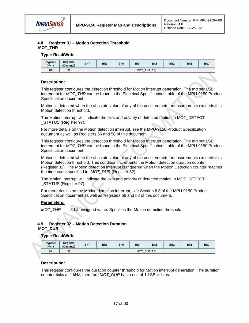
4.8 Register 31 – Motion Detection Threshold MOT_THR
Type: Read/Write Register
(Hex) Register (Decimal) Bit7 Bit6 Bit5 Bit4 Bit3 Bit2 Bit1 Bit0
1F 31 MOT_THR[7:0]
This register configures the detection threshold for Motion interrupt generation. The mg per LSB increment for MOT_THR can be found in the Electrical Specifications table of the MPU-9150 Product Specification document.
Description:
Motion is detected when the absolute value of any of the accelerometer measurements exceeds this Motion detection threshold.
The Motion interrupt will indicate the axis and polarity of detected motion in MOT_DETECT _STATUS (Register 97).
For more details on the Motion detection interrupt, see the MPU-9150 Product Specification document as well as Registers 56 and 58 of this document.
This register configures the detection threshold for Motion interrupt generation. The mg per LSB increment for MOT_THR can be found in the Electrical Specifications table of the MPU-9150 Product Specification document.
Motion is detected when the absolute value of any of the accelerometer measurements exceeds this Motion detection threshold. This condition increments the Motion detection duration counter (Register 32). The Motion detection interrupt is triggered when the Motion Detection counter reaches the time count specified in MOT_DUR (Register 32).
The Motion interrupt will indicate the axis and polarity of detected motion in MOT_DETECT _STATUS (Register 97).
For more details on the Motion detection interrupt, see Section 8.3 of the MPU-9150 Product Specification document as well as Registers 56 and 58 of this document.
MOT_THR 8-bit unsigned value. Specifies the Motion detection threshold.
Parameters:
4.9 Register 32 – Motion Detection Duration MOT_DUR
Type: Read/Write Register
(Hex) Register (Decimal) Bit7 Bit6 Bit5 Bit4 Bit3 Bit2 Bit1 Bit0
20 32 MOT_DUR[7:0]
This register configures the duration counter threshold for Motion interrupt generation. The duration counter ticks at 1 kHz, therefore MOT_DUR has a unit of 1 LSB = 1 ms.
Description:
MPU-9150 Register Map and Descriptions
Document Number: RM-MPU-9150A-00 Revision: 4.0 Release Date: 09/12/2012
18 of 60
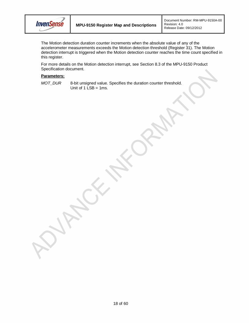
The Motion detection duration counter increments when the absolute value of any of the accelerometer measurements exceeds the Motion detection threshold (Register 31). The Motion detection interrupt is triggered when the Motion detection counter reaches the time count specified in this register.
For more details on the Motion detection interrupt, see Section 8.3 of the MPU-9150 Product Specification document.
MOT_DUR 8-bit unsigned value. Specifies the duration counter threshold. Unit of 1 LSB = 1ms.
Parameters:

MPU-9150 Register Map and Descriptions
Document Number: RM-MPU-9150A-00 Revision: 4.0 Release Date: 09/12/2012
19 of 60
4.10 Register 33 – Zero Motion Detection Threshold ZRMOT_THR
Type: Read/Write Register
(Hex) Register (Decimal) Bit7 Bit6 Bit5 Bit4 Bit3 Bit2 Bit1 Bit0
21 33 ZRMOT_THR[7:0]
This register configures the detection threshold for Zero Motion interrupt generation. The mg per LSB increment for ZRMOT_THR can be found in the Electrical Specifications table of the MPU-9150 Product Specification document.
Description:
Zero Motion is detected when the absolute value of the accelerometer measurements for the 3 axes are each less than the detection threshold. This condition increments the Zero Motion duration counter (Register 34). The Zero Motion interrupt is triggered when the Zero Motion duration counter reaches the time count specified in ZRMOT_DUR (Register 34).
Unlike Free Fall or Motion detection, Zero Motion detection triggers an interrupt both when Zero Motion is first detected and when Zero Motion is no longer detected.
When a zero motion event is detected, a Zero Motion Status will be indicated in the MOT_DETECT_STATUS register (Register 97). When a motion-to-zero-motion condition is detected, the status bit is set to 1. When a zero-motion-to-motion condition is detected, the status bit is set to 0.
For more details on the Zero Motion detection interrupt, see Section 8.4 of the MPU-9150 Product Specification document as well as Registers 56 and 58 of this document.
ZRMOT_THR 8-bit unsigned value. Specifies the Zero Motion detection threshold.
Parameters:
4.11 Register 34 – Zero Motion Detection Duration ZRMOT_DUR
Type: Read/Write Register
(Hex) Register (Decimal) Bit7 Bit6 Bit5 Bit4 Bit3 Bit2 Bit1 Bit0
22 34 ZRMOT_DUR[7:0]
This register configures the duration counter threshold for Zero Motion interrupt generation. The duration counter ticks at 16 Hz, therefore ZRMOT_DUR has a unit of 1 LSB = 64 ms.
Description:
The Zero Motion duration counter increments while the absolute value of the accelerometer measurements are each less than the detection threshold (Register 33). The Zero Motion interrupt is triggered when the Zero Motion duration counter reaches the time count specified in this register.
For more details on the Zero Motion detection interrupt, see Section 8.4 of the MPU-9150 Product Specification document, as well as Registers 56 and 58 of this document.
ZRMOT_DUR 8-bit unsigned value. Specifies the duration counter threshold. Unit of 1 LSB = 64ms.
Parameters:
MPU-9150 Register Map and Descriptions
Document Number: RM-MPU-9150A-00 Revision: 4.0 Release Date: 09/12/2012
20 of 60
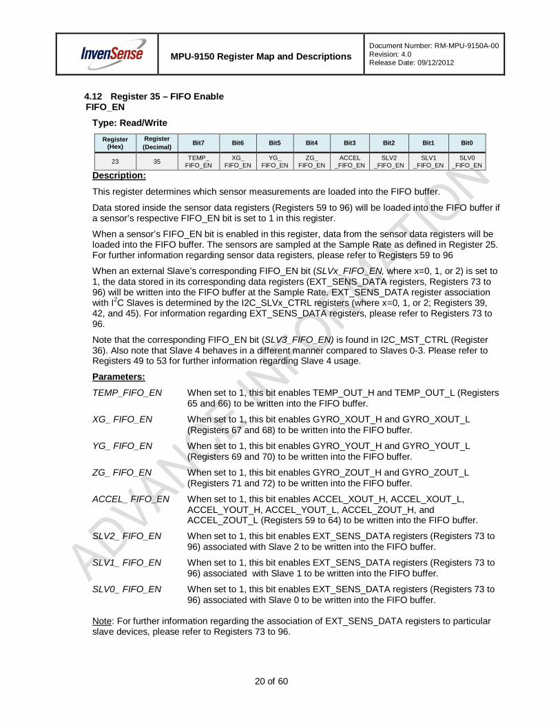
4.12 Register 35 – FIFO Enable FIFO_EN
Type: Read/Write Register
(Hex) Register (Decimal) Bit7 Bit6 Bit5 Bit4 Bit3 Bit2 Bit1 Bit0
23 35 TEMP_ FIFO_EN
XG_ FIFO_EN
YG_ FIFO_EN
ZG_ FIFO_EN
ACCEL _FIFO_EN
SLV2 _FIFO_EN
SLV1 _FIFO_EN
SLV0 _FIFO_EN
This register determines which sensor measurements are loaded into the FIFO buffer.
Description:
Data stored inside the sensor data registers (Registers 59 to 96) will be loaded into the FIFO buffer if a sensor’s respective FIFO_EN bit is set to 1 in this register.
When a sensor’s FIFO_EN bit is enabled in this register, data from the sensor data registers will be loaded into the FIFO buffer. The sensors are sampled at the Sample Rate as defined in Register 25. For further information regarding sensor data registers, please refer to Registers 59 to 96
When an external Slave’s corresponding FIFO_EN bit (SLVx_FIFO_EN, where x=0, 1, or 2) is set to 1, the data stored in its corresponding data registers (EXT_SENS_DATA registers, Registers 73 to 96) will be written into the FIFO buffer at the Sample Rate. EXT_SENS_DATA register association with I2C Slaves is determined by the I2C_SLVx_CTRL registers (where x=0, 1, or 2; Registers 39, 42, and 45). For information regarding EXT_SENS_DATA registers, please refer to Registers 73 to 96.
Note that the corresponding FIFO_EN bit (SLV3_FIFO_EN) is found in I2C_MST_CTRL (Register 36). Also note that Slave 4 behaves in a different manner compared to Slaves 0-3. Please refer to Registers 49 to 53 for further information regarding Slave 4 usage.
TEMP_FIFO_EN When set to 1, this bit enables TEMP_OUT_H and TEMP_OUT_L (Registers 65 and 66) to be written into the FIFO buffer.
Parameters:
XG_ FIFO_EN When set to 1, this bit enables GYRO_XOUT_H and GYRO_XOUT_L (Registers 67 and 68) to be written into the FIFO buffer.
YG_ FIFO_EN When set to 1, this bit enables GYRO_YOUT_H and GYRO_YOUT_L (Registers 69 and 70) to be written into the FIFO buffer.
ZG_ FIFO_EN When set to 1, this bit enables GYRO_ZOUT_H and GYRO_ZOUT_L (Registers 71 and 72) to be written into the FIFO buffer.
ACCEL_ FIFO_EN When set to 1, this bit enables ACCEL_XOUT_H, ACCEL_XOUT_L, ACCEL_YOUT_H, ACCEL_YOUT_L, ACCEL_ZOUT_H, and ACCEL_ZOUT_L (Registers 59 to 64) to be written into the FIFO buffer.
SLV2_ FIFO_EN When set to 1, this bit enables EXT_SENS_DATA registers (Registers 73 to 96) associated with Slave 2 to be written into the FIFO buffer.
SLV1_ FIFO_EN When set to 1, this bit enables EXT_SENS_DATA registers (Registers 73 to 96) associated with Slave 1 to be written into the FIFO buffer.
SLV0_ FIFO_EN When set to 1, this bit enables EXT_SENS_DATA registers (Registers 73 to 96) associated with Slave 0 to be written into the FIFO buffer.
Note: For further information regarding the association of EXT_SENS_DATA registers to particular slave devices, please refer to Registers 73 to 96.
MPU-9150 Register Map and Descriptions
Document Number: RM-MPU-9150A-00 Revision: 4.0 Release Date: 09/12/2012
21 of 60
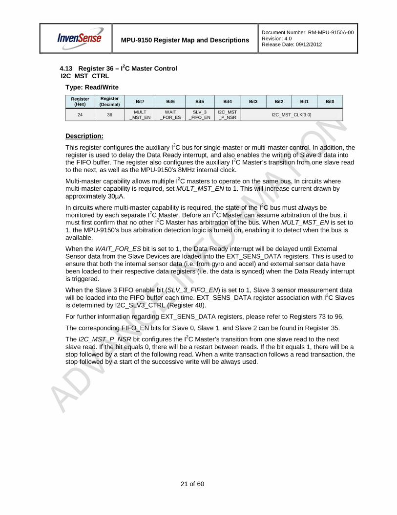
4.13 Register 36 – I2C Master Control I2C_MST_CTRL
Type: Read/Write Register
(Hex) Register (Decimal) Bit7 Bit6 Bit5 Bit4 Bit3 Bit2 Bit1 Bit0
24 36 MULT _MST_EN
WAIT _FOR_ES
SLV_3 _FIFO_EN
I2C_MST _P_NSR I2C_MST_CLK[3:0]
This register configures the auxiliary I2C bus for single-master or multi-master control. In addition, the register is used to delay the Data Ready interrupt, and also enables the writing of Slave 3 data into the FIFO buffer. The register also configures the auxiliary I2C Master’s transition from one slave read to the next, as well as the MPU-9150’s 8MHz internal clock.
Description:
Multi-master capability allows multiple I2C masters to operate on the same bus. In circuits where multi-master capability is required, set MULT_MST_EN to 1. This will increase current drawn by approximately 30µA.
In circuits where multi-master capability is required, the state of the I2C bus must always be monitored by each separate I2C Master. Before an I2C Master can assume arbitration of the bus, it must first confirm that no other I2C Master has arbitration of the bus. When MULT_MST_EN is set to 1, the MPU-9150’s bus arbitration detection logic is turned on, enabling it to detect when the bus is available.
When the WAIT_FOR_ES bit is set to 1, the Data Ready interrupt will be delayed until External Sensor data from the Slave Devices are loaded into the EXT_SENS_DATA registers. This is used to ensure that both the internal sensor data (i.e. from gyro and accel) and external sensor data have been loaded to their respective data registers (i.e. the data is synced) when the Data Ready interrupt is triggered.
When the Slave 3 FIFO enable bit (SLV_3_FIFO_EN) is set to 1, Slave 3 sensor measurement data will be loaded into the FIFO buffer each time. EXT_SENS_DATA register association with I2C Slaves is determined by I2C_SLV3_CTRL (Register 48).
For further information regarding EXT_SENS_DATA registers, please refer to Registers 73 to 96.
The corresponding FIFO_EN bits for Slave 0, Slave 1, and Slave 2 can be found in Register 35.
The I2C_MST_P_NSR bit configures the I2C Master’s transition from one slave read to the next slave read. If the bit equals 0, there will be a restart between reads. If the bit equals 1, there will be a stop followed by a start of the following read. When a write transaction follows a read transaction, the stop followed by a start of the successive write will be always used.
MPU-9150 Register Map and Descriptions
Document Number: RM-MPU-9150A-00 Revision: 4.0 Release Date: 09/12/2012
22 of 60
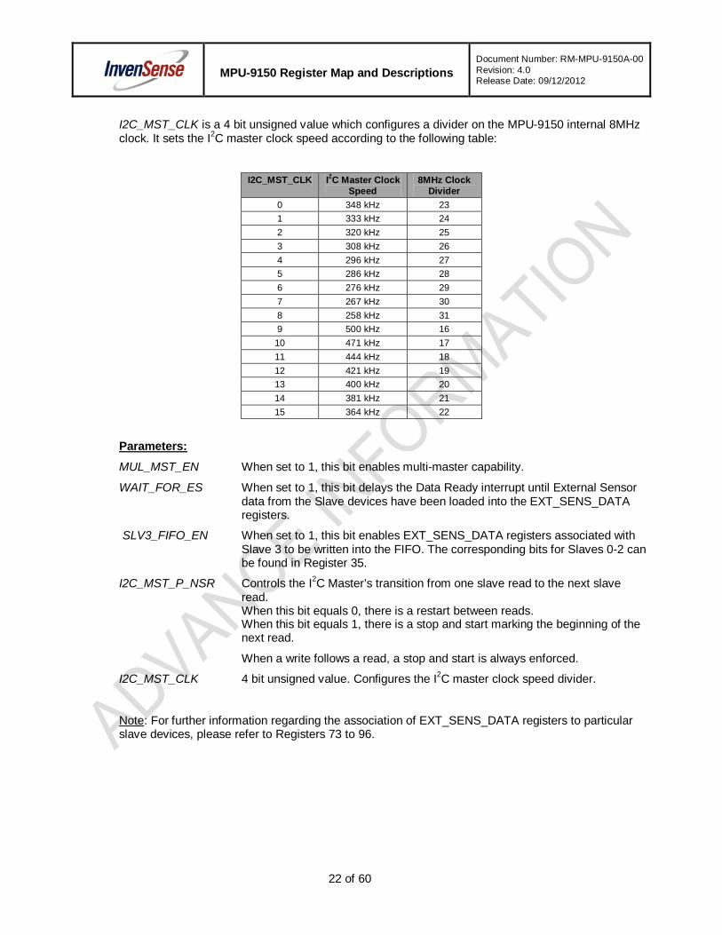
I2C_MST_CLK is a 4 bit unsigned value which configures a divider on the MPU-9150 internal 8MHz clock. It sets the I2C master clock speed according to the following table:
I2C_MST_CLK I2C Master Clock Speed
8MHz Clock Divider
0 348 kHz 23 1 333 kHz 24 2 320 kHz 25 3 308 kHz 26 4 296 kHz 27 5 286 kHz 28 6 276 kHz 29 7 267 kHz 30 8 258 kHz 31 9 500 kHz 16 10 471 kHz 17 11 444 kHz 18 12 421 kHz 19 13 400 kHz 20 14 381 kHz 21 15 364 kHz 22
MUL_MST_EN When set to 1, this bit enables multi-master capability.
Parameters:
WAIT_FOR_ES When set to 1, this bit delays the Data Ready interrupt until External Sensor data from the Slave devices have been loaded into the EXT_SENS_DATA registers.
SLV3_FIFO_EN When set to 1, this bit enables EXT_SENS_DATA registers associated with Slave 3 to be written into the FIFO. The corresponding bits for Slaves 0-2 can be found in Register 35.
I2C_MST_P_NSR Controls the I2C Master’s transition from one slave read to the next slave read. When this bit equals 0, there is a restart between reads. When this bit equals 1, there is a stop and start marking the beginning of the next read.
When a write follows a read, a stop and start is always enforced.
I2C_MST_CLK 4 bit unsigned value. Configures the I2C master clock speed divider.
Note
: For further information regarding the association of EXT_SENS_DATA registers to particular slave devices, please refer to Registers 73 to 96.

MPU-9150 Register Map and Descriptions
Document Number: RM-MPU-9150A-00 Revision: 4.0 Release Date: 09/12/2012
23 of 60
4.14 Registers 37 to 39 – I2C Slave 0 Control I2C_SLV0_ADDR, I2C_SLV0_REG, and I2C_SLV0_CTRL
Type: Read/Write
Register (Hex)
Register (Decimal) Bit7 Bit6 Bit5 Bit4 Bit3 Bit2 Bit1 Bit0
25 37 I2C_SLV0 _RW I2C_SLV0_ADDR[6:0]
26 38 I2C_SLV0_REG[7:0]
27 39 I2C_SLV0 _EN
I2C_SLV0 _BYTE _SW
I2C_SLV0_REG_DIS
I2C_SLV0_GRP I2C_SLV0_LEN[3:0]
These registers configure the data transfer sequence for Slave 0. Slaves 1, 2, and 3 also behave in a similar manner to Slave 0. However, Slave 4’s characteristics differ greatly from those of Slaves 0-3. For further information regarding Slave 4, please refer to registers 49 to 53.
Description:
I2C slave data transactions between the MPU-9150 and Slave 0 are set as either read or write operations by the I2C_SLV0_RW bit. When this bit is 1, the transfer is a read operation. When the bit is 0, the transfer is a write operation.
I2C_SLV0_ADDR is used to specify the I2C slave address of Slave 0.
Data transfer starts at an internal register within Slave 0. This address of this register is specified by I2C_SLV0_REG.
The number of bytes transferred is specified by I2C_SLV0_LEN. When more than 1 byte is transferred (I2C_SLV0_LEN > 1), data is read from (written to) sequential addresses starting from I2C_SLV0_REG.
In read mode, the result of the read is placed in the lowest available EXT_SENS_DATA register. For further information regarding the allocation of read results, please refer to the EXT_SENS_DATA register description (Registers 73 – 96).
In write mode, the contents of I2C_SLV0_DO (Register 99) will be written to the slave device.
I2C_SLV0_EN enables Slave 0 for I2C data transaction. A data transaction is performed only if more than zero bytes are to be transferred (I2C_SLV0_LEN > 0) between an enabled slave device (I2C_SLV0_EN = 1).
I2C_SLV0_BYTE_SW configures byte swapping of word pairs. When byte swapping is enabled, the high and low bytes of a word pair are swapped. Please refer to I2C_SLV0_GRP for the pairing convention of the word pairs. When this bit is cleared to 0, bytes transferred to and from Slave 0 will be written to EXT_SENS_DATA registers in the order they were transferred.
When I2C_SLV0_REG_DIS is set to 1, the transaction will read or write data only. When cleared to 0, the transaction will write a register address prior to reading or writing data. This bit should equal 0 when specifying the register address within the Slave device to/from which the ensuing data transaction will take place.

MPU-9150 Register Map and Descriptions
Document Number: RM-MPU-9150A-00 Revision: 4.0 Release Date: 09/12/2012
24 of 60
I2C_SLV0_GRP specifies the grouping order of word pairs received from registers. When cleared to 0, bytes from register addresses 0 and 1, 2 and 3, etc (even, then odd register addresses) are paired to form a word. When set to 1, bytes from register addresses are paired 1 and 2, 3 and 4, etc. (odd, then even register addresses) are paired to form a word.
I2C data transactions are performed at the Sample Rate, as defined in Register 25. The user is responsible for ensuring that I2C data transactions to and from each enabled Slave can be completed within a single period of the Sample Rate.
The I2C slave access rate can be reduced relative to the Sample Rate. This reduced access rate is determined by I2C_MST_DLY (Register 52). Whether a slave’s access rate is reduced relative to the Sample Rate is determined by I2C_MST_DELAY_CTRL (Register 103). The processing order for the slaves is fixed. The sequence followed for processing the slaves is Slave 0, Slave 1, Slave 2, Slave 3 and Slave 4. If a particular Slave is disabled it will be skipped. Each slave can either be accessed at the sample rate or at a reduced sample rate. In a case where some slaves are accessed at the Sample Rate and some slaves are accessed at the reduced rate, the sequence of accessing the slaves (Slave 0 to Slave 4) is still followed. However, the reduced rate slaves will be skipped if their access rate dictates that they should not be accessed during that particular cycle. For further information regarding the reduced access rate, please refer to Register 52. Whether a slave is accessed at the Sample Rate or at the reduced rate is determined by the Delay Enable bits in Register 103.
I2C_SLV0_RW When set to 1, this bit configures the data transfer as a read operation.
Parameters:
When cleared to 0, this bit configures the data transfer as a write operation. I2C_SLV0_ADDR 7-bit I2C address of Slave 0.
I2C_SLV0_REG 8-bit address of the Slave 0 register to/from which data transfer starts.
I2C_SLV0_EN When set to 1, this bit enables Slave 0 for data transfer operations. When cleared to 0, this bit disables Slave 0 from data transfer operations.
I2C_SLV0_BYTE_SW When set to 1, this bit enables byte swapping. When byte swapping is enabled, the high and low bytes of a word pair are swapped. Please refer to I2C_SLV0_GRP for the pairing convention of the word pairs.
When cleared to 0, bytes transferred to and from Slave 0 will be written to EXT_SENS_DATA registers in the order they were transferred.
I2C_SLV0_REG_DIS When set to 1, the transaction will read or write data only. When cleared to 0, the transaction will write a register address prior to reading or writing data.
I2C_SLV0_GRP 1-bit value specifying the grouping order of word pairs received from registers. When cleared to 0, bytes from register addresses 0 and 1, 2 and 3, etc (even, then odd register addresses) are paired to form a word. When set to 1, bytes from register addresses are paired 1 and 2, 3 and 4, etc. (odd, then even register addresses) are paired to form a word.
I2C_SLV0_LEN 4-bit unsigned value. Specifies the number of bytes transferred to and from Slave 0. Clearing this bit to 0 is equivalent to disabling the register by writing 0 to I2C_SLV0_EN.
MPU-9150 Register Map and Descriptions
Document Number: RM-MPU-9150A-00 Revision: 4.0 Release Date: 09/12/2012
25 of 60
Byte Swapping ExampleThe following example demonstrates byte swapping for I2C_SLV0_BYTE_SW = 1, I2C_SLV0_GRP = 0, I2C_SLV0_REG = 0x01, and I2C_SLV0_LEN = 0x4:
1. The first byte, read from Slave 0 register 0x01, will be stored at EXT_SENS_DATA_00. Because I2C_SLV0_GRP = 0, bytes from even, then odd register addresses will be paired together as word pairs. Since the read operation started from an odd register address instead of an even address, only one byte is read.
2. The second and third bytes will be swapped, since I2C_SLV0_BYTE_SW = 1 and I2C_SLV0_REG[0] = 1. The data read from 0x02 will be stored at EXT_SENS_DATA_02, and the data read from 0x03 will be stored at EXT_SENS_DATA_01.
3. The last byte, read from address 0x04, will be stored at EXT_SENS_DATA_03. Because there is only one byte remaining in the read operation, byte swapping will not occur.
Slave 0 is accessed at the Sample Rate, while Slave 1 is accessed at half the Sample Rate. The other slaves are disabled. In the first cycle, both Slave 0 and Slave 1 will be accessed. However, in the second cycle, only Slave 0 will be accessed. In the third cycle, both Slave 0 and Slave 1 will be accessed. In the fourth cycle, only Slave 0 will be accessed. This pattern continues.
Slave Access Example

MPU-9150 Register Map and Descriptions
Document Number: RM-MPU-9150A-00 Revision: 4.0 Release Date: 09/12/2012
26 of 60
4.15 Registers 40 to 42 – I2C Slave 1 Control I2C_SLV1_ADDR, I2C_SLV1_REG, and I2C_SLV1_CTRL
Type: Read/Write Register
(Hex) Register (Decimal) Bit7 Bit6 Bit5 Bit4 Bit3 Bit2 Bit1 Bit0
28 40 I2C_SLV1 _RW I2C_SLV1_ADDR[6:0]
29 41 I2C_SLV1_REG[7:0]
2A 42 I2C_SLV1 _EN
I2C_SLV1 _BYTE _SW
I2C_SLV1_REG_DIS
I2C_SLV1_GRP I2C_SLV1_LEN[3:0]
These registers describe the data transfer sequence for Slave 1. Their functions correspond to those described for the Slave 0 registers (Registers 37 to 39).
Description:
4.16 Registers 43 to 45 – I2C Slave 2 Control I2C_SLV2_ADDR, I2C_SLV2_REG, and I2C_SLV2_CTRL
Type: Read/Write Register
(Hex) Register (Decimal) Bit7 Bit6 Bit5 Bit4 Bit3 Bit2 Bit1 Bit0
2B 43 I2C_SLV2 _RW I2C_SLV2_ADDR[6:0]
2C 44 I2C_SLV2_REG[7:0]
2D 45 I2C_SLV2 _EN
I2C_SLV2 _BYTE _SW
I2C_SLV2_REG_DIS
I2C_SLV2_GRP I2C_SLV2_LEN[3:0]
These registers describe the data transfer sequence for Slave 2. Their functions correspond to those described for the Slave 0 registers (Registers 37 to 39).
Description:
4.17 Registers 46 to 48 – I2C Slave 3 Control I2C_SLV3_ADDR, I2C_SLV3_REG, and I2C_SLV3_CTRL
Type: Read/Write Register
(Hex) Register (Decimal) Bit7 Bit6 Bit5 Bit4 Bit3 Bit2 Bit1 Bit0
2E 46 I2C_SLV3 _RW I2C_SLV3_ADDR[6:0]
2F 47 I2C_SLV3_REG[7:0]
30 48 I2C_SLV3 _EN
I2C_SLV3 _BYTE _SW
I2C_SLV3_REG_DIS
I2C_SLV3_GRP I2C_SLV3_LEN[3:0]
These registers describe the data transfer sequence for Slave 3. Their functions correspond to those described for the Slave 0 registers (Registers 37 to 39).
Description:
MPU-9150 Register Map and Descriptions
Document Number: RM-MPU-9150A-00 Revision: 4.0 Release Date: 09/12/2012
27 of 60
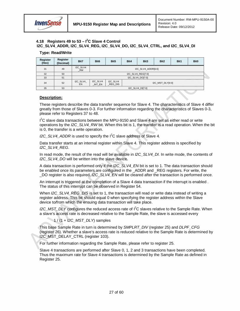
4.18 Registers 49 to 53 – I2C Slave 4 Control I2C_SLV4_ADDR, I2C_SLV4_REG, I2C_SLV4_DO, I2C_SLV4_CTRL, and I2C_SLV4_DI
Type: Read/Write Register
(Hex) Register (Decimal) Bit7 Bit6 Bit5 Bit4 Bit3 Bit2 Bit1 Bit0
31 49 I2C_SLV4 _RW I2C_SLV4_ADDR[6:0]
32 50 I2C_SLV4_REG[7:0] 33 51 I2C_SLV4_DO[7:0]
34 52 I2C_SLV4_EN
I2C_SLV4 _INT_EN
I2C_SLV4 _REG_DIS I2C_MST_DLY[4:0]
35 53 I2C_SLV4_DI[7:0]
These registers describe the data transfer sequence for Slave 4. The characteristics of Slave 4 differ greatly from those of Slaves 0-3. For further information regarding the characteristics of Slaves 0-3, please refer to Registers 37 to 48.
Description:
I2C slave data transactions between the MPU-9150 and Slave 4 are set as either read or write operations by the I2C_SLV4_RW bit. When this bit is 1, the transfer is a read operation. When the bit is 0, the transfer is a write operation.
I2C_SLV4_ADDR is used to specify the I2C slave address of Slave 4.
Data transfer starts at an internal register within Slave 4. This register address is specified by I2C_SLV4_REG.
In read mode, the result of the read will be available in I2C_SLV4_DI. In write mode, the contents of I2C_SLV4_DO will be written into the slave device.
A data transaction is performed only if the I2C_SLV4_EN bit is set to 1. The data transaction should be enabled once its parameters are configured in the _ADDR and _REG registers. For write, the _DO register is also required. I2C_SLV4_EN will be cleared after the transaction is performed once.
An interrupt is triggered at the completion of a Slave 4 data transaction if the interrupt is enabled . The status of this interrupt can be observed in Register 54.
When I2C_SLV4_REG_DIS is set to 1, the transaction will read or write data instead of writing a register address. This bit should equal 0 when specifying the register address within the Slave device to/from which the ensuing data transaction will take place.
I2C_MST_DLY configures the reduced access rate of I2C slaves relative to the Sample Rate. When a slave’s access rate is decreased relative to the Sample Rate, the slave is accessed every
1 / (1 + I2C_MST_DLY) samples
This base Sample Rate in turn is determined by SMPLRT_DIV (register 25) and DLPF_CFG (register 26). Whether a slave’s access rate is reduced relative to the Sample Rate is determined by I2C_MST_DELAY_CTRL (register 103).
For further information regarding the Sample Rate, please refer to register 25.
Slave 4 transactions are performed after Slave 0, 1, 2 and 3 transactions have been completed. Thus the maximum rate for Slave 4 transactions is determined by the Sample Rate as defined in Register 25.
MPU-9150 Register Map and Descriptions
Document Number: RM-MPU-9150A-00 Revision: 4.0 Release Date: 09/12/2012
28 of 60
I2C_SLV4_RW When set to 1, this bit configures the data transfer as a read operation. When cleared to 0, this bit configures the data transfer as a write operation.
Parameters:
I2C_SLV4_ADDR 7-bit I2C address for Slave 4.
I2C_SLV4_REG 8-bit address of the Slave 4 register to/from which data transfer starts.
I2C_SLV4_DO This register stores the data to be written into the Slave 4. If I2C_SLV4_RW is set 1 (set to read), this register has no effect.
I2C_SLV4_EN When set to 1, this bit enables Slave 4 for data transfer operations.
When cleared to 0, this bit disables Slave 4 from data transfer operations.
I2C_SLV4_INT_EN When set to 1, this bit enables the generation of an interrupt signal upon completion of a Slave 4 transaction.
When cleared to 0, this bit disables the generation of an interrupt signal upon completion of a Slave 4 transaction.
The interrupt status can be observed in Register 54.
I2C_SLV4_REG_DIS When set to 1, the transaction will read or write data. When cleared to 0, the transaction will read or write a register address.
I2C_MST_DLY Configures the decreased access rate of slave devices relative to the Sample Rate.
I2C_SLV4_DI This register stores the data read from Slave 4.
This field is populated after a read transaction.
MPU-9150 Register Map and Descriptions
Document Number: RM-MPU-9150A-00 Revision: 4.0 Release Date: 09/12/2012
29 of 60
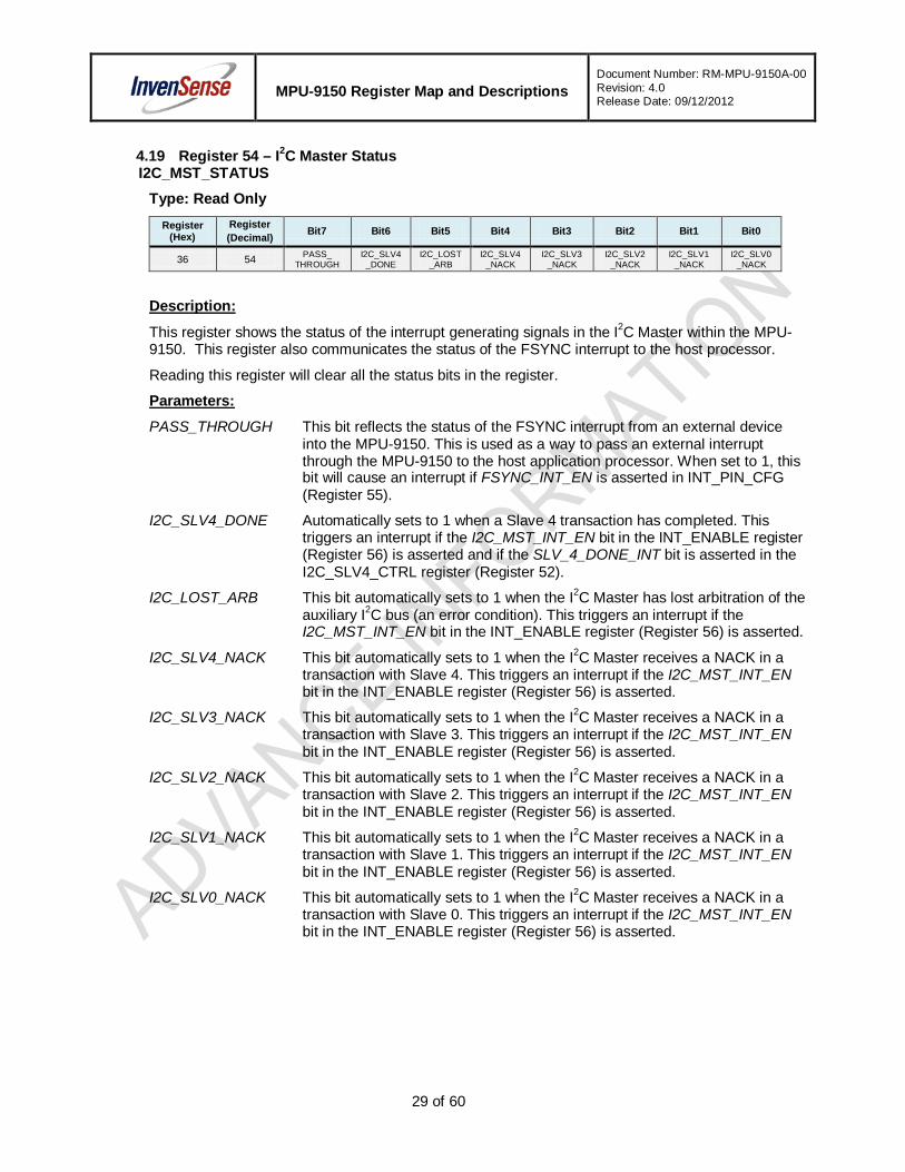
4.19 Register 54 – I2C Master Status I2C_MST_STATUS
Type: Read Only Register
(Hex) Register (Decimal) Bit7 Bit6 Bit5 Bit4 Bit3 Bit2 Bit1 Bit0
36 54 PASS_ THROUGH
I2C_SLV4_DONE
I2C_LOST_ARB
I2C_SLV4_NACK
I2C_SLV3 _NACK
I2C_SLV2 _NACK
I2C_SLV1 _NACK
I2C_SLV0_NACK
This register shows the status of the interrupt generating signals in the I2C Master within the MPU-9150. This register also communicates the status of the FSYNC interrupt to the host processor.
Description:
Reading this register will clear all the status bits in the register.
PASS_THROUGH This bit reflects the status of the FSYNC interrupt from an external device into the MPU-9150. This is used as a way to pass an external interrupt through the MPU-9150 to the host application processor. When set to 1, this bit will cause an interrupt if FSYNC_INT_EN is asserted in INT_PIN_CFG (Register 55).
Parameters:
I2C_SLV4_DONE Automatically sets to 1 when a Slave 4 transaction has completed. This triggers an interrupt if the I2C_MST_INT_EN bit in the INT_ENABLE register (Register 56) is asserted and if the SLV_4_DONE_INT bit is asserted in the I2C_SLV4_CTRL register (Register 52).
I2C_LOST_ARB This bit automatically sets to 1 when the I2C Master has lost arbitration of the auxiliary I2C bus (an error condition). This triggers an interrupt if the I2C_MST_INT_EN bit in the INT_ENABLE register (Register 56) is asserted.
I2C_SLV4_NACK This bit automatically sets to 1 when the I2C Master receives a NACK in a transaction with Slave 4. This triggers an interrupt if the I2C_MST_INT_EN bit in the INT_ENABLE register (Register 56) is asserted.
I2C_SLV3_NACK This bit automatically sets to 1 when the I2C Master receives a NACK in a transaction with Slave 3. This triggers an interrupt if the I2C_MST_INT_EN bit in the INT_ENABLE register (Register 56) is asserted.
I2C_SLV2_NACK This bit automatically sets to 1 when the I2C Master receives a NACK in a transaction with Slave 2. This triggers an interrupt if the I2C_MST_INT_EN bit in the INT_ENABLE register (Register 56) is asserted.
I2C_SLV1_NACK This bit automatically sets to 1 when the I2C Master receives a NACK in a transaction with Slave 1. This triggers an interrupt if the I2C_MST_INT_EN bit in the INT_ENABLE register (Register 56) is asserted.
I2C_SLV0_NACK This bit automatically sets to 1 when the I2C Master receives a NACK in a transaction with Slave 0. This triggers an interrupt if the I2C_MST_INT_EN bit in the INT_ENABLE register (Register 56) is asserted.
MPU-9150 Register Map and Descriptions
Document Number: RM-MPU-9150A-00 Revision: 4.0 Release Date: 09/12/2012
30 of 60
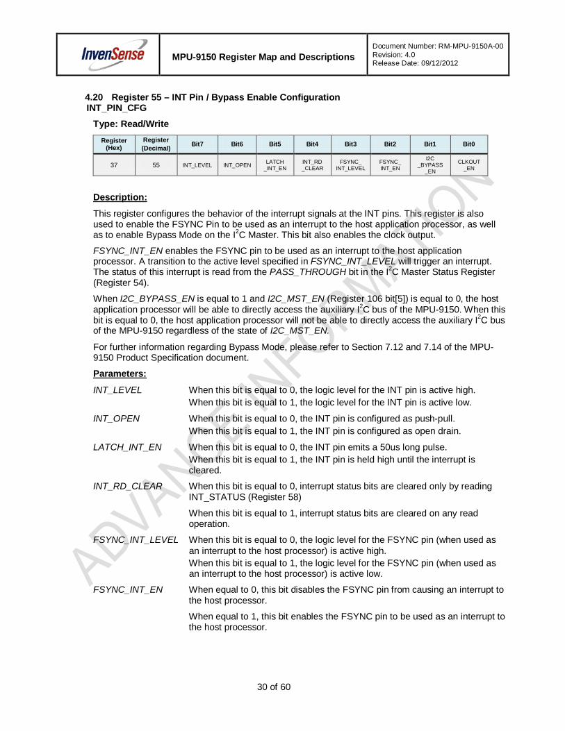
4.20 Register 55 – INT Pin / Bypass Enable Configuration INT_PIN_CFG
Type: Read/Write Register
(Hex) Register (Decimal) Bit7 Bit6 Bit5 Bit4 Bit3 Bit2 Bit1 Bit0
37 55 INT_LEVEL INT_OPEN LATCH _INT_EN
INT_RD _CLEAR
FSYNC_ INT_LEVEL
FSYNC_ INT_EN
I2C _BYPASS
_EN
CLKOUT _EN
This register configures the behavior of the interrupt signals at the INT pins. This register is also used to enable the FSYNC Pin to be used as an interrupt to the host application processor, as well as to enable Bypass Mode on the I2C Master. This bit also enables the clock output.
Description:
FSYNC_INT_EN enables the FSYNC pin to be used as an interrupt to the host application processor. A transition to the active level specified in FSYNC_INT_LEVEL will trigger an interrupt. The status of this interrupt is read from the PASS_THROUGH bit in the I2C Master Status Register (Register 54).
When I2C_BYPASS_EN is equal to 1 and I2C_MST_EN (Register 106 bit[5]) is equal to 0, the host application processor will be able to directly access the auxiliary I2C bus of the MPU-9150. When this bit is equal to 0, the host application processor will not be able to directly access the auxiliary I2C bus of the MPU-9150 regardless of the state of I2C_MST_EN.
For further information regarding Bypass Mode, please refer to Section 7.12 and 7.14 of the MPU-9150 Product Specification document.
INT_LEVEL When this bit is equal to 0, the logic level for the INT pin is active high.
Parameters:
When this bit is equal to 1, the logic level for the INT pin is active low.
INT_OPEN When this bit is equal to 0, the INT pin is configured as push-pull. When this bit is equal to 1, the INT pin is configured as open drain.
LATCH_INT_EN When this bit is equal to 0, the INT pin emits a 50us long pulse. When this bit is equal to 1, the INT pin is held high until the interrupt is
cleared.
INT_RD_CLEAR When this bit is equal to 0, interrupt status bits are cleared only by reading INT_STATUS (Register 58)
When this bit is equal to 1, interrupt status bits are cleared on any read operation.
FSYNC_INT_LEVEL When this bit is equal to 0, the logic level for the FSYNC pin (when used as an interrupt to the host processor) is active high.
When this bit is equal to 1, the logic level for the FSYNC pin (when used as an interrupt to the host processor) is active low.
FSYNC_INT_EN When equal to 0, this bit disables the FSYNC pin from causing an interrupt to the host processor.
When equal to 1, this bit enables the FSYNC pin to be used as an interrupt to the host processor.

MPU-9150 Register Map and Descriptions
Document Number: RM-MPU-9150A-00 Revision: 4.0 Release Date: 09/12/2012
31 of 60
I2C_BYPASS_EN When this bit is equal to 1 and I2C_MST_EN (Register 106 bit[5]) is equal to 0, the host application processor will be able to directly access the auxiliary I2C bus of the MPU-9150. When this bit is equal to 0, the host application processor will not be able to directly access the auxiliary I2C bus of the MPU-9150 regardless of the state of I2C_MST_EN (Register 106 bit[5]).
CLKOUT_EN When this bit is equal to 1, a reference clock output is provided at the CLKOUT pin.
When this bit is equal to 0, the clock output is disabled. For further information regarding CLKOUT, please refer to the MPU-9150
Product Specification document.

MPU-9150 Register Map and Descriptions
Document Number: RM-MPU-9150A-00 Revision: 4.0 Release Date: 09/12/2012
32 of 60
4.21 Register 56 – Interrupt Enable INT_ENABLE
Type: Read/Write Register
(Hex) Register (Decimal) Bit7 Bit6 Bit5 Bit4 Bit3 Bit2 Bit1 Bit0
38 56 FF_EN MOT_EN ZMOT_EN FIFO
_OFLOW _EN
I2C_MST _INT_EN - - DATA
_RDY_EN
This register enables interrupt generation by interrupt sources.
Description:
For information regarding Free Fall detection, Motion detection, and Zero Motion detection, please refer to Registers 29 to 34
For information regarding the interrupt status for of each interrupt generation source, please refer to Register 58. Further information regarding I2C Master interrupt generation can be found in Register 54.
Bits 2 and 1 are reserved.
FF_EN When set to 1, this bit enables Free Fall detection to generate an interrupt.
Parameters:
MOT_EN When set to 1, this bit enables Motion detection to generate an interrupt.
ZMOT_EN When set to 1, this bit enables Zero Motion detection to generate an interrupt.
FIFO_OFLOW_EN When set to 1, this bit enables a FIFO buffer overflow to generate an interrupt.
I2C_MST_INT_EN When set to 1, this bit enables any of the I2C Master interrupt sources to generate an interrupt.
DATA_RDY_EN When set to 1, this bit enables the Data Ready interrupt, which occurs each time a write operation to all of the sensor registers has been completed.
MPU-9150 Register Map and Descriptions
Document Number: RM-MPU-9150A-00 Revision: 4.0 Release Date: 09/12/2012
33 of 60
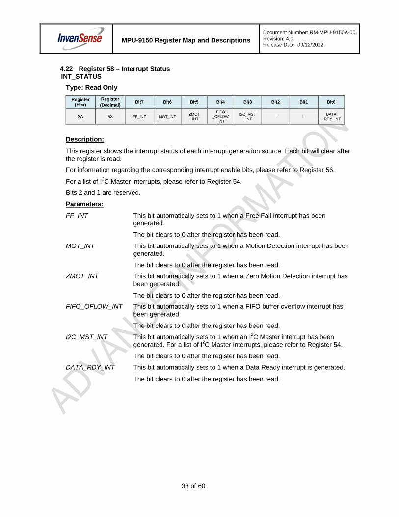
4.22 Register 58 – Interrupt Status INT_STATUS
Type: Read Only Register
(Hex) Register (Decimal) Bit7 Bit6 Bit5 Bit4 Bit3 Bit2 Bit1 Bit0
3A 58 FF_INT MOT_INT ZMOT _INT
FIFO _OFLOW
_INT
I2C_MST _INT - - DATA
_RDY_INT
This register shows the interrupt status of each interrupt generation source. Each bit will clear after the register is read.
Description:
For information regarding the corresponding interrupt enable bits, please refer to Register 56.
For a list of I2C Master interrupts, please refer to Register 54.
Bits 2 and 1 are reserved.
FF_INT This bit automatically sets to 1 when a Free Fall interrupt has been generated.
Parameters:
The bit clears to 0 after the register has been read.
MOT_INT This bit automatically sets to 1 when a Motion Detection interrupt has been generated.
The bit clears to 0 after the register has been read.
ZMOT_INT This bit automatically sets to 1 when a Zero Motion Detection interrupt has been generated.
The bit clears to 0 after the register has been read.
FIFO_OFLOW_INT This bit automatically sets to 1 when a FIFO buffer overflow interrupt has been generated.
The bit clears to 0 after the register has been read.
I2C_MST_INT This bit automatically sets to 1 when an I2C Master interrupt has been generated. For a list of I2C Master interrupts, please refer to Register 54.
The bit clears to 0 after the register has been read.
DATA_RDY_INT This bit automatically sets to 1 when a Data Ready interrupt is generated.
The bit clears to 0 after the register has been read.
MPU-9150 Register Map and Descriptions
Document Number: RM-MPU-9150A-00 Revision: 4.0 Release Date: 09/12/2012
34 of 60
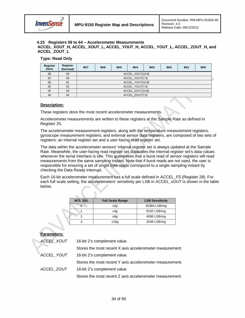
4.23 Registers 59 to 64 – Accelerometer Measurements ACCEL_XOUT_H, ACCEL_XOUT_L, ACCEL_YOUT_H, ACCEL_YOUT_L, ACCEL_ZOUT_H, and ACCEL_ZOUT_L
Type: Read Only Register
(Hex) Register (Decimal) Bit7 Bit6 Bit5 Bit4 Bit3 Bit2 Bit1 Bit0
3B 59 ACCEL_XOUT[15:8] 3C 60 ACCEL_XOUT[7:0] 3D 61 ACCEL_YOUT[15:8] 3E 62 ACCEL_YOUT[7:0] 3F 63 ACCEL_ZOUT[15:8] 40 64 ACCEL_ZOUT[7:0]
These registers store the most recent accelerometer measurements.
Description:
Accelerometer measurements are written to these registers at the Sample Rate as defined in Register 25.
The accelerometer measurement registers, along with the temperature measurement registers, gyroscope measurement registers, and external sensor data registers, are composed of two sets of registers: an internal register set and a user-facing read register set.
The data within the accelerometer sensors’ internal register set is always updated at the Sample Rate. Meanwhile, the user-facing read register set duplicates the internal register set’s data values whenever the serial interface is idle. This guarantees that a burst read of sensor registers will read measurements from the same sampling instant. Note that if burst reads are not used, the user is responsible for ensuring a set of single byte reads correspond to a single sampling instant by checking the Data Ready interrupt.
Each 16-bit accelerometer measurement has a full scale defined in ACCEL_FS (Register 28). For each full scale setting, the accelerometers’ sensitivity per LSB in ACCEL_xOUT is shown in the table below.
AFS_SEL Full Scale Range LSB Sensitivity 0 ±2g 16384 LSB/mg
1 ±4g 8192 LSB/mg
2 ±8g 4096 LSB/mg
3 ±16g 2048 LSB/mg
ACCEL_XOUT 16-bit 2’s complement value.
Parameters:
Stores the most recent X axis accelerometer measurement.
ACCEL_YOUT 16-bit 2’s complement value.
Stores the most recent Y axis accelerometer measurement.
ACCEL_ZOUT 16-bit 2’s complement value.
Stores the most recent Z axis accelerometer measurement.

MPU-9150 Register Map and Descriptions
Document Number: RM-MPU-9150A-00 Revision: 4.0 Release Date: 09/12/2012
35 of 60
4.24 Registers 65 and 66 – Temperature Measurement TEMP_OUT_H and TEMP_OUT_L
Type: Read Only Register
(Hex) Register (Decimal) Bit7 Bit6 Bit5 Bit4 Bit3 Bit2 Bit1 Bit0
41 65 TEMP_OUT[15:8] 42 66 TEMP_OUT[7:0]
These registers store the most recent temperature sensor measurement.
Description:
Temperature measurements are written to these registers at the Sample Rate as defined in Register 25.
These temperature measurement registers, along with the accelerometer measurement registers, gyroscope measurement registers, and external sensor data registers, are composed of two sets of registers: an internal register set and a user-facing read register set.
The data within the temperature sensor’s internal register set is always updated at the Sample Rate. Meanwhile, the user-facing read register set duplicates the internal register set’s data values whenever the serial interface is idle. This guarantees that a burst read of sensor registers will read measurements from the same sampling instant. Note that if burst reads are not used, the user is responsible for ensuring a set of single byte reads correspond to a single sampling instant by checking the Data Ready interrupt.
The scale factor and offset for the temperature sensor are found in the Electrical Specifications table in the MPU-9150 Product Specification document.
The temperature in degrees C for a given register value may be computed as:
Temperature in degrees C = (TEMP_OUT Register Value as a signed quantity)/340 + 35
Please note that the math in the above equation is in decimal.
TEMP_OUT 16-bit signed value.
Parameters:
Stores the most recent temperature sensor measurement.

MPU-9150 Register Map and Descriptions
Document Number: RM-MPU-9150A-00 Revision: 4.0 Release Date: 09/12/2012
36 of 60
4.25 Registers 67 to 72 – Gyroscope Measurements GYRO_XOUT_H, GYRO_XOUT_L, GYRO_YOUT_H, GYRO_YOUT_L, GYRO_ZOUT_H, and GYRO_ZOUT_L
Type: Read Only Register
(Hex) Register (Decimal) Bit7 Bit6 Bit5 Bit4 Bit3 Bit2 Bit1 Bit0
43 67 GYRO_XOUT[15:8] 44 68 GYRO_XOUT[7:0] 45 69 GYRO_YOUT[15:8] 46 70 GYRO_YOUT[7:0] 47 71 GYRO_ZOUT[15:8] 48 72 GYRO_ZOUT[7:0]
These registers store the most recent gyroscope measurements.
Description:
Gyroscope measurements are written to these registers at the Sample Rate as defined in Register 25.
These gyroscope measurement registers, along with the accelerometer measurement registers, temperature measurement registers, and external sensor data registers, are composed of two sets of registers: an internal register set and a user-facing read register set.
The data within the gyroscope sensors’ internal register set is always updated at the Sample Rate. Meanwhile, the user-facing read register set duplicates the internal register set’s data values whenever the serial interface is idle. This guarantees that a burst read of sensor registers will read measurements from the same sampling instant. Note that if burst reads are not used, the user is responsible for ensuring a set of single byte reads correspond to a single sampling instant by checking the Data Ready interrupt.
Each 16-bit gyroscope measurement has a full scale defined in FS_SEL (Register 27). For each full scale setting, the gyroscopes’ sensitivity per LSB in GYRO_xOUT is shown in the table below:
FS_SEL Full Scale Range LSB Sensitivity 0 ± 250 °/s 131 LSB/°/s 1 ± 500 °/s 65.5 LSB/°/s 2 ± 1000 °/s 32.8 LSB/°/s 3 ± 2000 °/s 16.4 LSB/°/s
GYRO_XOUT 16-bit 2’s complement value.
Parameters:
Stores the most recent X axis gyroscope measurement.
GYRO_YOUT 16-bit 2’s complement value.
Stores the most recent Y axis gyroscope measurement.
GYRO_ZOUT 16-bit 2’s complement value.
Stores the most recent Z axis gyroscope measurement.
MPU-9150 Register Map and Descriptions
Document Number: RM-MPU-9150A-00 Revision: 4.0 Release Date: 09/12/2012
37 of 60
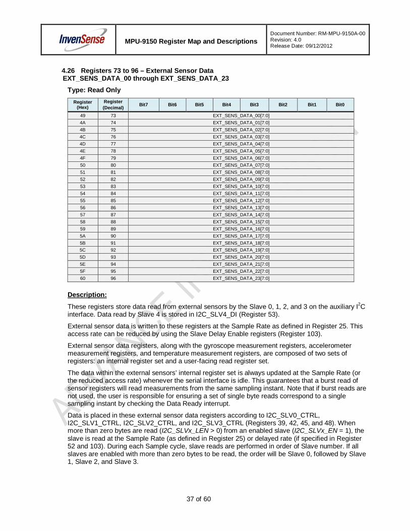
4.26 Registers 73 to 96 – External Sensor Data EXT_SENS_DATA_00 through EXT_SENS_DATA_23
Type: Read Only Register
(Hex) Register (Decimal) Bit7 Bit6 Bit5 Bit4 Bit3 Bit2 Bit1 Bit0
49 73 EXT_SENS_DATA_00[7:0] 4A 74 EXT_SENS_DATA_01[7:0] 4B 75 EXT_SENS_DATA_02[7:0] 4C 76 EXT_SENS_DATA_03[7:0] 4D 77 EXT_SENS_DATA_04[7:0] 4E 78 EXT_SENS_DATA_05[7:0] 4F 79 EXT_SENS_DATA_06[7:0] 50 80 EXT_SENS_DATA_07[7:0] 51 81 EXT_SENS_DATA_08[7:0] 52 82 EXT_SENS_DATA_09[7:0] 53 83 EXT_SENS_DATA_10[7:0] 54 84 EXT_SENS_DATA_11[7:0] 55 85 EXT_SENS_DATA_12[7:0] 56 86 EXT_SENS_DATA_13[7:0] 57 87 EXT_SENS_DATA_14[7:0] 58 88 EXT_SENS_DATA_15[7:0] 59 89 EXT_SENS_DATA_16[7:0] 5A 90 EXT_SENS_DATA_17[7:0] 5B 91 EXT_SENS_DATA_18[7:0] 5C 92 EXT_SENS_DATA_19[7:0] 5D 93 EXT_SENS_DATA_20[7:0] 5E 94 EXT_SENS_DATA_21[7:0] 5F 95 EXT_SENS_DATA_22[7:0] 60 96 EXT_SENS_DATA_23[7:0]
These registers store data read from external sensors by the Slave 0, 1, 2, and 3 on the auxiliary I2C interface. Data read by Slave 4 is stored in I2C_SLV4_DI (Register 53).
Description:
External sensor data is written to these registers at the Sample Rate as defined in Register 25. This access rate can be reduced by using the Slave Delay Enable registers (Register 103).
External sensor data registers, along with the gyroscope measurement registers, accelerometer measurement registers, and temperature measurement registers, are composed of two sets of registers: an internal register set and a user-facing read register set.
The data within the external sensors’ internal register set is always updated at the Sample Rate (or the reduced access rate) whenever the serial interface is idle. This guarantees that a burst read of sensor registers will read measurements from the same sampling instant. Note that if burst reads are not used, the user is responsible for ensuring a set of single byte reads correspond to a single sampling instant by checking the Data Ready interrupt.
Data is placed in these external sensor data registers according to I2C_SLV0_CTRL, I2C_SLV1_CTRL, I2C_SLV2_CTRL, and I2C_SLV3_CTRL (Registers 39, 42, 45, and 48). When more than zero bytes are read (I2C_SLVx_LEN > 0) from an enabled slave (I2C_SLVx_EN = 1), the slave is read at the Sample Rate (as defined in Register 25) or delayed rate (if specified in Register 52 and 103). During each Sample cycle, slave reads are performed in order of Slave number. If all slaves are enabled with more than zero bytes to be read, the order will be Slave 0, followed by Slave 1, Slave 2, and Slave 3.

MPU-9150 Register Map and Descriptions
Document Number: RM-MPU-9150A-00 Revision: 4.0 Release Date: 09/12/2012
38 of 60
Each enabled slave will have EXT_SENS_DATA registers associated with it by number of bytes read (I2C_SLVx_LEN) in order of slave number, starting from EXT_SENS_DATA_00. Note that this means enabling or disabling a slave may change the higher numbered slaves’ associated registers. Furthermore, if fewer total bytes are being read from the external sensors as a result of such a change, then the data remaining in the registers which no longer have an associated slave device (i.e. high numbered registers) will remain in these previously allocated registers unless reset.
If the sum of the read lengths of all SLVx transactions exceed the number of available EXT_SENS_DATA registers , the excess bytes will be dropped. There are 24 EXT_SENS_DATA registers and hence the total read lengths between all the slaves cannot be greater than 24 or some bytes will be lost.
Note
: Slave 4’s behavior is distinct from that of Slaves 0-3. For further information regarding the characteristics of Slave 4, please refer to Registers 49 to 53.
Suppose that Slave 0 is enabled with 4 bytes to be read (I2C_SLV0_EN = 1 and I2C_SLV0_LEN = 4) while Slave 1 is enabled with 2 bytes to be read, (I2C_SLV1_EN=1 and I2C_SLV1_LEN = 2). In such a situation, EXT_SENS_DATA _00 through _03 will be associated with Slave 0, while EXT_SENS_DATA _04 and 05 will be associated with Slave 1.
Example:
If Slave 2 is enabled as well, registers starting from EXT_SENS_DATA_06 will be allocated to Slave 2.
If Slave 2 is disabled while Slave 3 is enabled in this same situation, then registers starting from EXT_SENS_DATA_06 will be allocated to Slave 3 instead.
If a slave is disabled at any time, the space initially allocated to the slave in the EXT_SENS_DATA register, will remain associated with that slave. This is to avoid dynamic adjustment of the register allocation.
Register Allocation for Dynamic Disable vs. Normal Disable
The allocation of the EXT_SENS_DATA registers is recomputed only when (1) all slaves are disabled, or (2) the I2C_MST_RST bit is set (Register 106) .
This above is also true if one of the slaves gets NACKed and stops functioning.
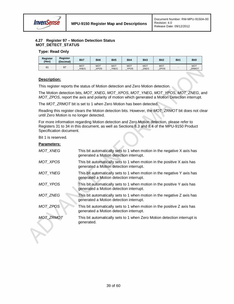
MPU-9150 Register Map and Descriptions
Document Number: RM-MPU-9150A-00 Revision: 4.0 Release Date: 09/12/2012
39 of 60
4.27 Register 97 – Motion Detection Status MOT_DETECT_STATUS
Type: Read Only Register
(Hex) Register (Decimal) Bit7 Bit6 Bit5 Bit4 Bit3 Bit2 Bit1 Bit0
61 97 MOT _XNEG
MOT _XPOS
MOT _YNEG
MOT _YPOS
MOT _ZNEG
MOT _ZPOS - MOT
_ZRMOT
This register reports the status of Motion detection and Zero Motion detection.
Description:
The Motion detection bits, MOT_XNEG, MOT_XPOS, MOT_YNEG, MOT_YPOS, MOT_ZNEG, and MOT_ZPOS, report the axis and polarity of motion which generated a Motion Detection interrupt.
The MOT_ZRMOT bit is set to 1 when Zero Motion has been detected.
Reading this register clears the Motion detection bits. However, the MOT_ZRMOT bit does not clear until Zero Motion is no longer detected.
For more information regarding Motion detection and Zero Motion detection, please refer to Registers 31 to 34 in this document, as well as Sections 8.3 and 8.4 of the MPU-9150 Product Specification document.
Bit 1 is reserved.
MOT_XNEG This bit automatically sets to 1 when motion in the negative X axis has generated a Motion detection interrupt.
Parameters:
MOT_XPOS This bit automatically sets to 1 when motion in the positive X axis has generated a Motion detection interrupt.
MOT_YNEG This bit automatically sets to 1 when motion in the negative Y axis has generated a Motion detection interrupt.
MOT_YPOS This bit automatically sets to 1 when motion in the positive Y axis has generated a Motion detection interrupt.
MOT_ZNEG This bit automatically sets to 1 when motion in the negative Z axis has generated a Motion detection interrupt.
MOT_ZPOS This bit automatically sets to 1 when motion in the positive Z axis has generated a Motion detection interrupt.
MOT_ZRMOT This bit automatically sets to 1 when Zero Motion detection interrupt is generated.

MPU-9150 Register Map and Descriptions
Document Number: RM-MPU-9150A-00 Revision: 4.0 Release Date: 09/12/2012
40 of 60
4.28 Register 99 – I2C Slave 0 Data Out I2C_SLV0_DO
Type: Read/Write Register
(Hex) Register (Decimal) Bit7 Bit6 Bit5 Bit4 Bit3 Bit2 Bit1 Bit0
63 99 I2C_SLV0_DO[7:0]
This register holds the output data written into Slave 0 when Slave 0 is set to write mode.
Description:
For further information regarding Slave 0 control, please refer to Registers 37 to 39.
I2C_SLV0_DO 8 bit unsigned value that is written into Slave 0 when Slave 0 is set to write mode.
Parameters:
4.29 Register 100 – I2C Slave 1 Data Out I2C_SLV1_DO
Type: Read/Write Register
(Hex) Register (Decimal) Bit7 Bit6 Bit5 Bit4 Bit3 Bit2 Bit1 Bit0
64 100 I2C_SLV1_DO[7:0]
This register holds the output data written into Slave 1 when Slave 1 is set to write mode.
Description:
For further information regarding Slave 1 control, please refer to Registers 40 to 42.
I2C_SLV1_DO 8 bit unsigned value that is written into Slave 1 when Slave 1 is set to write mode.
Parameters:

MPU-9150 Register Map and Descriptions
Document Number: RM-MPU-9150A-00 Revision: 4.0 Release Date: 09/12/2012
41 of 60
4.30 Register 101 – I2C Slave 2 Data Out I2C_SLV2_DO
Type: Read/Write Register
(Hex) Register (Decimal) Bit7 Bit6 Bit5 Bit4 Bit3 Bit2 Bit1 Bit0
65 101 I2C_SLV2_DO[7:0]
This register holds the output data written into Slave 2 when Slave 2 is set to write mode.
Description:
For further information regarding Slave 2 control, please refer to Registers 43 to 45.
I2C_SLV2_DO 8 bit unsigned value that is written into Slave 2 when Slave 2 is set to write mode.
Parameters:
4.31 Register 102 – I2C Slave 3 Data Out
I2C_SLV3_DO
Type: Read/Write Register
(Hex) Register (Decimal) Bit7 Bit6 Bit5 Bit4 Bit3 Bit2 Bit1 Bit0
66 102 I2C_SLV3_DO[7:0]
This register holds the output data written into Slave 3 when Slave 3 is set to write mode.
Description:
For further information regarding Slave 3 control, please refer to Registers 46 to 48.
I2C_SLV3_DO 8 bit unsigned value that is written into Slave 3 when Slave 3 is set to write mode.
Parameters:

MPU-9150 Register Map and Descriptions
Document Number: RM-MPU-9150A-00 Revision: 4.0 Release Date: 09/12/2012
42 of 60
4.32 Register 103 – I2C Master Delay Control I2C_MST_DELAY_CTRL
Type: Read/Write Register
(Hex) Register (Decimal) Bit7 Bit6 Bit5 Bit4 Bit3 Bit2 Bit1 Bit0
67 103 DELAY
_ES _SHADOW
- - I2C_SLV4 _DLY_EN
I2C_SLV3 _DLY_EN
I2C_SLV2 _DLY_EN
I2C_SLV1 _DLY_EN
I2C_SLV0 _DLY_EN
This register is used to specify the timing of external sensor data shadowing. The register is also used to decrease the access rate of slave devices relative to the Sample Rate.
Description:
When DELAY_ES_SHADOW is set to 1, shadowing of external sensor data is delayed until all data has been received.
When I2C_SLV4_DLY_EN, I2C_SLV3_DLY_EN, I2C_SLV2_DLY_EN, I2C_SLV1_DLY_EN, and I2C_SLV0_DLY_EN are enabled, the rate of access for the corresponding slave devices is reduced.
When a slave’s access rate is decreased relative to the Sample Rate, the slave is accessed every
1 / (1 + I2C_MST_DLY) samples.
This base Sample Rate in turn is determined by SMPLRT_DIV (register 25) and DLPF_CFG (register 26).
For further information regarding I2C_MST_DLY, please refer to register 52.
For further information regarding the Sample Rate, please refer to register 25.
Bits 6 and 5 are reserved.
DELAY_ES_SHADOW When set, delays shadowing of external sensor data until all data has been received.
Parameters:
I2C_SLV4_DLY_EN When enabled, slave 4 will only be accessed at a decreased rate.
I2C_SLV3_DLY_EN When enabled, slave 3 will only be accessed at a decreased rate.
I2C_SLV2_DLY_EN When enabled, slave 2 will only be accessed at a decreased rate.
I2C_SLV1_DLY_EN When enabled, slave 1 will only be accessed at a decreased rate.
I2C_SLV0_DLY_EN When enabled, slave 0 will only be accessed at a decreased rate.

MPU-9150 Register Map and Descriptions
Document Number: RM-MPU-9150A-00 Revision: 4.0 Release Date: 09/12/2012
43 of 60
4.33 Register 104 – Signal Path Reset SIGNAL_PATH_RESET
Type: Write Only Register
(Hex) Register (Decimal) Bit7 Bit6 Bit5 Bit4 Bit3 Bit2 Bit1 Bit0
68 104 - - - - - GYRO _RESET
ACCEL _RESET
TEMP _RESET
This register is used to reset the analog and digital signal paths of the gyroscope, accelerometer, and temperature sensors.
Description:
The reset will revert the signal path analog to digital converters and filters to their power up configurations.
Note:
Bits 7 through 3 are reserved.
This register does not clear the sensor registers.
GYRO_RESET When set to 1, this bit resets the gyroscope analog and digital signal paths.
Parameters:
ACCEL_RESET When set to 1, this bit resets the accelerometer analog and digital signal paths.
TEMP_RESET When set to 1, this bit resets the temperature sensor analog and digital signal paths.
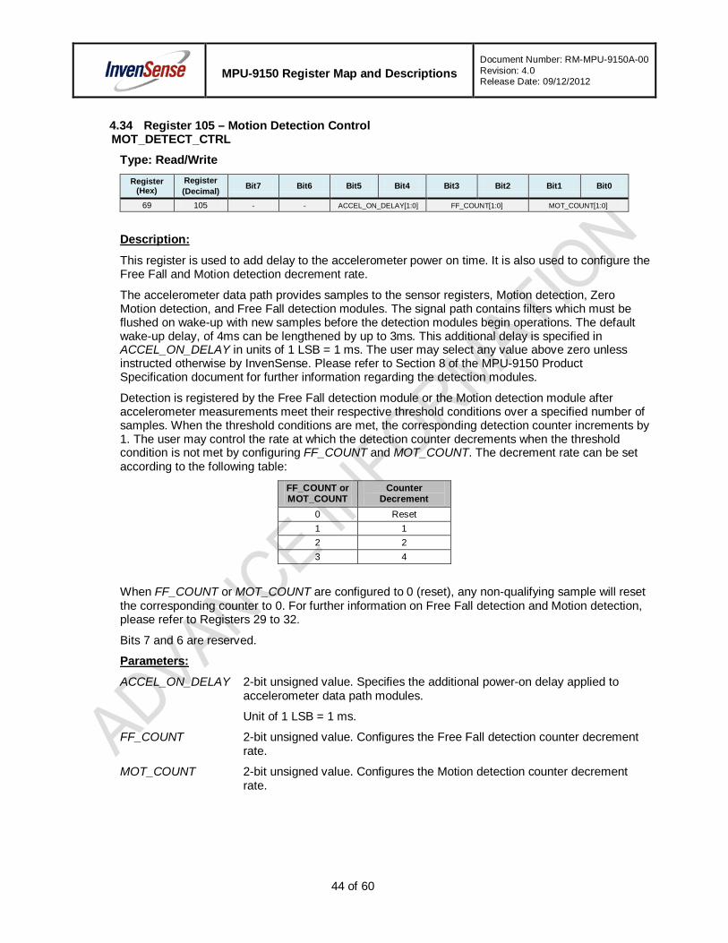
MPU-9150 Register Map and Descriptions
Document Number: RM-MPU-9150A-00 Revision: 4.0 Release Date: 09/12/2012
44 of 60
4.34 Register 105 – Motion Detection Control MOT_DETECT_CTRL
Type: Read/Write Register
(Hex) Register (Decimal) Bit7 Bit6 Bit5 Bit4 Bit3 Bit2 Bit1 Bit0
69 105 - - ACCEL_ON_DELAY[1:0] FF_COUNT[1:0] MOT_COUNT[1:0]
This register is used to add delay to the accelerometer power on time. It is also used to configure the Free Fall and Motion detection decrement rate.
Description:
The accelerometer data path provides samples to the sensor registers, Motion detection, Zero Motion detection, and Free Fall detection modules. The signal path contains filters which must be flushed on wake-up with new samples before the detection modules begin operations. The default wake-up delay, of 4ms can be lengthened by up to 3ms. This additional delay is specified in ACCEL_ON_DELAY in units of 1 LSB = 1 ms. The user may select any value above zero unless instructed otherwise by InvenSense. Please refer to Section 8 of the MPU-9150 Product Specification document for further information regarding the detection modules.
Detection is registered by the Free Fall detection module or the Motion detection module after accelerometer measurements meet their respective threshold conditions over a specified number of samples. When the threshold conditions are met, the corresponding detection counter increments by 1. The user may control the rate at which the detection counter decrements when the threshold condition is not met by configuring FF_COUNT and MOT_COUNT. The decrement rate can be set according to the following table:
FF_COUNT or MOT_COUNT
Counter Decrement
0 Reset 1 1 2 2 3 4
When FF_COUNT or MOT_COUNT are configured to 0 (reset), any non-qualifying sample will reset the corresponding counter to 0. For further information on Free Fall detection and Motion detection, please refer to Registers 29 to 32.
Bits 7 and 6 are reserved.
ACCEL_ON_DELAY 2-bit unsigned value. Specifies the additional power-on delay applied to accelerometer data path modules.
Parameters:
Unit of 1 LSB = 1 ms.
FF_COUNT 2-bit unsigned value. Configures the Free Fall detection counter decrement rate.
MOT_COUNT 2-bit unsigned value. Configures the Motion detection counter decrement rate.
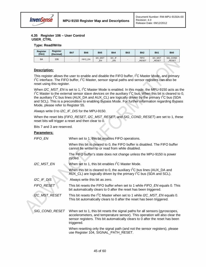
MPU-9150 Register Map and Descriptions
Document Number: RM-MPU-9150A-00 Revision: 4.0 Release Date: 09/12/2012
45 of 60
4.35 Register 106 – User Control USER_CTRL
Type: Read/Write Register
(Hex) Register (Decimal) Bit7 Bit6 Bit5 Bit4 Bit3 Bit2 Bit1 Bit0
6A 106 - FIFO_EN I2C_MST
_EN I2C_IF _DIS -
FIFO _RESET
I2C_MST _RESET
SIG_COND _RESET
This register allows the user to enable and disable the FIFO buffer, I2C Master Mode, and primary I2C interface. The FIFO buffer, I2C Master, sensor signal paths and sensor registers can also be reset using this register.
Description:
When I2C_MST_EN is set to 1, I2C Master Mode is enabled. In this mode, the MPU-9150 acts as the I2C Master to the external sensor slave devices on the auxiliary I2C bus. When this bit is cleared to 0, the auxiliary I2C bus lines (AUX_DA and AUX_CL) are logically driven by the primary I2C bus (SDA and SCL). This is a precondition to enabling Bypass Mode. For further information regarding Bypass Mode, please refer to Register 55.
Always write 0 to I2C_IF_DIS for the MPU-9150.
When the reset bits (FIFO_RESET, I2C_MST_RESET, and SIG_COND_RESET) are set to 1, these reset bits will trigger a reset and then clear to 0.
Bits 7 and 3 are reserved.
FIFO_EN When set to 1, this bit enables FIFO operations.
Parameters:
When this bit is cleared to 0, the FIFO buffer is disabled. The FIFO buffer cannot be written to or read from while disabled.
The FIFO buffer’s state does not change unless the MPU-9150 is power cycled.
I2C_MST_EN When set to 1, this bit enables I2C Master Mode.
When this bit is cleared to 0, the auxiliary I2C bus lines (AUX_DA and AUX_CL) are logically driven by the primary I2C bus (SDA and SCL).
I2C_IF_DIS Always write this bit as zero.
FIFO_RESET This bit resets the FIFO buffer when set to 1 while FIFO_EN equals 0. This bit automatically clears to 0 after the reset has been triggered.
I2C_MST_RESET This bit resets the I2C Master when set to 1 while I2C_MST_EN equals 0. This bit automatically clears to 0 after the reset has been triggered.
SIG_COND_RESET When set to 1, this bit resets the signal paths for all sensors (gyroscopes, accelerometers, and temperature sensor). This operation will also clear the sensor registers. This bit automatically clears to 0 after the reset has been triggered.
When resetting only the signal path (and not the sensor registers), please use Register 104, SIGNAL_PATH_RESET.
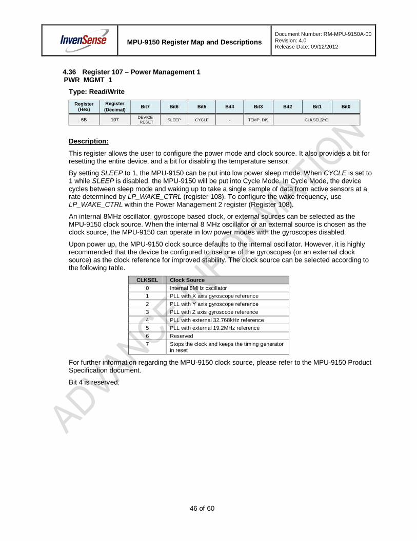
MPU-9150 Register Map and Descriptions
Document Number: RM-MPU-9150A-00 Revision: 4.0 Release Date: 09/12/2012
46 of 60
4.36 Register 107 – Power Management 1 PWR_MGMT_1
Type: Read/Write Register
(Hex) Register (Decimal) Bit7 Bit6 Bit5 Bit4 Bit3 Bit2 Bit1 Bit0
6B 107 DEVICE _RESET SLEEP CYCLE - TEMP_DIS CLKSEL[2:0]
This register allows the user to configure the power mode and clock source. It also provides a bit for resetting the entire device, and a bit for disabling the temperature sensor.
Description:
By setting SLEEP to 1, the MPU-9150 can be put into low power sleep mode. When CYCLE is set to 1 while SLEEP is disabled, the MPU-9150 will be put into Cycle Mode. In Cycle Mode, the device cycles between sleep mode and waking up to take a single sample of data from active sensors at a rate determined by LP_WAKE_CTRL (register 108). To configure the wake frequency, use LP_WAKE_CTRL within the Power Management 2 register (Register 108).
An internal 8MHz oscillator, gyroscope based clock, or external sources can be selected as the MPU-9150 clock source. When the internal 8 MHz oscillator or an external source is chosen as the clock source, the MPU-9150 can operate in low power modes with the gyroscopes disabled.
Upon power up, the MPU-9150 clock source defaults to the internal oscillator. However, it is highly recommended that the device be configured to use one of the gyroscopes (or an external clock source) as the clock reference for improved stability. The clock source can be selected according to the following table.
CLKSEL Clock Source 0 Internal 8MHz oscillator 1 PLL with X axis gyroscope reference 2 PLL with Y axis gyroscope reference 3 PLL with Z axis gyroscope reference 4 PLL with external 32.768kHz reference 5 PLL with external 19.2MHz reference 6 Reserved 7 Stops the clock and keeps the timing generator
in reset
For further information regarding the MPU-9150 clock source, please refer to the MPU-9150 Product Specification document.
Bit 4 is reserved.

MPU-9150 Register Map and Descriptions
Document Number: RM-MPU-9150A-00 Revision: 4.0 Release Date: 09/12/2012
47 of 60
DEVICE_RESET When set to 1, this bit resets all internal registers to their default values.
Parameters:
The bit automatically clears to 0 once the reset is done.
The default values for each register can be found in Section 3.
SLEEP When set to 1, this bit puts the MPU-9150 into sleep mode.
CYCLE When this bit is set to 1 and SLEEP is disabled, the MPU-9150 will cycle between sleep mode and waking up to take a single sample of data from active sensors at a rate determined by LP_WAKE_CTRL (register 108).
TEMP_DIS When set to 1, this bit disables the temperature sensor.
CLKSEL 3-bit unsigned value. Specifies the clock source of the device.
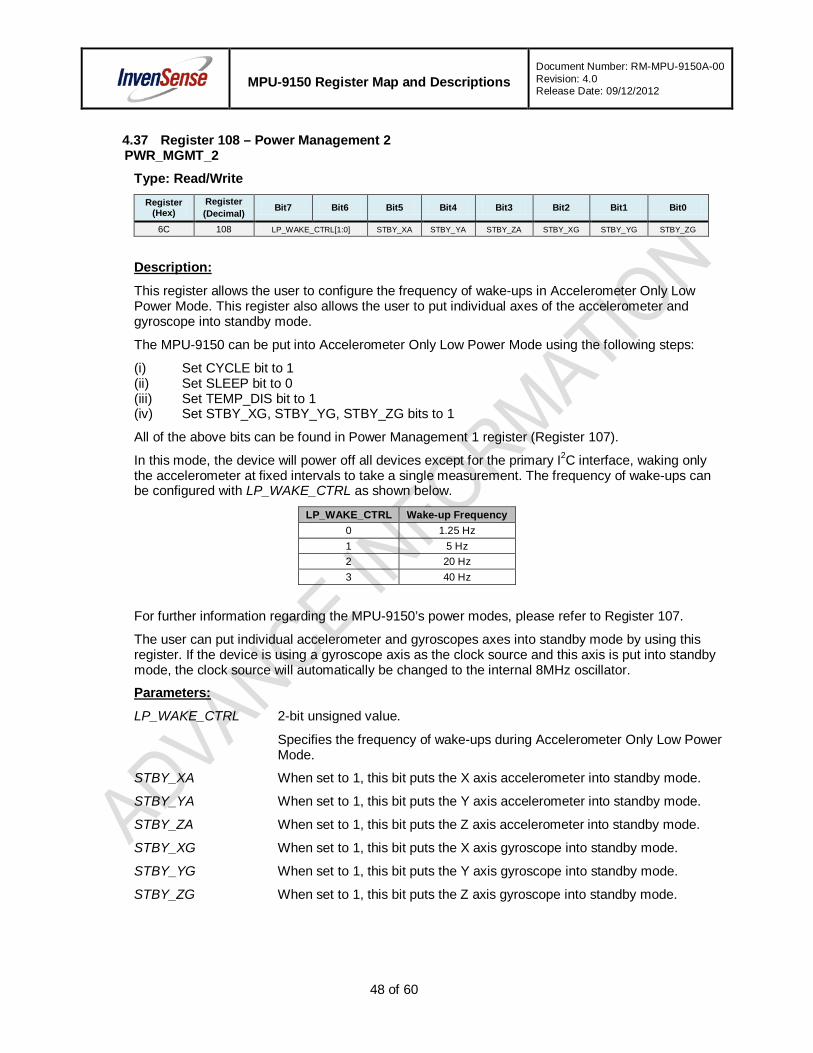
MPU-9150 Register Map and Descriptions
Document Number: RM-MPU-9150A-00 Revision: 4.0 Release Date: 09/12/2012
48 of 60
4.37 Register 108 – Power Management 2 PWR_MGMT_2
Type: Read/Write Register
(Hex) Register (Decimal) Bit7 Bit6 Bit5 Bit4 Bit3 Bit2 Bit1 Bit0
6C 108 LP_WAKE_CTRL[1:0] STBY_XA STBY_YA STBY_ZA STBY_XG STBY_YG STBY_ZG
This register allows the user to configure the frequency of wake-ups in Accelerometer Only Low Power Mode. This register also allows the user to put individual axes of the accelerometer and gyroscope into standby mode.
Description:
The MPU-9150 can be put into Accelerometer Only Low Power Mode using the following steps:
(i) Set CYCLE bit to 1 (ii) Set SLEEP bit to 0 (iii) Set TEMP_DIS bit to 1 (iv) Set STBY_XG, STBY_YG, STBY_ZG bits to 1
All of the above bits can be found in Power Management 1 register (Register 107).
In this mode, the device will power off all devices except for the primary I2C interface, waking only the accelerometer at fixed intervals to take a single measurement. The frequency of wake-ups can be configured with LP_WAKE_CTRL as shown below.
LP_WAKE_CTRL Wake-up Frequency 0 1.25 Hz 1 5 Hz 2 20 Hz 3 40 Hz
For further information regarding the MPU-9150’s power modes, please refer to Register 107.
The user can put individual accelerometer and gyroscopes axes into standby mode by using this register. If the device is using a gyroscope axis as the clock source and this axis is put into standby mode, the clock source will automatically be changed to the internal 8MHz oscillator.
LP_WAKE_CTRL 2-bit unsigned value.
Parameters:
Specifies the frequency of wake-ups during Accelerometer Only Low Power Mode.
STBY_XA When set to 1, this bit puts the X axis accelerometer into standby mode.
STBY_YA When set to 1, this bit puts the Y axis accelerometer into standby mode.
STBY_ZA When set to 1, this bit puts the Z axis accelerometer into standby mode.
STBY_XG When set to 1, this bit puts the X axis gyroscope into standby mode.
STBY_YG When set to 1, this bit puts the Y axis gyroscope into standby mode.
STBY_ZG When set to 1, this bit puts the Z axis gyroscope into standby mode.

MPU-9150 Register Map and Descriptions
Document Number: RM-MPU-9150A-00 Revision: 4.0 Release Date: 09/12/2012
49 of 60
4.38 Register 114 and 115 – FIFO Count Registers FIFO_COUNT_H and FIFO_COUNT_L
Type: Read Only Register
(Hex) Register (Decimal) Bit7 Bit6 Bit5 Bit4 Bit3 Bit2 Bit1 Bit0
72 114 - - - - - FIFO_COUNT[10:8] 73 115 FIFO_COUNT[7:0]
These registers keep track of the number of samples currently in the FIFO buffer.
Description:
These registers shadow the FIFO Count value. Both registers are loaded with the current sample count when FIFO_COUNT_H (Register 72) is read.
Note: Reading only FIFO_COUNT_L will not update the registers to the current sample count. FIFO_COUNT_H must be accessed first to update the contents of both these registers.
FIFO_COUNT should always be read in high-low order in order to guarantee that the most current FIFO Count value is read.
FIFO_COUNT 16-bit unsigned value. Indicates the number of bytes stored in the FIFO buffer. This number is in turn the number of bytes that can be read from the FIFO buffer and it is directly proportional to the number of samples available given the set of sensor data bound to be stored in the FIFO (register 35 and 36).
Parameters:
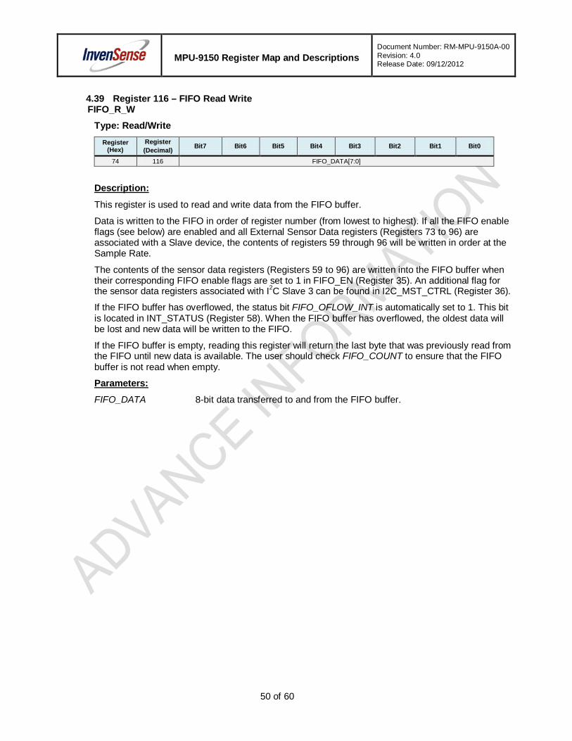
MPU-9150 Register Map and Descriptions
Document Number: RM-MPU-9150A-00 Revision: 4.0 Release Date: 09/12/2012
50 of 60
4.39 Register 116 – FIFO Read Write FIFO_R_W
Type: Read/Write Register
(Hex) Register (Decimal) Bit7 Bit6 Bit5 Bit4 Bit3 Bit2 Bit1 Bit0
74 116 FIFO_DATA[7:0]
This register is used to read and write data from the FIFO buffer.
Description:
Data is written to the FIFO in order of register number (from lowest to highest). If all the FIFO enable flags (see below) are enabled and all External Sensor Data registers (Registers 73 to 96) are associated with a Slave device, the contents of registers 59 through 96 will be written in order at the Sample Rate.
The contents of the sensor data registers (Registers 59 to 96) are written into the FIFO buffer when their corresponding FIFO enable flags are set to 1 in FIFO_EN (Register 35). An additional flag for the sensor data registers associated with I2C Slave 3 can be found in I2C_MST_CTRL (Register 36).
If the FIFO buffer has overflowed, the status bit FIFO_OFLOW_INT is automatically set to 1. This bit is located in INT_STATUS (Register 58). When the FIFO buffer has overflowed, the oldest data will be lost and new data will be written to the FIFO.
If the FIFO buffer is empty, reading this register will return the last byte that was previously read from the FIFO until new data is available. The user should check FIFO_COUNT to ensure that the FIFO buffer is not read when empty.
FIFO_DATA 8-bit data transferred to and from the FIFO buffer.
Parameters:

MPU-9150 Register Map and Descriptions
Document Number: RM-MPU-9150A-00 Revision: 4.0 Release Date: 09/12/2012
51 of 60
4.40 Register 117 – Who Am I WHO_AM_I
Type: Read Only Register
(Hex) Register (Decimal) Bit7 Bit6 Bit5 Bit4 Bit3 Bit2 Bit1 Bit0
75 117 - WHO_AM_I[6:1] -
This register is used to verify the identity of the device. The contents of WHO_AM_I are the upper 6 bits of the MPU-9150’s 7-bit I2C address. The least significant bit of the MPU-1950’s I2C address is determined by the value of the AD0 pin. The value of the AD0 pin is not reflected in this register.
Description:
The default value of the register is 0x68.
Bits 0 and 7 are reserved. (Hard coded to 0)
WHO_AM_I Contains the 6-bit I2C address of the MPU-9150.
Parameters:
The Power-On-Reset value of Bit6:Bit1 is 110 100.
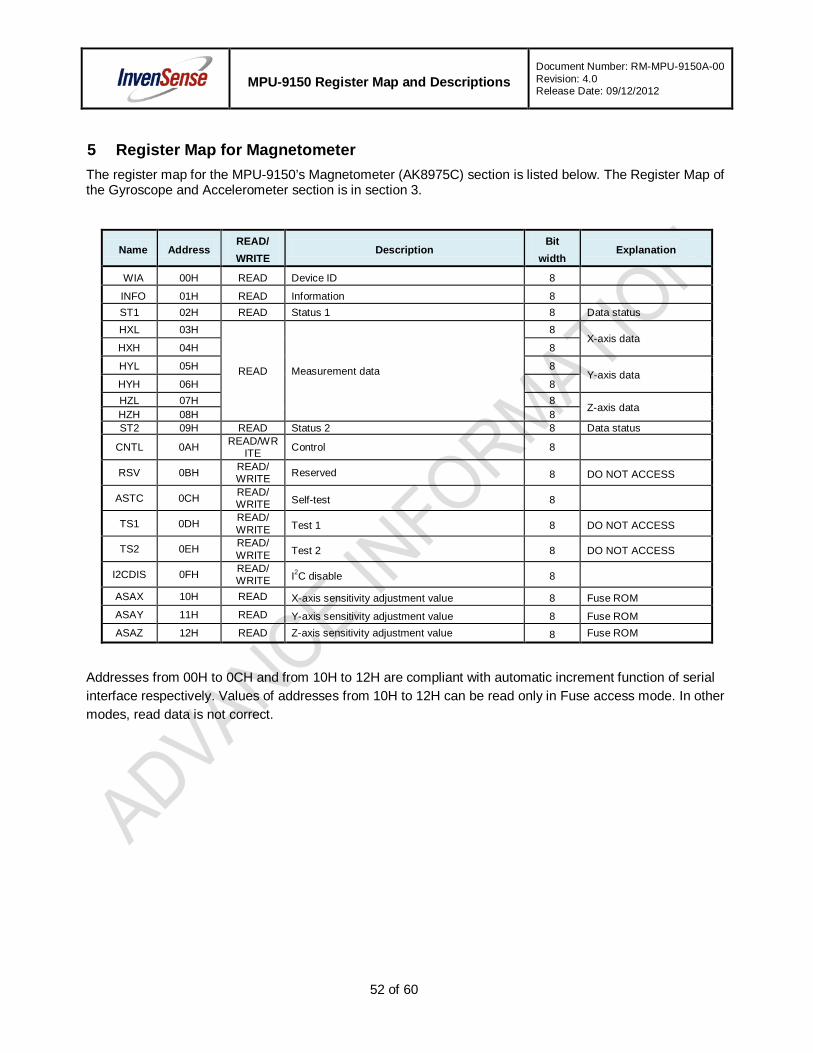
MPU-9150 Register Map and Descriptions
Document Number: RM-MPU-9150A-00 Revision: 4.0 Release Date: 09/12/2012
52 of 60
5 Register Map for Magnetometer The register map for the MPU-9150’s Magnetometer (AK8975C) section is listed below. The Register Map of the Gyroscope and Accelerometer section is in section 3.
Name Address READ/ WRITE
Description Bit
width Explanation
WIA 00H READ Device ID 8
INFO 01H READ Information 8 ST1 02H READ Status 1 8 Data status HXL 03H
READ Measurement data
8 X-axis data
HXH 04H 8
HYL 05H 8 Y-axis data
HYH 06H 8 HZL 07H 8
Z-axis data HZH 08H 8 ST2 09H READ Status 2 8 Data status
CNTL 0AH READ/WRITE Control 8
RSV 0BH READ/ WRITE Reserved 8 DO NOT ACCESS
ASTC 0CH READ/ WRITE Self-test 8
TS1 0DH READ/ WRITE Test 1 8 DO NOT ACCESS
TS2 0EH READ/ WRITE Test 2 8 DO NOT ACCESS
I2CDIS 0FH READ/ WRITE I2C disable 8
ASAX 10H READ X-axis sensitivity adjustment value 8 Fuse ROM ASAY 11H READ Y-axis sensitivity adjustment value 8 Fuse ROM ASAZ 12H READ Z-axis sensitivity adjustment value 8 Fuse ROM
Addresses from 00H to 0CH and from 10H to 12H are compliant with automatic increment function of serial interface respectively. Values of addresses from 10H to 12H can be read only in Fuse access mode. In other modes, read data is not correct.
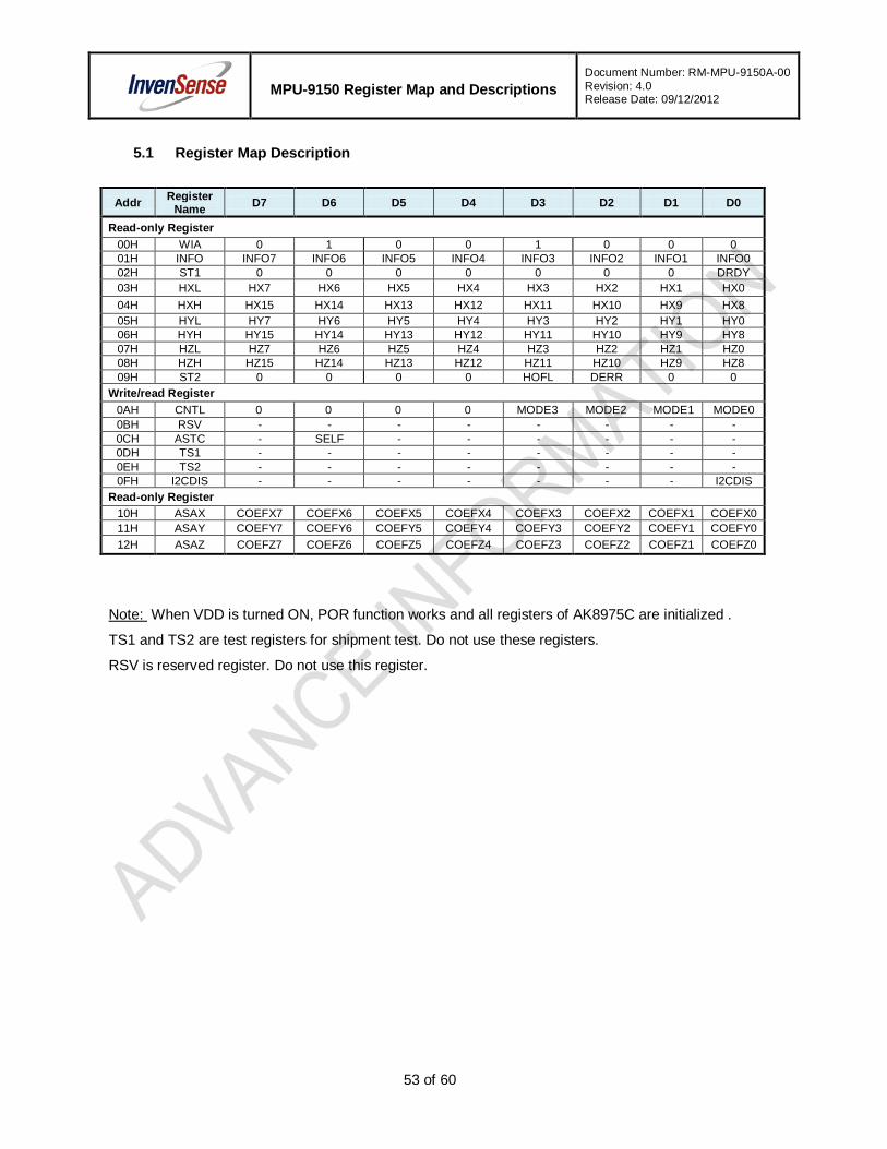
MPU-9150 Register Map and Descriptions
Document Number: RM-MPU-9150A-00 Revision: 4.0 Release Date: 09/12/2012
53 of 60
5.1 Register Map Description
Addr Register
Name D7 D6 D5 D4 D3 D2 D1 D0
Read-only Register 00H WIA 0 1 0 0 1 0 0 0 01H INFO INFO7 INFO6 INFO5 INFO4 INFO3 INFO2 INFO1 INFO0 02H ST1 0 0 0 0 0 0 0 DRDY 03H HXL HX7 HX6 HX5 HX4 HX3 HX2 HX1 HX0 04H HXH HX15 HX14 HX13 HX12 HX11 HX10 HX9 HX8 05H HYL HY7 HY6 HY5 HY4 HY3 HY2 HY1 HY0 06H HYH HY15 HY14 HY13 HY12 HY11 HY10 HY9 HY8 07H HZL HZ7 HZ6 HZ5 HZ4 HZ3 HZ2 HZ1 HZ0 08H HZH HZ15 HZ14 HZ13 HZ12 HZ11 HZ10 HZ9 HZ8 09H ST2 0 0 0 0 HOFL DERR 0 0
Write/read Register 0AH CNTL 0 0 0 0 MODE3 MODE2 MODE1 MODE0 0BH RSV - - - - - - - - 0CH ASTC - SELF - - - - - - 0DH TS1 - - - - - - - - 0EH TS2 - - - - - - - - 0FH I2CDIS - - - - - - - I2CDIS
Read-only Register 10H ASAX COEFX7 COEFX6 COEFX5 COEFX4 COEFX3 COEFX2 COEFX1 COEFX0 11H ASAY COEFY7 COEFY6 COEFY5 COEFY4 COEFY3 COEFY2 COEFY1 COEFY0 12H ASAZ COEFZ7 COEFZ6 COEFZ5 COEFZ4 COEFZ3 COEFZ2 COEFZ1 COEFZ0
Note:
TS1 and TS2 are test registers for shipment test. Do not use these registers.
When VDD is turned ON, POR function works and all registers of AK8975C are initialized .
RSV is reserved register. Do not use this register.

MPU-9150 Register Map and Descriptions
Document Number: RM-MPU-9150A-00 Revision: 4.0 Release Date: 09/12/2012
54 of 60
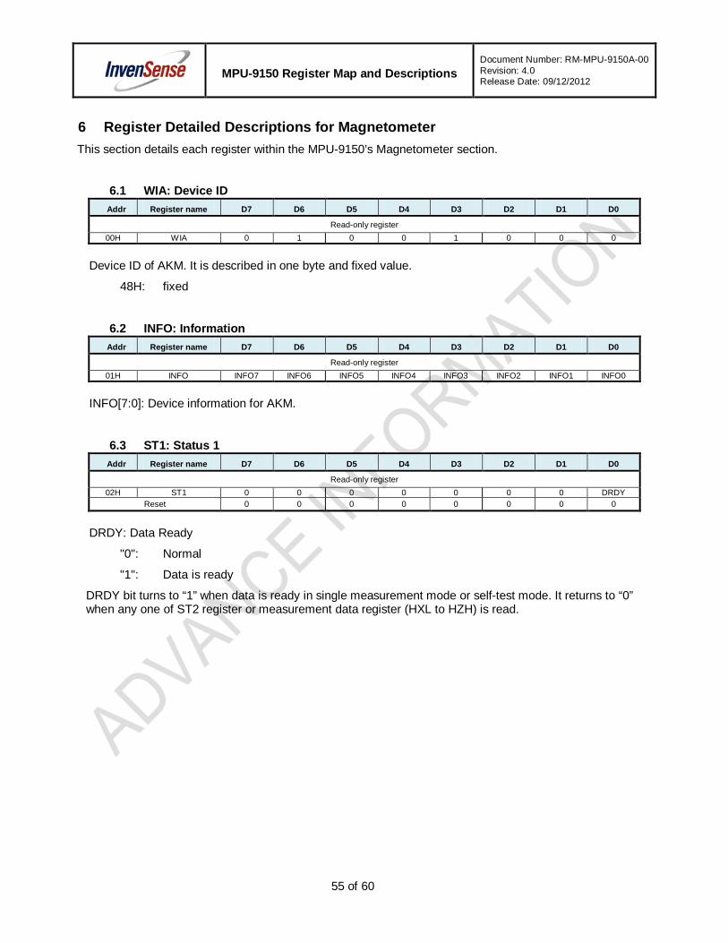
MPU-9150 Register Map and Descriptions
Document Number: RM-MPU-9150A-00 Revision: 4.0 Release Date: 09/12/2012
55 of 60
6 Register Detailed Descriptions for Magnetometer This section details each register within the MPU-9150’s Magnetometer section.
6.1 WIA: Device ID Addr Register name D7 D6 D5 D4 D3 D2 D1 D0
Read-only register 00H WIA 0 1 0 0 1 0 0 0
Device ID of AKM. It is described in one byte and fixed value.
48H: fixed
6.2 INFO: Information Addr Register name D7 D6 D5 D4 D3 D2 D1 D0
Read-only register 01H INFO INFO7 INFO6 INFO5 INFO4 INFO3 INFO2 INFO1 INFO0
INFO[7:0]: Device information for AKM.
6.3 ST1: Status 1 Addr Register name D7 D6 D5 D4 D3 D2 D1 D0
Read-only register 02H ST1 0 0 0 0 0 0 0 DRDY
Reset 0 0 0 0 0 0 0 0
DRDY: Data Ready
"0": Normal
"1": Data is ready
DRDY bit turns to “1” when data is ready in single measurement mode or self-test mode. It returns to “0” when any one of ST2 register or measurement data register (HXL to HZH) is read.
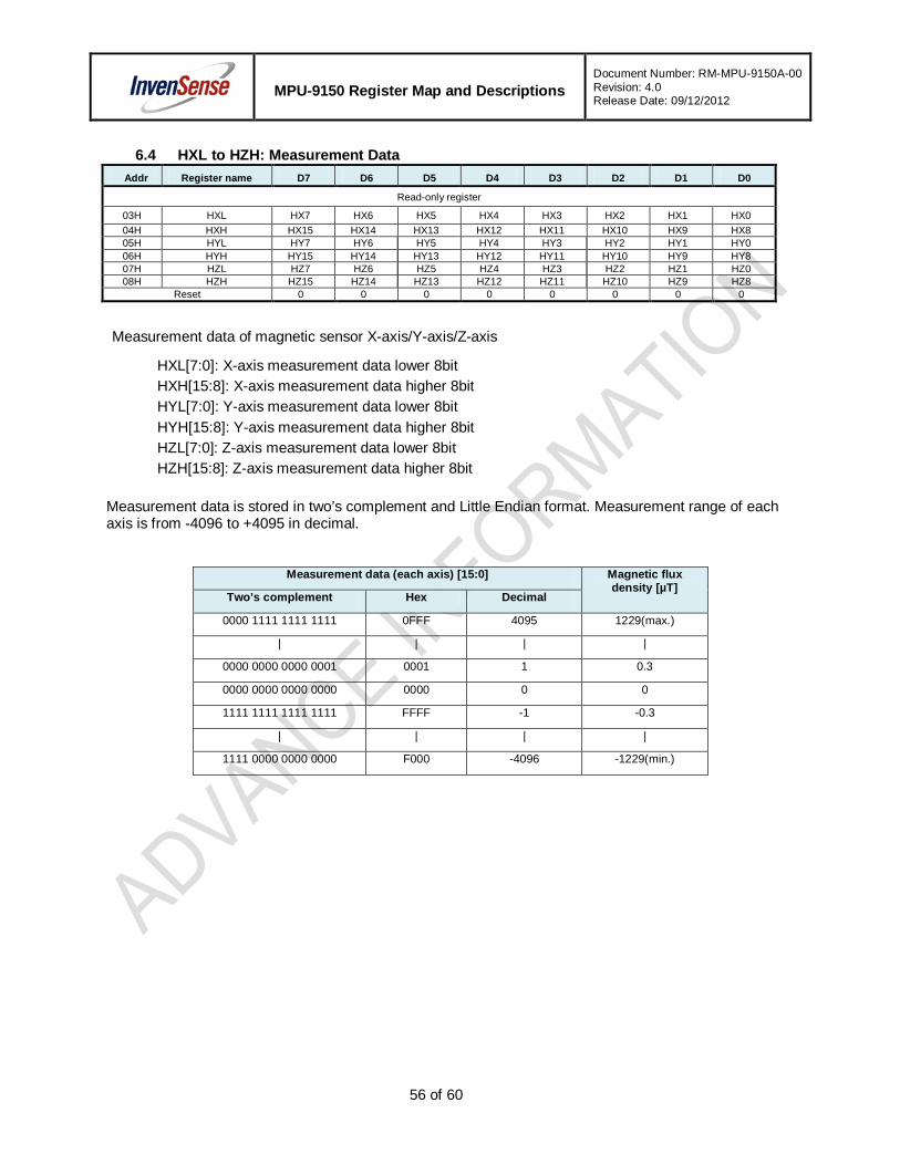
MPU-9150 Register Map and Descriptions
Document Number: RM-MPU-9150A-00 Revision: 4.0 Release Date: 09/12/2012
56 of 60
6.4 HXL to HZH: Measurement Data Addr Register name D7 D6 D5 D4 D3 D2 D1 D0
Read-only register
03H HXL HX7 HX6 HX5 HX4 HX3 HX2 HX1 HX0 04H HXH HX15 HX14 HX13 HX12 HX11 HX10 HX9 HX8 05H HYL HY7 HY6 HY5 HY4 HY3 HY2 HY1 HY0 06H HYH HY15 HY14 HY13 HY12 HY11 HY10 HY9 HY8 07H HZL HZ7 HZ6 HZ5 HZ4 HZ3 HZ2 HZ1 HZ0 08H HZH HZ15 HZ14 HZ13 HZ12 HZ11 HZ10 HZ9 HZ8
Reset 0 0 0 0 0 0 0 0
Measurement data of magnetic sensor X-axis/Y-axis/Z-axis
HXL[7:0]: X-axis measurement data lower 8bit HXH[15:8]: X-axis measurement data higher 8bit HYL[7:0]: Y-axis measurement data lower 8bit HYH[15:8]: Y-axis measurement data higher 8bit HZL[7:0]: Z-axis measurement data lower 8bit HZH[15:8]: Z-axis measurement data higher 8bit
Measurement data is stored in two’s complement and Little Endian format. Measurement range of each axis is from -4096 to +4095 in decimal.
Measurement data (each axis) [15:0] Magnetic flux
density [µT] Two’s complement Hex Decimal
0000 1111 1111 1111 0FFF 4095 1229(max.)
| | | |
0000 0000 0000 0001 0001 1 0.3
0000 0000 0000 0000 0000 0 0
1111 1111 1111 1111 FFFF -1 -0.3
| | | |
1111 0000 0000 0000 F000 -4096 -1229(min.)

MPU-9150 Register Map and Descriptions
Document Number: RM-MPU-9150A-00 Revision: 4.0 Release Date: 09/12/2012
57 of 60
6.5 ST2: Status 2 Addr Register name D7 D6 D5 D4 D3 D2 D1 D0
Read-only register 09H ST2 0 0 0 0 HOFL DERR 0 0
Reset 0 0 0 0 0 0 0 0
DERR: Data Error
"0": Normal
"1": Data read error occurred
When data reading is started out of data readable period, the read data are not correct. In this case, data read error occurs and DERR bit turns to “1”. When ST2 register is read, it returns to “0”.
HOFL: Magnetic sensor overflow
"0": Normal
"1": Magnetic sensor overflow occurred
In single measurement mode and self-test mode, magnetic sensor may overflow even though measurement data regiseter is not saturated. In this case, measurement data is not correct and HOFL bit turns to “1”. When next measurement stars, it returns to “0”.
6.6 CNTL: Control Addr Register name D7 D6 D5 D4 D3 D2 D1 D0
Read-only register 0AH CNTL 0 0 0 0 MODE3 MODE2 MODE1 MODE0
Reset 0 0 0 0 0 0 0 0
MODE[3:0]: Operation mode setting
"0000": Power-down mode "0001": Single measurement mode "1000": Self-test mode "1111": Fuse ROM access mode Other code settings are prohibited
When each mode is set, AK8975C transits to set mode.
When CNTL register is accessed to be written, registers from 02H to 09H are initialized.
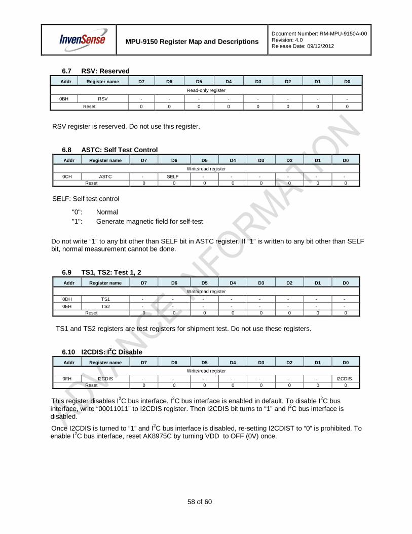
MPU-9150 Register Map and Descriptions
Document Number: RM-MPU-9150A-00 Revision: 4.0 Release Date: 09/12/2012
58 of 60
6.7 RSV: Reserved Addr Register name D7 D6 D5 D4 D3 D2 D1 D0
Read-only register
0BH RSV - - - - - - - - Reset 0 0 0 0 0 0 0 0
RSV register is reserved. Do not use this register.
6.8 ASTC: Self Test Control Addr Register name D7 D6 D5 D4 D3 D2 D1 D0
Write/read register 0CH ASTC - SELF - - - - - -
Reset 0 0 0 0 0 0 0 0
SELF: Self test control
"0": Normal "1": Generate magnetic field for self-test
Do not write “1” to any bit other than SELF bit in ASTC register. If “1” is written to any bit other than SELF bit, normal measurement cannot be done.
6.9 TS1, TS2: Test 1, 2 Addr Register name D7 D6 D5 D4 D3 D2 D1 D0
Write/read register 0DH TS1 - - - - - - - - 0EH TS2 - - - - - - - -
Reset 0 0 0 0 0 0 0 0
TS1 and TS2 registers are test registers for shipment test. Do not use these registers.
6.10 I2CDIS: I2C Disable Addr Register name D7 D6 D5 D4 D3 D2 D1 D0
Write/read register
0FH I2CDIS - - - - - - - I2CDIS Reset 0 0 0 0 0 0 0 0
This register disables I2C bus interface. I2C bus interface is enabled in default. To disable I2C bus interface, write “00011011” to I2CDIS register. Then I2CDIS bit turns to “1” and I2C bus interface is disabled.
Once I2CDIS is turned to “1” and I2C bus interface is disabled, re-setting I2CDIST to “0” is prohibited. To enable I2C bus interface, reset AK8975C by turning VDD to OFF (0V) once.

MPU-9150 Register Map and Descriptions
Document Number: RM-MPU-9150A-00 Revision: 4.0 Release Date: 09/12/2012
59 of 60
6.11 ASAX, ASAY, ASAZ: Sensitivity Adjustment values Addr Register name D7 D6 D5 D4 D3 D2 D1 D0
Read-only register 10H ASAX COEFX7 COEFX6 COEFX5 COEFX4 COEFX3 COEFX2 COEFX1 COEFX0 11H ASAY COEFY7 COEFY6 COEFY5 COEFY4 COEFY3 COEFY2 COEFY1 COEFY0 12H ASAZ COEFZ7 COEFZ6 COEFZ5 COEFZ4 COEFZ3 COEFZ2 COEFZ1 COEFZ0
Reset - - - - - - - -
Sensitivity adjustment data for each axis is stored to fuse ROM on shipment.
ASAX[7:0]: Magnetic sensor X-axis sensitivity adjustment value
ASAY[7:0]: Magnetic sensor Y-axis sensitivity adjustment value
ASAZ[7:0]: Magnetic sensor Z-axis sensitivity adjustment value
Sensitivity Adjustment
The sensitivity adjustment is done by the equation below;
( )
+
×−×= 1
1285.0128ASAHHadj ,
where H is the measurement data read out from the measurement data register, ASA is the sensitivity adjustment value, and Hadj is the adjusted measurement data.
MPU-9150 Register Map and Descriptions
Document Number: RM-MPU-9150A-00 Revision: 4.0 Release Date: 09/12/2012
60 of 60
This information furnished by InvenSense is believed to be accurate and reliable. However, no responsibility is assumed by InvenSense for its use, or for any infringements of patents or other rights of third parties that may result from its use. Specifications are subject to change without notice. InvenSense reserves the right to make changes to this product, including its circuits and software, in order to improve its design and/or performance, without prior notice. InvenSense makes no warranties, neither expressed nor implied, regarding the information and specifications contained in this document. InvenSense assumes no responsibility for any claims or damages arising from information contained in this document, or from the use of products and services detailed therein. This includes, but is not limited to, claims or damages based on the infringement of patents, copyrights, mask work and/or other intellectual property rights.
Certain intellectual property owned by InvenSense and described in this document is patent protected. No license is granted by implication or otherwise under any patent or patent rights of InvenSense. This publication supersedes and replaces all information previously supplied. Trademarks that are registered trademarks are the property of their respective companies. InvenSense sensors should not be used or sold in the development, storage, production or utilization of any conventional or mass-destructive weapons or for any other weapons or life threatening applications, as well as in any other life critical applications such as medical equipment, transportation, aerospace and nuclear instruments, undersea equipment, power plant equipment, disaster prevention and crime prevention equipment.
InvenSense®, is a registered trademark of InvenSense, Inc. MPU™, MPU-9150™, MPU-6050™, MPU-3050™, IMU-3000™, Motion Processing Unit™ , MotionFusion™, MotionProcessing™, MotionApps™, Digital Motion Processor™, Digital Motion Processing™, and DMP™ are trademarks of InvenSense, Inc.
©2011 InvenSense, Inc. All rights reserved.