MPQ2013A - Monolithic Power
19
MPQ2013A 40V, 150mA, Low Quiescent Current Linear Regulator AEC-Q100 Qualified MPQ2013A Rev. 1.07 www.MonolithicPower.com 1 8/24/2017 MPS Proprietary Information. Patent Protected. Unauthorized Photocopy and Duplication Prohibited. © 2017 MPS. All Rights Reserved. The Future of Analog IC Technology DESCRIPTION The MPQ2013A is a low power linear regulator that supplies power to systems with high voltage batteries. It includes a wide 2.5V to 40V input range, low dropout voltage and low quiescent supply current. The low quiescent current and low dropout voltage allow operations at extremely low power levels. Therefore, the MPQ2013A are ideal for the low power microcontrollers and the battery-powered equipments. The MPQ2013A provides wide variety of fixed output voltage options (if request): 1.8V, 1.9V, 2.3V, 2.5V, 3.0V, 3.3V, 3.45V, 5.0V; and also provides the output adjustable option (from 1.215V to 15V). The regulator output current is internally limited and the device is protected against over-load and over-temperature conditions. The MPQ2013A also includes thermal shutdown and current limiting fault protection, and is available in QFN-6 (2mmx2mm), and QFN-8 (3mmx3mm) packages. FEATURES 2.5V to 40V Input Range 3.3μA Quiescent Supply Current Stable With Low-value Output Ceramic Capacitor (> 0.47 μF) 150mA Specified Current for QFN-6 and QFN-8 Packages 620mV Dropout at 150mA Load Available in Fixed and Adjustable Output (1.215 V to 15 V) Versions Output ±2% Accuracy for QFN-8 Package Output ±4% Accuracy for QFN-6 Package Specified Current Limit Thermal Shutdown -40°C to +150°C Specified Junction Temperature Range Available in QFN-6 (2mmx2mm), or QFN-8 (3mmx3mm) Packages Available in AEC-Q100 Grade 1 APPLICATIONS Industrial/Automotive Applications Portable/Battery-Powered Equipment Ultra low power Microcontrollers Cellular Handsets Medical Imaging All MPS parts are lead-free and adhere to the RoHS directive. For MPS green status, please visit MPS website under Products, Quality Assurance page. “MPS” and “The Future of Analog IC Technology” are registered trademarks of Monolithic Power Systems, Inc. TYPICAL APPLICATION Output Adjustable Version Output Fixed Version
Transcript of MPQ2013A - Monolithic Power
MPQ2013A 40V, 150mA, Low Quiescent Current
Linear Regulator AEC-Q100 Qualified
MPQ2013A Rev. 1.07 www.MonolithicPower.com 1 8/24/2017 MPS Proprietary Information. Patent Protected. Unauthorized Photocopy and Duplication Prohibited. © 2017 MPS. All Rights Reserved.
The Future of Analog IC Technology
DESCRIPTION The MPQ2013A is a low power linear regulator that supplies power to systems with high voltage batteries. It includes a wide 2.5V to 40V input range, low dropout voltage and low quiescent supply current. The low quiescent current and low dropout voltage allow operations at extremely low power levels. Therefore, the MPQ2013A are ideal for the low power microcontrollers and the battery-powered equipments.
The MPQ2013A provides wide variety of fixed output voltage options (if request): 1.8V, 1.9V, 2.3V, 2.5V, 3.0V, 3.3V, 3.45V, 5.0V; and also provides the output adjustable option (from 1.215V to 15V).
The regulator output current is internally limited and the device is protected against over-load and over-temperature conditions.
The MPQ2013A also includes thermal shutdown and current limiting fault protection, and is available in QFN-6 (2mmx2mm), and QFN-8 (3mmx3mm) packages.
FEATURES
2.5V to 40V Input Range 3.3µA Quiescent Supply Current Stable With Low-value Output Ceramic
Capacitor (> 0.47 μF) 150mA Specified Current for QFN-6 and
QFN-8 Packages 620mV Dropout at 150mA Load Available in Fixed and Adjustable Output
(1.215 V to 15 V) Versions Output ±2% Accuracy for QFN-8 Package
Output ±4% Accuracy for QFN-6 Package Specified Current Limit Thermal Shutdown -40°C to +150°C Specified Junction
Temperature Range Available in QFN-6 (2mmx2mm), or QFN-8
(3mmx3mm) Packages
Available in AEC-Q100 Grade 1
APPLICATIONS Industrial/Automotive Applications Portable/Battery-Powered Equipment Ultra low power Microcontrollers Cellular Handsets Medical Imaging All MPS parts are lead-free and adhere to the RoHS directive. For MPS green status, please visit MPS website under Products, Quality Assurance page.
“MPS” and “The Future of Analog IC Technology” are registered trademarks of Monolithic Power Systems, Inc.
TYPICAL APPLICATION
Output Adjustable Version Output Fixed Version

MPQ2013A - 40V, 150mA, LOW QUIESCENT CURRENT LINEAR REGULATOR, AEC-Q100 QUALIFIED
MPQ2013A Rev. 1.07 www.MonolithicPower.com 2 8/24/2017 MPS Proprietary Information. Patent Protected. Unauthorized Photocopy and Duplication Prohibited. © 2017 MPS. All Rights Reserved.
ORDERING INFORMATION Part Number* Package Top Marking MPQ2013AGQ QFN-8 (3mmx3mm)
See Below
MPQ2013AGQ-18 QFN-8 (3mmx3mm) MPQ2013AGQ-25 QFN-8 (3mmx3mm) MPQ2013AGQ-33 QFN-8 (3mmx3mm) MPQ2013AGQ-5 QFN-8 (3mmx3mm)
MPQ2013AGQ-AEC1 QFN-8 (3mmx3mm) MPQ2013AGQ-18-AEC1 QFN-8 (3mmx3mm) MPQ2013AGQ-25-AEC1 QFN-8 (3mmx3mm) MPQ2013AGQ-33-AEC1 QFN-8 (3mmx3mm) MPQ2013AGQ-5-AEC1 QFN-8 (3mmx3mm)
* For Tape & Reel, add suffix –Z (e.g. MPQ2013AGQ–Z)
EXPOSED PADON BACKSIDE
CONNECT TO GND
QFN-8 (3mmx3mm)
TOP MARKING
AJD: part code of MPQ2013AGQ; Y: year code; LLL: lot number;
AZB: part code of MPQ2013AGQ-18; Y: year code; LLL: lot number;
AQN: part code of MPQ2013AGQ-25; Y: year code; LLL: lot number;
AJZ: part code of MPQ2013AGQ-33; Y: year code; LLL: lot number;
ALJ: part code of MPQ2013AGQ-5; Y: year code; LLL: lot number;

MPQ2013A - 40V, 150mA, LOW QUIESCENT CURRENT LINEAR REGULATOR, AEC-Q100 QUALIFIED
MPQ2013A Re v. 1.07 www.MonolithicPower.com 3 8/24/2017 MPS Proprietary Information. Patent Protected. Unauthorized Photocopy and Duplication Prohibited. © 2017 MPS. All Rights Reserved.
ORDERING INFORMATION Part Number* Package Top Marking MPQ2013AGG QFN-6 (2mmx2mm)
See Below
MPQ2013AGG-33 QFN-6 (2mmx2mm) MPQ2013AGG-5 QFN-6 (2mmx2mm)
MPQ2013AGG-AEC1 QFN-6 (2mmx2mm) MPQ2013AGG-33-AEC1 QFN-6 (2mmx2mm) MPQ2013AGG-5-AEC1 QFN-6 (2mmx2mm)
* For Tape & Reel, add suffix –Z (e.g. MPQ2013AGG–Z)
QFN-6 (2mmx2mm)
TOP MARKING
CD: part code of MPQ2013AGG; Y: year code; LLL: lot number;
CP: part code of MPQ2013AGG-33; Y: year code; LLL: lot number;
FR: part code of MPQ2013AGG-5; Y: year code; LLL: lot number;

MPQ2013A - 40V, 150mA, LOW QUIESCENT CURRENT LINEAR REGULATOR, AEC-Q100 QUALIFIED
MPQ2013A Rev. 1.07 www.MonolithicPower.com 4 8/24/2017 MPS Proprietary Information. Patent Protected. Unauthorized Photocopy and Duplication Prohibited. © 2017 MPS. All Rights Reserved.
ABSOLUTE MAXIMUM RATINGS (1) IN, EN ......................................... -0.3V to +42V OUT .............................................. -0.3V to +17V FB ................................................. -0.3V to +6V Junction Temperature ............................ +150C Lead Temperature ................................. +260C Storage Temperature ............... -65C to +150C
Continuous Power Dissipation (TA = +25°C) (2)
QFN-8(3mmx3mm) .................................. 2.08W QFN-6(2mmx2mm) .................................. 1.25W
ESD SUSCEPTIBILITY (3) HBM (Human Body Model) ..........................2kV MM (Machine Model) ............................... 200V
Recommended Operating Conditions (4) Supply Voltage VIN ........................... 2.5V to 40V Output Voltage VOUT .................... 1.215V to 15V Operating Temperature....................................... ............. TA = -40°C to +125°C, TA ≤ TJ ≤ +150°C
Thermal Resistance (5) θJA θJC QFN-6 (2mmx2mm) ................ 80 ...... 16 ... C/W QFN-8 (3mmx3mm) ................ 48 ...... 11 ... C/W
Notes: 1) Exceeding these ratings may damage the device. 2) The maximum allowable power dissipation is a function of the
maximum junction temperature TJ (MAX), the junction-to-ambient thermal resistance θJA, and the ambient temperature TA. The maximum allowable continuous power dissipation at any ambient temperature is calculated by PD (MAX) = (TJ
(MAX)-TA)/θJA. Exceeding the maximum allowable power dissipation will cause excessive die temperature, and the regulator will go into thermal shutdown. Internal thermal shutdown circuitry protects the device from permanent damage.
3) Devices are ESD sensitive. Handling precaution recommended.
4) The device is not guaranteed to function outside of its operating conditions.
5) Measured on JESD51-7, 4-layer PCB.

MPQ2013A - 40V, 150mA, LOW QUIESCENT CURRENT LINEAR REGULATOR, AEC-Q100 QUALIFIED
MPQ2013A Rev. 1.07 www.MonolithicPower.com 5 8/24/2017 MPS Proprietary Information. Patent Protected. Unauthorized Photocopy and Duplication Prohibited. © 2017 MPS. All Rights Reserved.
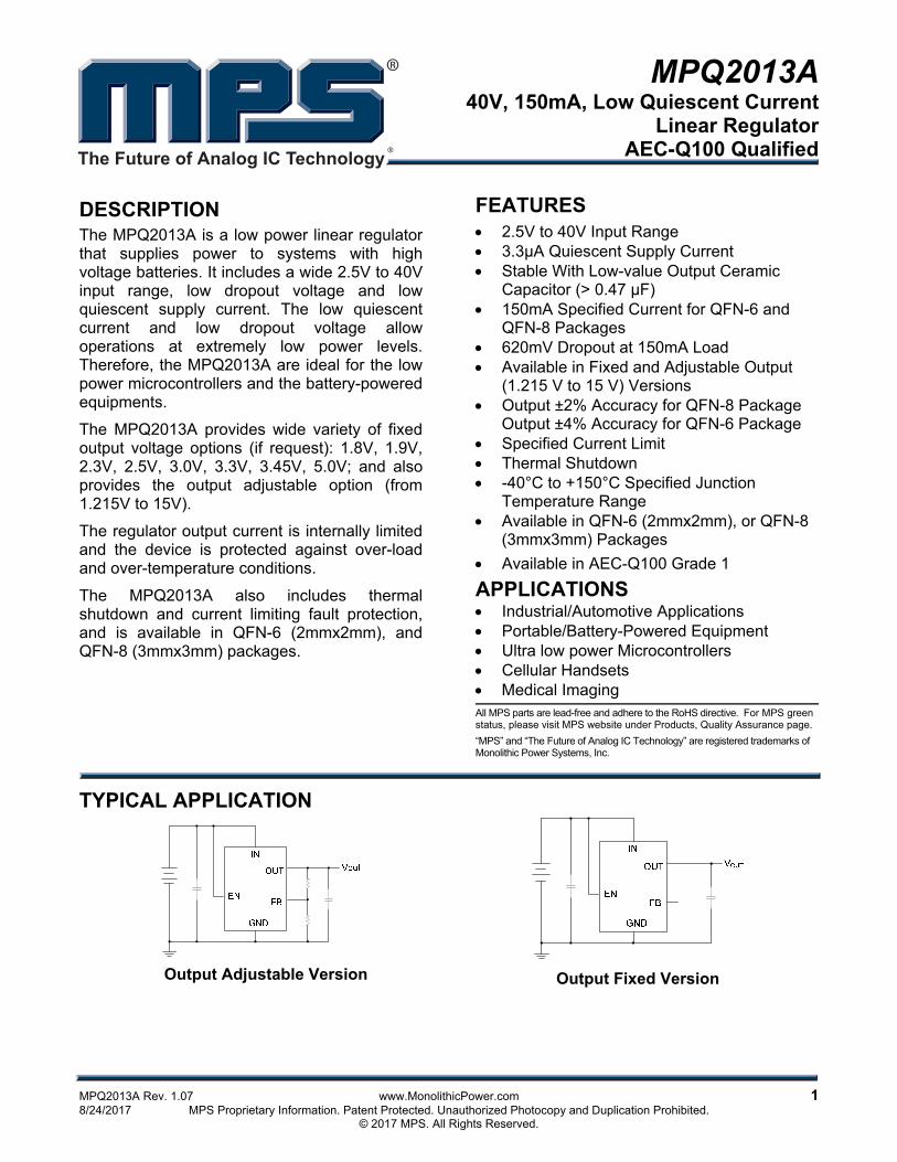
ELECTRICAL CHARACTERISTICS VEN=VIN, COUT = 1μF, TA = -40°C to +125°C, TA ≤ TJ ≤ +150°C, unless otherwise noted. Typical values are at TA = +25°C.
Parameter Symbol Condition Min Typ Max Units
Input Voltage VIN 2.5 40 V
Output Voltage Range VOUT 1.215 15 V
GND Pin Current IGND
MPQ2013AGQ, 0<IOUT<1mA, VIN=2.5V to 40V, VOUT= 5V (VIN≥6V) or FB (VIN<6V)
3.3 9
µA MPQ2013AGQ, 1mA<IOUT<30mA, VIN=2.5V to 15V, VOUT= 5V (VIN≥6V) or FB (VIN<6V)
11 22
MPQ2013AGQ, 30mA<IOUT<150mA, VIN=3V, VOUT=FB
32 50
MPQ2013AGQ-18, 0mA<IOUT<1mA,VIN=2.8V to 40V
4.4 10
µA MPQ2013AGQ-18, 1mA<IOUT<30mA,VIN=2.8V to 15V
15 25
MPQ2013AGQ-18, 30mA<IOUT<150mA, VIN=2.8V
35 50
MPQ2013AGQ-25, 0mA<IOUT<1mA,VIN=3.5V to 40V
4.4 10
µA MPQ2013AGQ-25, 1mA<IOUT<30mA,VIN=3.5V to 15V
15 25
MPQ2013AGQ-25, 30mA<IOUT<150mA, VIN=3.5V
35 50
MPQ2013AGQ-33, 0<IOUT<1mA, VIN=4.3V to 40V
4.4 10
µA MPQ2013AGQ-33, 1mA<IOUT<30mA, VIN=4.3V to 15V
15 25
MPQ2013AGQ-33, 30mA<IOUT<150mA, VIN=4.3V
35 50
MPQ2013AGQ-5, 0<IOUT<1mA, VIN=6V to 40V
4.4 10
µA MPQ2013AGQ-5 1mA<IOUT<30mA, VIN=6V to 15V
15 25
MPQ2013AGQ-5, 30mA<IOUT<150mA, VIN=6V
35 50
MPQ2013AGG, 0<IOUT<1mA, VIN=2.5V to 40V, VOUT= 5V (VIN≥6V) or FB (VIN<6V)
3.3 9
µA MPQ2013AGG, 1mA<IOUT<30mA, VIN=2.5V to 15V, VOUT= 5V (VIN≥6V) or FB (VIN<6V)
11 22
MPQ2013AGG, 30mA<IOUT<150mA, VIN=3V, VOUT=FB
32 50
MPQ2013A - 40V, 150mA, LOW QUIESCENT CURRENT LINEAR REGULATOR, AEC-Q100 QUALIFIED
MPQ2013A Rev. 1.07 www.MonolithicPower.com 6 8/24/2017 MPS Proprietary Information. Patent Protected. Unauthorized Photocopy and Duplication Prohibited. © 2017 MPS. All Rights Reserved.
ELECTRICAL CHARACTERISTICS (continued) VEN=VIN, COUT = 1μF, TA = -40°C to +125°C, TA ≤ TJ ≤ +150°C, unless otherwise noted. Typical values are at TA = +25°C.
Parameter Symbol Condition Min Typ Max Units
GND Pin Current IGND
MPQ2013AGG-33, 0<IOUT<1mA, VIN=4.3V to 40V
4.4 10
µA MPQ2013AGG-33, 1mA<IOUT<30mA, VIN=4.3V to 15V
15 25
MPQ2013AGG-33, 30mA<IOUT<150mA, VIN=4.3V
35 50
MPQ2013AGG-5, 0<IOUT<1mA, VIN=6V to 40V
4.4 10
µA MPQ2013AGG-5, 1mA<IOUT<30mA, VIN=6V to 15V
15 25
MPQ2013AGG-5, 30mA<IOUT<150mA, VIN=6V
35 50
Shutdown Supply Current
ISHDN VEN=0, VIN=2.5 to 40V 3 9 µA
Load Current Limit ILIMIT
MPQ2013AGQ, MPQ2013AGQ-5, MPQ2013AGG, MPQ2013AGG-5, VOUT = 0V, VIN=6V to 15V
160 270 400 mA MPQ2013AGQ-33, MPQ2013AGG-33, VOUT = 0V, VIN=4.3V to 15V
MPQ2013AGQ-18, VOUT=0V,VIN=3.5V to 15V
MPQ2013AGQ-25, VOUT=0V,VIN=3.5V to 15V
Output Voltage Accuracy
MPQ2013AGQ-18,VIN=2.8V,IOUT=0 1.746 1.8 1.854
V
MPQ2013AGQ-18,VIN=2.8V,IOUT=0, TA = +25°C
1.773 1.8 1.827
MPQ2013AGQ-25,VIN=3.5V,IOUT=0 2.45 2.5 2.55
MPQ2013AGQ-33,VIN =4.3V, IOUT=0 3.234 3.3 3.366
MPQ2013AGQ-5,VIN=6V, IOUT=0 4.9 5 5.1
MPQ2013AGG-33,VIN=4.3V,IOUT=0 3.168 3.3 3.432
MPQ2013AGG-33,VIN=4.3V,IOUT=0, TA = +25°C
3.251 3.3 3.349
MPQ2013AGG-5,VIN=6V,IOUT=0 4.8 5 5.2
MPQ2013AGG-5,VIN=6V,IOUT=0, TA = +25°C
4.925 5 5.075
FB Voltage VFB
MPQ2013AGQ, MPQ2013AGQ-25, MPQ2013AGQ-33, MPQ2013AGQ-5, VOUT=FB, VIN=5V, IOUT=0
1.191 1.215 1.239V
MPQ2013AGQ-18, VOUT=FB, VIN=5V, IOUT=0
1.179 1.215 1.251
MPQ2013AGQ-18, VOUT=FB, VIN=5V, IOUT=0 TA = +25°C
1.197 1.215 1.233
MPQ2013A - 40V, 150mA, LOW QUIESCENT CURRENT LINEAR REGULATOR, AEC-Q100 QUALIFIED
MPQ2013A Re v. 1.07 www.MonolithicPower.com 7 8/24/2017 MPS Proprietary Information. Patent Protected. Unauthorized Photocopy and Duplication Prohibited. © 2017 MPS. All Rights Reserved.
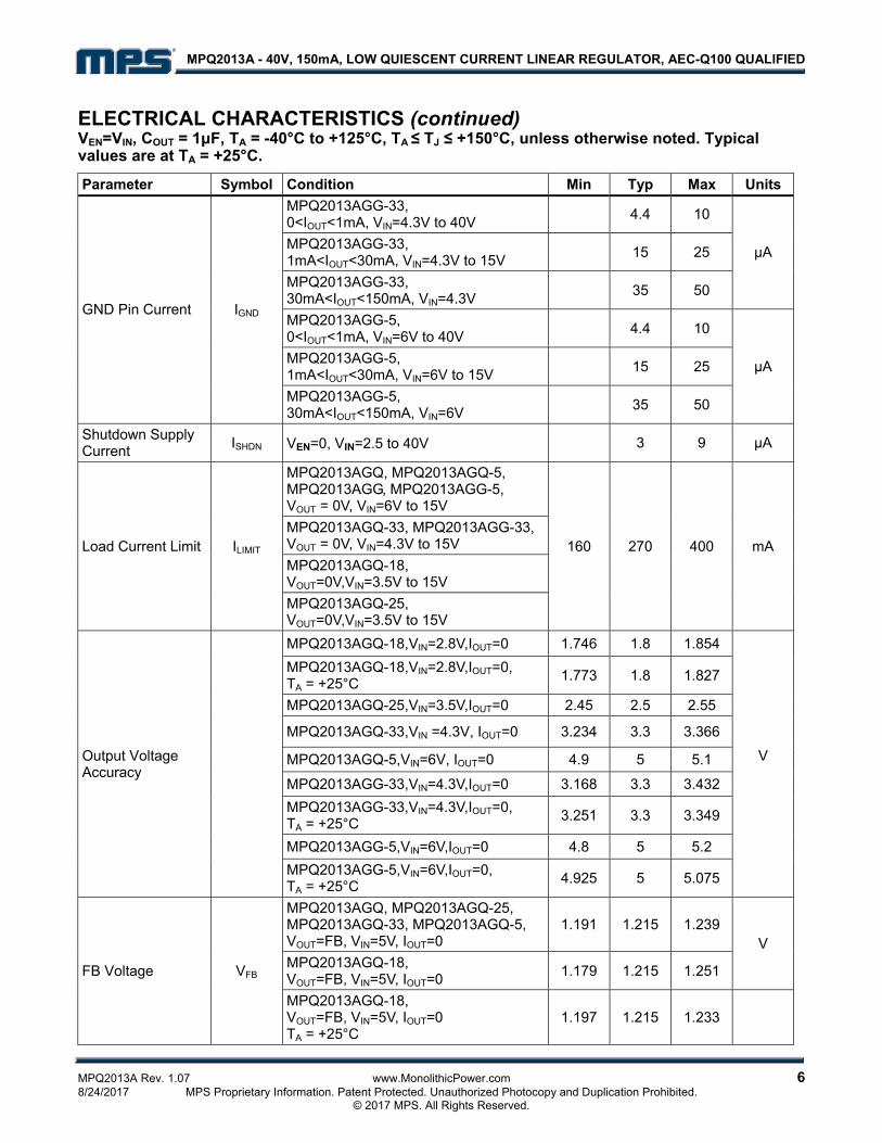
ELECTRICAL CHARACTERISTICS (continued) VEN=VIN, COUT = 1μF, TA = -40°C to +125°C, TA ≤ TJ ≤ +150°C, unless otherwise noted. Typical values are at TA = +25°C.
Parameter Symbol Condition Min Typ Max Units
FB Voltage VFB
MPQ2013AGG, MPQ2013AGG-33, MPQ2013AGG-5, VOUT=FB,VIN=6V,IOUT=0,
1.167 1.215 1.263
V MPQ2013AGG, MPQ2013AGG-33, MPQ2013AGG-5, VOUT=FB,VIN=6V,IOUT=0, TA = +25°C
1.197 1.215 1.233
Dropout Voltage VIN=VOUT(NOM)-0.1V
VDROPOUT
MPQ2013AGQ, MPQ2013AGQ-5, MPQ2013AGG, MPQ2013AGG-5, IOUT=150mA, VOUT(NOM)=5V
600 1100
mV
MPQ2013AGQ-33, IOUT=150mA, VOUT(NOM)=3.3V
700 1100
MPQ2013AGQ-25, IOUT=150mA, VOUT(NOM)=2.5V
700 1300
MPQ2013AGQ-18, IOUT=100mA, VOUT(NOM)=1.8V
700 1100
MPQ2013AGG-33, IOUT=150mA, VOUT(NOM)=3.3V
700 1300
FB Pin Input Current
IFB
MPQ2013A-18, MPQ2013A-25, MPQ2013A-33, MPQ2013A-5, VFB=1.3V, VIN=6V, OUT Floating
0.88 1.3 1.72 μA
MPQ2013A, VFB=1.3V, VIN=6V, OUT Floating
-50 0 50 nA
Line Regulation(6) VIN = 2.5 to 40V, IOUT = 1mA, OUT = FB
0.01 0.05 %/V
Load Regulation(7)
MPQ2013AGQ IOUT = 100μA to 150mA, VIN=3V to 6V
0.005
0.012
%/mA
MPQ2013AGQ-18, IOUT = 100μA to 150mA, VIN=6V
0.020
MPQ2013AGQ-25, IOUT = 100μA to 150mA, VIN=3.5V to 6V
0.020
MPQ2013AGQ-33, IOUT = 100μA to 150mA, VIN=4.3V to 6V
0.015
MPQ2013AGQ-5, IOUT = 100μA to 150mA, VIN=6V
0.012
MPQ2013AGG IOUT = 100μA to 150mA, VIN=3V to 6V
0.012
MPQ2013AGG-33, IOUT = 100μA to 150mA, VIN=4.3V to 6V
0.020
MPQ2013AGG-5, IOUT = 100μA to 150mA, VIN= 6V
0.012

MPQ2013A - 40V, 150mA, LOW QUIESCENT CURRENT LINEAR REGULATOR, AEC-Q100 QUALIFIED
MPQ2013A Rev. 1.07 www.MonolithicPower.com 8 8/24/2017 MPS Proprietary Information. Patent Protected. Unauthorized Photocopy and Duplication Prohibited. © 2017 MPS. All Rights Reserved.
ELECTRICAL CHARACTERISTICS (continued) VEN=VIN, COUT = 1μF, TA = -40°C to +125°C, TA ≤ TJ ≤ +150°C, unless otherwise noted. Typical values are at TA = +25°C.
Parameter Symbol Condition Min Typ Max Units
Output Voltage PSRR(8)
100Hz, CIN = 100pF, COUT = 4.7μF IOUT=10mA, VIN=6V, VOUT=5V
58 dB
1kHz, CIN = 100pF, COUT = 4.7μF IOUT=10mA, VIN=6V, VOUT=5V
41 dB
100kHz, CIN = 100pF, COUT = 4.7μF IOUT=10mA, VIN=6V, VOUT=5V
55 dB
Startup Response Time
MPQ2013AGQ, MPQ2013AGG, IOUT=100mA, COUT=6.8μF, VOUT=5V
3
ms
MPQ2013AGQ-18, IOUT=10mA, COUT=6.8μF, VOUT=1.8V
1.1
MPQ2013AGQ-25, IOUT=10mA, COUT=6.8μF, VOUT=2.5V
1.5
MPQ2013AGQ-33, MPQ2013AGG-33, IOUT=10mA, COUT=6.8μF, VOUT=3.3V
1.8
MPQ2013AGQ-5, MPQ2013AGG-5, IOUT=10mA,COUT=6.8μF,VOUT=5V
3
EN Rising Threshold
ENTH_R VIN=2.5V to 40V 1.32 1.48 1.64 V
EN Falling Threshold
ENTH_F VIN=2.5V to 40V 1.1 1.26 1.42 V
EN Pin Input Current
IEN VEN = 0V or 15V, VIN=2.5V to 40V 0.1 μA
Thermal Shutdown(8)
TSD 150 165 C
Thermal Shutdown Hysteresis(8)
∆TSD 20 C
Notes:
6) IN(MAX ) IN(MIN)OUT[V ] OUT[V ]
IN(MAX) IN(MIN) OUT(NOM)
| V V |Line Regulation= (% / V)
(V V ) V
7) OUT(MAX) OUT(MIN)OUT[I ] OUT[I ]
OUT(MAX) OUT(MIN) OUT(NOM)
| V V |Load Regulation= (%/mA)
(I I ) V
8) Derived from bench characterization. Not tested in production.
MPQ2013A - 40V, 150mA, LOW QUIESCENT CURRENT LINEAR REGULATOR, AEC-Q100 QUALIFIED
MPQ2013A Rev. 1.07 www.MonolithicPower.com 9 8/24/2017 MPS Proprietary Information. Patent Protected. Unauthorized Photocopy and Duplication Prohibited. © 2017 MPS. All Rights Reserved.
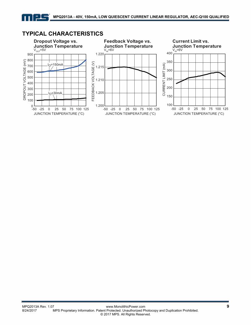
TYPICAL CHARACTERISTICS
MPQ2013A - 40V, 150mA, LOW QUIESCENT CURRENT LINEAR REGULATOR, AEC-Q100 QUALIFIED
MPQ2013A Rev. 1.07 www.MonolithicPower.com 10 8/24/2017 MPS Proprietary Information. Patent Protected. Unauthorized Photocopy and Duplication Prohibited. © 2017 MPS. All Rights Reserved.
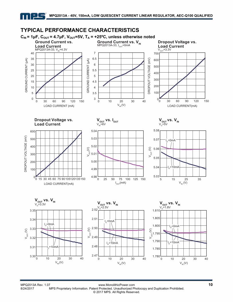
TYPICAL PERFORMANCE CHARACTERISTICS CIN = 1μF, COUT = 4.7μF, VOUT=5V, TA = +25ºC, unless otherwise noted

MPQ2013A - 40V, 150mA, LOW QUIESCENT CURRENT LINEAR REGULATOR, AEC-Q100 QUALIFIED
MPQ2013A Rev. 1.07 www.MonolithicPower.com 11 8/24/2017 MPS Proprietary Information. Patent Protected. Unauthorized Photocopy and Duplication Prohibited. © 2017 MPS. All Rights Reserved.
TYPICAL PERFORMANCE CHARACTERISTICS (continued) CIN = 1μF, COUT = 4.7μF, VOUT=5V, TA = +25ºC, unless otherwise noted
MPQ2013A - 40V, 150mA, LOW QUIESCENT CURRENT LINEAR REGULATOR, AEC-Q100 QUALIFIED
MPQ2013A Rev. 1.07 www.MonolithicPower.com 12 8/24/2017 MPS Proprietary Information. Patent Protected. Unauthorized Photocopy and Duplication Prohibited. © 2017 MPS. All Rights Reserved.
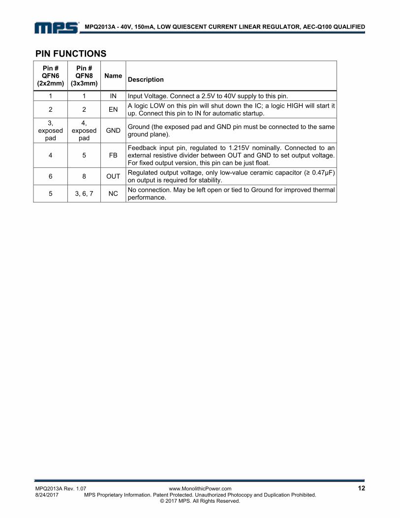
PIN FUNCTIONS
Pin # QFN6
(2x2mm)
Pin # QFN8
(3x3mm) Name
Description
1 1 IN Input Voltage. Connect a 2.5V to 40V supply to this pin.
2 2 EN A logic LOW on this pin will shut down the IC; a logic HIGH will start it up. Connect this pin to IN for automatic startup.
3, exposed
pad
4, exposed
pad GND
Ground (the exposed pad and GND pin must be connected to the same ground plane).
4 5 FB Feedback input pin, regulated to 1.215V nominally. Connected to an external resistive divider between OUT and GND to set output voltage. For fixed output version, this pin can be just float.
6 8 OUTRegulated output voltage, only low-value ceramic capacitor (≥ 0.47μF) on output is required for stability.
5 3, 6, 7 NC No connection. May be left open or tied to Ground for improved thermal performance.

MPQ2013A - 40V, 150mA, LOW QUIESCENT CURRENT LINEAR REGULATOR, AEC-Q100 QUALIFIED
MPQ2013A Rev. 1.07 www.MonolithicPower.com 13 8/24/2017 MPS Proprietary Information. Patent Protected. Unauthorized Photocopy and Duplication Prohibited. © 2017 MPS. All Rights Reserved.
OPERATIONThe MPQ2013A is a linear regulator that supplies power to systems with high voltage batteries. It includes a wide 2.5V to 40V input range, low dropout voltage and low quiescent supply current.
The MPQ2013A provides wide variety of fixed output voltage options: 1.8V, 1.9V, 2.3V, 2.5V, 3.0V, 3.3V, 3.45V, 5.0V; and also provides the output adjustable option (from 1.215V to 15V).
The output adjustable version has an output that is adjustable from 1.215V to 15V with a simple resistor divider. It uses external feedback, allowing the user to set the output voltage with an external resistor divider. The typical FB pin voltage is 1.215V.
The IC enters shutdown mode when EN is low. In shutdown mode, the pass transistor, control circuitry, reference and all biases turn off, reducing the supply current to <3µA. Connect EN pin to IN for automatic startup.
The regulator output current is internally limited and the device is protected against over-load and over-temperature conditions.
The peak output current is limited to around 270mA, which exceeds the 150mA recommended continuous output current.
When the junction temperature is too high, the thermal sensor sends a signal to the control logic that will shutdown the IC. The IC will restart when the temperature has sufficiently cooled.
The maximum power output current is a function of the package’s maximum power dissipation for a given temperature.
The maximum power dissipation is dependent on the thermal resistance of the case and the circuit board, the temperature difference between the die junction and the ambient air, and the rate of air flow. The GND pin and Exposed Pad must be connected to the ground plane for proper dissipation.
UVLO Vreference
EA
VIN
EN
VOUT
FBGND
For fixed output version only
Figure 1: Functional Block Diagram

MPQ2013A - 40V, 150mA, LOW QUIESCENT CURRENT LINEAR REGULATOR, AEC-Q100 QUALIFIED
MPQ2013A Rev. 1.07 www.MonolithicPower.com 14 8/24/2017 MPS Proprietary Information. Patent Protected. Unauthorized Photocopy and Duplication Prohibited. © 2017 MPS. All Rights Reserved.
APPLICATION INFORMATION Component Selection
Setting the Output Voltage Set the output voltage of the MPQ2013A by using a resistor divider as shown:
Figure 2: FB Resistor Divider to Set VOUT
Choose R2=1MΩ to maintain a 1.215µA minimum load. Calculate the value for R1 using the following equation:
11.215V
VR2R1 OUT
For fixed output version, VOUT also can be adjusted by adding external resistor divider. Just note to take internal FB resistor divider into consideration when choose external divider.
Figure 3: FB Divider of Fixed Output Version
When R2 is selected, R1 can be calculated by below equation:
OUT
R1_INR1
1.215xR1_INx(R2 R2 _IN)1
(V 1.215)xR2xR2 _IN
The internal FB resistor dividers for different fixed output versions please see below table.
Table 1: Internal FB Resistor Divider
Fixed Output Voltage (V)
R1_IN (MΩ) R2_IN (MΩ)
2.5 1.058 1 3.3 1.716 1 5 3.117 1
Table 2 is an example of external FB divider to get various output voltages on fixed 3.3V output version.
Table 2 –3.3V Fixed Output Version External FB Divider
VOUT (V) R1 (kΩ) R2 (kΩ)
11 84.5 10
8.5 61.9 10
8 57.6 10
6.5 44.2 10
5 31.6 10
Setting VIN UVLO To prevent part from operating at an insufficient power supply voltage, a resistor divider as show in figure 3 can be used to adjust the VIN UVLO point.
Figure 4: EN Resistor Divider to Set VIN UVLO
If choose R3 first, then R4 can be calculated by below equation:
TH_L_UVLOIN
TH_L
ENV
ENR3R4
Where ENTH_L is the EN falling threshold 1.26V. To limit the divider current, high value resistors are recommended. For example, if VIN_UVLO is set at 4.5V, R3=2MΩ and R4=778kΩ can be used.
MPQ2013A - 40V, 150mA, LOW QUIESCENT CURRENT LINEAR REGULATOR, AEC-Q100 QUALIFIED
MPQ2013A Rev. 1.07 www.MonolithicPower.com 15 8/24/2017 MPS Proprietary Information. Patent Protected. Unauthorized Photocopy and Duplication Prohibited. © 2017 MPS. All Rights Reserved.
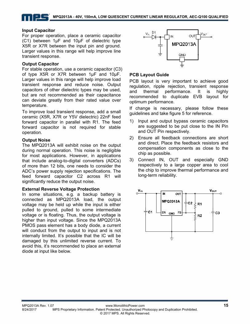
Input Capacitor For proper operation, place a ceramic capacitor (C1) between 1µF and 10µF of dielectric type X5R or X7R between the input pin and ground. Larger values in this range will help improve line transient response.
Output Capacitor For stable operation, use a ceramic capacitor (C3) of type X5R or X7R between 1µF and 10µF. Larger values in this range will help improve load transient response and reduce noise. Output capacitors of other dielectric types may be used, but are not recommended as their capacitance can deviate greatly from their rated value over temperature.
To improve load transient response, add a small ceramic (X5R, X7R or Y5V dielectric) 22nF feed forward capacitor in parallel with R1. The feed forward capacitor is not required for stable operation.
Output Noise The MPQ2013A will exhibit noise on the output during normal operation. This noise is negligible for most applications. However, in applications that include analog-to-digital converters (ADCs) of more than 12 bits, one needs to consider the ADC’s power supply rejection specifications. The feed forward capacitor C2 across R1 will significantly reduce the output noise.
External Reverse Voltage Protection In some situations, e.g. a backup battery is connected as MPQ2013A load, the output voltage may be held up while the input is either pulled to ground, pulled to some intermediate voltage or is floating. Thus, the output voltage is higher than input voltage. Since the MPQ2013A PMOS pass element has a body diode, a current will conduct from the output to input and is not internally limited. It’s possible that the IC will be damaged by this unlimited reverse current. To avoid this, it’s recommended to place an external diode at input like below.
PCB Layout Guide
PCB layout is very important to achieve good regulation, ripple rejection, transient response and thermal performance. It is highly recommended to duplicate EVB layout for optimum performance.
If change is necessary, please follow these guidelines and take figure 5 for reference.
1) Input and output bypass ceramic capacitors are suggested to be put close to the IN Pin and OUT Pin respectively.
2) Ensure all feedback connections are short and direct. Place the feedback resistors and compensation components as close to the chip as possible.
3) Connect IN, OUT and especially GND respectively to a large copper area to cool the chip to improve thermal performance and long-term reliability.

MPQ2013A - 40V, 150mA, LOW QUIESCENT CURRENT LINEAR REGULATOR, AEC-Q100 QUALIFIED
MPQ2013A Re v. 1.07 www.MonolithicPower.com 16 8/24/2017 MPS Proprietary Information. Patent Protected. Unauthorized Photocopy and Duplication Prohibited. © 2017 MPS. All Rights Reserved.
Figure 5: PCB Layout (Top Layer)
Design Example
Below is a design example following the application guidelines for VOUT=3.3V with feedforward cap.
Figure 6: Design Example

MPQ2013A - 40V, 150mA, LOW QUIESCENT CURRENT LINEAR REGULATOR, AEC-Q100 QUALIFIED
MPQ2013A Rev. 1.07 www.MonolithicPower.com 17 8/24/2017 MPS Proprietary Information. Patent Protected. Unauthorized Photocopy and Duplication Prohibited. © 2017 MPS. All Rights Reserved.
TYPICAL APPLICATION CIRCUITS
R1
R2C2C1
IN
EN GND FB
OUTVIN VOUT
1uF 4.7uF
1.72MΩ
1MΩ
3.3V
MPQ2013A
Figure 7: 3.3V Output Typical Application Circuit
Figure 8: 3.3V Output with Feedforward Capacitor
R1
R2C2C1
IN
EN GND FB
OUTVIN VOUT
1uF 4.7uF
3.1MΩ
1MΩ
5V
MPQ2013A
Figure 9: 5V Output Typical Application Circuit

MPQ2013A - 40V, 150mA, LOW QUIESCENT CURRENT LINEAR REGULATOR, AEC-Q100 QUALIFIED
MPQ2013A Rev. 1.07 www.MonolithicPower.com 18 8/24/2017 MPS Proprietary Information. Patent Protected. Unauthorized Photocopy and Duplication Prohibited. © 2017 MPS. All Rights Reserved.
PACKAGE INFORMATION
QFN-8 (3mmx3mm)
SIDE VIEW
TOP VIEW
18
5 4
BOTTOM VIEW
2.903.10
1.451.75
2.903.10
2.252.55
0.65BSC
0.200.30
0.801.00
0.000.05
0.20 REF
PIN 1 IDMARKING
1.70
0.65
0.25
RECOMMENDED LAND PATTERN
2.90NOTE:
1) ALL DIMENSIONS ARE IN MILLIMETERS. 2) EXPOSED PADDLE SIZE DOES NOT INCLUDE MOLD FLASH. 3) LEAD COPLANARITY SHALL BE 0.10 MILLIMETER MAX. 4) JEDEC REFERENCE IS MO-229, VARIATION VEEC-2. 5) DRAWING IS NOT TO SCALE.
PIN 1 IDSEE DETAIL A
2.50
0.70
PIN 1 ID OPTION BR0.20 TYP.
PIN 1 ID OPTION A0.30x45º TYP.
DETAIL A
0.300.50
PIN 1 IDINDEX AREA

MPQ2013A - 40V, 150mA, LOW QUIESCENT CURRENT LINEAR REGULATOR, AEC-Q100 QUALIFIED
NOTICE: The information in this document is subject to change without notice. Please contact MPS for current specifications. Users should warrant and guarantee that third party Intellectual Property rights are not infringed upon when integrating MPS products into any application. MPS will not assume any legal responsibility for any said applications.
MPQ2013A Rev. 1.07 www.MonolithicPower.com 19 8/24/2017 MPS Proprietary Information. Patent Protected. Unauthorized Photocopy and Duplication Prohibited. © 2017 MPS. All Rights Reserved.
QFN-6 (2mmx2mm)
SIDE VIEW
TOP VIEW
16
43
BOTTOM VIEW
1.902.10
0.650.85
1.902.10
1.251.45
0.65BSC
0.200.30
0.801.00
0.000.05
0.20 REF
PIN 1 IDMARKING
0.70
0.65
0.25
RECOMMENDED LAND PATTERN
1.90 NOTE:
1) ALL DIMENSIONS ARE IN MILLIMETERS. 2) EXPOSED PADDLE SIZE DOES NOT INCLUDE MOLD FLASH. 3) LEAD COPLANARITY SHALL BE 0.10 MILLIMETER MAX. 4) JEDEC REFERENCE IS MO-229, VARIATION VCCC. 5) DRAWING IS NOT TO SCALE.
PIN 1 IDSEE DETAIL A
1.40
0.70
PIN 1 ID OPTION A0.30x45º TYP.
PIN 1 ID OPTION BR0.20 TYP.
DETAIL A
0.300.40
PIN 1 IDINDEX AREA