MPC8548ERMAD, Errata to MPC8548E PowerQUICC III Integrated ... · This document describes...
94
Freescale Semiconductor Addendum © 2010-2013 Freescale Semiconductor, Inc. All rights reserved. This document describes corrections to the MPC8548E PowerQUICC III Integrated Host Processor Family Reference Manual, Revision 2. For convenience, the section number and page number of the errata item in the reference manual are provided. Items in bold are new since the last revision of this document. To locate published updates for this document, see the website on the back page of this document. Section, Page No. Changes 1.2.1, 1-6 In bullet “Local bus controller (LBC),” replace first sub-bullet with the following: Multiplexed 32-bit address and data bus operating at up to 133 MHz. 2.4, 2-28 In Table 2-11, “Memory Map,” change L2ERRADDRL offset to 0x2_0E50 and change L2ERRADDRH offset to 0x2_0E54. 3.2, 3-19 In Table 3-3 “MPC8548E Reset Configuration Signals,” add the following footnote to all instances of “Must be driven”: “Internal pull ups pull up the signal, but an ‘all ones’ configuration is not valid, and the signal should be driven with an external circuit or pulled down to ensure proper operation.” 3.3, 3-21 In Table 3-4, “Output Signal States During System Reset,” change MCK/MCK_B state during HRESET from “Driven Toggling” to “Driven”, change TSEC[1:4]_TX_EN state during HRESET from “Driven Low” to “Hi-Z”, and change CLK_OUT state during HRESET from “Driven Toggling” to “Hi-Z”. 3.3, 3-21 In Table 3-4, “Output Signal States During System Reset,” remove TSEC3_TXD6/TSEC4_TXD2 from row that previously contained TSEC3_TXD[7:6]/TSEC4_TXD[3:2], as follows: Document Number: MPC8548ERMAD Rev. 2.4, 04/2013 Errata to MPC8548E PowerQUICC III Integrated Host Processor Family Reference Manual, Rev. 2
Transcript of MPC8548ERMAD, Errata to MPC8548E PowerQUICC III Integrated ... · This document describes...

Freescale SemiconductorAddendum
© 2010-2013 Freescale Semiconductor, Inc. All rights reserved.
This document describes corrections to the MPC8548E PowerQUICC III Integrated Host Processor Family Reference Manual, Revision 2. For convenience, the section number and page number of the errata item in the reference manual are provided. Items in bold are new since the last revision of this document.
To locate published updates for this document, see the website on the back page of this document.
Section, Page No. Changes
1.2.1, 1-6 In bullet “Local bus controller (LBC),” replace first sub-bullet with the following:Multiplexed 32-bit address and data bus operating at up to 133 MHz.
2.4, 2-28 In Table 2-11, “Memory Map,” change L2ERRADDRL offset to 0x2_0E50 and change L2ERRADDRH offset to 0x2_0E54.
3.2, 3-19 In Table 3-3 “MPC8548E Reset Configuration Signals,” add the following footnote to all instances of “Must be driven”: “Internal pull ups pull up the signal, but an ‘all ones’ configuration is not valid, and the signal should be driven with an external circuit or pulled down to ensure proper operation.”
3.3, 3-21 In Table 3-4, “Output Signal States During System Reset,” change MCK/MCK_B state during HRESET from “Driven Toggling” to “Driven”, change TSEC[1:4]_TX_EN state during HRESET from “Driven Low” to “Hi-Z”, and change CLK_OUT state during HRESET from “Driven Toggling” to “Hi-Z”.
3.3, 3-21 In Table 3-4, “Output Signal States During System Reset,” remove TSEC3_TXD6/TSEC4_TXD2 from row that previously contained TSEC3_TXD[7:6]/TSEC4_TXD[3:2], as follows:
Document Number: MPC8548ERMADRev. 2.4, 04/2013
Errata to MPC8548EPowerQUICC IIIIntegrated Host ProcessorFamily Reference Manual, Rev. 2

Section, Page No. Changes
Errata to MPC8548E PowerQUICC III Integrated Host Processor Family Reference Manual, Rev. 2
2 Freescale Semiconductor
4.3.1.1.2, 4-6 In Table 4-5, “CCSRBAR Bit Settings,” add clarification for BASE_ADDR (bits 8–23) field description to say the following: “Identifies the 16 most significant address bits of the 36-bit window.”
4.4.2.1, 4-27 Append the following sentence to the first paragraph and remove the remainder of the section:“See the MPC8548E Integrated Processor Hardware Specifications for specific supported frequencies.
4.4.3.1, 4-11 In Table 4-9, “CCB Clock PLL Ratio,” add the following footnote: “A weak pull-up resistor is present.”In addition, remove “no default” designation for System PLL Ratio POR configuration signals.Designated “default (111)”
Table 3-4. Output Signal States During System Reset
Interface Signal State During Reset
TSEC3/TSEC41
1 ...
TSEC3_TXD7/TSEC4_TXD3 Input—reset config (test only)2
2 Test-mode input during reset; must not be pulled low.

Section, Page No. Changes
Errata to MPC8548E PowerQUICC III Integrated Host Processor Family Reference Manual, Rev. 2
Freescale Semiconductor 3
4.4.3.4, 4-13 Replace Table 4-12, “Host/Agent Configuration,” with the following:
4.4.3.18, 4-21 In body text, Table 4-27, “PCI1 Speed Configuration,” and Table 4-28, “PCI2 Speed Configuration,” changed references of 33 MHz to 33.33 MHz and 66 MHZ to 66.66 MHZ.
5.2, 5-5 In Table 5-1, “Device Revision Level Cross-Reference,” add row for 2.1 silicon.
Table 4-12. Host/Agent Configuration
Functional SignalsReset Configuration
NameValue
(Binary) Meaning
LWE[1:3]/LBS[1:3]
Default (111)
cfg_host_agt[0:2] 000 PCI1/PCI-X: hostPCI2: hostPCI Express: endpointSerial RapidIO: agent
x01 PCI1/PCI-X: hostPCI2: hostPCI Express: root complexSerial RapidIO: agent
010 PCI1/PCI-X: hostPCI2: hostPCI Express: endpointSerial RapidIO: host
011 Reserved
100 PCI1/PCI-X: agentPCI2: agentPCI Express: root complexSerial RapidIO: agent
110 PCI1/PCI-X: agentPCI2: agentPCI Express: root complexSerial RapidIO: host
111 (default)PCI1/PCI-X: hostPCI2: hostPCI Express: root complexSerial RapidIO: host

Section, Page No. Changes
Errata to MPC8548E PowerQUICC III Integrated Host Processor Family Reference Manual, Rev. 2
4 Freescale Semiconductor
5.3, 5-8 Modify Figure 5-3, “Four-Stage MU Pipeline, Showing Divide Bypass,” and change title to “MU Pipeline, Showing Divide Bypass,” as follows:
Figure 5-3. MU Pipeline, Showing Divide Bypass
In addition, add the following text to the first bullet under the MU features:“Six-cycle latency for double-precision multiplication.”
6.10.2, 6-26 In Figure 6-33, “Hardware Implementation-Dependent Register 1 (HID1),” change access from “Supervisor read/write” to “Supervisor Mixed.”
6.10.2, 6-26 In Table 6-19, “HID1 Field Descriptions,” change reset value of PLL_MODE (bits 32–33) to 11.In same section, update PLL_CFG (bits 34–39) to show all supported values, as follows:0000_10Ratio of 1:10000_11Ratio of 3:2....0010_00Ratio of 4:10010_01Ratio of 9:2 (4.5:1)
7.3, 7-9 In Table 7-3, “L2/SRAM Memory-Mapped Registers,” change offsets for L2ERRADDRH and L2ERRADDRL to read as follows:
Table 7-3. L2/SRAM Memory-Mapped Registers
Offset Register Access Reset Section/Page
0x2_0E50 L2ERRADDRL—L2 error address capture register low R All zeros 7.3.1.4.2/7-20
0x2_0E54 L2ERRADDRH—L2 error address capture register high R All zeros 7.3.1.4.2/7-20
Upper Lower
MU-3
MU-1
MU-2
Divide Bypass Path
Postdivide
Divide
ReservationStation
From GIQ0 or GIQ1
MU-4
Upper Lower
MU-3
MU-1
MU-4
MU-2
Divide
Divide
Predivide
Bypass
MU-3
MU-1
MU-4
MU-2
Divide
Divide
Predivide
Bypass
MU-5
MU-6
Double Precision

Section, Page No. Changes
Errata to MPC8548E PowerQUICC III Integrated Host Processor Family Reference Manual, Rev. 2
Freescale Semiconductor 5
7.3.1.4.2, 7-24 In Figure 7-23, “L2 Error Address Capture Register (L2ERRADDRH),” change the offset to 0x2_0E54. Also, in Figure 7-24, “L2 Error Address Capture Register (L2ERRADDRL),” change the offset to 0x2_0E50.
8.4, 8-10 Change first sentence of second paragraph to the following:If any device other than the e500 core (such as PCI) is used to initialize the device, the CPU boot configuration power-on reset pin should be pulled low to initially clear EEBPCR[CPU_EN].
8.4/8-10 Change the last paragraph to the following:EEBACR[A_STRM_CNT] allows users to balance response latency with throughput and should prove useful in tuning systems with multiple time-critical tasks. The default value of 0b11 causes the ECM to attempt to stream as many as four transactions initiated from the same CCB master. Decreasing this value decreases the maximum number of transactions that may be streamed together from any one CCB master. Decreasing this value can decrease throughput for high priority transactions, but may decrease latency for lower priority transactions from another CCB master. Note that the e500 core must also have streaming enabled (through HID1[ASTME]) for the CCB to stream.
9.1, 9-1 Make MCS signal active-low in Figure 9-1. 9.3.2.1, 9-7 In Table 9-3, “Memory Interface Signals—Detailed Signal Descriptions,” modify
the description of the signal description of MA[15:0] to say the following:“Assertion/Negation—The address lines are only driven when the controller has a command scheduled to issue on the address/CMD bus; otherwise they will be at high-Z. It is valid when a transaction is driven to DRAM (when MCSn is active).”
9.3.2.2, 9-9 In Table 9-4, “Clock Signals—Detailed Signal Descriptions,” update MCKE description to add the following:“The MCKE signals should be connected to the same rank of memory as the corresponding MCS and MODT signals. For example, MCKE[0] should be connected to the same rank of memory as MCS[0] and MODT[0].”
9.4.1.3, 9-14 In Table 9-8, “TIMING_CFG_3 Field Descriptions,” modified the first part of TIMING_CFG_3[EXT_REFREC] field description to read as follows:“Extended refresh recovery time (tRFC). Controls the number of clock cycles from a refresh command until an activate command is allowed. This field is concatenated with TIMING_CFG_1[REFREC] to obtain a 7-bit value for the total refresh recovery. Note that hardware adds an additional 8 clock cycles to the final, 7-bit value of the refresh recovery. tRFC is calculated as follows:tRFC = {EXT_REFREC || REFREC} + 8”
9.4.1.7, 9-21 In Table 9-12, “DDR_SDRAM_CFG Field Descriptions,” replace ECC_EN description with the following:

Section, Page No. Changes
Errata to MPC8548E PowerQUICC III Integrated Host Processor Family Reference Manual, Rev. 2
6 Freescale Semiconductor
Table 9-12. DDR_SDRAM_CFG Field Descriptions
Bits Name Description
2 ECC_EN ECC enable. Note that uncorrectable read errors may cause the assertion of core_fault_in, which causes the core to generate a machine check interrupt unless it is disabled (by clearing HID1[RFXE]). If RFXE is cleared and this error occurs, ERR_DISABLE[MBED] must be cleared and ECC_EN and ERR_INT_EN[MBEE] must be set to ensure that an interrupt is generated. See Section 6.10.2, “Hardware Implementation-Dependent Register 1 (HID1).”0 No ECC errors are reported. No ECC interrupts are generated.1 ECC is enabled.

Section, Page No. Changes
Errata to MPC8548E PowerQUICC III Integrated Host Processor Family Reference Manual, Rev. 2
Freescale Semiconductor 7
9.4.1.7, 9-21 In Table 9-12, “DDR_SDRAM_CFG Field Descriptions,” add the following note to field description of both RD_EN and 2T_EN field descriptions:“Note that RD_EN and 2T_EN must not both be set at the same time.”
9.4.1.7, 9-21 In Table 9-12, “DDR_SDRAM_CFG Field Descriptions,” modify note 8_BE description, as follows:“DDR1 (SDRAM_TYPE = 010) must use 8-beat bursts when using 32-bit bus mode (32_BE = 1) and 4-beat bursts when using 64-bit bus mode; DDR2 (SDRAM_TYPE = 011) must use 4-beat bursts, even when using 32-bit bus mode.”
9.4.1.7, 9-22 In Table 9-12, “DDR_SDRAM_CFG Field Descriptions,” add the following sentence to HSE field description:“This bit should be cleared if using automatic hardware calibration.”
9.4.1.7, 9-21 In Table 9-12, change the description of ECC_EN to the following:“ECC enable. Note that non-correctable read errors may cause the assertion of core_fault_in, which causes the core to generate a machine check interrupt unless it is disabled (by clearing HID1[RFXE]). If RFXE is zero and this error occurs, ERR_DISABLE[MBED] must be zero and ECC_EN and ERR_INT_EN[MBEE] must be one to ensure an interrupt is generated.0 No ECC errors are reported. No ECC interrupts are generated.1 ECC is enabled.”
9.4.1.11, 9-26 Add the following statement to the DDR SDRAM Mode Control register description:“Before issuing a command via the DDR_SDRAM_MD_CNTL register, the DDR interface should be idle. This can be done by setting DDR_SDRAM_CFG[MEM_HALT] and disabling refreshes by clearing DDR_INTERVAL[REFINT]. If there are memory contents that need to be preserved during this time, then software should also force any required refresh commands while DDR_INTERVAL[REFINT] is cleared.”
9.4.1.14, 9-30 Replace introductory paragraph of DDR SDRAM clock control with the following:“The DDR SDRAM clock control configuration register, shown in Figure 9-15, provides a 1/8 cycle clock adjustment.”
9.4.1.24, 9-35 In Figure 9-25, “Memory Data Path Read Capture ECC Register (CAPTURE_ECC),” update field ECE to contain bits 16–31. In Table 9-30, “CAPTURE_ECC Field Descriptions,” update description of ECE, as follows:16–23 8-bit ECC code for 1st 32 bits24–31 8-bit ECC code for 2nd 32 bits
9.4.1.26, 9-37 Replace description of ERR_DISABLE[MBED] with the following:

Section, Page No. Changes
Errata to MPC8548E PowerQUICC III Integrated Host Processor Family Reference Manual, Rev. 2
8 Freescale Semiconductor
Table 9-32. ERR_DISABLE Field Descriptions
Bits Name Description
28 MBED Multiple-bit ECC error disable0 Multiple-bit ECC errors are detected if DDR_SDRAM_CFG[ECC_EN] is set. They are reported if
ERR_INT_EN[MBEE] is set. Note that non-correctable read errors cause the assertion of core_fault_in, which causes the core to generate a machine check interrupt, unless it is disabled (by clearing HID1[RFXE]). If RFXE is zero and this error occurs, MBED must be zero and ECC_EN and ERR_INT_EN[MBEE] must be one to ensure that an interrupt is generated.
1 Multiple-bit ECC errors are not detected or reported.

Section, Page No. Changes
Errata to MPC8548E PowerQUICC III Integrated Host Processor Family Reference Manual, Rev. 2
Freescale Semiconductor 9
9.4.1.27, 9-38 Replace description of ERR_INT_EN[MBEE] with the following:
9.4.1.28, 9-38 In Table 9-34, “CAPTURE_ATTRIBUTES Field Descriptions,” add the following to the bit field description of TSIZ:“000 4 double words001 1 double word010 2 double words011 3 double wordsOthers Reserved”
9.4.7, 9-20 Remove DDR_SDRAM_CFG[NCAP].9.5, 9-41 Modify third paragraph to read as follows:
“4 Gbits are supported, providing up to a maximum of 16 Gbits of DDR main memory per chip select.”
9.5.1, 9-45 In Table 9-38, “Byte Lane to Data Relationship,” add row for data byte ‘3’.9.5.3, 9-52 Modify the fourth sentence under Mode register set (for configuration) bullet as
follows:“This memory controller supports a burst length of 2, 4 and 8.”
9.5.4, 9-54 In the first paragraph, modify the first sentence to read as follows:“The DDR memory controller supports both four- (or eight-) beat bursts to SDRAM.”
9.5.6, 9-59 Add the following note to this section:“Application system board must assert the reset signal on DDR memory devices until software is able to program the DDR memory controller configuration registers, and must deassert the reset signal on DDR memory devices before DDR_SDRAM_CFG[MEM_EN] is set. This ensures that the DDR memory devices are held in reset until a stable clock is provided and, further, that a stable clock is provided before memory devices are released from reset. “
9.5.11, 9-65 Add the following paragraph:In 32-bit mode, Table 9-50 is split into 2 halves. The first half, consisting of rows 0–31, is used to calculate the ECC bits for the first 32 data bits of any 64-bit granule of data. This always applies to the odd data beats on the DDR data bus. The second half of the table, consisting of rows 32–63, is used to calculate the
Table 9-33. ERR_INT_EN Field Descriptions
Bits Name Description
28 MBEE Multiple-bit ECC error interrupt enable. Note that non-correctable read errors may cause the assertion of core_fault_in, which causes the core to generate a machine check interrupt, unless it is disabled (by clearing HID1[RFXE]). If RFXE is zero and this error occurs, ERR_DISABLE[MBED] must be zero and MBEE and DDR_SDRAM_CFG[ECC_EN] must be set to ensure that an interrupt is generated.0 Multiple-bit ECC errors cannot generate interrupts.1 Multiple-bit ECC errors generate interrupts.

Section, Page No. Changes
Errata to MPC8548E PowerQUICC III Integrated Host Processor Family Reference Manual, Rev. 2
10 Freescale Semiconductor
ECC bits for the second 32 bits of any 64-bit granule of data. This always applies to the even data beats on the DDR data bus.
9.5.12, 9-67 Changed bullet from: “Generates a critical interrupt if the counter value ERR_SBE[SBEC] equals the programmable threshold ERR_SBE[SBET]” to “Generates an interrupt if the counter value ERR_SBE[SBEC] equals the programmable threshold ERR_SBE[SBET]”Removed “critical” from the sentence fragment “...which causes the DDR memory controller to log the error and generate a interrupt”
9.6.1, 9-70 Update settings for DDR1 memory in Table 9-54, “Programming Differences Between Memory Types,” as follows:ODT_PD_EXITDDR1: Should be set to 0001FOUR_ACTDDR1: Should be set to 00001
10.3.6.1, 10-34 Modify the first sentence of this section to say the following: “The shared message signaled interrupt destination registers contain the destination bits for the shared message signaled interrupt. A shared message signaled interrupt can be directed to one of the processors by setting the appropriate bit in the shared message signaled interrupt destination register. Only one of the bits corresponding to destination processors may be set. The behavior if more than one bit is set is not defined.
10.3.6.3, 10-35 In Figure 10-32. Shared Message Signaled Interrupt Index Register (MSIIR),” and Table 10-37, “MSIIR Field Descriptions,” modify length of IBS field to be 5 bits long (now 3–7).
10.3.7.6, 10-41 Update first paragraph to read as follows: “The messaging interrupt destination registers (MIDRs), shown in Figure 10-40, control the destination for the messaging interrupts.”
10.3.7.6, 10-41 Replace introductory paragraph of messaging interrupt destination registers (MIDR0–MIDR3) with the following:“The messaging interrupt destination registers (MIDRs), shown in Figure 10-40, control the destination for the messaging interrupts. MIDR enables the user to direct the interrupt to the external interrupt output pin (IRQ_OUT).”
11.3.1.4, 11-9 In Table 11-7, “I2CSR Field Descriptions,” replace MCF field description with the following:
Table 11-7. I2CSR Field Descriptions
Bits Name Description
0 MCF Data transfer. When one byte of data is transferred, the bit is cleared. It is set by the falling edge of the 9th clock of a byte transfer.0 Byte transfer in progress. MCF is cleared under the following conditions:
•When I2CDR is read in receive mode or •When I2CDR is written in transmit mode
1 Byte transfer is completed

Section, Page No. Changes
Errata to MPC8548E PowerQUICC III Integrated Host Processor Family Reference Manual, Rev. 2
Freescale Semiconductor 11
11.3.1.5, 11-10 In Table 11-7, “I2CDR Field Descriptions,” replace last sentence of DATA field description with the following:“Note that in both master receive and slave receive modes, the very first read is always a dummy read.”
11.4.5, 11-17 Replace first paragraph of section with the following:“If boot sequencer mode is selected on POR (by the settings on the cfg_boot_seq[0:1] reset configuration signals, as described in Section 4.4.3.7, “Boot Sequencer Configuration”), the I2C1 module communicates with one or more EEPROMs through the I2C interface on IIC1_SCL and IIC1_SDA. The boot sequencer accesses the I2C1 serial ROM device at a serial bit clock frequency equal to the platform (CCB) clock frequency divided by 3840. The EEPROM(s) can be programmed to initialize one or more configuration registers of this integrated device.”
11.5.4, 11-22 Remove the first sentence from the third paragraph, as follows: “The I2C controller automatically generates a STOP if I2CCR[TXAK] is set.”
11.5.4, 11-22 Remove the second to last sentence of the second paragraph (begins “For 1-byte of data...”). The complete paragraph should read as follows:“If a master receiver wants to terminate a data transfer, it must inform the slave transmitter by not acknowledging the last byte of data (by setting the transmit acknowledge bit (I2CCR[TXAK])) before reading the next-to-last byte of data. At this time, the next-to-last byte of data has already been transferred on the I2C interface, so the last byte will not receive the data acknowledge (because I2CCR[TXAK] is set). Before the interrupt service routine reads the last byte of data, a STOP condition must first be generated.”
Chapter 12, 12-1 Throughout this chapter, replace “CCB clock” with “platform clock.”12.3.1.7, 12-13 In Table 12-13, “ULCR Field Descriptions,” update the name of bit 5 from
“NSTB” to “NTSB.”13.3.1.15, 13-29 In Table 13-21, “LBCR Field Descriptions,” update the AHD (bit 10) field state
description as follows:0 During address phases on the local bus, the LALE signal negates one platform
clock period prior to the address being invalidated. At 33.3 MHz, this provides 3 ns of additional address hold time at the external address latch.
1 During address phases on the local bus, the LALE signal negates 0.5 platform clock period prior to the address being invalidated. This halves the address hold time, but extends the latch enable duration. This may be necessary for very high frequency designs.
13.3.1.16, 13-31 In Table 13-22, “LCRR Field Descriptions,” remove “additional” from EADC (bits 14–15) field description.
13.4.2.3, 13-45 Modify the title of Figure 13-33 to be “External Termination of GPCM Access (PLL Enabled Mode),” for clarification.

Section, Page No. Changes
Errata to MPC8548E PowerQUICC III Integrated Host Processor Family Reference Manual, Rev. 2
12 Freescale Semiconductor
13.4.4, 13-58 Add the following statement to end of first paragraph, as follows: “A gap of 2 dead LCLK cycles is present on the UPM interface between UPM transactions.”
13.4.4.2, 13-61 Add the following to the end of the section:For proper signalling, the following guidelines must be followed while programming UPM RAM words:
• For UPM reads, program UTA and LAST in the same or consecutive RAM words.
• For UPM burst reads, program last UTA and LAST in the same or consecutive RAM words.
• For UPM writes, program UTA and LAST in the same RAM word.• For UPM burst writes, program last UTA and LAST in the same RAM word.
13.4.4.4.1, 13-65 In Table 13-28, “RAM Word Field Descriptions,” add the following note to both LOOP and AMX field descriptions:“Note: AMX must not be changed from its previous value in any RAM word which begins a loop.”
13.4.4.4.7, 13-69 Add the following note to end of section:
NOTEAMX must not be changed from its previous value in any RAM word which begins a loop.
13.5.3, 13-82 Add the following note after the first paragraph: “It may not be possible to write to 16-bit devices on the local bus using 16-bit transactions on one of the external peripheral interfaces. Refer to the chapter describing the specific external interface controller for more information.”
13.5.6.2.2, 13-105 In the paragraph beginning, “The remaining issue is the synchronization of the UPM cycles...” change parenthetical in final sentence from “(GPL[0:4] are 1 when inactive, GPL5 is 0 when inactive)” to “(LGPLn are 1 when inactive).”
14.2, 14-1 Add the following note to 1 Gbps TBI, and RTBI feature bullets: “(carrier extend symbols in full duplex mode are not supported)”
14.3, 14-4 Replace last sentence of first bulleted item (Ethernet and FIFO operation) with the following:In FIFO mode data is transferred synchronously with respect to the external data clock. See the device hardware specifications document for maximum supported frequencies.
14.4, 14-6 In Table 14-1, “eTSECn Network Interface Signal Properties,” for RGMII and RTBI protocols, change description of RX_ER from “Unused, output driven low” to “Unused.”In addition, modify statement in the signal descriptions for TSECn_TXD[7:4] and TSECn_TXD[3:0] from “unused, output driven zero” to “unused.”
Section, Page No. Changes
Errata to MPC8548E PowerQUICC III Integrated Host Processor Family Reference Manual, Rev. 2
Freescale Semiconductor 13
In addition, modify the statement in the signal description for TSECn_TXD[3:0] that said, “RMII—TXD[3:2] unused; output driven zero” to now say, “RMII—TXD[3:2] unused”.
14.4, 14-7 In Table 14-1, “eTSECn Network Interface Signal Properties,” for both TSECn_RXD[7:4] and TSECn_TXD[7:4], add MII as a functionality when signal is unused.
14.4, 14-7 In Table 14-1, “eTSECn Network Interface Signal Properties,” update function description of TSECn_RX_ER as follows:“GMII, MII, RMII—Receive error, inputTBI—RGC bit 9, inputFIFO—Receive error or receive frame control bit, inputRGMII, RTBI—Unused”
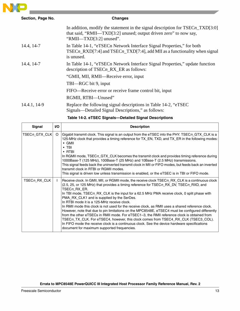
14.4.1, 14-9 Replace the following signal descriptions in Table 14-2, “eTSEC Signals—Detailed Signal Descriptions,” as follows:Table 14-2. eTSEC Signals—Detailed Signal Descriptions
Signal I/O Description
TSECn_GTX_CLK O Gigabit transmit clock. This signal is an output from the eTSEC into the PHY. TSECn_GTX_CLK is a 125-MHz clock that provides a timing reference for TX_EN, TXD, and TX_ER in the following modes: • GMII • TBI • RTBIIn RGMII mode, TSECn_GTX_CLK becomes the transmit clock and provides timing reference during 1000Base-T (125 MHz), 100Base-T (25 MHz) and 10Base-T (2.5 MHz) transmissions.This signal feeds back the uninverted transmit clock in MII or FIFO modes, but feeds back an inverted transmit clock in RTBI or RGMII modes.This signal is driven low unless transmission is enabled, or the eTSEC is in TBI or FIFO mode.
TSECn_RX_CLK I Receive clock. In GMII, MII, or RGMII mode, the receive clock TSECn_RX_CLK is a continuous clock (2.5, 25, or 125 MHz) that provides a timing reference for TSECn_RX_DV, TSECn_RXD, and TSECn_RX_ER.In TBI mode, TSECn_RX_CLK is the input for a 62.5 MHz PMA receive clock, 0 split phase with PMA_RX_CLK1 and is supplied by the SerDes.In RTBI mode it is a 125-MHz receive clock.In RMII mode this clock is not used for the receive clock, as RMII uses a shared reference clock.However, note that due to pin limitations on the MPC8548E, eTSEC4 must be configured differently from the other eTSECs in RMII mode. For eTSEC1–3, the RMII reference clock is obtained from TSECn_TX_CLK. For eTSEC4, however, this clock comes from TSEC4_RX_CLK (TSEC3_COL).In FIFO mode the receive clock is a continuous clock. See the device hardware specifications document for maximum supported frequencies.

Section, Page No. Changes
Errata to MPC8548E PowerQUICC III Integrated Host Processor Family Reference Manual, Rev. 2
14 Freescale Semiconductor
14.5, 14-12 Replace the third paragraph in the section with the following: “All accesses to and from the registers must be made as 32-bit accesses. There is no support for accesses of sizes other than 32 bits. Reads from unmapped register addresses return zero. Unless otherwise specified, the read value of reserved bits in mapped registers is not defined, and must not be assumed to be 0.”
14.5.1, 14-12 Add a row to Table 14-3 showing location of lossless flow control registers, as follows:
14.5.2/14-13 In Table 14-4, “Module Memory Map,” update reserved memory map range from “0x2_4034–0x2_404C” to” 0x2_4034–0x2_4054.”
TSECn_TX_EN O Transmit data valid. In GMII, MII, or RMII mode, if TSECn_TX_EN is asserted, the MAC is indicating that valid data is present on the GMII’s or the MII’s TSECn_TXD signals.In RGMII mode, TSECn_TX_EN becomes TX_CTL. TX_EN and TX_ERR are asserted on this signal on rising and falling edges of the TSECn_GTX_CLK, respectively. In TBI mode, TSECn_TX_EN represents TCG[8]. Together, with TCG[9] and TCG[7:0], they represent the 10-bit encoded symbol.In RTBI mode, TSECn_TX_EN represents TCG[4] on the rising edge and TCG[9] on the falling edge of TSECn_GTX_CLK, respectively. Together with TCG[3:0] and TCG[8:5], they represent the 10-bit encoded symbol.In FIFO mode TSECn_TX_EN is used to indicate valid data (GMII-style protocols) or forms part of the transmit control flags (encoded packet protocols).
TSECn_TX_CLK I Transmit clock in. In MII mode, TSECn_TX_CLK is a continuous clock (2.5 or 25 MHz) that provides a timing reference for the TSECn_TX_EN, TSECn_TXD, and TSECn_TX_ER signals.In GMII mode, this signal provides the 2.5 or 25 MHz timing reference during 10Base-T and 100Base-T and comes from the PHY. In 1000Base-T this clock is not used and TSECn_GTX_CLK (125 MHz) becomes the timing reference. The TSECn_GTX_CLK is generated in the eTSEC and provided to the PHY and the MAC. The TSECn_TX_CLK is generated in the PHY and provided to the MAC.In TBI mode, this signal is PMA receive clock 1 at 62.5 MHz, split phase with PMA_RX_CLK0, and is supplied by the SerDes.In RMII mode this signal is the reference clock shared between transmit and receive, and is supplied by the PHY.In FIFO mode the transmit clock is a continuous clock. See the device hardware specifications document for maximum supported frequencies.This signal is not used in the eTSEC RTBI or RGMII modes.
Table 14-3. Module Memory Map Summary
Address Offset Function
C00–C3F Lossless flow control registers
Table 14-2. eTSEC Signals—Detailed Signal Descriptions (continued)
Signal I/O Description

Section, Page No. Changes
Errata to MPC8548E PowerQUICC III Integrated Host Processor Family Reference Manual, Rev. 2
Freescale Semiconductor 15
14.5.2, 14-20 Add rows to Table 14-4 describing lossless flow control registers, as follows. Note that the references to section/page are valid for this document only and are subject to change in the next revision of the reference manual.
14.5.3.1.3, 14-24 Add sub-bullet to third primary bullet in IEVENT register description, defining special function interrupts as MSRO, MMWR, and MMRD.
14.5.3.1.3, 14-26 In Table 14-7, “IEVENT Field Descriptions,” change the second sentence of the CRL (bit 14) field description to say the following: “The frame is discarded without being transmitted and the queue halts (TSTAT[THLTn] set to 1).”
Table 14-4. Module Memory Map
eTSEC1 Offset
Name1
1 Registers denoted * are new to the enhanced TSEC and not supported by PowerQUICC III TSECs.
Access Reset Section/Page
eTSEC Lossless Flow Control Registers
0x2_4C00 RQPRM0*—Receive Queue Parameters register 0 R/W All zeros 14.5.3.11.1/15-155
0x2_4C04 RQPRM1*—Receive Queue Parameters register 1 R/W All zeros
0x2_4C08 RQPRM2*—Receive Queue Parameters register 2 R/W All zeros
0x2_4C0C RQPRM3*—Receive Queue Parameters register 3 R/W All zeros
0x2_4C10 RQPRM4*—Receive Queue Parameters register 4 R/W All zeros
0x2_4C14 RQPRM5*—Receive Queue Parameters register 5 R/W All zeros
0x2_4C18 RQPRM6*—Receive Queue Parameters register 6 R/W All zeros
0x2_4C1C RQPRM7*—Receive Queue Parameters register 7 R/W All zeros
0x2_4C20–0x2_4C40
Reserved — — —
0x2_4C44 RFBPTR0*—Last Free RxBD pointer for ring 0 R/W All zeros 14.5.3.11.2/15-156
0x2_4C48 Reserved — — —
0x2_4C4C RFBPTR1*—Last Free RxBD pointer for ring 1 R/W All zeros 14.5.3.11.2/15-156
0x2_4C50 Reserved — — —
0x2_4C54 RFBPTR2*—Last Free RxBD pointer for ring 2 R/W All zeros 14.5.3.11.2/15-156
0x2_4C58 Reserved — — —
0x2_4C5C RFBPTR3*—Last Free RxBD pointer for ring 3 R/W All zeros 14.5.3.11.2/15-156
0x2_4C60 Reserved — — —
0x2_4C64 RFBPTR4*—Last Free RxBD pointer for ring 4 R/W All zeros 14.5.3.11.2/15-156
0x2_4C68 Reserved — — —
0x2_4C6C RFBPTR5*—Last Free RxBD pointer for ring 5 R/W All zeros 14.5.3.11.2/15-156
0x2_4C70 Reserved — — —
0x2_4C74 RFBPTR6*—Last Free RxBD pointer for ring 6 R/W All zeros 14.5.3.11.2/15-156
0x2_4C78 Reserved — — —
0x2_4C7C RFBPTR7*—Last Free RxBD pointer for ring 7 R/W All zeros 14.5.3.11.2/15-156
Section, Page No. Changes
Errata to MPC8548E PowerQUICC III Integrated Host Processor Family Reference Manual, Rev. 2
16 Freescale Semiconductor
14.5.3.1.6, 14-31 In Table 14-10, “ECNTRL Field Descriptions,” update CLRCNT (bit 17) field description to read as follows:“Clear all statistics counters and carry registers.0 Allow MIB counters to continue to increment and keep any overflow
indicators.1 Reset all MIB counters and CAR1 and CAR2.This bit is self-resetting.”In addition, update AUTOZ (bit 18) field description to read as follows:“Automatically zero MIB counter values and carry registers.0 The user must write the addressed counter zero after a host read.1 The addressed counter value is automatically cleared to zero after a host read.This is a steady state signal and must be set prior to enabling the Ethernet controller and must not be changed without proper care.”
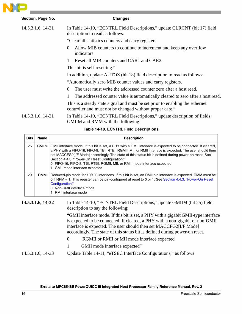
14.5.3.1.6, 14-31 In Table 14-10, “ECNTRL Field Descriptions,” update description of fields GMIIM and RMM with the following:
14.5.3.1.6, 14-32 In Table 14-10, “ECNTRL Field Descriptions,” update GMIIM (bit 25) field description to say the following:“GMII interface mode. If this bit is set, a PHY with a gigabit GMII-type interface is expected to be connected. If cleared, a PHY with a non-gigabit or non-GMII interface is expected. The user should then set MACCFG2[I/F Mode] accordingly. The state of this status bit is defined during power-on reset.0 RGMII or RMII or MII mode interface expected1 GMII mode interface expected”
14.5.3.1.6, 14-33 Update Table 14-11, “eTSEC Interface Configurations,” as follows:
Table 14-10. ECNTRL Field Descriptions
Bits Name Description
25 GMIIM GMII interface mode. If this bit is set, a PHY with a GMII interface is expected to be connected. If cleared, a PHY with a FIFO-16, FIFO-8, TBI, RTBI, RGMII, MII, or RMII interface is expected. The user should then set MACCFG2[I/F Mode] accordingly. The state of this status bit is defined during power-on reset. See Section 4.4.3, “Power-On Reset Configuration.”0 FIFO-16, FIFO-8, TBI, RTBI, RGMII, MII, or RMII mode interface expected1 GMII mode interface expected
29 RMM Reduced-pin mode for 10/100 interfaces. If this bit is set, an RMII pin interface is expected. RMM must be 0 if RPM = 1. This register can be pin-configured at reset to 0 or 1. See Section 4.4.3, “Power-On Reset Configuration.”0 Non-RMII interface mode1 RMII interface mode

Section, Page No. Changes
Errata to MPC8548E PowerQUICC III Integrated Host Processor Family Reference Manual, Rev. 2
Freescale Semiconductor 17
14.5.3.1.8, 14-35 In Table 14-13, “DMACTRL Field Descriptions,” change encodings for TOD field description, as follows:“0 eTSEC continues waiting for the TxBD ring 0 poll timer to expire.1 eTSEC immediately fetches a new TxBD from ring 0.”
14.5.3.1.8, 14-35 In Section 14.5.3.1.8, “ DMA Control Register (DMACTRL), update DMACTRL[16] to Reserved.
14.5.3.1.9, 14-36 Replace Figure 14-10, “TBIPA Register Definition,” with the following:
14.5.3.2, 14-36 Remove Section 14.5.3.2, “Receive and Transmit FIFO Control and Status Registers.”
14.5.3.3.1, 14-40 In Section 14.5.3.3.1, “Transmit Control Register (TCTRL), add the following note: “Except for TFC_PAUSE and THDF, which may be updated on-the-fly, no TCTRL field values should be upated without a GTSC (graceful transmit stop complete).”
Table 14-11. eTSEC Interface Configurations
Interface ModeECNTRL Field MACCFG2 Field
FIFM GMIIM TBIM RPM R100M RMM I/F Mode
FIFO 8-bits 1 0 0 1 0 0 —
FIFO 16-bits 1 0 0 0 0 0 —
TBI 1 Gbps 0 0 1 0 0 0 10
RTBI 1 Gbps 0 0 1 1 0 0 10
GMII 1 Gbps1
1 See MII 10/100 Mbps mode for GMII 10/100 Mbps ‘fall-back’ mode.
0 1 0 0 0 0 10
RGMII 1 Gbps 0 0 0 1 0 0 10
RGMII 100 Mbps 0 0 0 1 1 0 01
RGMII 10 Mbps 0 0 0 1 0 0 01
MII 10/100 Mbps 0 0 0 0 0 0 01
RMII 100 Mbps 0 0 0 0 1 1 01
RMII 10 Mbps 0 0 0 0 0 1 01
Offset eTSEC1:0x2_4030; eTSEC2:0x2_5030eTSEC3:0xB_6030; eTSEC4:0x2_7030
Access: Read/Write
0 26 27 31
R— TBIPA
W
Reset All zeros
Figure 14-10. TBIPA Register Definition

Section, Page No. Changes
Errata to MPC8548E PowerQUICC III Integrated Host Processor Family Reference Manual, Rev. 2
18 Freescale Semiconductor
14.5.3.3.1, 14-41 In Table 14-20 “TCTRL Field Description,” change TXSCHED field description for 01 state to read as follows: “Priority scheduling mode. Frames from enabled TxBD rings are serviced in ascending ring index order.”
14.5.3.3.2, 14-41 Replace second sentence of first paragraph, as follows:“The halt bit only has meaning for enabled rings.”

Section, Page No. Changes
Errata to MPC8548E PowerQUICC III Integrated Host Processor Family Reference Manual, Rev. 2
Freescale Semiconductor 19
14.5.3.3.2, 14-42 In Table 14-21, “TSTAT Field Descriptions,” replace descriptions of THLTn fields with the following:
Table 14-21. TSTAT Field Descriptions
Bits Name Description
0 THLT0 Transmit halt of ring 0. Set by the eTSEC if is no longer processing transmit frames from this TxBD ring, and DMA from this ring is disabled. To re-start transmission from this TxBD ring, this bit must be cleared by writing 1 to it. This bit is set only on a general error condition (as in IEVENT[TXE]), regardless of TQUEUE[EN0], or if no ready TxBDs can be fetched. DMACTRL[GTS] being set by the user does not cause this bit to be set.Software should examine the halted queue's buffer descriptors for repeatable error conditions before taking it out of the halt state. Failure to do so may cause an effective livelock, in which the error condition recurs and halts all queues again.
Repeatable error conditions which cause halt include:Bus error: • Invalid BD or data address • Uncorrectable error on BD or data read
TxBD programming errors: • Ready=1 and length=0
1 THLT1 Transmit halt of ring 1. Set by the eTSEC if is no longer processing transmit frames from this TxBD ring, and DMA from this ring is disabled. To re-start transmission from this TxBD ring, this bit must be cleared by writing 1 to it. This bit is set only on a general error condition (as in IEVENT[TXE]), regardless of TQUEUE[EN1], or if no ready TxBDs can be fetched.DMACTRL[GTS] being set by the user does not cause this bit to be set.Software should examine the halted queue's buffer descriptors for repeatable error conditions before taking it out of the halt state. Failure to do so may cause an effective livelock, in which the error condition recurs and halts all queues again.Repeatable error conditions which cause halt include:Bus error: Invalid BD or data addressUncorrectable error on BD or data readTxBD programming errors: • Ready=1 and length=0
2 THLT2 Transmit halt of ring 2. Set by the eTSEC if is no longer processing transmit frames from this TxBD ring, and DMA from this ring is disabled. To re-start transmission from this TxBD ring, this bit must be cleared by writing 1 to it. This bit is set only on a general error condition (as in IEVENT[TXE]), regardless of TQUEUE[EN2], or if no ready TxBDs can be fetched. DMACTRL[GTS] being set by the user does not cause this bit to be set.
Software should examine the halted queue's buffer descriptors for repeatable error conditions before taking it out of the halt state. Failure to do so may cause an effective livelock, in which the error condition recurs and halts all queues again.
Repeatable error conditions which cause halt include:Bus error: • Invalid BD or data addressUncorrectable error on BD or data readTxBD programming errors: • Ready=1 and length=0

Section, Page No. Changes
Errata to MPC8548E PowerQUICC III Integrated Host Processor Family Reference Manual, Rev. 2
20 Freescale Semiconductor
3 THLT3 Transmit halt of ring 3. Set by the eTSEC if is no longer processing transmit frames from this TxBD ring, and DMA from this ring is disabled. To re-start transmission from this TxBD ring, this bit must be cleared by writing 1 to it. This bit is set only on a general error condition (as in IEVENT[TXE]), regardless of TQUEUE[EN3], or if no ready TxBDs can be fetched. DMACTRL[GTS] being set by the user does not cause this bit to be set.Software should examine the halted queue's buffer descriptors for repeatable error conditions before taking it out of the halt state. Failure to do so may cause an effective livelock, in which the error condition recurs and halts all queues again.
Repeatable error conditions which cause halt include:Bus error: • Invalid BD or data address
Uncorrectable error on BD or data readTxBD programming errors: • Ready=1 and length=0
4 THLT4 Transmit halt of ring 4. Set by the eTSEC if is no longer processing transmit frames from this TxBD ring, and DMA from this ring is disabled. To re-start transmission from this TxBD ring, this bit must be cleared by writing 1 to it. This bit is set only on a general error condition (as in IEVENT[TXE]), regardless of TQUEUE[EN4], or if no ready TxBDs can be fetched. DMACTRL[GTS] being set by the user does not cause this bit to be set.Software should examine the halted queue's buffer descriptors for repeatable error conditions before taking it out of the halt state. Failure to do so may cause an effective livelock, in which the error condition recurs and halts all queues again.
Repeatable error conditions which cause halt include:Bus error: • Invalid BD or data address
Uncorrectable error on BD or data readTxBD programming errors: • Ready=1 and length=0
5 THLT5 Transmit halt of ring 5. Set by the eTSEC if is no longer processing transmit frames from this TxBD ring, and DMA from this ring is disabled. To re-start transmission from this TxBD ring, this bit must be cleared by writing 1 to it. This bit is set only on a general error condition (as in IEVENT[TXE]), regardless of TQUEUE[EN5], or if no ready TxBDs can be fetched. DMACTRL[GTS] being set by the user does not cause this bit to be set.Software should examine the halted queue's buffer descriptors for repeatable error conditions before taking it out of the halt state. Failure to do so may cause an effective livelock, in which the error condition recurs and halts all queues again.
Repeatable error conditions which cause halt include:Bus error: • Invalid BD or data address
Uncorrectable error on BD or data readTxBD programming errors: • Ready=1 and length=0
Table 14-21. TSTAT Field Descriptions (continued)
Bits Name Description

Section, Page No. Changes
Errata to MPC8548E PowerQUICC III Integrated Host Processor Family Reference Manual, Rev. 2
Freescale Semiconductor 21
14.5.3.3.3, 14-43 Replace fourth sentence of first paragraph with the following: “Frames with an Ethertype of 0x8808 will be dropped by the receiver.”
14.5.3.3.4, 14-44 In Table 14-23, “TXIC Field Descriptions,” add footnote to ICCS field description as follows:
6 THLT6 Transmit halt of ring 6. Set by the eTSEC if is no longer processing transmit frames from this TxBD ring, and DMA from this ring is disabled. To re-start transmission from this TxBD ring, this bit must be cleared by writing 1 to it. This bit is set only on a general error condition (as in IEVENT[TXE]), regardless of TQUEUE[EN6], or if no ready TxBDs can be fetched. DMACTRL[GTS] being set by the user does not cause this bit to be set.Software should examine the halted queue's buffer descriptors for repeatable error conditions before taking it out of the halt state. Failure to do so may cause an effective livelock, in which the error condition recurs and halts all queues again.
Repeatable error conditions which cause halt include:Bus error: • Invalid BD or data address
Uncorrectable error on BD or data readTxBD programming errors: • Ready=1 and length=0
7 THLT7 Transmit halt of ring 7. Set by the eTSEC if is no longer processing transmit frames from this TxBD ring, and DMA from this ring is disabled. To re-start transmission from this TxBD ring, this bit must be cleared by writing 1 to it. This bit is set only on a general error condition (as in IEVENT[TXE]), regardless of TQUEUE[EN7], or if no ready TxBDs can be fetched. DMACTRL[GTS] being set by the user does not cause this bit to be set.Software should examine the halted queue's buffer descriptors for repeatable error conditions before taking it out of the halt state. Failure to do so may cause an effective livelock, in which the error condition recurs and halts all queues again.
Repeatable error conditions which cause halt include:Bus error: • Invalid BD or data address
Uncorrectable error on BD or data readTxBD programming errors: • Ready=1 and length=0
21 TXF5 Transmit frame event occurred on ring 5. Set by the eTSEC if IEVENT[TXF] was set in relation to transmitting a frame from this ring.
22 TXF6 Transmit frame event occurred on ring 6. Set by the eTSEC if IEVENT[TXF] was set in relation to transmitting a frame from this ring.
23 TXF7 Transmit frame event occurred on ring 7. Set by the eTSEC if IEVENT[TXF] was set in relation to transmitting a frame from this ring.
Table 14-23. TXIC Field Descriptions
Bits Name Description
1 ICCS Interrupt coalescing timer clock source.0 The coalescing timer advances count every 64 eTSEC Tx interface clocks (TSECn_GTX_CLK).1 The coalescing timer advances count every 64 system clocks1. This mode is recommended for FIFO
operation.
1 The term ‘system clock’ refers to CCB clock/2.
Table 14-21. TSTAT Field Descriptions (continued)
Bits Name Description

Section, Page No. Changes
Errata to MPC8548E PowerQUICC III Integrated Host Processor Family Reference Manual, Rev. 2
22 Freescale Semiconductor
14.5.3.4.1, 14-50 Add field RCTRL[LFC] enabling lossless flow control (bit 17); add row to Table 14-31 describing field.
14.5.3.4.1, 14-51 In Table 14-31, “RCTRL Field Descriptions,” add the following note to RSF field description:“Note that frames less than or equal to 16B in length are always silently dropped.”
14.5.3.4.3, 14-54 In Table 14-33, “RXIC Field Descriptions,” add footnote to ICCS field description, as follows:
14.5.3.4.5, 14-56 Modify note in the second paragraph to read as follows:“Note: when the eTSEC is configured to receive frame through the FIFO packet interface, a value of BnCTL = 01 is not supported unless RCTRL[PRSFM]=1 and RCTRL[PRSDEP] is configured to parse L2 packets over the FIFO interface. Below is a list of arbitrary extraction requirements:
• Byte extraction level cannot exceed the parser depth: a value of BnCTL=10 requires RCTRL[PRSDEP]=1x and a value of BnCTL=11 requires RCTRL[PRSDEP]=11.
• For BnCTL = 01, BnOFFSET = 7 is not supported.• For values of BnCTL=10 or BnCTL=11, the controller extracts the defined bytes even if it does not
recognize the L3 or L4 header, respectively.• No L4 extraction is done if a packet is an IPV4 or IPV6 fragment frame.• If no extraction occurs due to BnOFFSET longer than frame data or it is an unsupported
BnOFFSET, the Bn extraction values are filled with zeros.”14.5.3.4.5, 14-57 Modify the RBIFX register description with respect to FIFO modes.
In addition, appended the following sentence to the 01 encoding of BnCTL field descriptions, as follows: “Values of B0OFFSET less than 8 are reserved in FIFO modes.”
Table 14-31. RCTRL Field Descriptions
Bits Name Description
17 LFC Lossless Flow Control. When set, the eTSEC will determine the number of free BDs (via RQPARMn[LEN] and RBTPTRn) in each active ring. Should the free BD count in an active ring drop below its setting for RQPARMn[FBTHR], the eTSEC will assert link layer flow control. For full-duplex ethernet connections, the eTSEC will emit a pause frame as if TCTRL[TFC_PAUSE] was set. For FIFO packet interface connections, the RFC signal will be asserted.0 Disabled. This is the default1 Enabled, calculate the free BDs in each active ring and assert link layer flow control if required.
Table 14-33. RXIC Field Descriptions
Bits Name Description
1 ICCS Interrupt coalescing timer clock source.0 The coalescing timer advances count every 64 eTSEC Rx interface clocks (TSECn_GTX_CLK).1 The coalescing timer advances count every 64 system clocks1. This mode is recommended for FIFO operation.
1 The term ‘system clock’ refers to CCB clock/2.

Section, Page No. Changes
Errata to MPC8548E PowerQUICC III Integrated Host Processor Family Reference Manual, Rev. 2
Freescale Semiconductor 23
In addition, change the definition of the 10 encoding of BnCTL to read, “Byte 0 is located in the received frame at offset B0OFFSET bytes from the byte after the last byte of the layer 2 header.” Also, change the definition of the 11 encoding of BnCTL to read: “Byte 0 is located in the received frame at offset B0OFFSET bytes from the byte after the last byte of the layer 3 header.”In addition, add notes that the offset cannot exceed the parser depth.
14.5.3.4, 14-58 Change the reset value from “All zeros” to “Undefined,” for the following registers:
• Receive Queue Filer Table Control Register (RQFCR)• Receive Queue Filer Table Property Register (RQFPR)
14.5.3.4.7. 14-58 In Table 14-37, “RQFCR Field Descriptions,” clarify AND (bit 24) field description to read as follows:“AND, in combination with CLE, REJ, and PID match, determines whether the filer will accept or reject a frame, defer evaluation until the next rule, exit a cluster, or skip a rule or set of rules.If CLE is zero:0 Match property[PID] against RQPROP. If matched, accept or reject frame
based on REJ. Otherwise skip to next rule.1 Match property[PID] against RQPROP. If matched, defer evaluation to next
rule. Otherwise, skip all rules up to and including the next rule with AND = 0. If the next rule with AND = 0 has CLE = 1, then also exit cluster.
If CLE is one:0 Match property[PID] against RQPROP. If matched, accept or reject frame
based on REJ. Otherwise, exit cluster.1 Match property[PID] against RQPROP. If matched, enter cluster. Otherwise,
skip all rules up to and including the next rule while CLE = 1 and AND = 0.”

Section, Page No. Changes
Errata to MPC8548E PowerQUICC III Integrated Host Processor Family Reference Manual, Rev. 2
24 Freescale Semiconductor
14.5.3.4.8, 14-61 In Table 14-38, “RQFPR Field Descriptions,” replace description of IPF and ETY with the following:
14.5.3.4.8, 14-62 In Table 14-38, “RQFPR Field Descriptions,” append the following parenthetical: “(Software should acknowledge the PIC=1 IP6 bit to distinguish proper alignment of the TOS field.)” to TOS field description (PID = 1010, bits 24–31).
14.5.3.6.1, 14-69 In Table 14-44, “MACCFG1 Field Descriptions,” add clarification to Rx Flow (bit 26) and Tx Flow (bit 27) field descriptions, as follows: “Must be 0 if MACCFG2[Full Duplex] = 0.”
14.5.3.6.2, 14-70 In Table 14-45, “MACCFG2 Field Descriptions,” replace description of Preamble Length field with the following:This field determines the length in bytes of the preamble field preceding each Ethernet start-of-frame delimiter byte. Values from 0x3 to 0xF are supported by the controller. The default value of 0x7 should not be altered in order to guarantee reliable operation with IEEE 802.3-compliant hardware.
Table 14-38. RQFPR Field Descriptions
PID1
1 PID is the property identifier field of the filer table control entry (see RQFCR[PID]) at the same index.
Bit Name Description
0001 20 IPF Set if a fragmented IPv4 or IPv6 header was encountered.See the descriptions of receive FCB fields IP and PRO in Section 14.6.4.3, “Receive Path Off-Load,” for more information on determining the status of received packets for which IPF is set.
0111 16–31 ETY Ethertype of next layer protocol, i.e., last ethertype if layer 2 headers nest. Defaults to 0xFFFF.
Using the filer to match ETY does not work in the case of PPPoE packets, because the PPPoE ethertype in the original packet, 0x8864, is always overwritten with the PPP protocol field. Thus, matches on ETY == 0x8864 always fail.
Instead, software should use PID=1 fields IP4 (ETY = 0x0021) and IP6 (ETY = 0x0057) to distinguish PPPoE session packets carrying IPv4 and IPv6 datagrams. Other PPP protocols are encoded in the ETY field, but many of them overlap with real ethertype definitions. Consult IANA and IEEE for possible ambiguities.
Packets with a value in the length/type field greater than 1500 and less than 1536 are treated as payload length. If the eTSEC is used in a network where there are packets carrying a type designation between 1500 and 1536 (note there are none currently publicly defined by IANA), then the S/W must confirm the parser and filer results by checking the type/length field after the packet has been written to memory to see if it falls in this range.Note that the eTSEC filer gets multiple packet attributes as a result of parsing the packet. The behavior of the eTSEC is that it will pull the innermost ethertype found in the packet; this means that in many supported protocols, it is impossible to create a filer rule that will match on the outer ethertype. There are four cases that need to be highlighted.1. The jumbo ethertype (0x8870)—In this case, the eTSEC assumes that the following header is
LLC/SNAP. LLC/SNAP has an associated ethertype, and the ETY field will be populated with that ethertype. This makes it impossible to file on jumbo frames.In this case, one can use arbitrary extracted bytes to pull the outermost Ethertype.
2. The PPPoE ethertype described above.3. The VLAN tag ethertype (0x8100)—In this case, one can use the PID1 VLN bit to indicate that the
packet had a VLAN tag.4. The MPLS tagged packets. In this case, one can use arbitrary extraction bytes to compare to the
actual ethertype if a filer rule is intending to file based on an MPLS label existence.

Section, Page No. Changes
Errata to MPC8548E PowerQUICC III Integrated Host Processor Family Reference Manual, Rev. 2
Freescale Semiconductor 25
In addition, replace bit settings of I/F Mode field description with the following:“00 Reserved01 MII/RMII/GMII/RGMII (10/100 Mbps) 10 GMII/RGMII/TBI/RTBI (1000 Mbps)11 Reserved”Also, update MACCFG2[PreAM RxEN] field description by appending the following sentence to the MACCFG2[PreAM RxEN] = 1 field description:“If the preamble is less than 7 bytes, 0’s are prepended to pad it to 7 bytes.”
14.5.3.6.2, 14-71 In Table 14-45, “MACCFG2 Field Descriptions,” update “Huge Frame” (bit 26) field description, as follows:
14.5.3.6.2, 14-71 In Table 14-45, “MACCFG2 Field Descriptions,” add the following sentence to description of PAD/CRC:“This bit must be set when in half-duplex mode (MACCFG2[Full Duplex] is cleared).”
14.5.3.6.4, 14-73 In Figure 14-44, “Half-Duplex Register Definition,” and Table 14-47, “HAFDUP Field Descriptions,” update the size of field “collision window” to be 26–31.
14.5.3.6.5, 14-74 In Table 14-48, “MAXFRM Descriptions,” modify the first paragraph of “Maximum Frame” (bits 16–31) field description, as follows:“This field is set to 0x0600 (1536 bytes) by default and always must be set to a value greater than or equal to 0x0040 (64 bytes), but not greater than 0x2580 (9600 bytes).It sets the maximum Ethernet frame size in both the transmit and
Table 14-45. MACCFG2 Field Descriptions
Bits Name Description
26 HugeFrame
Huge frame enable. This bit is cleared by default.0 Limit the length of frames received to less than or equal to the maximum frame length value
(MAXFRM[Maximum Frame]) and limit the length of frames transmitted to less than the maximum frame length. See Section 14.6.6, “Buffer Descriptors,” for further details of buffer descriptor bit updating.
Frame type Frame lengthPacket
truncationBuffer descriptor
updated
Receive or transmit > maximum frame length yes yes
Receive = maximum frame length no no
Transmit = maximum frame length no yes
Receive or transmit < maximum frame length no no
1 Frames are transmitted and received regardless of their relationship to the maximum frame length.Note that if Huge Frame is cleared, the user must ensure that adequate buffer space is allocated for
received frames. See Section 14.5.3.6.5, “Maximum Frame Length Register (MAXFRM),” for further information.

Section, Page No. Changes
Errata to MPC8548E PowerQUICC III Integrated Host Processor Family Reference Manual, Rev. 2
26 Freescale Semiconductor
receive directions. (Refer to MACCFG2[Huge Frame].) It does not affect the size of packets sent or received via the FIFO packet interface.
14.5.6.3.9, 14-76 Update Figure 14-49, “MII Mgmt Control Register Definition,” to be write-only.14.5.3.7, 14-81 Add the following note before the TR64 register:
NOTEThe transmit and receive frame counters (TR64, TR127, TR 255, TR511, TR1K, TRMAX, and TRMGV) do not increment for aborted frames (collision retry limit exceeded, late collision, underrun, EBERR, TxFIFO data error, frame truncated due to exceeding MAXFRM, or excessive deferral).
14.5.3.7, 14-81 Add the following notes to end of section:
NOTERMON counters do not comprehend custom VLAN tagged frames. Affected counters include TRMGV, RMCA, RBCA, RXCF, RXPF, RXUO, RALN, RFLR, ROVR, RJBR, TMCA, TBCA, TXPF, TXCF. Specifically, custom VLAN tagged frames are not afforded the ability to be greater than 1518, as compared to the IEEE standard tagged frames.
NOTEThe transmit and receive frame counters (TR64, TR127, TR 255, TR511, TR1K, TRMAX, and TRMGV) do not increment for aborted frames (collision retry limit exceeded, late collision, underrurn, EBERR, TxFIFO data error, frame truncated due to exceeding MAXFRM, or excessive deferral).
14.5.3.7.17, 14-89 In Table 14-76, “RFLR Field Descriptions,” add the following text to the RFLR (bits 16–31) field description: “Frames tagged with a single VLAN tag are checked for valid length based on bytes 17–18 (rather than 13–14). Frames tagged (stacked) with multiple VLAN tags are not checked for valid length.”
14.5.3.7.25, 14-93 In Figure 14-81, “Transmit Byte Counter Register Definition,” fortify TBYT field description, as follows:Second sentence formerly read: “This count does not include preamble/SFD or jam bytes.”Now reads: “This count does not include preamble/SFD or jam bytes, except for half-duplex flow control (back-pressure triggered by TCTRL[THDF]=1). For THDF, the sum total of ‘phantom’ preamble bytes transmitted for flow control purposes is included in the TBYT increment value of the next frame to be transmitted, up to 65,535 bytes of frame and phantom preamble.”
Section, Page No. Changes
Errata to MPC8548E PowerQUICC III Integrated Host Processor Family Reference Manual, Rev. 2
Freescale Semiconductor 27
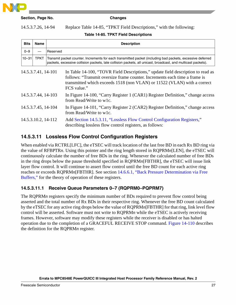
14.5.3.7.26, 14-94 Replace Table 14-85, “TPKT Field Descriptions,” with the following:
14.5.3.7.41, 14-101 In Table 14-100, “TOVR Field Descriptions,” update field description to read as follows: “Transmit oversize frame counter. Increments each time a frame is transmitted which exceeds 1518 (non VLAN) or 11522 (VLAN) with a correct FCS value.”
14.5.3.7.44, 14-103 In Figure 14-100, “Carry Register 1 (CAR1) Register Definition,” change access from Read/Write to w1c.
14.5.3.7.45, 14-104 In Figure 14-101, “Carry Register 2 (CAR2) Register Definition,” change access from Read/Write to w1c.
14.5.3.10.2, 14-112 Add Section 14.5.3.11, “Lossless Flow Control Configuration Registers,” describing lossless flow control registers, as follows:
14.5.3.11 Lossless Flow Control Configuration Registers
When enabled via RCTRL[LFC], the eTSEC will track location of the last free BD in each Rx BD ring via the value of RFBPTRn. Using this pointer and the ring length stored in RQPRMn[LEN], the eTSEC will continuously calculate the number of free BDs in the ring. Whenever the calculated number of free BDs in the ring drops below the pause threshold specified in RQPRMn[FBTHR], the eTSEC will issue link layer flow control. It will continue to assert flow control until the free BD count for each active ring reaches or exceeds RQPRMn[FBTHR]. See section 14.6.6.1, “Back Pressure Determination via Free Buffers,” for the theory of operation of these registers.
14.5.3.11.1 Receive Queue Parameters 0–7 (RQPRM0–PQPRM7)
The RQPRMn registers specify the minimum number of BDs required to prevent flow control being asserted and the total number of Rx BDs in their respective ring. Whenever the free BD count calculated by the eTSEC for any active ring drops below the value of RQPRMn[FBTHR] for that ring, link level flow control will be asserted. Software must not write to RQPRMn while the eTSEC is actively receiving frames. However, software may modify these registers while the receiver is disabled or has halted operation due to the completion of a GRACEFUL RECEIVE STOP command. Figure 14-110 describes the definition for the RQPRMn register.
Table 14-85. TPKT Field Descriptions
Bits Name Description
0–9 — Reserved
10–31 TPKT Transmit packet counter. Increments for each transmitted packet (including bad packets, excessive deferred packets, excessive collision packets, late collision packets, all unicast, broadcast, and multicast packets).
Section, Page No. Changes
Errata to MPC8548E PowerQUICC III Integrated Host Processor Family Reference Manual, Rev. 2
28 Freescale Semiconductor
This table describes the fields of the RQPRM register.
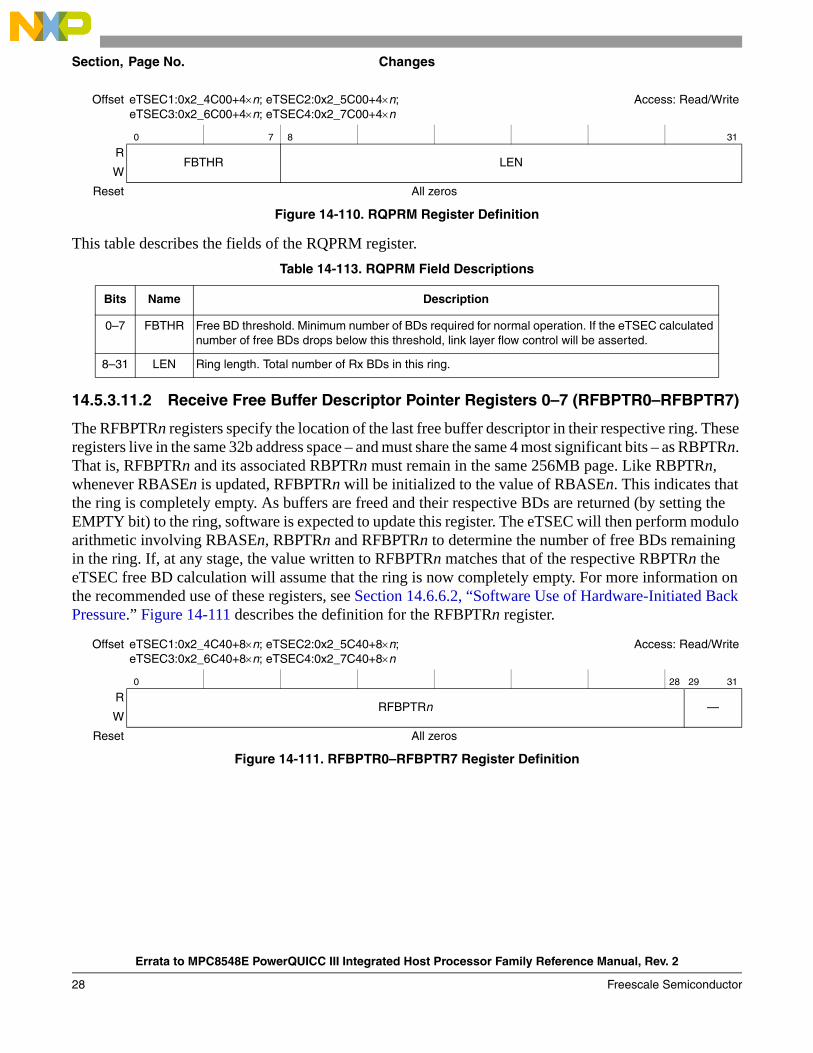
14.5.3.11.2 Receive Free Buffer Descriptor Pointer Registers 0–7 (RFBPTR0–RFBPTR7)
The RFBPTRn registers specify the location of the last free buffer descriptor in their respective ring. These registers live in the same 32b address space – and must share the same 4 most significant bits – as RBPTRn. That is, RFBPTRn and its associated RBPTRn must remain in the same 256MB page. Like RBPTRn, whenever RBASEn is updated, RFBPTRn will be initialized to the value of RBASEn. This indicates that the ring is completely empty. As buffers are freed and their respective BDs are returned (by setting the EMPTY bit) to the ring, software is expected to update this register. The eTSEC will then perform modulo arithmetic involving RBASEn, RBPTRn and RFBPTRn to determine the number of free BDs remaining in the ring. If, at any stage, the value written to RFBPTRn matches that of the respective RBPTRn the eTSEC free BD calculation will assume that the ring is now completely empty. For more information on the recommended use of these registers, see Section 14.6.6.2, “Software Use of Hardware-Initiated Back Pressure.” Figure 14-111 describes the definition for the RFBPTRn register.
Offset eTSEC1:0x2_4C00+4×n; eTSEC2:0x2_5C00+4×n;eTSEC3:0x2_6C00+4×n; eTSEC4:0x2_7C00+4×n
Access: Read/Write
0 7 8 31
RFBTHR LEN
W
Reset All zeros
Figure 14-110. RQPRM Register Definition
Table 14-113. RQPRM Field Descriptions
Bits Name Description
0–7 FBTHR Free BD threshold. Minimum number of BDs required for normal operation. If the eTSEC calculated number of free BDs drops below this threshold, link layer flow control will be asserted.
8–31 LEN Ring length. Total number of Rx BDs in this ring.
Offset eTSEC1:0x2_4C40+8×n; eTSEC2:0x2_5C40+8×n;eTSEC3:0x2_6C40+8×n; eTSEC4:0x2_7C40+8×n
Access: Read/Write
0 28 29 31
RRFBPTRn —
W
Reset All zeros
Figure 14-111. RFBPTR0–RFBPTR7 Register Definition

Section, Page No. Changes
Errata to MPC8548E PowerQUICC III Integrated Host Processor Family Reference Manual, Rev. 2
Freescale Semiconductor 29
Table 14-114 describes the fields of the RFBPTRn registers.
14.5.3.10.2, 14-113 In Table 14-112, “ATTRELI Field Descriptions,” replace EI (bits 18–25) field description with the following: “Extracted index. Points to the first byte, as a multiple of 64 bytes, within the receive frame as sent to memory from which to begin extracting data.”
14.5.3.10.2, 14-113 In Figure 14-109, “ATTRELI Register Definition,” and Table 14-112, “ATTRELI Field Descriptions,” change size of AEI field. The updated register definition and field description appear as follows:
14.5.4.3.10, 14-124 In Table 14-124, “TBICON Field Descriptions,” modify “Clock Select” field description to read as follows:“Clock select. This bit selects how the on-chip TBI PHY is clocked.This bit is cleared by default.0 The TBI PHY is clocked by dual split-phase 62.5 MHz receive clocks. These
external signals must be provided via TBI receive clock 0 (TSECn_RX_CLK) and TBI receive clock 1 (TSECn_TX_CLK).
1 The TBI PHY is clocked by a single 125 MHz receive clock. This single clock must be provided via the TBI receive clock 0 (TSECn_RX_CLK) external signal.”
Table 14-114. RFBPTR0–RFBPTR7 Field Descriptions
Bits Name Description
0–28 RFBPTR Pointer to the last free BD in RxBD Ring n. When RBASEn is updated, eTSEC initializes RFBPTRn to the value in the corresponding RBASEn. Software may update this register at any time to inform the eTSEC the location of the last free BD in the ring. Note that the 3 least-significant bits of this register are read only and zero.
29–31 — Reserved.
Offset eTSEC1:0x2_4BFC; eTSEC2:0x2_5BFC;eTSEC3:0x2_6BFC; eTSEC4:0x2_7BFC
Access: Read/Write
0 1 2 12 13 17 18 25 26 31
R— EL — EI —
W
Reset All zeros
Figure 14-109. ATTRELI Register Definition
Table 14-112. ATTRELI Field Descriptions
Bits Name Description
18–25 EI Extracted index. Points to the first byte, as a multiple of 64 bytes, within the receive frame from which to begin extracting data.

Section, Page No. Changes
Errata to MPC8548E PowerQUICC III Integrated Host Processor Family Reference Manual, Rev. 2
30 Freescale Semiconductor
14.6.1, 14-126 Change the wording of third paragraph to reference overriding the protocol interface voltage of a TBI interface to 2.5 V (from the specified 3.3 V) rather than referencing GMII, because TBI is the only protocol that supports such voltage override.
14.6.1, 14-126 Replace third paragraph with the following:“If a user wishes to override the voltage dictated by the protocol—like running TBI at 2.5 V instead of the specified 3.3 V—the registers that enable the user to do this are TSEC12IOOVCR (see Section 20.4.1.26, “eTSEC1 and eTSEC2 I/O Overdrive Control Register (TSEC12IOOVCR)”) and TSEC23IOOVCR (see Section 20.4.1.27, “eTSEC3 and eTSEC4 I/O Overdrive Control Register (TSEC34IOOVCR)).”
14.6.1.3.1.2, 14-143 In Table 14-134, “Steps for Minimum Register Intialization,” update the steps for register initialization by swapping step 1 and step 2 to the following:1. Initialize MACCFG22. Set and clear MACCFG1[Soft_Reset]
14.6.2, 14-136 Replace first bullet under “The following restrictions apply in any of the FIFO modes” with the following:
• Transferred packets must by no more than 9600 bytes in length.• If RCTRL[PRSFM]=0, received packets must be a minimum of 10 bytes.
If RCTRL[PRSFM]=1, received packets must be a minimum of 14 bytes.• Transmitted packets with L2 headers must be a minimum of 14 bytes.
Transmitted packets without L2 headers must be a minimum of 10 bytes.14.6.1.7, 14-133 Add note to Table 14-126, “GMII, MII, and RMII Signals Multiplexing,”
clarifying that RX_ER does not exist on eTSEC4.14.6.3.2, 14-144 Update step 3 to appear as follows:
“3. Set SOFT_RESET bit in MACCFG1 register (Note that SOFT_RESET must remain set for at least 3–10 TX clocks before proceeding.)
14.6.3.8, 14-153 Replace last sentence of section with the following:“Only frames addressed specifically to the MAC’s station address or a valid multicast or broadcast address can be examined for the Magic Packet sequence.”
14.3.6.10, 14-154 Clarify three sub-bullets under first primary bullet, noting that anything other than RXB, RXF, TXB, or TXF are classified as “error, diagnostic, or special interrupts.”
14.6.3.9, 14-154 Update second sentence of third paragraph to say, “The controller completes any frame in progress before stopping transmission and does not commence counting the pause time until transmit is idle.”
14.6.3.11, 14-157 Add the following to the bulleted list after the first paragraph:• All BDs for any multiple-BD frame reside in the same cache line.• TCP/UDP and IP Checksum generation are disabled in each frame’s TxFCB,
or in TCTRL, or frames are limited to 1200 bytes in length.

Section, Page No. Changes
Errata to MPC8548E PowerQUICC III Integrated Host Processor Family Reference Manual, Rev. 2
Freescale Semiconductor 31
14.6.3.13, 14-158 In Table 14-142, “Reception Errors,” add the following note to parser error description:“Note: Any values in the length/type field between 1500 and 1536 is treated as a length, however, only illegal packets exist with this length/type since these are not valid lengths and not valid types. These are treated by the MAC logic as out of range.Software must confirm the parser and filer results by checking the type/length field after the packet has been written to memory to see if it falls in this range.”
14.6.4.3, 14-163 In Table 14-144, “Rx Frame Control Block Descriptions,” replace descriptions of IP and PRO with the following:
14.6.5, 14-163 Add Section 14.6.5.1, “Receive Parser,” as follows:
14.6.5.1 Receive Parser
The receive parser parses the incoming frame data and generates filer properties and frame control block (FCB). The receive parser composes of the Ethernet header parser and L3/L4 parser.
The Ethernet header parser parses only L2 (ethertype) headers. It is enabled by RCTRL[PRSDEP] != 0. It has the following key features:
• Extraction of 48-bit MAC destination and source addresses
Table 14-144. Rx Frame Control Block Descriptions
Bytes Bits Name Description
0–1 1 IP IP header found at layer 3. RCTRL[PRSDEP] must be set to 10 or 11 in order to enable IP discovery. See also IP6 bit of FCB.0 No layer 3 header recognized.1 An IP header was recognized at layer 3; the IANA protocol identifier for the next header can be found
in PRO; see PRO for more information.
If S/W is relying on the RxFCB for the parse results, any RxFCB[IP] bits set with the corresponding RxFCB[PRO] = 0xFF indicates a fragmented packet (or that this packet had a back-to-back IPv6 routing extension header. Additionally, RQFPR[IPF] (see Section 14.5.3.4.8, “Receive Queue Filer Table Property Register (RQFPR)”) indicates that the packet was fragmented.
2–3 8–15 PRO If IP = 1, PRO is set as follows: • PRO=0xFF for a fragment header or a back to back route header • PRO=0xnn for an unrecognized header, where nn is the next protocol field • PRO=(TCP/UDP header), as defined in the IANA specification, if TCP or UDP header is found
If IP = 0, PRO is undefined.
Note that the eTSEC parser logic stops further parsing when encountering an IP datagram that has indicated that it has fragmented the upper layer protocol. This in general means that there is likely no layer 4 header following the IP header and extension headers. eTSEC leaves the RxFCB[PRO] and RQFPR[L4P] fields 0xFF in this case, which usually means that there was no IP header seen. In this case RxFCB[IP] and optionally RxFCB[IP6] will be set. IP header checksumming will operate and perform as intended. Most of the time, the eTSEC will update the RxFCB[PRO] field and RQFPR[L4P] fields with whatever value was found in the protocol field of the IP header. See Section 14.5.3.4.8, “Receive Queue Filer Table Property Register (RQFPR),” for a description of RQFPR.
Section, Page No. Changes
Errata to MPC8548E PowerQUICC III Integrated Host Processor Family Reference Manual, Rev. 2
32 Freescale Semiconductor
• Extraction and recognition of the first 2-byte ethertype field• Extraction and recognition of the final 2-byte ethertype field• Extraction of 2-byte VLAN control field• Walk through MPLS stack and find layer 3 protocol• Walk through VLAN stack and find layer 3 protocol• Recognition of the following ethertypes for inner layer parsing
— LLC and SNAP header— JUMBO and SNAP header— IPV4 — IPV6— VLAN— MPLSU/MPLSM— PPPOES
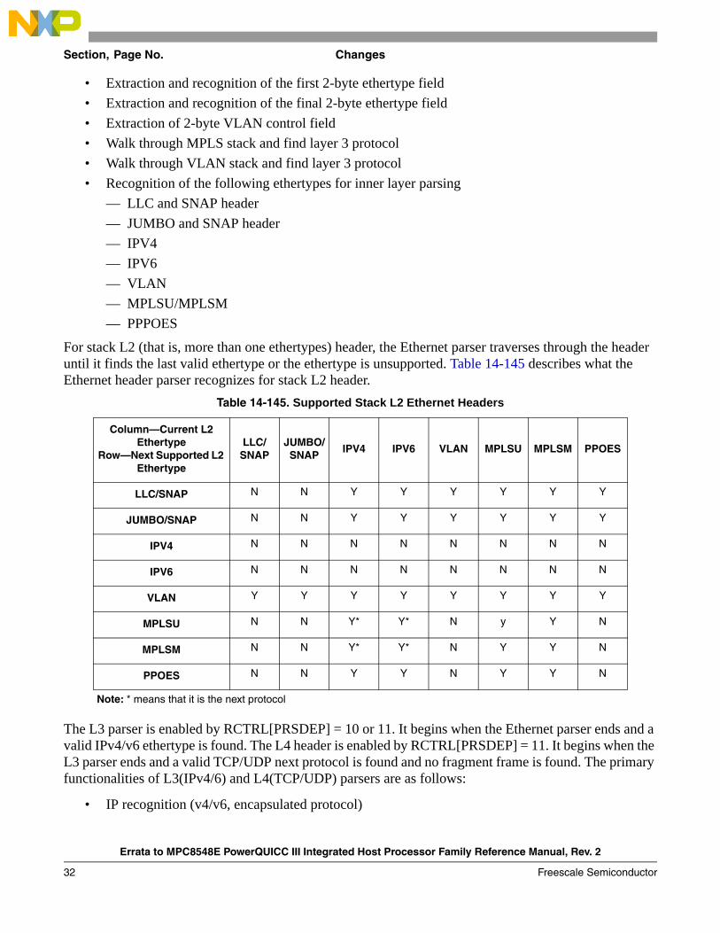
For stack L2 (that is, more than one ethertypes) header, the Ethernet parser traverses through the header until it finds the last valid ethertype or the ethertype is unsupported. Table 14-145 describes what the Ethernet header parser recognizes for stack L2 header.
The L3 parser is enabled by RCTRL[PRSDEP] = 10 or 11. It begins when the Ethernet parser ends and a valid IPv4/v6 ethertype is found. The L4 header is enabled by RCTRL[PRSDEP] = 11. It begins when the L3 parser ends and a valid TCP/UDP next protocol is found and no fragment frame is found. The primary functionalities of L3(IPv4/6) and L4(TCP/UDP) parsers are as follows:
• IP recognition (v4/v6, encapsulated protocol)
Table 14-145. Supported Stack L2 Ethernet Headers
Column—Current L2 Ethertype
Row—Next Supported L2 Ethertype
LLC/SNAP
JUMBO/SNAP
IPV4 IPV6 VLAN MPLSU MPLSM PPOES
LLC/SNAP N N Y Y Y Y Y Y
JUMBO/SNAP N N Y Y Y Y Y Y
IPV4 N N N N N N N N
IPV6 N N N N N N N N
VLAN Y Y Y Y Y Y Y Y
MPLSU N N Y* Y* N y Y N
MPLSM N N Y* Y* N Y Y N
PPOES N N Y Y N Y Y N
Note: * means that it is the next protocol
Section, Page No. Changes
Errata to MPC8548E PowerQUICC III Integrated Host Processor Family Reference Manual, Rev. 2
Freescale Semiconductor 33
• IP header checksum verification• IPv4/6 over IPv4/6 (tunneling)—parse headers and find layer 4 protocol• IP layer 4 protocol/next header extraction• Stop parsing on unrecognized next header/protocol• IPv4 support
— IPv4 source and destination addresses— 8-bit IPv4 type of service— IP layer 4 protocol / next header support
– IPV4– IPV4 Fragment. Parser stops after a fragment is found– TCP/UDP
• IPv6 support— The first 4 bytes of the IPv6 source address extraction— The first 4 bytes of the IPv6 destination address extraction— IPv6 source address hash for pseudo header calculation— IPv6 destination address hash for pseudo header calculation— 8-bit IPv6 traffic class field extraction— Payload length field extraction— IP layer 4 protocol/next header support
– IPV6– IPV6 fragment. Parser stops after a fragment is found– IPV6 route – IPV6 hop/destination– TCP/UDP
• L4 (TCP/UDP) support
– Extraction of 16-bit source port number extraction
– Extraction of 16-bit destination port number extraction
– TCP checksum calculation (including pseudo header)
– UDP checksum calculation if the checksum field is not zero (including pseudo header)
14.5.3.6.1, 14-168 Data length is the number of octets written by the eTSEC into this BD’s data buffer if L is cleared (the value is equal to MRBLR), or, if L is set, the length of the frame including CRC, FCB (if RCTRL[PRSDEP > 00), preamble (if MACCFG2[PreAmRxEn]=1), and any padding (RCTRL[PAL]).”In Table 14-44, “MACCFG1 Field Descriptions,” add the following note to Tx_Flow and Rx_Flow:“Note: Should not be set when operating in Half-Duplex mode”

Section, Page No. Changes
Errata to MPC8548E PowerQUICC III Integrated Host Processor Family Reference Manual, Rev. 2
34 Freescale Semiconductor
14.5.3.6.1, 14-69 In Table 14-44, “MACCFG1 Field Descriptions,” add the following note for MACCFG1[Loop Back] bit: “MAC_level loopback is not supported in 10-bit mode.”
14.5.3.6.3, 14-72 Replace Section 14.5.3.6.3, “Inter-Packet Gap/Inter-Frame Gap Register (IPGIFG),” with the following:
14.5.3.6.3 Inter-Packet Gap/Inter-Frame Gap Register (IPGIFG)
The IPGIFG register is written by the user. This figure describes the definition for IPGIFG.
This table describes the fields of the IPGIFG register.
Offset eTSEC1:0x2_4508; eTSEC2:0x2_5508;eTSEC3:0x2_6508; eTSEC4:0x2_7508
Access: Read/Write
0 1 7 8 9 15 16 23 24 25 31
R— IPGR1 — IPGR2
Minimum IFGEnforcement
— IPGR3W
Reset 0 1 0 0 0 0 0 0 0 1 1 0 0 0 0 0 0 1 0 1 0 0 0 0 0 1 1 0 0 0 0 0
Figure 14-43. IPGIFG Register Definition
Table 14-64. IPGIFG Field Descriptions
Bits Name Description
0 — Reserved
1–7 IPGR1 Non_Back_to_Back_Interpacket_Gap_Part_1.This is a programmable field representing the optional carrier sense window referenced in IEEE 802.3/4.2.3.2.1 ‘carrier deference’. If carrier is detected during the timing of IPGR1, the MAC defers to carrier. If, however, carrier becomes active after IPGR1, the MAC continues timing IPGR2 and transmits, knowingly causing a collision, thus ensuring fair access to medium. Its range of values is 0x00 to IPGR2.Its default is 0x40 (64d) which follows the two-thirds/one-third guideline.Note: To correctly follow the two-thirds/one-third guideline, program IPGR1 to 0x5C,
assuming that IPGR2 is the default 0x60 (96d). If the IPGR2 value is anything other than default use the following equation to calculate IPGR1= [(2/3 X IPGR2) + 28].
8 — Reserved
9–15 IPGR2 Non_Back_to_Back_Interpacket_Gap_Part_2.This is a programmable field representing the non-back-to-back inter-packet-gap in bits. Its default is 0x60 (96d), which represents the minimum IPG of 96 bits.
16–23 Minimum IFGEnforcement
This is a programmable field representing the minimum number of bits of IFG to enforce between frames. A frame is dropped whose IFG is less than that programmed. The default setting of 0x50 (80d) represents half of the nominal minimum IFG which is 160 bits.
24 — Reserved
25–31 IPGR3 Back_to_Back_Interpacket_Gap.This is a programmable field representing the IPG between back-to-back packets. This is the IPG parameter used exclusively in full-duplex mode and in half-duplex mode if two transmit packets are sent back-to-back. Set this field to the number of bits of IPG desired. The default setting of 0x60 (96d) represents the minimum IPG of 96 bits.

Section, Page No. Changes
Errata to MPC8548E PowerQUICC III Integrated Host Processor Family Reference Manual, Rev. 2
Freescale Semiconductor 35
14.5.4.3, 14-115 In Section 14.5.4.3, “TBI MII Set Register Descriptions,” rename AN Advertisement Register (ANA) and AN Link Partner Base Page Ability Register (ANLPBPA) to AN Advertisement Register (ANA) for 1000Base-X Auto-Negotiation and AN Link Partner Base Page Ability Register (ANLPBPA) for 1000Base-X Auto-Negotiation.
14.6.5.1.1, 14-164 After the second paragraph in Section 14.6.5.1.1, “Filing Rules,” add the following:
“The equation to calculate the maximum rules is MaxRules = (sysclk/phyclk) × 2 × (TF + IFG) where:• sysclk = eTSEC clock frequency• phyclk = clock frequency of physical interface• TF = number of PHY clocks between start of one frame and when the parser is finished with
parsing the frame.• IFG = interframe gap”
14.6.5.2.1, 14-169 Replace Section 14.6.5.2.1, “Priority-Based Queuing (PBQ),” with the following:
“PBQ is the simplest scheduler decision policy. The enabled TxBD rings are assigned a priority value based on their index. Rings with a lower index have precedence over rings with higher indices, with priority assessed on a frame-by-frame basis. For example, frames in TxBD ring 0 have higher priority than frames in TxBD ring 1, and frames in TxBD ring 1 have higher priority than frames in TxBD ring 2, and so on.
The scheduling decision is then achieved as follows: loop
# start or S/W clear of TSATnring = 0;while ring <= 7 loopif enabled(ring) and not ring_empty(ring) then
transmit_frame(ring);ring = 0;
elsering = ring + 1;
endifendloop
endloop
14.6.6, 14-171 Remove last sentence of first paragraph. This change applies to the last revision of this document—this section has never appeared in the published reference manual.
14.6.6, 14-171 Add Section 14.6.6, “Lossless Flow Control,” describing lossless flow control, as follows:
14.6.6 Lossless Flow Control
The eTSEC DMA subsystem is designed to be able to support simultaneous receive and transmit traffic at gigabit line rates. If the host memory has sufficient bandwidth to support such line rates, then the principle

Section, Page No. Changes
Errata to MPC8548E PowerQUICC III Integrated Host Processor Family Reference Manual, Rev. 2
36 Freescale Semiconductor
cause of overflow on receive traffic will be due to a lack of Rx BDs. Thus, the long term receive throughput will be determined by the rate at which software can process receive traffic. If a user desires to prevent dropped packets, they can inform the far-end link to stop transmission while the software processing catches up with the backlog.
To avoid overflow in the latter case, back pressure must be applied to the far-end transmitter before the Rx descriptor controller encounters a non-empty BD and halts with a BSY error. As there is lag between application of back-pressure and response of the far-end, the pause request must be issued while there are still BDs free in the ring. In the traditional eTSEC descriptor ring programming model, there is no way for hardware to know how many free BDs are available, so software must initiate any pause requests required during operation. If software is backlogged, the request may be not be issued in time to prevent BSY errors. To allow the eTSEC to generate the pause request automatically, additional information (a pointer the last free BD and ring length) is required.
14.6.6.1 Back Pressure Determination via Free Buffers
Ultimately, the rate of data reception is determined by how quickly software can release buffers back into the receive ring(s). Each time a buffer is freed, the associated BD has its empty bit set and hardware is free to consume both. Thus the number of free BDs in a given Rx ring indicates how close hardware is to the end of that ring. To prevent data loss, back pressure should be applied when the number of free BDs drops below some critical level. The number of BDs that can be consumed by an incoming packet stream while back-pressure takes effect is determined by several factors, such as: receive traffic profile, transmit traffic profile, Rx buffer size, physical transmission time between eTSEC and far-end device and intra-device latency. Theoretically, the worst case will be:
This case comes about when:• The eTSEC has just started transmitting a large frame and thus cannot send out a pause frame• Upon reception of the pause request the far-end has just started transmission of a large frame• The eTSEC receives a burst of short frames with minimum inter-frame-gap (96bit times for
ethernet)
Once the user has determined the worst case scenario for their application, they program the required free BD threshold into the eTSEC (via RQPRM[PBTHR]). Since different BD rings may have different sizes and expected packet arrival rates, a separate threshold is provided for each active ring. It is recommended that a threshold of at least three BDs is the practical minimum for gigabit ethernet links.
For the Rx descriptor controller to determine the number of free BDs remaining in the ring, it needs to know the following:
1. The location of the current BD being used by hardware2. The location of the last BD that was released (freed) by software3. The length of the Rx BD ring.
FreeBDsRequired MaxFrameSizeMinFrameSize IFG+----------------------------------------------------------- MaxFrameSize
RxBufferSize-------------------------------------------- LinkDelay+ +=

Section, Page No. Changes
Errata to MPC8548E PowerQUICC III Integrated Host Processor Family Reference Manual, Rev. 2
Freescale Semiconductor 37
For each active ring, the current BD pointer (RBPTRn) is maintained by the eTSEC. Software will know both the size of the Rx ring and the location of the last freed BD. By providing the eTSEC with those values (via RQPRM[LEN] and RFBPTR respectively) the eTSEC will always know how many receive buffers are available to be consumed by incoming data.
The number of guaranteed free BDs in the ring is then determined by:
When RFBPTRn < RBPTRn
When RFBPTRn > RBPTRn
When RBPTRn = RFBPTRn the number of free BDs in the ring is either one (since RFBPTRn points to a free BD) or equal to the ring length. Since the BD pointed to by RBPTRn may be either in use or about to be used, it is not considered in the free BD count. To resolve the case where the two pointers collide, the following logic applies:
If RBASEn was updated and thus initializes both RBPTRn and RFBPTRn, the ring is deemed empty.
If RFBPTRn is updated by a software write and matches RBPTRn, the ring is deemed empty.
If HW updates RBPTRn and the result matches RFBPTRn, the ring is deemed to have one BD remaining. Upon writing this BD back to memory (indicating the buffer is occupied) the ring is deemed to be full.
Important. There is a possibility that if software is severely backlogged in updating RFBPTRn, the hardware could wrap around the ring entirely, consume exactly the remaining number of BDs and not halt with a BSY error. If software then increments RFBPTRn to the next address (thereby equalling RBPTRn), the hardware will assume the ring is now empty (when in fact there is only a single BD freed up). This will result in the hardware failing to maintain back pressure on the far end. Upon software incrementing RFBPTRn a subsequent time, the wrap condition will be successfully detected and hardware will recognize a nearly full ring (rather than a nearly empty one). Since software can increment RFBPTRn by any amount, it is not possible for hardware to determine in this case whether the user has cleared the entire ring or just one BD. Users can eliminate the possibility of this condition occurring by ensuring that RFBPTRn is incremented by at least two BDs each time (i.e. clear at least two buffers whenever the RxBD unload routine is called).
Once the eTSEC determines that this threshold has been reached, back pressure will be applied accordingly. The type of back pressure that is applied will vary according to the physical interface that is used.
• Half duplex Ethernet: No support in this mode.• Full duplex Ethernet: An IEEE 802.3 PAUSE frame (see Section 14.6.3.9, “Flow Control”) will
be issued as if the TCTRL[TFC_PAUSE] bit was set. An internal counter will track the time the far end controller is expected to remain in pause (based on the setting of PTV[PT]). When that counter reaches half the value of PTV[PT], the eTSEC will reissue a pause frame if the free BD calculation for any ring is below the threshold for that ring. For example, if PTV[PT] is set to 10
FreeBDs RQPRMn LEN[ ] RBPTRn– RFBPTRn+=
FreeBDs RFBPTRn RBPTRn–=

Section, Page No. Changes
Errata to MPC8548E PowerQUICC III Integrated Host Processor Family Reference Manual, Rev. 2
38 Freescale Semiconductor
quanta, a pause frame will be re-issued when five quanta have elapsed if the free BD threshold is still not met. A practical minimum for PTV[PT] of 4 quanta is recommended.
• FIFO packet interface: Link layer flow control will be asserted via use of the RFC signal (CRS pin). Flow control will be asserted for the entire time that free BD threshold is not met. The same mechanism is used for both GMII-style and encoded packet modes.
14.6.6.2 Software Use of Hardware-Initiated Back Pressure
14.6.6.2.1 Initialization
Software configures RBASEn and RQPRMn[LEN] according to the parameters for that ring. Then the number of free BDs that are required to prevent the eTSEC from automatically asserting flow control are programmed in RQPRM[FBTHR]. The receiver is then enabled.
Note: the act of programming RBASEn will initialize RFBPTRn to the start of the of the ring. When the ring is in this initial empty state, there is no concept of a last freed BD. In this case, the calculated number of free BDs is the size of the ring. Since the BD that the hardware is currently pointing to is to be considered in-use, the free BD count is actually one higher than the total available. As soon as the hardware consumes a BD (by writing it back to memory), RBPTRn will advance and the free BD count will reflect the correct number of available free BDs.
14.6.6.2.2 Operation
As software frees BDs from the ring, it writes the physical address of the BD just freed to RFBPTRn. The eTSEC will assert flow control if the distance (using modulo arithmetic) between RBPTRn and RFBPTRn is < RQPRMn[FBTHR]. In multi-ring operation, if the free BD count of any active ring drops below the threshold for that ring, flow control will be asserted. Once enough BDs are freed for all active rings to meet their respective free BD thresholds, application of back pressure will cease.
Note: The eTSEC will not issue an exit pause frame (i.e. pause frame with PTV of 0x0000) once all active rings have sufficient BDs. Instead, it will wait for the far-end pause timer to expire and start re-transmission.
14.6.6.1, 14-171 Replace fifth sentence of first paragraph with the following:“Because of pre-fetching, a minimum of four buffer descriptors per ring are required.”
14.6.6.3, 14-178 In Table 14-151, “Receive Buffer Descriptor Field Descriptions,” update Data Length (offset 2–3, bits 0–15) field description, as follows:“Data length, written by the eTSEC.
14.6.6.3, 14-178 In Table 14-151, “Receive Buffer Descriptor Field Descriptions,” replace description of Rx Data Buffer Pointer with the following:

Section, Page No. Changes
Errata to MPC8548E PowerQUICC III Integrated Host Processor Family Reference Manual, Rev. 2
Freescale Semiconductor 39
Also, update description of Data Length field (offset 2–3; bits 0–15) by replacing the sentence beginning, “Data length is the number of octets...” with the following:“Data length is the number of octets written by the eTSEC into this BD’s data buffer if L is cleared (the value is equal to MRBLR), or, if L is set, the length of the frame including CRC, FCB (if RCTRL[PRSDEP > 00), preamble (if MACCFG2[PreAmRxEn]=1), timestamp (if RCTRL[TS]=1) and any padding (RCTRL[PAL]).”
14.7.1, 14-179 In all Mode Register Initialization Steps tables, in rows for “Setup the MII Mgmt clock speed,” change the last sentence to say that the minimum frequency is 2.5 MHz.
14.7.1, 14-179 In Section 14.7.1, “Interface Mode Configuration,” update the steps for register initialization by swapping step 1 and step 2 to the following:1. Initialize MACCFG22. Set and clear MACCFG1[Soft_Reset]
Table 14-151. Receive Buffer Descriptor Field Descriptions
Offset Bits Name Description
4–7 0–31 RX Data Buffer Pointer
Receive buffer pointer, written by the user.The receive buffer pointer, which always points to the first location of the associated data buffer, must be 8-byte aligned. For best performance, use 64-byte aligned receive buffer pointer addresses. The buffer must reside in memory external to the eTSEC.

Section, Page No. Changes
Errata to MPC8548E PowerQUICC III Integrated Host Processor Family Reference Manual, Rev. 2
40 Freescale Semiconductor
14.7.1.5, 14-196 In Table 14-166, “RMII Mode Register Initialization Steps,” modify line, “Initialize MACCFG2, MACCFG2[0000_0000_0000_0000_0111_0010_0000_0101] (I/F Mode = 2, Full Duplex = 1)” to say the following: “Initialize MACCFG2, MACCFG2[0000_0000_0000_0000_0111_0001_0000_0101] (I/F Mode = 1, Full Duplex = 1)”.
14.7.1.7, 14-205 Remove row containing TSEC4_RX_ER from Table 14-171, “8-Bit FIFO Interface Mode Signal Configurations, eTSEC3/4.”
15.2.2, 15-6 Change the sentence before Table 15-3, “DMA Signals—Detailed Signal Descriptions,” to the following: “This table describes the external DMA control signals. These signals are only utilized when operating in external master mode. See Section 15.4.1.3, “External Control Mode Transfer.”
15.3.1.1, 15-12 In Table 15-5, “MRn Field Descriptions,” add the following sentence to description of CS:“Note that in external control mode, deasserting DMA_DREQ does NOT clear this bit.”
15.3.1.1, 15-12 In Table 15-5, “MRn Field Descriptions,” replace the bifield description for MRn[XFE] with the following:0 Disable striding feature in direct mode or disable list chaining feature in chaining mode.1 Enable striding feature in direct mode or enable list chaining feature in chaining mode.
15.3.1.4, 15-15 Remove second paragraph.15.3.1.4, 15-16 In Figure 15-9, “Source Attributes Registers (SATRn),” and Table 15-9, “SATRn
Field Descriptions,” remove field SBPATMU (bit 2). Field is now reserved.15.3.1.6, 15-18 Remove second paragraph.
In same section, in Figure 15-12, “Destination Attributes Registers (DATRn),” and Table 15-12, “DATRn Field Descriptions,” remove field DBPATMU (bit 2). (Field is now reserved.)
15.4.1, 15-28 Add “and the external DMA_DREQ signal” to the end of the last sentence in the first paragraph.
15.4.1, 15-28 In the paragraph beginning “The DMA controller supports misaligned transfers,” revise the second sentence from, “In order to maximize performance, the source and destination engines align the source and destination addresses to a 64-byte boundaary.” to read “In order to maximize performance, the source and destination engines issue one or more transactions to reach the desired alignment based on the rules described in Section 15.4.1.1, “Source/Destination Transaction Size Calculations.”
15.4.1, 15-29 Add Section 15.4.1.1, “Source/Destination Transaction Size Calculations,” as follows:

Section, Page No. Changes
Errata to MPC8548E PowerQUICC III Integrated Host Processor Family Reference Manual, Rev. 2
Freescale Semiconductor 41
15.4.1.3 Source/Destination Transaction Size Calculations
The DMA controller may issue smaller transactions from the source and destination address engines in an effort to reach alignment for improved performance. The flow chart below shows the decision points made in determining the transaction size. The starting Txfer_Size is determined by min(BCR[BC],MR[BWC]), Stride_En is determined by SATRn[SSME] or DATRn[DSME], and Stride_Size is determined by SSRn[SSS] or DSRn[DSS].
Figure 15-25. Source/Destination Engine Transaction Size Flow Chart
For example, if BCR[BC]=512 bytes and MR[BWC]=256 bytes, reading from starting address 0x5D0 will result in the following transaction sizes:-- Channel Arbitration --0x5D0 - 16 bytes0x5E0 - 32 bytes0x600 - 128 bytes0x680 - 64 bytes0x6C0 - 16 bytes-- Channel Arbitration --
START
Txfer_Size > 0
Stride_En = 1
Yes
Block_Size = Txfer_Size Block_Size = Stride_Size
YesNo
Block_Size > 0No
Yes
8B Aligned &&NoSub-8B Transfer
Yes
64B Aligned &&
No
Sub-64B Transfer
Yes
Block_Size >= 256BSub-256B Transfer
Yes
256B Transfer
Block_Size >= 8B
Block_Size >=64B
Decr. Txfer_Size
32B Aligned &&Block_Size >=32B
Yes
NoSub-32B Transfer
ENDNo

Section, Page No. Changes
Errata to MPC8548E PowerQUICC III Integrated Host Processor Family Reference Manual, Rev. 2
42 Freescale Semiconductor
0x6D0 - 16 bytes0x6E0 - 32 bytes0x700 - 128 bytes0x780 - 64 bytes0x7C0 - 16 bytes
In the example above, the bandwidth control limits the channel from ever reaching the maximum transaction size of 256 bytes. Software should align addresses or increase the available bandwidth for best performance.15.4.1.1.4, 15-31 In step 1 of the sequence, change "Set the mode register current descriptor start
mode bit, MRn[CDSM_SWSM], and the extended features enable bit MRn[XFE]." to "Set the mode register current descriptor start mode bit, MRn[CDSM_SWSM], and clear the extended features enable bit MRn[XFE]."
15.4.1.3, 15-33 Add the following sentence to third paragraph:“Note that external control cannot cause a channel to enter a paused state.”In the same section, replace first item in second bulleted list with the following:
• DMA_DREQ—Asserting edge triggers a DMA transfer start or restart from a pause request. Sets MRn[CS]. (Note that negating DMA_DREQ does NOT clear MRn[CS].)
15.4.1.4, 15-34 Add the following sentence to end of second paragraph:“The channel busy (SRn[CB]) bit is cleared when the DMA controller reaches EOLND/EOLSD and is set again when it initiates the refetch of the link or list descriptor.”
15.4.1.6, 15-35 Add the following sentence to the end of the paragraph:“The maximum performance can be achieved on a single channel by disabling bandwidth control. This is recommended especially if only a single channel is utilized.
15.4.2, 15-36 Add the following sentence:“Note that a single DMA transfer in any of the direct or chaining modes must not cross a 16GB (34-bit) address boundary.”
15.4.5, 15-41 Remove last bullet from list (begins with “When DMA is used to issue maintenance reads....”).
16.1.1.2, 16-4 Inserted note following third sentence of first paragraph (begins “On writes to...). The complete paragraph reads as follows:“Upon detection of a PCI/X address phase, the integrated processor decodes the address and bus command to determine if the transaction is within the local memory access boundaries. If the transaction is destined for local memory, the target interface latches the address, decodes the PCI/X bus command, and forwards the transaction to the OCeaN control unit. On writes to local memory, data is forwarded along with the byte enables (if applicable) to the internal control unit. Note that for inbound writes less than 4 bytes, the PCI controller splits the transaction into single-byte writes to the target. Thus, the PCI interface cannot be used to perform single-beat writes to 16-bit devices on the local bus interface. On
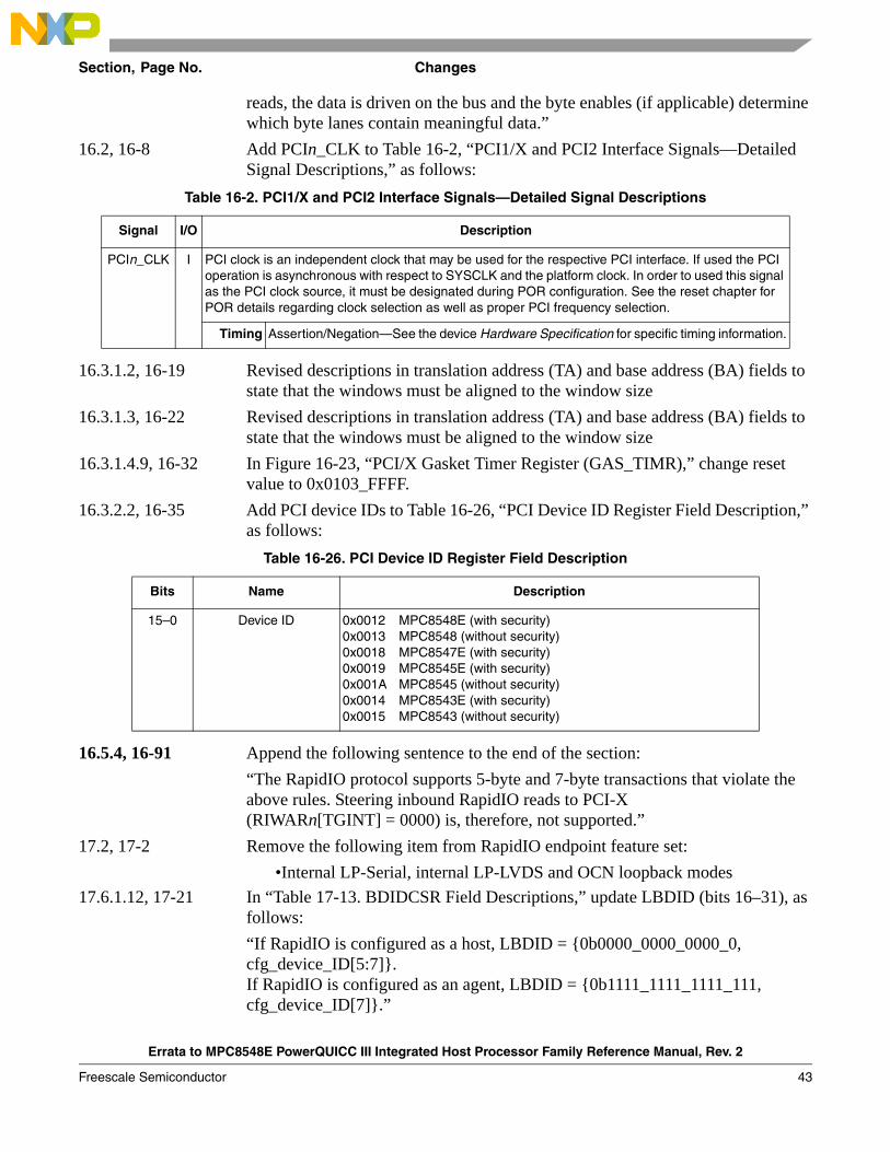
Section, Page No. Changes
Errata to MPC8548E PowerQUICC III Integrated Host Processor Family Reference Manual, Rev. 2
Freescale Semiconductor 43
reads, the data is driven on the bus and the byte enables (if applicable) determine which byte lanes contain meaningful data.”
16.2, 16-8 Add PCIn_CLK to Table 16-2, “PCI1/X and PCI2 Interface Signals—Detailed Signal Descriptions,” as follows:
16.3.1.2, 16-19 Revised descriptions in translation address (TA) and base address (BA) fields to state that the windows must be aligned to the window size
16.3.1.3, 16-22 Revised descriptions in translation address (TA) and base address (BA) fields to state that the windows must be aligned to the window size
16.3.1.4.9, 16-32 In Figure 16-23, “PCI/X Gasket Timer Register (GAS_TIMR),” change reset value to 0x0103_FFFF.
16.3.2.2, 16-35 Add PCI device IDs to Table 16-26, “PCI Device ID Register Field Description,” as follows:
16.5.4, 16-91 Append the following sentence to the end of the section:“The RapidIO protocol supports 5-byte and 7-byte transactions that violate the above rules. Steering inbound RapidIO reads to PCI-X (RIWARn[TGINT] = 0000) is, therefore, not supported.”
17.2, 17-2 Remove the following item from RapidIO endpoint feature set:•Internal LP-Serial, internal LP-LVDS and OCN loopback modes
17.6.1.12, 17-21 In “Table 17-13. BDIDCSR Field Descriptions,” update LBDID (bits 16–31), as follows:“If RapidIO is configured as a host, LBDID = {0b0000_0000_0000_0, cfg_device_ID[5:7]}.If RapidIO is configured as an agent, LBDID = {0b1111_1111_1111_111, cfg_device_ID[7]}.”
Table 16-2. PCI1/X and PCI2 Interface Signals—Detailed Signal Descriptions
Signal I/O Description
PCIn_CLK I PCI clock is an independent clock that may be used for the respective PCI interface. If used the PCI operation is asynchronous with respect to SYSCLK and the platform clock. In order to used this signal as the PCI clock source, it must be designated during POR configuration. See the reset chapter for POR details regarding clock selection as well as proper PCI frequency selection.
Timing Assertion/Negation—See the device Hardware Specification for specific timing information.
Table 16-26. PCI Device ID Register Field Description
Bits Name Description
15–0 Device ID 0x0012 MPC8548E (with security)0x0013 MPC8548 (without security)0x0018 MPC8547E (with security)0x0019 MPC8545E (with security)0x001A MPC8545 (without security)0x0014 MPC8543E (with security)0x0015 MPC8543 (without security)

Section, Page No. Changes
Errata to MPC8548E PowerQUICC III Integrated Host Processor Family Reference Manual, Rev. 2
44 Freescale Semiconductor
17.6.2.2, 17-23 Modify the register description (first paragraph in the section) as follows: “The port link time-out control command and status register (PLTOCCSR), shown in Figure 17-17, contains the link time-out value for all ports on a device. This time-out is for link events such as sending a packet to receiving the corresponding acknowledge and sending a link-request to receiving the corresponding link-response. The reset, or default, value of this counter is the maximum time-out interval. The resolution of this timer is 60/(platform frequency). For example, at a platform frequency of 400 MHz, the maximum timeout value is 0xFF_FFFF * 60/400MHz = 2.52 seconds.”
17.6.2.3, 17-23 Modify the register description (first paragraph in the section) as follows: “The port response time-out control command and status register (PRTOCCSR), shown in Figure 17-18, contains the time-out timer count for all ports on a device. This time-out is for sending a request packet to receiving the corresponding response packet. Note that this applies to the RapidIO endpoint and the messaging unit. The reset, or default, value of this counter is the maximum time-out interval. The resolution of this timer is 60/(platform frequency). For example, at a platform frequency of 400 MHz, the maximum timeout value is 0xFF_FFFF * 60/400MHz = 2.52 seconds.”
17.6.2.2, 17-23 Replace last sentence of first paragraph with the following:“The reset value is the maximum time-out interval. The timer decrements at one-half the platform clock rate; thus at a platform clock rate of 400 MHz, for example, the maximum time-out value is approximately 83.9 ms.”
17.6.2.4, 17-24 In Table 17-19, “GCCSR Field Descriptions,” add the following note to each field description:“Note that although this status bit is R/W, manually changing its value does not affect logical operation.”
17.6.2.7, 17-26 In Section 17.6.2.7, “Local ackID Status Command and Status Register (LASCSR),” update the first paragraph to the following:The local ackID status command and status register (LASCSR) is accessible both by the local processor and an external device. A read to this register returns the local ackID status for both the output and input ports of the device.
17.6.3.2, 17-32 Table 17-26, “LTLEDCSR Field Descriptions,” update ITTE (bit 5) field description, as follows: “Illegal transaction target error.Received a packet that contained a destination ID that is not defined for this end point. Endpoints with multiple ports and a built-in switch function may not report this as an error (transport)”
17.6.3.4, 17-34 In Section 17.6.3.4, “Logical/Transport Layer Address Capture Command and Status Register (LTLACCSR),” update the first paragraph to the following:“The LTLACCSR provides error information. It is locked when a logical/transport error is detected, and the corresponding enable bit is set. LTLACCSR is stored in

Section, Page No. Changes
Errata to MPC8548E PowerQUICC III Integrated Host Processor Family Reference Manual, Rev. 2
Freescale Semiconductor 45
each port and in the message unit, although the values in this register can differ between each port and message unit. The message unit LTLACCSR cannot lock if the message unit or any other port has locked.”
17.6.3.5, 17-35 In Section 17.6.3.5, “Logical/Transport Layer Device ID Capture Command and Status Register (LTLDIDCCSR),” update the first paragraph to the following:“LTLDIDCCSR contains error information. It is locked when a logical/transport error is detected, and the corresponding enable bit is set. LTLDIDCCSR is stored in each port and in the message unit, although the values in this register can differ between each port and message unit. The message unit LTLDIDCCSR cannot lock if the message unit or any other port has locked.”
17.6.3.6, 17-36 In Section 17.6.3.6, “Logical/Transport Layer Control Capture Command and Status Register (LTLCCCSR),” update the first paragraph to the following:“LTLCCCS contains error information. It is stored in each port and in the message unit, although the values in this register can differ between each port and message unit. The message unit LTLCCCSR cannot lock if the message unit or any other port has locked.”
17.6.4.3, 17-39 In Table 17-33, “ECACSR Field Descriptions,” replace description of ECI with the following:
17.6.5.2, 17-44 In Table 17-1, “EPWISR Field Descriptions,” add the following sentence to the PINT (bit 0) field description: “This bit is also set for outbound doorbell packet response time-out (PRT) errors.”
17.6.5.6, 17-45 Update reset value in Figure 17-45, “Accept-All Configuration Register (AACR),” from All zeros to 0x1000_0000.
17.6.5.7, 17-46 Modify the register description (first paragraph in the section) as follows: “The logical outbound packet time-to-live configuration register, shown in Figure 17-46, contains the time-to-live count for all ports on a device. This packet time-to-live counter starts when a packet is ready to be transmitted. If the packet is not successfully transmitted before the timer expires, the packet is discarded. Successfully transmitted means that a packet accept was received for the packet on the RIO interface. If the packet requires a response, an internal error response is returned after the response time-out occurs (PRTOCCSR). The packet time-to-live counter prevents the local processor from being stalled when packets cannot be successfully transmitted (acknowledged with an accept by the link partner at the physical level). The value of this register should always be larger than the link time-out value (PLTOCCSR). When the packet time-to-live counter
Table 17-33. ECACSR Field Descriptions
Bits Name Description
8–23 ECI Extended capture information [0:15].ECI contains the control/data character signal corresponding to each byte of captured data.

Section, Page No. Changes
Errata to MPC8548E PowerQUICC III Integrated Host Processor Family Reference Manual, Rev. 2
46 Freescale Semiconductor
expires, PCR[OBDEN] is automatically set. PCR[OBDEN] must be cleared by software. By default, this time-out value is disabled (all zeros). The resolution of this timer is 60/(platform frequency). For example, at a platform frequency of 400 MHz, the maximum timeout value is 0xFF_FFFF * 60/400MHz = 2.52 seconds.When the packet time-to-live counter expires, PCR[OBDEN] is automatically set. PCR[OBDEN] must be cleared by software.”
17.6.5.7, 17-46 Replace last sentence of first paragraph with the following:“The reset value is the maximum time-out interval. The timer decrements at one-half the platformclock rate; thus at a platform clock rate of 400 MHz, for example, the maximum time-out value is approximately 83.9 ms.”
17.6.5.9, 17-48 In Figure 17-48, “Physical Configuration Register (PCR),” CCP should be represented as a read/write bitfield. The updated definition appears as follows:
17.6.7.8, 17-59 Add the following sentence to the end of the first paragraph:“Note that the LCSBA1CSR register (See Section 17.6.1.11, “Local Configuration Space Base Address 1 Command and Status Register (LCSBA1CSR)”) has priority over all ATMU windows if both are configured for the same address space.”
17.7.1.6, 17-69 In Table 17-71, “OMnDPR Field Descriptions,” the field description of XMAILBOX should reference OMnDATR[MM] instead of OMnMR[MM]. The complete description should read as follows:“Value for ‘xmbox’ field in MESSAGE packet. This field is only used when OMnDATR[MM] is set. For proper operation, this field should only be modified when the outbound message controller is not enabled.”
17.7.1.10, 17-71 The first sentence of the first paragraph should reference OMnDATR[MM] instead of OMnMR[MM]. The corrected sentence should read as follows:“The multicast group register contains a multicast group (MG) value and extended multicast group number (EMG) which, in combination with the multicast list register and the multicast enable (OMnDATR[MM]), indicates which deviceIDs are targets of a multicast operation.”
17.7.2.5, 17-78 Modify the register description (first paragraph in the section) as follows: “The maximum interrupt interval register contains a time-out timer value to define the maximum amount of time that the mailbox controller is to wait from transitioning from not empty to signaling an interrupt (if enabled) to the local processor if the IMnMR[MIQ_THRESH] limit is not reached. The reset, or
Offset 0x1D_0140 Access: Read/Write
0 15 16 17 26 27 28 29 30 31
R— CCC — CCP — OBDEN —
W
Reset 0 0 0 0 0 0 0 0 0 0 0 0 0 0 0 0 1 0 0 0 0 0 0 0 0 0 0 1 0 0 0 0
Figure 17-48. Physical Configuration Register (PCR)

Section, Page No. Changes
Errata to MPC8548E PowerQUICC III Integrated Host Processor Family Reference Manual, Rev. 2
Freescale Semiconductor 47
default, value of this counter is the maximum interrupt interval. The resolution of this timer is 60/(platform frequency). For example, at a platform frequency of 400 MHz, the maximum interval value is 0xFF_FFFF * 60/400MHz = 2.52 seconds.”
17.7.4.1, 17-82 Modify the register description (first paragraph in the section) as follows: “The maximum interrupt interval register contains a time-out timer value to define the maximum amount of time that a doorbell entry can be at the head of the doorbell queue before generating an interrupt (if enabled) if the DIQ_THRESH limit is not reached. The reset, or default, value of this counter is the maximum interrupt interval. The resolution of this timer is 60/(platform frequency). For example, at a platform frequency of 400 MHz, the maximum interval value is 0xFF_FFFF * 60/400MHz = 2.52 seconds.”
17.7.4.3, 17-86 In Table 17-92, “IDQDPAR Field Descriptions,” and Table 17-94, IDQEPAR Field Descriptions,” add the following note to the field description of IDQDPAR[DQDPA] and IDQEPAR[DQEPA], respectively: “Note that this base address must be queue-size aligned.”
17.7.5.3, 17-90 In Table 17-99, “IPWQBAR Field Descriptions,” add the following sentence to the description of PWQBA:“When populating the address in this register it is not necessary to shift the address as the lower 6 bits are merely ignored to ensure cache line alignment.”
17.8.4, 17-95 Remove heading “Inbound Maintenance Accesses.”Revise paragraphs describing configuration access via LCSBA1CSR (the first method), adding bullets that only 32-bit accesses and NREAD or NWRITE_R requests are supported.
17.8.12.2, 17-106 In Table 17-106, “Physical RapidIO Threshold Response,” change references to “EECSR” to correctly read, “ERCSR,” in the second cells (“Error Enable”) of the rows for the following two errors: “Error Rate Counter has exceeded the Degraded Threshold,” and “Error Rate Counter has exceeded the Failed Threshold.”
17.9.4.1, 17-142 In the third bullet following the first paragraph, the reference to OMnMR[MM] should instead reference OMnDATR[MM]. The updated bullet appears as follows:
• Initialize the source address (EOMnSAR, OMnSAR), destination port (OMnDPR), destination attributes (OMnDATR), retry error threshold (OMnRETCR), and double-word count (OMnDCR) registers. If multicast mode is enabled (OMnDATR[MM]) initialize the multicast group and list (OMnMGR, OMnMLR).
17.9.4.1.1, 17-142 Modify first sentence to include contents of first bullet. Remove second sentence and the three following bullets.
17.9.4.1, 17-142 Modify the subsections of Section 17.9.4.1, “Outbound Doorbell Controller,” as follows:

Section, Page No. Changes
Errata to MPC8548E PowerQUICC III Integrated Host Processor Family Reference Manual, Rev. 2
48 Freescale Semiconductor
17.9.4.1.1 Interrupts
The “SRIO outbound doorbell” controller interrupt is generated after the completion of a doorbell (done, error, packet response time-out or retry limit exceeded) if this interrupt event is enabled (ODDATR[EODIE] is a 1). The event that caused this interrupt is indicated by ODSR[EODI]. The interrupt is held until the ODSR[EODI] bit has been cleared by writing a 1.
The “SRIO error/port-write” interrupt can be generated for the following reasons:• RapidIO error response. An interrupt is generated after a RapidIO error response is received and
this interrupt event is enabled (LTLEECSR[MER])• Packet response time-out. An interrupt is generated after a packet response time-out occurs and this
interrupt event is enabled (LTLEECSR[PRT])• Retry error threshold exceeded. An interrupt is generated after a retry threshold exceeded error
occurs and this interrupt event is enabled (LTLEECSR[RETE])
17.9.4.1.2 Error Response Errors
When a RapidIO error response is received by the doorbell controller the following occurs:• The doorbell controller sets the message error response status bits (ODSR[MER] and
LTLEDCSR[MER]) • If LTLEECSR[MER] is set, the interrupt “SRIO error/port-write” is generated.• After the doorbell operation completes (indicated by ODSR[DUB]) the doorbell controller stops.
17.9.4.1.3 Packet Response Time-Out Errors
When a packet response time-out occurs for a doorbell the following occurs:• The doorbell controller sets the packet response time-out status bits (ODSR[PRT] and
LTLEDCSR[PRT]) • If LTLEECSR[PRT] is set, the interrupt “SRIO error/port-write” is generated and EPWISR[PINT]
is set.• After the doorbell operation completes (indicated by ODSR[DUB]) the doorbell controller stops.
17.9.4.1.4 Retry Error Threshold Exceeded Errors
When a retry error threshold exceeded error occurs for a doorbell the following occurs:• The doorbell controller sets the retry threshold exceed status bits (ODSR[RETE] and
LTLEDCSR[RETE]) • If LTLEECSR[RETE] is set, the interrupt “SRIO error/port-write” is generated.• After the doorbell operation completes (indicated by ODSR[DUB]) the doorbell controller stops.
17.9.4.1.5 Error Handling
When an error occurs and the “SRIO error/port-write” interrupt is generated, the following occurs:• Software determines the cause of the interrupt and processes the error
— LTLEDCSR and ODSR capture the error condition for outbound doorbells

Section, Page No. Changes
Errata to MPC8548E PowerQUICC III Integrated Host Processor Family Reference Manual, Rev. 2
Freescale Semiconductor 49
— EPWISR[PINT] is set for PRT error since it is detected by the SRIO controller— Note that LTLEDCSR is a capture once register, so ODSR should be examined to make sure
an outbound doorbell error did not occur immediately after another captured error• Software verifies the doorbell controller has stopped operation by polling ODSR[DUB]• Software disables the doorbell controller by clearing ODMR[DUS]• Software clears the error by writing a 1 to the corresponding outbound doorbell status bits
(ODSR[PRT], ODSR[PRT], and/or ODSR[RETE] as well as LTLEDCSR)
When an error occurs and the “SRIO error/port-write” interrupt is not enabled, the following occurs:• Software determines that an error has occurred by polling the status bits (ODSR[MER],
ODSR[PRT], and/or ODSR[RETE])• Software verifies the doorbell controller has stopped operation by polling ODSR[DUB]• Software disables the doorbell controller by clearing ODMR[DUS]• Software clears the error by writing a 1 to the corresponding status bits (ODSR[MER],
ODSR[PRT], and/or ODSR[RETE])17.9.4.1.3, 17-143 Remove second bullet (beginning “If OMnMR[EIE]is set...”.17.9.4.2.1, 17-150 In the sixth bullet following the first paragraph, the reference to OMnMR[MM]
should instead reference OMnDATR[MM]. The updated bullet appears as follows:
• If using single segment multicast mode, set OMnDATR[MM].17.10.2.1.5, 17-170 Update section, “Error Handling,” as follows:
When an error occurs and the “SRIO error/port-write” interrupt is generated, the following occurs:• Software determines the cause of the interrupt and processes the error
— LTLEDCSR and ODSR capture the error condition for outbound doorbells— EPWISR[PINT] is set for PRT error since it is detected by the SRIO controller— Note that LTLEDCSR is a capture once register, so ODSR should be examined to make sure
an outbound doorbell error did not occur immediately after another captured error• Software verifies the doorbell controller has stopped operation by polling ODSR[DUB]• Software disables the doorbell controller by clearing ODMR[DUS]• Software clears the error by writing a 1 to the corresponding outbound doorbell status bits
(ODSR[PRT], ODSR[PRT], and/or ODSR[RETE] as well as LTLEDCSR)
When an error occurs and the “SRIO error/port-write” interrupt is not enabled, the following occurs:• Software determines that an error has occurred by polling the status bits (ODSR[MER],
ODSR[PRT], and/or ODSR[RETE])• Software verifies the doorbell controller has stopped operation by polling ODSR[DUB]• Software disables the doorbell controller by clearing ODMR[DUS]• Software clears the error by writing a 1 to the corresponding status bits (ODSR[MER],
ODSR[PRT], and/or ODSR[RETE])

Section, Page No. Changes
Errata to MPC8548E PowerQUICC III Integrated Host Processor Family Reference Manual, Rev. 2
50 Freescale Semiconductor
17.10.2.1.2, 17-170 Remove second bullet (beginning “If ODMR[EIE] is set...”)17.10.2.1.4, 17-171 Remove second bullet (beginning “If ODMR[EIE] is set...”)17.10.2.1.7, 17-171 In Table 17-130, “Outbound Doorbell Hardware Errors,” replace all instances of
“ODMR[EIE]” with “OMnMR[EIE].” (All occur in last three rows, in column “Interrupt Generated.”)
17.10.2.1.7, 17-172 In Table 17-130, “Outbound Doorbell Hardware Errors,” “Interrupt Generated” cell for the “error response” row change to read, “SRIO error/port-write if LTLEECSR[MER] set.” “Interrupt Generated” cell for the “number of retries exceeds limit” row change to read, “SRIO error/port-write if LTLEECSR[RETE] set.” “Interrupt Generated” cell for the “packet response time-out” row change to read, “SRIO error/port-write if LTLEECSR[PRT] set.”
17.10.2.2.1, 17-175 Fortify first bullet to read as follows:“Initialize the doorbell queue dequeue pointer address registers (DQDPAR, EDQDPAR) and the doorbell queue enqueue pointer address registers (DQEPAR, EDQEPAR). These need to be initialized to the same value for proper operation. These also must be queue size aligned (in other words, the queue to which they point must be aligned on a boundary equal to number of queue entries ¥ 8 bytes). For example, if there are eight entries in the queue, the queue must be 64-byte aligned.”
18.1.1.1, 18-2 Add the following note at the end of the section:“Note that after reset or when recovering from a link down condition, external transactions should not be attempted until the link has successfully trained. Software can poll the LTSSM state status register (PEX_LTSSM_STAT) to check the status of link training before issuing external requests.”
18.1.2, 18-4 In Section 18.1.2, “PCI Express Features Summary,” update bullets to “Supports eight non-posted and four posted PCI Express inbound transactions” and “Supports up to six internal platform reads and eight internal platform writes for outbound transactions. (The maximum number of outstanding transactions at any given time is eight.)”
18.2, 18-4 Replace Section 18.2, “External Signal Descriptions,” with the following:
18.2 PCI Express Signal Descriptions
PCI Express defines the connection between two devices as a link, which can be composed of a single or multiple lanes. Each lane consists of a differential pair for transmitting (SDn_TX and SDn_TX) and a differential pair for receiving (SDn_RX and SDn_RX) with an embedded data clock.
The PCI Express controller can be configured for a maximum link width of either ×4 or ×8 depending on the cfg_io_ports[0:2] sampled at reset. See Section 4.4.3.5, “I/O Port Selection,” for more information. Note that the PCI Express signals are multiplexed on the SD port with the serial RapidIO signals. Table 18-2, “PCI Express Interface Signals—Detailed Signal Descriptions,” contains detailed descriptions of the external PCI Express interface signals.18-3, 18-5 Added “RC-mode only” to the names of the following registers:

Section, Page No. Changes
Errata to MPC8548E PowerQUICC III Integrated Host Processor Family Reference Manual, Rev. 2
Freescale Semiconductor 51
• PCI Express Slot Capabilities Register (RC-Mode Only)—0x60• PCI Express Slot Control Register (RC-Mode Only)—0x64• PCI Express Slot Status Register (RC-Mode Only)—0x66• PCI Express Root Error Command Register (RC-Mode Only)—0x12C• PCI Express Root Error Status Register (RC-Mode Only)—0x130
18.3, 18-5 Significantly reorganize of the memory map and its subsections. All registers are now categorized under two main categories:
• PCI Express memory-mapped registers• PCI Express configuration-space registers
----------------------------------------------------The following subcategories headings are removed, but the underlying register definitions are preserved as subsections of “Section 18.3.1, “PCI Express Memory Mapped Registers”:
• PCI Express configuration-access registers• PCI Express power-management event and message registers• PCI Express IP-block revision registers• PCI Express ATMU registers• PCI Express error-management registers• PCI Express configuration space access (move under functional
description)The PCI Express configuration space registers are moved under section “PCI Express Configuration Space Registers”. The new structure uses the following subheadings:
• Common PCI Compatible Configuration Header• PCI Compatible Type 0 Configuration Header• PCI Compatible Type 1 Configuration Header• PCI Compatible Device-Specific Configuration Space• PCI Express Extended Configuration Space• PCI Express Controller Internal CSRs
18.3.2.1, 18-9 After the first paragraph in Section 18.3.2.1, “PCI Express Configuration Address Register (PEX_CONFIG_ADDR),” add the following paragraph:“Both root complex (RC) and endpoint (EP) configuration headers contain 4096 bytes of address space. To access a register within the header,both the extended register number and the register number fields are concatenated to form the 4-byte aligned address of the register. That is, the register address is extended to register number 0b00.”
18.3.2.2, 18-10 Add the following sentences to the end of first paragraph:

Section, Page No. Changes
Errata to MPC8548E PowerQUICC III Integrated Host Processor Family Reference Manual, Rev. 2
52 Freescale Semiconductor
“Also note that accesses to the little-endian PCI Express configuration space must be properly formatted. See Section 18.4.1.2.1, “Byte Order for Configuration Transactions,” for more information.”
18.3.2.3, 18-11 In Table 18-6, “PEX_OTB_CPL_TOR Field Descriptions,” replace second sentence of TC field description (begins “One TC unit...”) with the following:“One TC unit is 8× the PCI Express controller clock period; that is, one TC unit is 20 ns at 400 MHz, 24 ns at 333 MHz, and 30 ns at 260 MHz.”
18.3.2.4, 18-12 Update field PEX_CONF_RTY_TOR[TC] to include only bits 8–31. In same section, in Table 18-7, “PEX_CONF_RTY_TOR Field Descriptions,” replace field information with the following:
18.3.5.1.4, 18-23 In Table 18-18, “PEXOWARn Field Descriptions,” update the ROE bit field description as follows:Relaxed ordering enable. When this bit and the RO bit of the PCI Express device control register (described in Section 18.3.9.8, “PCI Express Device Control Register—0x54”) is set, the relaxed ordering bit for the packet is enabled.This bit only applies to memory transactions.0 Default ordering1 Relaxed ordering
18.3.6.1, 18-30 In Table 18-23, “PCI Express Error Detect Register Field Descriptions,” add the following note to PCT bit field description:“Note that a completion timeout counter only starts when the non-posted request was able to send to the link partner.”
18.3.6.6, 18-38 In Table 18-29, “PCI Express Error Capture Register 1 Field Descriptions Internal Source, Outbound Transaction,” replace field description of OD0 with the following:“Internal platform transaction information. Reserved for factory debug.”
18.3.6.6, 18-39 Replace Table 18-30, “PCI Express Error Capture Register 1 Field Descriptions External Source, Inbound Transaction,” and the paragraph that introduces it, with the following:
Table 18-7. PEX_CONF_RTY_TOR Field Descriptions
Bits Name Description
8–31 TC Timeout counter. This is the value that is used to load the response counter of the completion timeout. One TC unit is 8× the PCI Express controller clock period; that is, one TC unit is 20 ns at 400 MHz, and 30 ns at 266.66 MHz. The following are examples of timeout periods based on different TC settings:0x00_0000Reserved0x10_FFFF22.28 ms at 400 MHz controller clock; 33.34 ms at 266.66 MHz controller clock 0xFF_FFFF335.54 ms at 400 MHz controller clock; 503.31 ms at 266.66 MHz controller clock

Section, Page No. Changes
Errata to MPC8548E PowerQUICC III Integrated Host Processor Family Reference Manual, Rev. 2
Freescale Semiconductor 53
Table 18-30 describes the fields of PEX_ERR_CAP_R1 for the case when the FMT and TYPE subfields in PEX_ERR_CAP_R0 (see Table 19-28) indicate the error was caused by an inbound completion transaction.
18.3.6.7, 18-40 Replace Table 18-31, “PCI Express Error Capture Register 2 Field Descriptions Internal Source, Outbound Transaction,” and the paragraph that introduces it, with the following:Table 18-31 describes the fields of PEX_ERR_CAP_R1 for the case when the FMT and TYPE subfields in PEX_ERR_CAP_R0 (see Table 19-28) indicate the error was caused by an inbound memory request transaction.
18.3.6.7, 18-40 Replace Table 18-32, “PCI Express Error Capture Register 2 Field Descriptions External Source, Inbound Transaction,” and the paragraph that introduces it, with the following:Table 18-32 describes the fields of PEX_ERR_CAP_R2 for the case when the FMT and TYPE subfields in PEX_ERR_CAP_R0 (see Table 19-28) indicate the error was caused by an inbound completion transaction.
Table 18-30. PCI Express Error Capture Register 1 Field DescriptionsExternal Source, Inbound Completion Transaction
Bits Name Description
0–31 GH1 PEX second DW (4-byte) header. This field contains the second DW (4-byte) of the captured PCI Express packet header. 24–31 Comp ID[15:8]16–23 Comp ID[7:0]12–15 Byte Count[11:8]11 BCM8–10 Comp Status0–7 Byte Count[7:0]
Table 18-31. PCI Express Error Capture Register 1 Field DescriptionsExternal Source, Inbound Memory Request Transaction
Bits Name Description
0–31 GH1 PEX second DW (4-byte) header. This field contains the second DW (4-byte) of the captured PCI Express packet header. 24–31 Requester ID[15:8]16–23 Requester ID[7:0]8–15 Tag[7:0]4–7 First DW BE[3:0]0–3 Last DW BE[3:0]

Section, Page No. Changes
Errata to MPC8548E PowerQUICC III Integrated Host Processor Family Reference Manual, Rev. 2
54 Freescale Semiconductor
18.3.6.7, 18-41 Replace Table 18-33, “PCI Express Error Capture Register 3 Field Descriptions Internal Source, Outbound Transaction,” and the paragraph that introduces it, with the following:Table 18-33 describes the fields of PEX_ERR_CAP_R2 for the case when the FMT and TYPE subfields in PEX_ERR_CAP_R0 (see Table 19-28) indicate the error was caused by an inbound memory request transaction. Note that PEX_ERR_CAP_R2 captures the 32-bit address for a 3 DW memory request header or the upper half of the 64-bit address for a 4 DW memory request header; the lower half of the 64-bit address for a 4 DW memory request header is captured in PEX_ERR_CAP_R3.
18.3.6.7, 18-41 Replace Table 18-34, “PCI Express Error Capture Register 3 Field Descriptions External Source, Inbound Transaction,” and the paragraph that introduces it, with the following:“Table 18-34 describes the fields of PEX_ERR_CAP_R3 for the case when the FMT and TYPE subfields in PEX_ERR_CAP_R0 (see Table 19-28) indicate the error was caused by an inbound memory request transaction. Note that PEX_ERR_CAP_R3 captures the lower half of the 64-bit address for a 4 DW memory request header; the upper half of the 64-bit address for a 4 DW memory request header or the 32-bit address for a 3 DW memory request header is captured in PEX_ERR_CAP_R2.”
Table 18-32. PCI Express Error Capture Register 2 Field DescriptionsExternal Source, Inbound Completion Transaction
Bits Name Description
0–31 GH2 PEX third DW (4-byte) header. This field contains the third DW (4-byte) of the captured PCI Express packet header. 24–31 Req ID[15:8]16–23 Req ID[7:0]8–15 Tag[7:0]1–7 Lower Address[6:0]0 Reserved
Table 18-33. PCI Express Error Capture Register 2 Field DescriptionsExternal Source, Inbound Memory Request Transaction
Bits NameDescription
3 DW Header 4 DW Header
0–31 GH2 PEX third DW (4-byte) header. This field contains the third DW (4-byte) of the captured PCI Express packet header.
24–31 Address[31:24]16–23 Address[23:16]8–15 Address[15:8]6–7 Reserved0-5 Address[7:2]
24–31 Address[63:56]16–23 Address[55:48]8–15 Address[47:40]0-7 Address[39:32]

Section, Page No. Changes
Errata to MPC8548E PowerQUICC III Integrated Host Processor Family Reference Manual, Rev. 2
Freescale Semiconductor 55
18.3.7, 18-42 The subsection describing PCI Express configuration space access has been moved to Section 18.4, “Functional Description.”
18.3.7.1.1, 18-42 Update the last bulleted item in the list, as follows: “If none of the above conditions occur, then the PCI Express controller returns all 1s for reads and ignores writes. In this case, PEX_ERR_DR[ICCA] is set.”
Table 18-34. PEX Error Capture Register 3 Field DescriptionsExternal Source, Inbound Memory Request Transaction
Bits Name Description
0–31 GH3 PEX fourth DW (4-byte) header. This field contains the fourth DW (4-byte) of the captured PCI Express packet header. 24–31 Address[31:24]16–23 Address[23:16]8–15 Address[15:8]6–7 Reserved0-5 Address[7:2]

Section, Page No. Changes
Errata to MPC8548E PowerQUICC III Integrated Host Processor Family Reference Manual, Rev. 2
56 Freescale Semiconductor
18.3.7.1, 18-42 Add the following to the end of the paragraph:
NOTESAccesses to the little-endian PCI Express configuration space must be properly formatted. See Section 18.4.1.2.1, “Byte Order for Configuration Transactions,” for more information.
External configuration transactions should not be attempted until the link has successfully trained. Software can poll the LTSSM state status register (PEX_LTSSM_STAT) to check the status of link training before issuing external configuration requests.
Refer to Section 18.5.2, “Configuration Accesses and Inbound Writes to CCSR Space,” for special considerations regarding outbound configuration accesses and inbound writes to CCSR space.
18.3.7.1, 18-42 Replace last sentence of first paragraph (begins “Note that the...”) with the following notes:“Note that accesses to the little-endian PCI Express configuration space must be properly formatted. See Section 18.4.1.2.1, “Byte Order for Configuration Transactions,” for more information. Note that external configuration transactions should not be attempted until the link has successfully trained. Software can poll the LTSSM state status register (PEX_LTSSM_STAT) to check the status of link training before issuing external configuration requests.”
18.3.7.2, 18-43 Add statement that the PCI Express controller internal CSR registers are not accessible by inbound PCI Express configuration transactions.
18.3.8.3.11, 18-62 Replace Figure 18-68, “PCI Express Prefetchable Memory Base Register,” with the following:
18.3.8.3.12, 18-63 Replace Figure 18-69, “PCI Express Prefetchable Memory Limit Register,” with the following:
Offset 0x24 Access: Read/Write
15 4 3 0
RPF Memory Base
Address Decode Type
W
Reset 0 0 0 0 0 0 0 0 0 0 0 0 0 0 0 1
Figure 18-68. PCI Express Prefetchable Memory Base Register

Section, Page No. Changes
Errata to MPC8548E PowerQUICC III Integrated Host Processor Family Reference Manual, Rev. 2
Freescale Semiconductor 57
18.3.8.3.15, 18-63 In Figure 18-72, “PCI Express I/O Base Upper 16 Bits Register,” add the following note: “Access is read/write in root complex and read only in endpoint.”
18.3.8.3.16, 18-64 In Figure 18-73, “PCI Express I/O Limit Upper 16 Bits Register,” add the following note: “Access is read/write in root complex and read only in endpoint.”
18.3.8.3, 18-56 Replace the figure in Section “Type 1 Configuration Header,” with the following:
18.3.8.1.2, 18-44 Add PCI Express device ID registers to Table 18-36 as follows:
Offset 0x26 Access: Read/Write
15 4 3 0
RPF Memory Limit
Address Decode Type
W
Reset 0 0 0 0 0 0 0 0 0 0 0 0 0 0 0 1
Figure 18-69. PCI Express Prefetchable Memory Limit Register
ReservedAddress
Offset (Hex)
Device ID Vendor ID 00
Status Command 04
Class Code Revision ID 08
BIST Header Type Latency Timer Cache Line Size 0C
Base Address Register 0 10
14
Secondary Latency Timer Subordinate Bus Number Secondary Bus Number Primary Bus Number 18
Secondary Status I/O Limit I/O Base 1C
Memory Limit Memory Base 20
Prefetchable Memory Limit Prefetchable Memory Base 24
Prefetchable Base Upper 32 Bits 28
Prefetchable Limit Upper 32 Bits 2C
I/O Limit Upper 16 Bits I/O Base Upper 16 Bits 30
Capabilities Pointer 34
Expansion ROM Base Address 38
Bridge Control Interrupt Pin Interrupt Line 3C
Figure 18-58. PCI Express PCI-Compatible Configuration Header—Type 1

Section, Page No. Changes
Errata to MPC8548E PowerQUICC III Integrated Host Processor Family Reference Manual, Rev. 2
58 Freescale Semiconductor
18.3.8.1.3, 18-45 In Table 18-37, “PCI Express Command Register Field Descriptions,” in the description for bit Bus_master, replace RC mode with the following: “RC mode: Clearing this bit disables the ability of the device to forward memory transactions upstream. This causes any inbound memory transaction (except those targeting PEXCSRBAR) to be treated as an unsupported request. Note that the above description does not apply for inbound memory transactions targeting PEXCSRBAR which are forwarded if the Memory_space bit is set.”
18.3.8.1.3, 18-46 In Table 18-37, “PCI Express Command Register Field Descriptions,” in the description for bit Memory_space, replace RC mode with the following: “RC mode: This bit is ignored for inbound memory transactions except those targeting PEXCSRBAR. Clearing this bit prevents the chip from accepting inbound memory transactions to PEXCSRBAR. This bit does not affect outbound memory transactions.”
18.3.8.2, 18-50 In Section 18.3.8.2, “Type 0 Configuration Header,” replace Figure 18-46, “PCI Express PCI-compatible Configuration Header—Type 0,” with the following:
Table 18-36. PCI Express Device ID Register Field Description
Bits Name Description
15–0 Device ID 0x0012 MPC8548E0x0013 MPC85480x0018 MPC8547E0x0019 MPC8545E0x001A MPC85450x0014 MPC8543E0x0015 MPC8543
ReservedAddress
Offset (Hex)
Device ID Vendor ID 00
Status Command 04
Class Code Revision ID 08
BIST Header Type Latency Timer Cache Line Size 0C
Base Address Registers
10
14
18
1C
20
24
28
Subsystem ID Subsystem Vendor ID 2C
Figure 18-46. PCI Express PCI-Compatible Configuration Header—Type 0

Section, Page No. Changes
Errata to MPC8548E PowerQUICC III Integrated Host Processor Family Reference Manual, Rev. 2
Freescale Semiconductor 59
18.3.8.2.6, 18-55 After the first sentence in Section 18.3.8.2.6, “PCI Express Interrupt Pin Register—0x3D,” add the following: “This register only applies to EP mode.”
18.3.8.3.11, 18-62 In Table 18-64, “PCI Express Prefetchable Memory Base Register Field Description,” add following note in bit description 15–4: “Inbound posted transactions hitting into the mem base/limit range are ignored; inbound non-posted transactions hitting into the mem base/limit range results in unsupported request response.”
18.3.8.3.12, 18-62 In Table 18-65, “PCI Express Prefetchable Memory Limit Register Field Description,” add following note in bit description 15–4: “Inbound posted transactions hitting into the mem base/limit range are ignored; inbound non-posted transactions hitting into the mem base/limit range results in unsupported request response.”
18.3.8.3.18, 18-65 In Section 18.3.8.3.18, “PCI Express Interrupt Line Register—0x3C,” in Table 18-71, “PCI Express Interrupt Line Register Field Description,” add the following note to bit 7–0 description: “N/A for RC mode.”
18.3.8.3.19, 18-65 After the first sentence in Section 18.3.8.3.19, “PCI Express Interrupt Pin Register—0x3D,” add the following: “This register only applies to EP mode.”
18.3.9.8, 18-72 In Table 18-81, “PCI Express Device Control Register Field Description,” add following in bit 7–5 description:000 For 128 bytes MAX_PAYLOAD_SIZE001 For 256 bytes MAX_PAYLOAD_SIZEAnd add the following to bit 4 description:1 Relaxed ordering is enabled. Configuration software must clear this bit if Relaxed Ordering is not desired.
18.3.9.10, 18-73 Replace Section 18.3.9.10, “PCI Express Link Capabilities Register—0x58,” with the following:
Expansion ROM Base Address 30
Capabilities Pointer 34
38
MAX_LAT MIN_GNT Interrupt Pin Interrupt Line 3C
ReservedAddress
Offset (Hex)
Figure 18-46. PCI Express PCI-Compatible Configuration Header—Type 0 (continued)

Section, Page No. Changes
Errata to MPC8548E PowerQUICC III Integrated Host Processor Family Reference Manual, Rev. 2
60 Freescale Semiconductor
18.3.9.10 PCI Express Link Capabilities Register—0x58
Offset 0x58 Access: Read only
31 24 23 18 17 15 14 12 11 10 9 4 3 0
R Port Number—
L1_EX_LAT L0s_EX_LAT ASPM MAX_LINK_W MAX_LINK_SP
W
Reset 0 0 0 0 0 0 0 0 0 0 0 0 0 0 1 1 1 1 0 1 0 1 0 0 n n n n 0 0 0 1
Figure 18-88. PCI Express Link Capabilities Register
Table 18-83. PCI Express Link Capabilities Register Field Description
Bits Name Description
31–24 Port Number Port number for PCI Express link
23–18 — Reserved
17–15 L1_EX_LAT L1 exit latencyNote that exit latencies may be influenced by PCI Expressreference clock configuration depending upon whether a component uses a common or separate reference clock.
000 Less than 1 μs001 1 μs to less than 2 μs010 2 μs to less than 4 μs011 4 μs to less than 8 μs100 8 μs to less than 16 μs101 16 μs to less than 32 μs110 32 μs - 64 μs111 More than 64 μs
14–12 L0s_EX_LAT L0s exit latencyNote that exit latencies may be influenced by PCI Expressreference clock configuration depending upon whether a component uses a common or separate reference clock.
000 Less than 64 ns001 64 ns to less than 128 ns010 128 ns to less than 256 ns011 256 ns to less than 512 ns100 512 ns to less than 1 μs101 1 μs to less than 2 μs110 2 μs – 4 μs111 More than 4 μs
11–10 ASPM Active state power management (ASPM) Support
01 L0s entry supported11 L0s and L1entry supported

Section, Page No. Changes
Errata to MPC8548E PowerQUICC III Integrated Host Processor Family Reference Manual, Rev. 2
Freescale Semiconductor 61
18.3.9.11, ,18-74 In Table 18-84, “PCI Express Link Control Register Field Description,” update description of RL field, as follows: “Retrain link (Reserved for EP devices). In RC mode, setting this bit initiates link retraining by directing the Physical Layer LTSSM to the Recovery state, if the link has already been up; reads of this bit always return 0.”
18.3.9.14, 18-75 Replace Table 18-87, “PCI Express Slot Control Register Field Description,” with the following:
9–4 MAX_LINK_W Maximum link width. Reset value depends upon the maximum link width of the PCI Express controller is capable of supporting. 000001: x1000010: x2000100: x4001000: x8
3–0 MAX_LINK_SP Maximum link speed0001 2.5 GT/s link
Table 18-87. PCI Express Slot Control Register Field Description
Bits Name Description
15–11 — Reserved
10 PCC Power controller control.
9–8 PIC Power indicator control.If a power indicator is implemented,set the power indicator to the written state. Reads of this field must reflect the value from the latest write, even if the corresponding hot-plug command is not complete, unless software issues a write without waiting for the previous command to complete in which case the read value is undefined. Defined encodings are:00 Reserved01 On10 Blink11 OffNote: The default value of this field must be one of the non-reserved values. If the power
indicator present bit in the slot capabilities register is 0, this bit is permitted to be read-only with a value of 00.
Table 18-83. PCI Express Link Capabilities Register Field Description (continued)
Bits Name Description

Section, Page No. Changes
Errata to MPC8548E PowerQUICC III Integrated Host Processor Family Reference Manual, Rev. 2
62 Freescale Semiconductor
7–6 AIC Attention indicator control.If an attention indicator is implemented, writes to this field set the attention indicator to the written state. Reads of this field must reflect the value from the latest write, even if the corresponding hot-plug command is not complete, unless software issues a write without waiting for the previous command to complete in which case the read value isundefined.Defined encodings are:00 Reserved01 On10 Blink11 OffNote: The default value of this field must be one of the non- reserved values. if the
attention indicator present bit in the slot capabilities register is 0, this bit is permitted to be readonly with a value of 00.
5 HPIE Hot plug interrupt enable.
4 CCIE Command completed interrupt enable.
3 PDCE Presence detect changed enable.
2 MRLSCE MRL sensor changed enable.
1 PFDE Power fault detected enable.
0 ABPE Attention button pressed enable.
Table 18-87. PCI Express Slot Control Register Field Description (continued)
Bits Name Description

Section, Page No. Changes
Errata to MPC8548E PowerQUICC III Integrated Host Processor Family Reference Manual, Rev. 2
Freescale Semiconductor 63
18.3.9.15, 18-76 Revise reset value for register to 0x48. Also revise bit description for PDS to say, “In the PCI Express specification, this bit indicates the presence of a card in the slot; however, on this device, this bit is set regardless of whether there is a card present or not.” Update Section 18.3.9.15, “PCI Express Slot Status Register—0x66” to Section 18.3.9.15, “PCI Express Slot Status Register (RC-Mode Only)—0x66.”
18.3.10, 18-80 In Figure 18-101, “PCI Express Extended Configuration Space,” update address offset range for PCI Express controller internal CSRs to 0x400–0x6FF. Also add the following footnote to this section of table:PCI Express controller internal CSRs are not accessible by inbound PCI Express configuration transactions. Attempts to access these registers return all 0s.
18.3.10.2, 18-81 In Table 18-97, “PCI Express Uncorrectable Error Status Register Field Description,” add the following note to the CTO bit field description:“Note that a completion timeout error is a fatal error. If a completion timeout error is detected, the system has become unstable. Hot reset is recommended to restore stability of the system.”
18.3.10.5, 18-84 Replace Section 18.3.10.5, “PCI Express Correctable Error Status Register—0x110,” with the following:
18.3.10.5 PCI Express Correctable Error Status Register—0x110
Offset 0x110 Access: w1c
31 1
4
13 12 11 9 8 7 6 5 1 0
R—
ADVNFE
RTTO—
RNR BDLLP BTLP—
RXE
W w1c w1c w1c w1c w1c
Reset All zeros
Figure 18-106. PCI Express Correctable Error Status Register
Table 18-100. PCI Express Correctable Error Status Register Field Description
Bits Name Description
31–14 — Reserved
13 ADVNFE Advisory Non-Fatal Error Status indicates the occurrence of the advisory error, and the Advisory Non-Fatal Error Mask bit in the Correctable Error Mask register is checked to determine whether to proceed further with logging and signaling
12 RTTO Replay timer timeout status
11–9 — Reserved
8 RNR REPLAY_NUM Rollover status
7 BDLLP Bad DLLP status
6 BTLP Bad TLP status

Section, Page No. Changes
Errata to MPC8548E PowerQUICC III Integrated Host Processor Family Reference Manual, Rev. 2
64 Freescale Semiconductor
18.3.10.5, 18-85 Replace Section 18.3.10.5, “PCI Express Correctable Error Mask Register—0x114,” with the following:
18.3.10.6 PCI Express Correctable Error Mask Register—0x114
18.3.10.7, 18-85 In Section 18.3.10.7, “PCI Express Advanced Error Capabilities and Control Register—0x118,” update the reset value to 0000_00B0.
18.3.10.12, 18-88 Change the title of Figure 18-113, “PCI Express Correctable Error Source ID Register,” to Figure 18-113, “PCI Express Error Source ID Register,” and change the title of Table 18-107, “PCI Express Correctable Error Source ID Register Field Description,” to Table 18-107, “PCI Express Error Source ID Register Field Description.”
18.3.10, 18-90 Add the following section after Section 18.3.10.13, “LTSSM State Status Register—0x404”:
5–1 — Reserved
0 RXE Receiver error status
Offset 0x114 Access: Read/Write
3
1
14 13 12 11 9 8 7 6 5 1 0
R—
ADVNFEM
RTTOM — RNRM BDLLPM BTLPM — RXEMW
Reset All zeros
Figure 18-107. PCI Express Correctable Error Mask Register
Table 18-101. PCI Express Correctable Error Mask Register Field Description
Bits Name Description
31–14 — Reserved
13 ADVNFEM Advisory Non-Fatal Error Mask – This bit is Set by default to enable compatibility with software that does not comprehend Role-Based Error Reporting.
12 RTTOM Replay timer timeout mask
11–9 — Reserved
8 RNRM REPLAY_NUM Rollover mask
7 BDLLPM Bad DLLP mask
6 BTLPM Bad TLP mask
5–1 — Reserved
0 RXEM Receiver error mask
Table 18-100. PCI Express Correctable Error Status Register Field Description (continued)
Bits Name Description

Section, Page No. Changes
Errata to MPC8548E PowerQUICC III Integrated Host Processor Family Reference Manual, Rev. 2
Freescale Semiconductor 65
18.3.10.14 N_FTS Control Register—0x41C
The PCI Express N_FTS control register, shown in this figure, is used to set the N_FTS value that is advertised by the PCI Express controller during link training. If this value is changed after the link is up, the new value will take effect during the next link training. The N_FTS value is decided by the L0s exit latency of the RX link of the PHY.
18.3.10.15 PCI Express ACK Replay Time-Out Register—0x438
The PCI Express ACK replay time-out register is used to program time-out values for ACK DLLP transmission and reception in the data link layer. The ACK receive time-out is called the replay time-out since TLPs are re-transmitted after this timeout occurs. Both values should be in terms of PCI Express controller clock cycles.
NOTE When ASPM is enabled, the value of the REPLAY_TIMEOUT field must be adjusted to avoid replay time-out errors. See Section 14.7.4, “Configuring ACK replay time-out when ASPM is enabled,” for more information.
Offset 0x41C Access: Mixed
31 24 23 16 15 8 7 0
RN_FTS_CM_GEN2 N_FTS_GEN2 N_FTS_CM N_FTS
W
Reset All zeros
Figure 18-115. PCI Express N_FTS Control Register (PEX_N_FTS_CTL)
Table 18-110. PEX_N_FTS_CTL Field Descriptions
Bits Name Description
15-8 N_FTS_CM N_FTS common mode. This is the number of Fast Training Sequence (FTS) ordered sets that the PHY requires to enable its RX circuits to achieve bit and symbol lock and come out of ASPM L0s link power state when devices on either side of the link use a common reference clock. This N_FTS value is advertised by the PCI Express controller to the remote device during link training if the common clock configuration (CCC) bit in the Link Control Register is set. At a given time, either N_FTS or N_FTS_CM value is used based on the setting of common clock configuration (CCC) bit in the Link Control Register.
7-0 N_FTS Number of FTSThis is the number of Fast Training Sequence (FTS) ordered sets that the PHY requires to enable its RX circuits to achieve bit and symbol lock and come out of ASPM L0s link power state. This N_FTS value is advertised by the PCI Express controller to the remote device during link training.

Section, Page No. Changes
Errata to MPC8548E PowerQUICC III Integrated Host Processor Family Reference Manual, Rev. 2
66 Freescale Semiconductor
18.3.10.18, 18-93 Replace cross reference in second paragraph to read as follows:“Note that the state of PEX_CFG_READY[CFG_READY] is dependent upon the POR configuration setting described in Section 18.5.1, ‘Boot Mode and Inbound Configuration Transactions.’”
18.4.1.4, 18-100 Add Table 17-119, “PCI Express Controller TLP Transaction Ordering Rules,” which is similar to the way ordering rules are presented in the PCI Express Base Specification, as follows:
Offset 0x438 Access: Read/Write
31 28 27 13 12 0
R— REPLAY_TIMEOUT ACK_LATENCY_TIMEOUT
W
Reset 0 0 0 0 0 0 0 1 1 1 1 1 1 1 0 0 0 0 0 1 1 1 1 0 0 0 1 0 0 0 0 0
Figure 18-116. PCI Express ACK Replay Time-Out Register
Table 18-111. PCI Express ACK Replay Time-Out Register Field Descriptions
Bits Name Description
31–28 — Reserved
27–13 REPLAY_TIMEOUT
Time-out value to wait for reception of ACK DLLP from link side by DLL before re-transmitting TLPs.
12–0 ACK_LATENCY_TIMEOUT
Time-out value to force transmission of ACK DLLP by DLL after a TLP is received.
Table 17-119. PCI Express Controller TLP Transaction Ordering Rules
Row Pass Column?
Posted Request
Non-posted Request Completion
Memory Write or Message
Request (Col 2)
Read Request (Col 3)
I/O or Configuration Write Request
(Col 4)
Read Completion
(Col 5)
I/O or Configuration
Write Completion
(Col 6)
Posted Request
Memory Write or Message
Request (Row A)
a) No1
b) No1Yes Yes a) Yes2
b) N/A3a) Yes2
b) N/A3

Section, Page No. Changes
Errata to MPC8548E PowerQUICC III Integrated Host Processor Family Reference Manual, Rev. 2
Freescale Semiconductor 67
18.4.1.8, 18-101 Revised first paragraph by removing “originating from the PCI Express outbound ATMUs” from the first sentence. Also, remove the last sentence that stated, “Note that configuration writes originating from the PCI Express configuration access registers (PEX_CONFIG_ADDR/PEX_CONFIG_DATA) are not serialized.”
18.4.1.9.1, 18-102 Update the second paragraph, as follows:“Part of the 4-byte data is used to store information such as message code and routing information. Table 18-119 describes the message data format.”
18.4.1.9.1, 18-103 In Table 18-120, “PCI Express ATMU Outbound Messages,” change several outbound messages to be supported in EP mode. The affected rows appear as follows:
Non-posted Request
Read Request (Row B)
No No No a) No4
b) Yes5a) No4
b) Yes5
I/O or Configuration Write Request
(Row C)
No No No a) No4
b) Yes5a) No4
b) Yes5
Completion
Read Completion
(Row D)
a) No6
b) Yes7Yes Yes a) No8
b) No8No
I/O or Configuration
Write Completion
(Row E)
a) No6
b) Yes7Yes Yes No No
1 Regardless of the setting of the relaxed ordering (RO) bit, a posted request cannot bypass another posted request.2 Regardless of the setting of the relaxed ordering bit, a posted request can always bypass a completion.3 N/A indicates that the original rules at these entries defined by the PCI Express Base Specification do not apply to RC or EP.4 A non-posted request cannot bypass a completion if the relaxed ordering bit is cleared (that is, RO = 0).5 A non-posted request can bypass a completion if the relaxed ordering bit is set (that is, RO = 1).6 A read completion, I/O write completion, or configuration write completion cannot bypass a posted request if the relaxed
ordering bit is cleared (that is, RO = 0).7 A read completion, I/O write completion, or configuration write completion can bypass a posted request if the relaxed ordering
bit is set (that is, RO = 1).8 Regardless of the setting of the relaxed ordering bit, a read completion cannot bypass another read completion.
Table 17-119. PCI Express Controller TLP Transaction Ordering Rules (continued)
Row Pass Column?
Posted Request
Non-posted Request Completion
Memory Write or Message
Request (Col 2)
Read Request (Col 3)
I/O or Configuration Write Request
(Col 4)
Read Completion
(Col 5)
I/O or Configuration
Write Completion
(Col 6)

Section, Page No. Changes
Errata to MPC8548E PowerQUICC III Integrated Host Processor Family Reference Manual, Rev. 2
68 Freescale Semiconductor
18.4.1.10, 18-105 Add Section 18.4.1.10, “Error Handling,” as follows:
18.4.1.10 Error Handling
The PCI Express specification classifies errors as correctable and uncorrectable. Correctable errors result in degraded performance, but uncorrectable errors generally result in functional failures. As shown in Figure 18-130 uncorrectable errors can further be classified as fatal or non-fatal.
Figure 18-130. PCI Express Error Classification
18.4.1.10.1 PCI Express Error Logging and Signaling
Figure 18-131 shows the PCI Express-defined sequence of operations related to signaling and logging of errors detected by a device. Note that the PCI Express controller on this device supports the advanced error handling capabilities shown within the dotted lines.
Table 18-120. PCI Express ATMU Outbound Messages
Name Code[7:0] Routing[2:0] RC EP Description
Assert_INTA 0010 0000 100 N/A Yes Sent upstream by endpoint
Assert_INTB 0010 0001 100 N/A Yes Sent upstream by endpoint
Assert_INTC 0010 0010 100 N/A Yes Sent upstream by endpoint
Assert_INTD 0010 0011 100 N/A Yes Sent upstream by endpoint
Deassert_INTA 0010 0100 100 N/A Yes Sent upstream by endpoint
Deassert_INTB 0010 0101 100 N/A Yes Sent upstream by endpoint
Deassert_INTC 0010 0110 100 N/A Yes Sent upstream by endpoint
Deassert_INTD 0010 0111 100 N/A Yes Sent upstream by endpoint
Physical
Data Link Transaction
Correctable Errors
ERR_COR
Physical
Transaction
Uncorrectable Errors
ERR_NONFATAL
Data Link
ERR_FATAL
Fatal

Section, Page No. Changes
Errata to MPC8548E PowerQUICC III Integrated Host Processor Family Reference Manual, Rev. 2
Freescale Semiconductor 69
Figure 18-131. PCI Express Device Error Signaling Flowchart
If First Error Pointer not valid,update First Error Pointerand Header Log Registers
Set corresponding bit inUncorrectable Error
Status Register
Masked inUncorrectable
Error MaskRegister
?
Set Fatal/Non_FatalError Detected bit in
Device Status Register
Adjust severity accordingto Uncorrectable Error
Severity Register
UncorrectableError Reporting Enabled
in Device ControlRegister
?
Is severity Fatal?
Send ERR_NONFATALMessage (See Note)
Send ERR_FATALMessage (See Note)
End
End
End
Send ERR_CORMessage (See Note)
CorrectableError Reporting Enabled
in Device ControlRegister
?
Masked inCorrectableError Mask
Register?
End
Set corresponding bit inCorrectable ErrorStatus Register
Set CorrectableError Detected bit in
Device Status Register
End
End
Correctable?
Error Detected
NOTE: If error is detected by theRoot Port, the error message is notactually sent, but is processedinternally by the Root Port (i.e. raising interrupt).
End
YesNo
Yes
No
Yes
No
Yes
No
Yes
No
No
Yes
Advanced ErrorHandling Only

Section, Page No. Changes
Errata to MPC8548E PowerQUICC III Integrated Host Processor Family Reference Manual, Rev. 2
70 Freescale Semiconductor
18.4.1.10.2 PCI Express Controller Internal Interrupt Sources
Table 18-123 describes the sources of the PCI Express controller internal interrupt to the PIC and the preconditions for signaling the interrupt.
Table 18-123. PCI Express Internal Controller Interrupt Sources
Status Register Bit Preconditions
Any bit in PEX_PME_MES_DR set The corresponding interrupt enable bits must be set in PEX_PME_MES_IER
Any bit in PEX_ERR_DR set The corresponding interrupt enable bits must be set in PEX_ERR_EN.
PCI Express Root Status Register[16] (PME status) is set
PCI Express Root Control Register [3] (PME interrupt enable) is set
PCI Express Root Error Status Register[6] (fatal error messages received) is set
PCI Express Root Error Command Register [2] (fatal error reporting enable) is set orPCI Express Root Control Register [2] (system error on fatal error enable) is set
PCI Express Root Error Status Register [5] (non-fatal error messages received) is set
PCI Express Root Error Command Register [1] (non-fatal error reporting enable) is set or PCI Express Root Control Register [1] (system error on non-fatal error enable) is set
PCI Express Root Error Status Register[0] (correctable error messages received) is set
PCI Express Root Error Command Register[0] (correctable error reporting enable) is setor PCI Express Root Control Register[0] (system error on correctable error enable) is set.
Any correctable error status bit in PCI Express Correctable Error Status Register is set
The corresponding error mask bit in PCI Express Correctable Error Mask Register is clear and PCI Express Root Error Command Register[0] (correctable error reporting enable) is set
Any fatal uncorrectable error status bit in PCI Express Uncorrectable Error Status Register is set. (The corresponding error is classified as fatal based on the severity setting in PCI Express Uncorrectable Error Severity Register.)
The corresponding error mask bit in PCI Express Uncorrectable Error Mask Register is clear and either PCI Express Device Control Register[2] (fatal error reporting) is set or PCI Express Command Register[8] (SERR) is set.
Any non-fatal uncorrectable error status bit in PCI Express Uncorrectable Error Status Register is set. (The corresponding error is classified as non-fatal based on the severity setting in PCI Express Uncorrectable Error Severity Register.)
The corresponding error mask bit in PCI Express Uncorrectable Error Mask Register is clear and either PCI Express Device Control Register[1] (non-fatal error reporting) is set or PCI Express Command Register[8] (SERR) is set.
PCI Express Secondary Status Register[8] (master data parity error) is set.
PCI Express Secondary Status Interrupt Mask Register[0] (mask master data parity error) is cleared and PCI Express Command Register[6] (parity error response) is set.
PCI Express Secondary Status Register[11] (signaled target abort) is set
PCI Express Secondary Status Interrupt Mask Register[1] (mask signaled target abort) is cleared.
PCI Express Secondary Status Register[12] (received target abort) is set
PCI Express Secondary Status Interrupt Mask Register[2] (mask received target abort) is cleared.

Section, Page No. Changes
Errata to MPC8548E PowerQUICC III Integrated Host Processor Family Reference Manual, Rev. 2
Freescale Semiconductor 71
PCI Express Secondary Status Register[13] (received master abort) is set
PCI Express Secondary Status Interrupt Mask Register[3] (mask received master abort) is cleared.
PCI Express Secondary Status Register[14] (signaled system error) is set.
PCI Express Secondary Status Interrupt Mask Register[4] (mask signaled system error) is cleared.
PCI Express Secondary Status Register[15] (detected parity error) is set
PCI Express Secondary Status Interrupt Mask Register[5] (mask detected parity error) is cleared.
PCI Express Slot Status Register[0] (attention button pressed) is set
PCI Express Slot Control Register[0] (attention button pressed enable) is set and PCI Express Slot Control Register[5] (hot plug interrupt enable) is set and either PCI Express PM Control Register[1–0] = 00 (the function power state is D0) or PCI Express PM Control Register[8] (PME enable) is set.
PCI Express Slot Status Register[1] (power fault detected) is set
PCI Express Slot Control Register[1] (power fault detected enable) is set and PCI Express Slot Control Register[5] (hot plug interrupt enable) is set and either PCI Express PM Control Register[1–0] = 00 (the function power state is D0) or PCI Express PM Control Register[8] (PME enable) is set.
PCI Express Slot Status Register[2] (MRL sensor changed) is set
PCI Express Slot Control Register[2] (MRL sensor changed enable) is set and PCI Express Slot Control Register[5] (hot plug interrupt enable) is set and either PCI Express PM Control Register[1–0] = 00 (the function power state is D0) or PCI Express PM Control Register[8] (PME enable) is set.
PCI Express Slot Status Register[3] (presence detect changed) is set
PCI Express Slot Control Register[3] (presence detect changed enable) is set and PCI Express Slot Control Register[5] (hot plug interrupt enable) is set and either PCI Express PM Control Register[1–0] = 00 (the function power state is D0) or PCI Express PM Control Register[8] (PME enable) is set.
PCI Express Slot Status Register[4] (command completed) is set
PCI Express Slot Control Register[4] (command completed interrupt enable) is set and PCI Express Slot Control Register[5] (hot plug interrupt enable) is set.
Table 18-123. PCI Express Internal Controller Interrupt Sources (continued)
Status Register Bit Preconditions

Section, Page No. Changes
Errata to MPC8548E PowerQUICC III Integrated Host Processor Family Reference Manual, Rev. 2
72 Freescale Semiconductor
18.4.1.10.3 Error Conditions
Table 18-124 describes specific error types and the action taken for various transaction types.Table 18-124. Error Conditions
Transaction Type
Error Type Action
Inbound response
PEX response time out. This case happens when the internal platform sends a non-posted request that did not get a response back after a specific amount of time specified in the outbound completion timeout register (PEX_OTB_CPL_TOR)
Log error (PEX_ERR_DR[PCT]) and send interrupt to PIC, if enabled.
Inbound response
Unexpected PEX response. This can happen if, after the response times out and the internal queue entry is deallocated, the response comes back.
Log unexpected completion error (PCI Express Uncorrectable Status Register[16]) and send interrupt to PIC, if enabled.
Inbound response
Unsupported request (UR) response status
Depending upon whether the initial internal request was broken up, the error will not be sent until all responses come back for all portions of the internal request. Log the error (PEX_ERR_DR[CDNSC] and PCI Express Uncorrectable Status Register[20]) and send interrupt to PIC, if enabled.
Inbound response
Completer abort (CA) response status
Depending upon whether the initial internal request was broken up, the error will not be sent until all responses come back for all portions of the internal request. Log the error (PEX_ERR_DR[PCAC, CDNSC] and PCI Express Uncorrectable Status Register[15] and send interrupt to PIC, if enabled.
Inbound response
Poisoned TLP (EP=1) Depending upon whether the initial internal request was broken up, the error will not be sent until all responses come back for all portions of the internal request. Log the error (PCI Express Uncorrectable Status Register[12]) and send interrupt to PIC, if enabled.
Inbound response
ECRC error Depending upon whether the initial internal request was broken up, the error will not be sent until all responses come back for all portions of the internal request. Log the error (PCI Express Uncorrectable Status Register[19]) and send interrupt to PIC, if enabled.
Inbound response
Configuration Request Retry Status (CRS) timeout for a configuration transaction that originates from PEX_CONFIG_ADDR/PEX_CONFIG_DATA
1.The controller always retries the transaction as soon as possible until a status other than CRS is returned. However, if a CRS status is returned after the configuration retry timeout (PEXCONF_RTY_TOR) timer expires, then the controller aborts the transaction and sends all 1s (0xFFFF_FFFF) data back to requester. 2. Log the error (PEX_ERR_DR[PCT]) and send interrupt to the PIC, if enabled.

Section, Page No. Changes
Errata to MPC8548E PowerQUICC III Integrated Host Processor Family Reference Manual, Rev. 2
Freescale Semiconductor 73
Inbound response
UR response for configuration transaction that originates from PEX_CONFIG_ADDR/PEX_CONFIG_DATA
1. Send back all 1s (0xFFFF_FFFF) data.2. Log the error (PEX_ERR_DR[CDNSC] and PCI Express Uncorrectable Status Register[20]) and send interrupt to PIC, if enabled.
Inbound response
CA response for Configuration transaction that originates from PEX_CONFIG_ADDR/PEX_CONFIG_DATA
1. Send back all 1s (0xFFFF_FFFF) data.2. Log the error (PEX_ERR_DR[PCAC, CDNSC] and PCI Express Uncorrectable Status Register[15]) and send interrupt to PIC, if enabled.
Inbound response
Poisoned TLP (EP=1) response for Configuration transaction that originates from PEX_CONFIG_ADDR/PEX_CONFIG_DATA
1. Send back all 1s (0xFFFF_FFFF) data.2. Log the error (PCI Express Uncorrectable Status Register[12]) and send interrupt to PIC, if enabled.
Inbound response
ECRC error response for Configuration transaction that originates from PEX_CONFIG_ADDR/PEX_CONFIG_DATA
1. Send back all 1s (0xFFFF_FFFF) data.2. Log the error (PCI Express Uncorrectable Status Register[19]) and send interrupt to PIC, if enabled.
Inbound response
Configuration Request Retry Status (CRS) response for Configuration transaction that originates from ATMU
1.The controller always retries the transaction as soon as possible until a status other than CRS is returned. However, if a CRS status is returned after the configuration retry timeout (PEXCONF_RTY_TOR) timer expires, then the controller aborts the transaction. 2. Log the error (PEX_ERR_DR[CRST]) and send interrupt to the PIC, if enabled.
Inbound response
UR response for Configuration transaction that originates from ATMU
Log the error (PEX_ERR_DR[CDNSC] and PCI Express Uncorrectable Status Register[20]) and send interrupt to PIC, if enabled.
Inbound response
CA response for Configuration transaction that originates from ATMU
Log the error (PEX_ERR_DR[PCAC, CDNSC] and PCI Express Uncorrectable Status Register[15]) and send interrupt to PIC, if enabled.
Inbound response
Malformed TLP response PCI Express controller will not pass the response back to the core. Therefore, a completion timeout error will eventually occur.
Inbound request
Poisoned TLP (EP=1) 1. If it is a posted transaction, the controller will drop it. 2. If it is a non-posted transaction, the controller will return a completion with UR status.3. Release the proper credits
Inbound request
ECRC error 1. If it is a posted transaction, the controller will drop it. 2. If it is a non-posted transaction, the controller will return a completion with UR status.3. Release the proper credits
Inbound request
PCI Express nullified request The packet is dropped.
Outbound request
Outbound ATMU crossing Log the error (PEX_ERR_DR[OAC]). The transaction will not be sent out on the link.
Table 18-124. Error Conditions (continued)
Transaction Type
Error Type Action

Section, Page No. Changes
Errata to MPC8548E PowerQUICC III Integrated Host Processor Family Reference Manual, Rev. 2
74 Freescale Semiconductor
18.4.2.1.3, 18-106 Replace paragraph with the following:“Software can generate outbound assert or deassert INTx message transactions by using the outbound ATMU mechanism described in Section 18.4.1.9.1, ‘Outbound ATMU Message Generation.’”
18.5, 18-108 Add Section 18.5.2, “Configuration Accesses and Inbound Writes to CCSR Space,” as follows:
18.5.2 Configuration Accesses and Inbound Writes to CCSR Space
In RC mode, when the core issues an outbound configuration access to an external device using the PCI Express configuration access registers (PEX_CONFIG_ADDR/PEX_CONFIG_DATA), there is a potential deadlock if several inbound memory write transactions targeting the CCSR space are received before the completion for the configuration access is returned. Inbound writes to CCSR space include MSIs and message interrupts to the MPIC. The deadlock also can occur when the endpoint generates a single write to CCSR followed by multiple writes to another target before the original configuration access by the RC completes. When the deadlock occurs the configuration access will time out and an error will be reported (if enabled). This deadlock can be avoided by any of the following methods:
1. Configure external agents to allow completions to bypass memory write requests. Many devices allow this when relaxed ordering (RO) is in effect; however, this ability is optional under the PCI Express Base Specification ordering rules, so it is possible that some devices may not support it.
2. For the RC, restrict external configuration accesses through PEX_CONFIG_ADDR/ PEX_CONFIG_DATA to the enumeration of the bus and other initialization functions; do not use PEX_CONFIG_ADDR/PEX_CONFIG_DATA to access external devices during periods when PCI Express endpoints are generating inbound writes to CCSR space.
Outbound request
Illegal message size Log the error (PEX_ERR_DR[MIS]). The transaction will not be sent out on the link.
Outbound request
Illegal I/O size Log the error (PEX_ERR_DR[IOIS]). The transaction will not be sent out on the link.
Outbound request
Illegal I/O address Log the error (PEX_ERR_DR[IOIA]). The transaction will not be sent out on the link.
Outbound request
Illegal configuration size Log the error (PEX_ERR_DR[CIS]). The transaction will not be sent out on the link.
Outbound response
Internal platform response with error (for example, an ECC error on a DDR read or the transaction maps to unknown address space).
Send poisoned TLP (EP=1) completion(s) for data that are known bad. If the poison data happens in the middle of the packet, the rest of the response packet(s) is also poisoned.
Table 18-124. Error Conditions (continued)
Transaction Type
Error Type Action

Section, Page No. Changes
Errata to MPC8548E PowerQUICC III Integrated Host Processor Family Reference Manual, Rev. 2
Freescale Semiconductor 75
3. Govern the generation of write transactions by the endpoint device such that after a write to the CCSR space no other writes are generated until pending configuration accesses are completed or the write is guaranteed to have completed by the completion of a subsequent read request by the endpoint devices.
4. Use the PCI Express outbound ATMU window to generate outbound configuration accesses during periods when an endpoint device may be writing to CCSR space. See Section 18.3.7.1.2, “Outbound ATMU Configuration Mechanism (RC-Only),” for more information. The deadlock does not occur when the ATMU window is used for configuration accesses.
18.5, 18-108 Add Section 18.5.3, “Configuring ACK replay time-out when ASPM is enabled,” as follows:
18.5.3 Configuring ACK replay time-out when ASPM is enabled
When ASPM is enabled, the REPLAY_TIMEOUT value in the PCI Express ACK replay time-out register must be adjusted to avoid replay timeout errors. In this case, the REPLAY_TIMEOUT value should be calculated as follows:
1. Read PCI Express N_FTS control register (PEX_N_FTS_CTL) and take the appropriate N_FTS value:
2. Add 1024 +16 to the value in Step 1.3. Multiply the result of Step 2 by 4 symbol times or 4/PIPE clock frequency, where PIPE clock
frequency is either 250 MHz for 2.5 Gbps operation or 500 MHz for 5.0 Gbps operation. 4. Multiply the result of Step 3 by the PCI Express controller (CORE) clock frequency/PIPE clock
frequency. See Section 18.3.10.14, “PCI Express Controller Core Clock Ratio Register—0x440,” for information about the PCI Express controller clock frequency.
Use the result of Step 4 to update the REPLAY_TIMEOUT value in the PCI Express ACK replay time-out register. As an equation, this value can be expressed:
For example, given the following conditions:• The platform clock frequency is 600 MHz
Table 18-125. PEX_N_FTS_CTL field selection
PEX_N_FTS_CTL field Link speed
Common clock mode
N_FTS 2.5 Gbps No
N_FTS_CM 2.5 Gbps Yes
N_FTS 1024 16+ +( ) 4PIPE_clk----------------------× PCI_Express_controller_clk
PIPE_clk--------------------------------------------------------------------×

Section, Page No. Changes
Errata to MPC8548E PowerQUICC III Integrated Host Processor Family Reference Manual, Rev. 2
76 Freescale Semiconductor
• The PCIe link speed is 5.0 Gbps• The PCI Express controller clock is platform_freq/2• The reset value of PEX_N_FTS_CTL is 40404040h• The common clock configuration bit (CCC) in the Link Control Register is set
Determine the new value for REPLAY_TIMEOUT by following the steps:1. N_FTS_GEN2 = 40h = 64d
Use N_FTS_CM_GEN2 because the link speed is 5.0 Gbps and the common clock configuration bit is set.
2. 64 + 1024 + 16 = 11043. 1104 × (4/500 MHz) = 1104 × 8 ns = 8832 ns
Use 500 MHz for the PIPE_clk because the link speed is 5.0 Gbps.4. 8832 × (300/500) = 5299.2
Use 300 MHz for PCI_Express_controller_clk because the platform clock frequency is 600 MHz and the PCI Express controller clock frequency is platform_freq/2. Use 500 MHz for the PIPE_clk because the link speed is 5.0 Gbps.
Rounding up to 5300, the new value for REPLAY_TIMEOUT should be 14B4h.”
18.4.6, 18-109 Add Section 18.4.6, “Link Down,” as follows:“Typically, a link down condition occurs after a hot reset event; however, it is possible for the link to go down unexpectedly without a hot reset event. When this occurs, a link down condition is detected (PEX_PME_MSG_DR[LDD]=1). Link down is treated similarly to a hot reset condition. Subsequently, while the link is down, all new posted outbound transactions will be discarded. All new non-posted ATMU transactions will be errored out. Non-posted configuration transactions issued using PEX_CONFIG_ADDR/PEX_CONFIG_DATA toward the link will return 0xFFFF_FFFF (all 1s). As soon as the link is up again, the sending of transaction resumes. Note that in EP mode, a link down condition causes the controller to reset all non-sticky bits in its PCI Express configuration registers as if it had been hot reset.”
19.2, 19-13 In Table 19-3, “SEC Address Map,” update register ranges of AESU context registers and key memory registers in the memory map, according to the following:AESU context memory registers: originally, 0x3_4100–0x3_4108; now, 0x3_4100–0x3_4137AESU key memory: originally, 0x3_4400–0x3_4408; now, 0x3_4400–0x3_441F
19.4.6.9.1, 19-76 Modify the bulleted list to say the following:• Context register 1 holds the most significant bytes of the initialization vector
(bytes 1–8).

Section, Page No. Changes
Errata to MPC8548E PowerQUICC III Integrated Host Processor Family Reference Manual, Rev. 2
Freescale Semiconductor 77
• Context register 2 holds the least significant bytes of the initialization vector (bytes 9–16).
19.4.6.9.2, 19-76 Replace last sentence of paragraph with the following:The value of M is specified by writing to context register 7 as described in Figure 19-60.
19.4.7, 19-79 Replace Section 19.4.7, “Kasumi Execution Unit (KEU),” and subsections with the following:
19.4.7 Kasumi Execution Unit (KEU)
This section contains details about the Kasumi execution unit (KEU), including modes of operation, status and control registers, and FIFOs. The KEU has been designed to support the F8 confidentiality function of the 3GPP, GSM A5/3, EDGE A5/3, and GPRS GEA3 algorithms. The KEU also supports the 3GPP F9 integrity function.
Most of the registers described here would not normally be accessed by the host. They are documented here mainly for debug purpose. In typical operation, the KEU is used through channel-controlled access, which means that most reads and writes of the KEU registers are directed by the SEC channels. Driver software performs host-controlled register accesses only on a few registers for initial configuration and error handling.
This execution unit (EU) includes an ICV checking feature, which means it can generate an ICV and compare it to another supplied ICV. The pass/fail result of this ICV check can be returned to the host either through interrupt or by using a writeback of EU status fields into the host memory, but not using both methods at the same time.
To signal the ICV checking result by status writeback, turn on either the IWSE bit or AWSE bit in the crypto-channel configuration register (see Section 19.5.1.1, “Crypto-Channel Configuration Registers 1–4 (CCCRn),” and mask the ICE bit in the interrupt mask register (Section 19.4.7.7, “KEU Interrupt Mask Register (KEUIMR)”). In this case the normal DONE signal (by interrupt or writeback) is undisturbed.
To signal the ICV checking result by interrupt, unmask the ICE bit in the interrupt mask register and turn off the IWSE and AWSE bits in the channel configuration register. If there is no ICV mismatch, the normal DONE signal (by interrupt or writeback) occurs. When there is an ICV mismatch, there is an ERROR interrupt signal to the host, but no DONE interrupt signal or writeback.
19.4.7.1 KEU Mode Register (KEUMR)
The KEU mode registe contains several bits which are used to program the KEU. The mode register is cleared when the KEU is reset or re-initialized. Setting a reserved mode bit generates a data error. Setting both the GSM and EDGE bits to one generates a data error. If the KEU mode register is modified during processing, a context error is generated.

Section, Page No. Changes
Errata to MPC8548E PowerQUICC III Integrated Host Processor Family Reference Manual, Rev. 2
78 Freescale Semiconductor
This table describes the KEU mode register fields.
Address KEU 0x3_E000 Access: Read/write
0 55 56 57 58 59 60 61 62 63
R— GSM CICV EDGE PE INT — ALG
W
Reset All zeros
Figure 19-57. KEU Mode Register
Table 19-44. KEU Mode Register Field Descriptions
Bits Name Description
0–55 — Reserved
56 GSM Select GSM A5/3 blocks0 GSM A5/3 blocks not selected1 GSM A5/3 blocks selectedNote 1: For GSM A5/3, Two 114-bit blocks are required to be produced each 4.615mS slot. If GSM = 1, the first
read of the output FIFO retrieves the first 64 bits of block 1. The second read of the output FIFO retrieves the next 50 bits of block 1 (the remaining bits of this 64-bit word are set to zero). The third read of the output FIFO retrieves the first 64 bits of block 2, while a fourth read of the output FIFO retrieves the next 50 bits of block 2 (the remaining bits of this 64-bit word are set to zero).
Note 2: If GSM = 0, 228 contiguous bits may be read with successive reads of the output FIFO. In this case the host (application) will be responsible for handling the A5/3 block formatting.
Note 3: If GSM is set to 1, while EDGE = 1, an interrupt/error will be generated.
57 CICV Compare integrity check values.0 Normal operation; no ICV comparison.1 After the ICV is computed, compare it to the data in the KEU’s ICV_In register. If the ICVs do not match, send
an error interrupt to the channel. Only applicable when the ALG field is set to a function that uses F9.
58 EDGE Select EDGE A5/3 blocks0 EDGE A5/3 blocks not selected1 EDGE A5/3 blocks selectedNote 1: For EDGE A5/3, two 348-bit blocks are required to be produced each 4.615mS slot. If EDGE = 1, the
first five reads of the output FIFO retrieve the first 320 bits of block 1. The sixth read of the output FIFO retrieves the final 28 bits of block 1 (the remaining bits of the sixth 64-bit word are set to zero). The next five reads of the output FIFO retrieve the first 320 bits of block 2. The following read of the output FIFO retrieves the final 28 bits of block 2 (the remaining bits of this 64-bit word are set to zero).
Note 2: If EDGE = 0, 696 contiguous bits may be read with successive reads of the output FIFO. In this case the host (application) will be responsible for handling the A5/3 block formatting.
Note 3: If EDGE is set to 1, whilst GSM = 1, an interrupt/error will be generated.
59 PE Process end of message. Enables final processing of last message block (F9 only).0 Prevent final block processing (message incomplete)1 Enable final block processing (message complete)Note: As the use of PE is tightly coupled with the use of the KEU data size register, see Section 19.4.7.3, “KEU
Data Size Register (KEUDSR)” for more details.
60 INT Initialization. Enables initialization for a new message. 0 Prevent initialization1 Enable initializationNote: For F8 or F9 operations, if the 3G frame (or message) is being processed through a single descriptor, the
Initialization bit should be set. If the frame is split across multiple descriptors, this bit should only be set in the descriptor that processes the first block of the message.

Section, Page No. Changes
Errata to MPC8548E PowerQUICC III Integrated Host Processor Family Reference Manual, Rev. 2
Freescale Semiconductor 79
19.4.7.2 KEU Key Size Register (KEUKSR)
The KEU key size register stores the number of bytes in the key. It should be set to 16 bytes. This register is cleared when the KEU is reset or re-initialized. If a key size is specified that does not match the selected algorithm(s), an illegal key size error is generated.
19.4.7.3 KEU Data Size Register (KEUDSR)
The KEU data size register stores the number of bits to process in the final message word. As Kasumi allows for bit level granularity for encryption/decryption, there are no illegal data sizes. The proper bit length of the message must be written to notify the KEU of any padding performed by the host. This register is cleared when the KEU is reset or re-initialized.
Writing to this register signals the KEU to start processing data from the input FIFO as soon as it is available. If the value of data size is modified during processing, a context error is generated.
Kasumi processing is determined by both the data size and the setting of the process end of message (PE) bit in the KEU mode register. The PE bit determines how the final block of message data is processed. In typical descriptor based operations, the data size register is loaded with values which are an integral number of bytes. For descriptor based F8 operations, the software is responsible for padding the data to the next byte boundary, and for removing this padding from the KEU’s output. The output of the KEU is an integral number of bytes, as specified in the descriptor, automatically truncating any internal padding required to process the final 64 bits message block. As the KEU can infer when it has reached the final 64 bits message block from the length fields in the descriptor, setting the PE bit through the descriptor header is not required. While performing F8 operations, the KEU’s output is the same irrespective of the setting of the PE bit.
For the descriptor based F9 operations, the PE bit must be set through the descriptor header whenever the descriptor is being used to process the final message block. This causes the KEU to automatically pad the final block before calculating the F9 MAC.
61 — Reserved
62–63 ALG Algorithm selection. Specifies the functions to perform.00 Perform F8 function only01 Reserved10 Perform F9 function only11 Reserved
Address KEU 0x3_E008 Access: Read/write
0 51 52 63
R— Key Size (Bytes)
W
Reset All zeros
Figure 19-58. KEU Key Size Register
Table 19-44. KEU Mode Register Field Descriptions (continued)
Bits Name Description

Section, Page No. Changes
Errata to MPC8548E PowerQUICC III Integrated Host Processor Family Reference Manual, Rev. 2
80 Freescale Semiconductor
The details of data size register and the PE interaction are more relevant when operating the KEU in direct access (slave) mode, rather than using descriptors. Note that operating the KEU in direct access mode is not recommended other than for debug test cases, and the information provided here regarding the use of data size and PE in direct access mode is to explain the behaviors that might be encountered in direct access debug operations.
PE has the following effects for direct access mode F8 operations, using the example of a 64-bit F8 keystream ‘0x1234567890abcdef’ and the data size register containing ‘0x0a’ (10 bits = 1 byte + 2 bits):
• PE = 0: The final ten message bits are eXclusive-ORed (XORed) with the entire last 64-bit block of keystream, which produces 54 additional non-zero bits after the end of the real message. These additional 54 bits must be removed by the software.
• PE = 1: The final ten message bits are eXclusive-ORed (XORed) with ten bits of keystream ‘0x120’, and no additional bits of the false message are produced.
For direct access mode F9 operations, assertion of PE enables F9 algorithm-specified padding per the value in the data size register. If this direct access mode operation includes the final message block, then PE must be set in the KEU mode register as follows:
• PE = 0: The KEU will not perform padding. For the KEU to perform the correct computation, the last block of the message provided must be a complete 64-bit block, and the value written into the KEU data size register must indicate a multiple of 64 bits.
• PE = 1: The KEU pads the final 64 bits of the message as specified in the 3GPP F9 algorithm. The communication direction (CD) bit (see Table 19-49 for KEU IV_1 Register Fields Description) and ‘1’ is appended to the end of the message. The result is zero-padded to 64 bits.
• For example, if the last block is xF81A_0000_0000_0000 (big endian) and data size contains 0x0F (15 bits = 1 byte + 7 bits), the word (0xF81A = 1111_1000_0001_1010), the most-significant 15 bits (underlined) are padded left to right as 1111_1000_0001_101$_1000_0000_0000_0000_0000_0000_0000_0000_0000_0000_0000_0000, where $ is the value of the CD bit in the mode register.
Address KEU 0x3_E010 Access: Read/write
0 51 52 63
R— Data Size (bits)
W
Reset All zeros
Figure 19-59. KEU Data Size Register

Section, Page No. Changes
Errata to MPC8548E PowerQUICC III Integrated Host Processor Family Reference Manual, Rev. 2
Freescale Semiconductor 81
19.4.7.4 KEU Reset Control Register (KEURCR)
The KEU reset control register allows three levels of reset of the KEU, as defined by the three self-clearing bits.
This table describes the KEU reset control register fields.
19.4.7.5 KEU Status Register (KEUSR)
The KEU status register is a read-only register that reflects the state of six status outputs. While writing to this location, an address error is reflected in the KEU interrupt status register.
Address KEU 0x3_E018 Access: Read/write
0 60 61 62 63
R— CLI RI SR
W
Reset All zeros
Figure 19-60. KEU Reset Control Register
Table 19-45. KEU Reset Control Register Field Descriptions
Bits Name Description
0–60 — Reserved
61 CLI Clear Interrupts. Writing a 1 to this bit causes the KEU interrupt signals—DONE and ERROR—to be reset. It further resets the state of the KEU interrupt status register.0 Normal operation1 Clear interrupts and the KEU interrupt status register
62 RI Re- Initialization. It is same as software reset (SR), except that the interrupt mask register remains unchanged. Completion of re-initialization is indicated by the RESET_DONE bit in the KEU status register.0 Normal operation1 Re-initialize the KEU
63 SR Software reset.Functionally equivalent to hardware reset (the RESET signal), but only for the KEU. All registers and internal state are returned to their defined reset state. Upon negation of the SR bit, the KEU enters a routine to perform proper initialization of the parameter memories. The reset done (RD) bit in the KEU status register indicates when this initialization is complete 0 Normal operation1 Full KEU reset
Address KEU 0x3_E028 Access: Read only
0 39 40 47 48 55 56 57 58 59 60 61 62 63
R—
OFL IFL—
HALT ICCR EI DI RD
W
Reset All zeros
Figure 19-61. KEU Status Register

Section, Page No. Changes
Errata to MPC8548E PowerQUICC III Integrated Host Processor Family Reference Manual, Rev. 2
82 Freescale Semiconductor
This table describes the KEU status register fields.
19.4.7.6 KEU Interrupt Status Register (KEUISR)
The KEU interrupt status register tracks the state of possible errors, provided those errors are not masked, through the KEU interrupt control register.
The KEU interrupt status register indicates the unmasked errors that have occurred and have generated the ERROR interrupt signals to the channel. Each bit in this register can only be set if the corresponding bit of the KEU interrupt mask register is zero (see Section 19.4.7.7, “KEU Interrupt Mask Register (KEUIMR)”).
If the KEU interrupt status register is non-zero, the KEU halts and the KEU ERROR interrupt signal is asserted to the controller (see Section 19.6.5.3, “Interrupt Status Register (ISR)”). In addition, if the KEU is being operated through channel-controlled access, then an interrupt signal is generated to the channel to which the EU is assigned. The EU error then appears in the bit 55 of the crypto-channel pointer status register (for more information, see Table 19-57 on page 19-109) and generates a channel error interrupt to the controller.
Table 19-46. KEU Status Register Fields Description
Bits Name Description
0–39 — Reserved
40–47 OFL Output FIFO level. The number of dwords currently in the output FIFO.
48–55 IFL Input FIFO level. The number of dwords currently in the input FIFO.
56–57 — Reserved
58 HALT Indicates when the KEU core has halted due to an error.0 KEU not halted1 KEU core halted (must be reset/re-initialized)Note: As the error causing the KEU to stop operating may be masked to the interrupt status register, the status
register is used to provide a second source of information regarding errors preventing normal operation.
59-60 ICCR Integrity check comparison result.00 No integrity check comparison was performed.01 The integrity check comparison passed. 10 The integrity check comparison failed.11 ReservedNote: A passed or failed result is generated only if ICV checking is enabled and the algorithm selected is F9.
61 EI Error interrupt. Reflects the state of the ERROR interrupt signal, as sampled by the controller interrupt status register (Section 19.6.5.3, “Interrupt Status Register (ISR)”).0 KEU is not signaling error1 KEU is signaling error
62 DI Done interrupt. Reflects the state of the DONE interrupt signal, as sampled by the controller interrupt status register (Section 19.6.5.3, “Interrupt Status Register (ISR)”).0 Processing not done1 All bytes processed
63 RD Reset done. Indicates when the KEU has completed its reset sequence, as reflected in the signal sampled by the appropriate channel. 0 Reset in progress1 Reset done

Section, Page No. Changes
Errata to MPC8548E PowerQUICC III Integrated Host Processor Family Reference Manual, Rev. 2
Freescale Semiconductor 83
This register can be cleared by setting the RI bit of the KEU reset control register. If a KEU error is reported by the channel while operating in descriptor mode, the user can rely on the channel to clear the KEU interrupt by writing the Continue bit in the crypto-channel configuration register (for more information, see Section 19.5.1.1, “Crypto-Channel Configuration Registers 1–4 (CCCRn)”). Writing a 1 to any error bit in this register causes the KEU to signal the corresponding error, unless the associated error has been masked in the KEU interrupt mask register.
The definition of each bit in the KEU interrupt status register is shown in this figure.
This table describes the KEU interrupt status register signals.
Address KEU 0x3_E030 Access: Read-write
0 48 49 50 51 52 53 54 55 56 57 58 59 60 61 62 63
R— ICE — IE ERE CE KSE DSE DE AE OFE IFE — IFO OFU —
W
Reset All zeros
Figure 19-62. KEU Interrupt Status Register
Table 19-47. KEU Interrupt Status Register Signals Description
Bits Signal Description
0–48 — Reserved
49 ICE Integrity check error.0 No error detected1 Integrity check error detected. An ICV check was performed on an F9 result and the supplied ICV
did not match the one computed by the KEU.
50 — Reserved
51 IE Internal error. An internal processing error was detected while the KEU was processing.0 No error detected1 Internal errorThis bit will be set any time an enabled error condition occurs and can only be cleared by setting the corresponding bit in the interrupt mask register or by resetting the KEU.
52 ERE Early read error. A KEU context or IV register was read while the KEU was processing.0 No error detected1 Early read error
53 CE Context error. A KEU key register, the key size register, the data size register, the mode register, or IV register was modified while the KEU was processing.0 No error detected1 Context error
54 KSE Key size error. An inappropriate value (not 16 or 32 bytes) was written to the KEU key size register.0 No error detected1 Key size error
55 DSE Data size error. A value was written to the KEU data size register that is greater than 64 bits.0 No error detected1 Data size error
56 DE Data error. Invalid data was written to a register or a reserved mode bit was set.0 Valid data1 Reserved or invalid mode selected

Section, Page No. Changes
Errata to MPC8548E PowerQUICC III Integrated Host Processor Family Reference Manual, Rev. 2
84 Freescale Semiconductor
19.4.7.7 KEU Interrupt Mask Register (KEUIMR)
The KEU interrupt mask register controls the result of detected errors. For a given error (as defined in Section 19.4.7.6, “KEU Interrupt Status Register (KEUISR)”), if the corresponding bit in this register is set, the error is ignored; no error interrupt occurs and the KEU interrupt status register is not updated to reflect the error. If the corresponding bit is not set, then upon detection of an error, the KEU interrupt status register is updated to reflect the error, causing assertion of the error interrupt signal, and causing the module to halt processing. The definition of each bit in the KEU interrupt mask register is shown in this figure.
57 AE Address error. An illegal read or write address was detected within the KEU address space.0 No error detected1 Address error
58 OFE Output FIFO error. The KEU output FIFO was non-empty upon write of the KEU data size register.0 No error detected1 Output FIFO non-empty error
59 IFE Input FIFO error. The KEU input FIFO was non-empty upon generation of the done interrupt.0 No error detected1 Input FIFO non-empty error
60 — Reserved
61 IFO Input FIFO overflow. The KEU input FIFO has been pushed while full.0 No error detected1 Input FIFO has overflowed
62 OFU Output FIFO underflow. The KEU output FIFO was read while empty.0 No error detected1 Output FIFO has underflow error
63 — Reserved
Offset KEU 0x3_E038 Access: Read /write
0 31
R
W
Reset All zeros
32 48 49 50 51 52 53 54 55 56 57 58 59 60 61 62 63
RICE — IE ERE CE KSE DSE DE AE OFE IFE — IFO OFU —
W
Reset 0 0 0 0 0 0 0 0 0 0 0 0 0 0 0 0 0 0 0 1 0 0 0 0 0 0 0 0 0 0 0 0
Figure 19-63. KEU Interrupt Mask Register
Table 19-47. KEU Interrupt Status Register Signals Description (continued)
Bits Signal Description

Section, Page No. Changes
Errata to MPC8548E PowerQUICC III Integrated Host Processor Family Reference Manual, Rev. 2
Freescale Semiconductor 85
This table describes the KEU interrupt mask register fields.Table 19-48. KEU Interrupt Mask Register Fields Description
Bits Name Description
0–48 — Reserved
49 ICE Integrity check error.0 ICV check error enabled. WARNING: Do not enable this EU status writeback (see bits IWSE and AWSE in Section 19.5.1.1, “Crypto-Channel Configuration Registers 1–4 (CCCRn)”) is used.1 ICV check error disabled
50 — Reserved
51 IE Internal error. An internal processing error was detected while performing encryption.0 Internal error enabled1 Internal error disabled
52 ERE Early read error. A KEU context or IV register was read while the KEU was performing encryption.0 Early read error enabled1 Early read error disabled
53 CE Context error. A KEU key register, the key size register, data size register, mode register, or IV register was modified while the KEU was performing encryption.0 Context error enabled1 Context error disabled
54 KSE Key size error. An inappropriate value (not 16 or 32 bytes) was written to the KEU key size register.0 Key size error enabled1 Key size error disabled
55 DSE Data size error. Indicates that the number of bits to process is out of range.0 Data size error enabled1 Data size error disabled
56 DE Data error. Indicates that invalid data was written to a register or a reserved mode bit was set.0 Data error enabled1 Data error disabled
57 AE Address error. An illegal read or write address was detected within the KEU address space.0 Address error enabled1 Address error disabled
58 OFE Output FIFO error. The KEU output FIFO was detected non-empty upon write of the KEU data size register.0 Output FIFO non-empty error enabled1 Output FIFO non-empty error disabled
59 IFE Input FIFO error. The KEU input FIFO was detected non-empty upon generation of done interrupt.0 Input FIFO non-empty error enabled1 Input FIFO non-empty error disabled
60 — Reserved
61 IFO Input FIFO overflow. The KEU input FIFO was pushed while full.0 Input FIFO overflow error enabled1 Input FIFO overflow error disabled
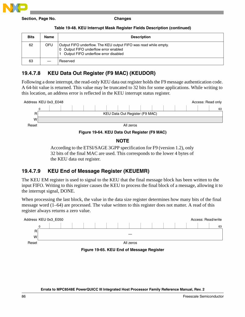
Section, Page No. Changes
Errata to MPC8548E PowerQUICC III Integrated Host Processor Family Reference Manual, Rev. 2
86 Freescale Semiconductor
19.4.7.8 KEU Data Out Register (F9 MAC) (KEUDOR)
Following a done interrupt, the read-only KEU data out register holds the F9 message authentication code. A 64-bit value is returned. This value may be truncated to 32 bits for some applications. While writing to this location, an address error is reflected in the KEU interrupt status register.
NOTEAccording to the ETSI/SAGE 3GPP specification for F9 (version 1.2), only 32 bits of the final MAC are used. This corresponds to the lower 4 bytes of the KEU data out register.
19.4.7.9 KEU End of Message Register (KEUEMR)
The KEU EM register is used to signal to the KEU that the final message block has been written to the input FIFO. Writing to this register causes the KEU to process the final block of a message, allowing it to the interrupt signal, DONE.
When processing the last block, the value in the data size register determines how many bits of the final message word (1–64) are processed. The value written to this register does not matter. A read of this register always returns a zero value.
62 OFU Output FIFO underflow. The KEU output FIFO was read while empty.0 Output FIFO underflow error enabled1 Output FIFO underflow error disabled
63 — Reserved
Address KEU 0x3_E048 Access: Read only
0 63
R KEU Data Out Register (F9 MAC)
W
Reset All zeros
Figure 19-64. KEU Data Out Register (F9 MAC)
Address KEU 0x3_E050 Access: Read/write
0 63
R—
W
Reset All zeros
Figure 19-65. KEU End of Message Register
Table 19-48. KEU Interrupt Mask Register Fields Description (continued)
Bits Name Description

Section, Page No. Changes
Errata to MPC8548E PowerQUICC III Integrated Host Processor Family Reference Manual, Rev. 2
Freescale Semiconductor 87
19.4.7.10 KEU IV_1 Register (KEUIV1)
The KEU IV_1 register is a general purpose IV register is used during the initialization phase of the F8 algorithms for 3GPP, GSM A5/3, EDGE A5/3, GPRS GEA3, and F9 algorithm for 3GPP. The appropriate value as defined by the standards for each algorithm must be written before a new message is started.
After the initialization phase has been completed, the KEU IV_1 register is no longer used for the remainder of F8 processing. However, if 3GPP F9 is selected because the KEU IV_1 register contains the direction bit as defined by the 3GPP standard, the KEU IV_1 register must be written back during context switches to complete the generation of the 3GPP MAC.
This table describes the KEU IV_1 register fields.
This figure shows how the KEU IV_1 register can be differentiated for different applications.
Figure 19-67. KEU IV_1 Application Field Comparison
Address KEU 0x3_E100 Access: Read/write
0 31 32 36 37 38 39 40 47 48 63
RCC CB CD 00 CA CE
W
Reset All zeros
Figure 19-66. KEU IV_1 Register
Table 19-49. KEU IV_1 Register Fields Description
Bits Field 3GPP DefinitionGSM - A5/3 Definition
EDGE - A5/3 Definition GPRS - GEA3 Definition
0–31 CC Count Count 0000000000 | | Count Frame dependent input value (32-bits)
32–36 CB Bearer 00000 00000 00000
37 CD Direction bit 0 0 0
38–39 0 00 00 00 00
40–47 CA 00000000 00001111 11110000 11111111
48–63 CE 000000000000000 0000000000000000 0000000000000000 0000000000000000
0 31 32 36 37 38 39 40 47 48 63
3GPP(F8)
Count Bearer Dir. 00 00000000 000000000000000
GSM(A5/3)
Count 00000 0 00 00001111 000000000000000
EDGE(A5/3)
0000000000 || Count 00000 0 00 11110000 000000000000000
GPRS(GEA3)
32 bit Frame Dependent Input Value
00000 0 00 11111111 000000000000000

Section, Page No. Changes
Errata to MPC8548E PowerQUICC III Integrated Host Processor Family Reference Manual, Rev. 2
88 Freescale Semiconductor
NOTEIt is the responsibility of the user to ensure that fields of the KEU IV_1 register are programmed correctly in accordance with the algorithm selected.
19.4.7.11 KEU ICV_In Register (KEUICV)
If ICV checking is required, then the value to be compared with the computed F9 MAC value must be written to the KEU ICV_In register before data size is written. As the KEU ICV_In register is in between IV_1 and IV_2, any descriptor operation that loads IV_2 must also load ICV_In. If CICV = 0, the ICV_In register should be loaded with 0x0000_0000_0000_0000.
19.4.7.12 KEU IV_2 Register (Fresh) (KEUIV2)
The KEU IV_2 register, shown in Figure 19-68, holds the F9 value, Fresh, which is used during the initialization phase of the 3GPP F9 algorithm. This value is ignored when the F8 algorithm is selected. The Fresh value must be written to bits 0:31 of the KEU IV_2 register before a new message to be processed with 3GPP F9 is started. After the initialization phase has been completed, the KEU IV_2 register is no longer used during message processing. The KEU IV_2 register need not be written during context switches.
19.4.7.13 KEU Context Data Registers (KEUCn)
The KEU includes six 64-bit KEU context data registers that store the running context used to process a message. The KEU context data registers must be read when changing context and are restored to their original values to resume processing of a partial message. For F8 and 3GPP F9 modes, all 64-bit KEU context data registers must be read to retrieve context, and all six registers must be written back to restore context. The context must be written prior to the key data. If the any of the KEU context data registers are written during message processing, a context error is generated. All KEU context data registers are cleared when a hard/soft reset or initialization is performed.
NOTEFor descriptor operation, if the entire context is unloaded for later reuse, the context data size must be 72 bytes, and the output will consist of KEU IV_1, KEU ICV_In, KEU IV_2, and six KEU context data registers. For operations performing processing of partial messages, if the context is unloaded, the PE bit in the KEU mode register must not be set. Also, for partial message processing, if the context is reloaded, the INT bit in the KEU mode register must not be set.
Address 0x3_E110 Access: Read/write
0 31 32 63
RFresh —
W
Reset All zeros
Figure 19-68. KEU IV_2 Register (Fresh)

Section, Page No. Changes
Errata to MPC8548E PowerQUICC III Integrated Host Processor Family Reference Manual, Rev. 2
Freescale Semiconductor 89
19.4.7.14 KEU Key Data Registers_1 and _2 (Confidentiality Key) (KEUKDn)
The first two KEU key data registers together hold one 128-bit key that is used for F8 encryption/decryption. The KEU key data register_1, (CK-high), holds the first 8 bytes (1–8). The KEU key data register_2, (CK-low), holds the second 8 bytes (9–16). The KEU key data registers must be written before message processing begins and cannot be written while the block is processing data, or else a context error occurs. While reading from either of these registers, an address error is reflected in the KEU interrupt status register.
19.4.7.15 KEU Key Data Registers _3 and _4 (Integrity Key) (KEUKDn)
The third and fourth KEU key data registers together hold one 128-bit key that is used for F9 message authentication. The KEU key data register_3, (IK-high), holds the first 8 bytes (1–8). The KEU key data register_4, (IK-low), holds the second 8 bytes (9–16). The KEU key data registers must be written before message processing begins and cannot be written while the block is processing data, or else, a context error occurs.
If the mode, F9 only, is set, the integrity key data may be optionally written to the KEU key data registers_1 and KEU key data registers_2. This eliminates the need for the host to offset from the base key address to write to the KEU key data registers_3 and KEU key data registers_4 while using the KEU exclusively for the F9 integrity function.
While reading from either of these registers, an address error is reflected in the KEU interrupt status register.
Address KEU 0x3_E400 Access: Read only
0 63
R KEU Key Data Register _1 (CK-high)
W
Reset All zeros
Figure 19-69. KEU Key Data Register_1 (CK-high)
Address KEU 0x3_E408 Access: Read only
0 63
R KEU Key Data Register _2 (CK-low)
W
Reset All zeros
Figure 19-70. KEU Key Data Register_2 (CK-Low)
Address KEU 0x3_E410 Access: Read only
0 63
R KEU Key Data Register _3 (IK-high)
W
Reset All zeros
Figure 19-71. KEU Key Data Register_3 (IK-high)

Section, Page No. Changes
Errata to MPC8548E PowerQUICC III Integrated Host Processor Family Reference Manual, Rev. 2
90 Freescale Semiconductor
19.4.7.16 KEU FIFOs
The KEU uses an input FIFO/output FIFO pair to hold data before and after the encryption process. Normally, the channels control all access to these FIFOs. For host-controlled operation, a write to anywhere in the KEU FIFO address space en-queues data to the KEU input FIFO, and a read from anywhere in the KEU FIFO address space de-queues data from the KEU output FIFO.
A write to the input FIFO go first to a staging register, which can be written by byte, word (4 bytes), or dword (8 bytes). When all 8 bytes of the staging register have been written, the entire dword is automatically en-queued into the FIFO. If any byte is written twice between en-queues, it causes an error interrupt of type AE from the EU. When writing the last portion of data, it is not necessary to write all 8 bytes. The last bytes remaining in the staging register are automatically padded with zeros and forced into the input FIFO when the KEU end of message register is written.
The output FIFO is readable by byte, word, or dword. When all 8 bytes of the head dword are read, the dword is automatically de-queued from the FIFO so that the next dword (if any) becomes available for reading. If any byte is read twice between de-queues, it causes an error interrupt of type AE from the EU.
The overflows and underflows caused by reading or writing the KEU FIFOs are reflected in the KEU interrupt status register.
The KEU fetches data 64 bits at a time from the KEU Input FIFO. During F8 processing, the input data is XORed with the generated keystream and the results are placed in the KEU output FIFO. During F9 processing, the input data is hashed with the integrity key and the resulting MAC is placed in the KEU data out register. The output size is the same as the input size.
20.4.1.1, 20-5 In Figure 20-1, “PORPLL Status Register (PORPLLSR),” change reset value for bits 8–9 to from “00” to “01,” as follows:
20.4.1.4, 20-8 In Table 20-4, “PORDEVSR Field Descriptions,” remove “or below” from PCI1_SPD (bit 16) field description.
Address KEU 0x3_E418 Access: Read only
0 63
R KEU Key Data Register _4 (IK-low)
W
Reset All zeros
Figure 19-72. KEU Key Data Register_4 (IK-low)
Offset 0xE_0000 Access: Read Only
0 9 10 15 16 17 18 25 26 30 31
R — e500_Ratio PCI1_clk_sel PCI2_clk_sel — Plat_Ratio 0
W
Reset 0 0 0 0 0 0 0 0 0 1 n n n n n n n n 0 0 0 0 0 0 0 0 n n n n n n
Figure 20-1. POR PLL Status Register (PORPLLSR)

Section, Page No. Changes
Errata to MPC8548E PowerQUICC III Integrated Host Processor Family Reference Manual, Rev. 2
Freescale Semiconductor 91
20.4.1.4, 20-9 In Table 20-7, “PORDEVSR Field Descriptions,” replace field descriptions of PCI1_SPD and PCI2_SPD with the following:
20.4.1.6, 20-11 In Figure 20-6, “POR Device Status Register 2 (PORDEVSR2),” modify reset value so that all bits are set to “n,” except for bit 29 (SRDS_EN). In other words, the reset value is 0xnnnn_nnn4.
20.4.1.15, 20-20 Update descriptions of some fields in Table 20-18, “RSTRSCR Field Descriptions,” as follows:Bits FieldDescription8 SRIO_RR Serial RapidIO (SRIO) reset requested10 BS_RR Boot sequence reset requested11 WDT_RR Watchdog timer reset requested12S W_RR Software settable reset requested (See Section 20.4.1.18, “Reset Control Register (RSTCR).”)
20.4.1.23, 20-26 In Table 20-26, “CLKOCR Field Descriptions,” modify CLKSEL (bits 26–31) field description by removing “Logic 0” and “Logic 1” configuration options.
20.4.1.24, 20-27 In Table 20-27, “SRDSCR0 Field Descriptions,” for both SRDSCR0[XMITEQ03] and SRDSCR0[XMITEQ47], the default value for PCI Express should be 1100 instead of 0100.
20.4.1.25, 20-27 Add field SRDSCR1[LBSELTYPE] in Figure 20-25, “SerDes Control Register 1 (SRDSCR1),” and its corresponding field description in Table 20-28, “SRDSCR1 Field Descriptions.” The register figure and field description table changes should appear as follows:
Table 20-7. PORDEVSR Field Descriptions
Bits Name Description
16 PCI1_SPD PCI1/PCI-X speed (See Section 4.4.3.18, ‘PCI Speed Configuration.”)0 PCI1/PCI-X set for low speed operation—PCI at or below 33MHz or PCI-X at or below 66.66 MHz1 PCI1/PCI-X set for normal speed operation—PCI above 33MHz, or PCI-X above 66.66 MHz
17 PCI2_SPD PCI2 speed (See Section 4.4.3.18, ‘PCI Speed Configuration.”)0 PCI2 set for low speed operation—at or below 33.33 MHz1 PCI2 set for normal speed operation—above 33.33 MHz
Offset 0xE_0F08 Access: Read/Write
0 1 2 3 4 5 6 7 8 20 21 24 25 31
RPD0 PD1 PD2 PD3 PD4 PD5 PD6 PD7 — LBSELTYPE —
W
Reset All zeros
Figure 20-25. SerDes Control Register 1 (SRDSCR1)

Section, Page No. Changes
Errata to MPC8548E PowerQUICC III Integrated Host Processor Family Reference Manual, Rev. 2
92 Freescale Semiconductor
20.4.1.26, 20-29 In Table 20-29, “TSEC12IOOVCR Field Descriptions,” add note to the REC_ADJ (bits 1–4) field description clarifying that this value may only be manually changed for TBI mode, as follows:“Note that manually changing this field from the default protocol-defined voltage value (automatically determined during POR protocol selection) is only supported for TBI mode.”
20.4.1.27, 20-29 In Table 20-30, “TSEC34IOOVC Field descriptions,” add note to the REC_ADJ (bits 1–4) field description clarifying that this value may only be manually changed for TBI mode, as follows:“Note that manually changing this field from the default protocol-defined voltage value (automatically determined during POR protocol selection) is only supported for TBI mode.”
21.4.7, 21-19 Add the following note, which applies to PCI/PCI-X 1 and PCI 2 events, to Table 21-10, “Performance Monitor Events”:“Note that PCI performance monitor event counts are only accurate when PCI is configured for synchronous operation.”
21.4.7, 21-27 In Table 21-10, “Performance Monitor Events,” update event Ref:25 (L2 cache) to read as follows: “L2 allocations based on core-initiated accesses. The data may come from any source.”
22.2.1, 22-6 In Table 22-2, “Debug, Watchpoint and Test Signal Summary,” modified function of TCK row to say “Clock for JTAG testing.”
22.3.1.2, 22-13 Add new section containing register WMAHR, as follows:
22.3.1.2 Watchpoint Monitor Address High Register (WMAHR)
The watchpoint monitor address high register (WMAHR), shown in Figure 22-4, contains the high-order address bits of the address to match against if WMCR[AMD] is clear.
Table 20-28. SRDSCR1 Field Descriptions
Bits Name Description
21–24 LBSELTYPE Select loop-back type0000 Application mode0001 Digital loopback mode0010–1111 Reserved
Offset 0xE_2008 Access: Read/Write
0 27 28 31
R— WMAH
W
Reset All zeros
Figure 22-4. Watchpoint Monitor Address High Register (WMAHR)
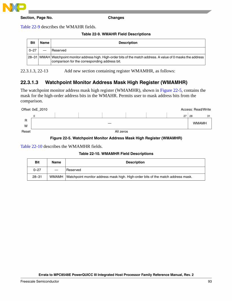
Section, Page No. Changes
Errata to MPC8548E PowerQUICC III Integrated Host Processor Family Reference Manual, Rev. 2
Freescale Semiconductor 93
Table 22-9 describes the WMAHR fields.
22.3.1.3, 22-13 Add new section containing register WMAMHR, as follows:
22.3.1.3 Watchpoint Monitor Address Mask High Register (WMAMHR)
The watchpoint monitor address mask high register (WMAMHR), shown in Figure 22-5, contains the mask for the high-order address bits in the WMAHR. Permits user to mask address bits from the comparison.
Table 22-10 describes the WMAMHR fields.
Table 22-9. WMAHR Field Descriptions
Bit Name Description
0–27 — Reserved
28–31 WMAH Watchpoint monitor address high. High-order bits of the match address. A value of 0 masks the address comparison for the corresponding address bit.
Offset 0xE_2010 Access: Read/Write
0 27 28 31
R— WMAMH
W
Reset All zeros
Figure 22-5. Watchpoint Monitor Address Mask High Register (WMAMHR)
Table 22-10. WMAMHR Field Descriptions
Bit Name Description
0–27 — Reserved
28–31 WMAMH Watchpoint monitor address mask high. High-order bits of the match address mask.

Document Number: MPC8548ERMADRev. 2.404/2013
Information in this document is provided solely to enable system and software
implementers to use Freescale products. There are no express or implied copyright
licenses granted hereunder to design or fabricate any integrated circuits based on the
information in this document.
Freescale reserves the right to make changes without further notice to any products
herein. Freescale makes no warranty, representation, or guarantee regarding the
suitability of its products for any particular purpose, nor does Freescale assume any
liability arising out of the application or use of any product or circuit, and specifically
disclaims any and all liability, including without limitation consequential or incidental
damages. “Typical” parameters that may be provided in Freescale data sheets and/or
specifications can and do vary in different applications, and actual performance may
vary over time. All operating parameters, including “typicals,” must be validated for each
customer application by customer’s technical experts. Freescale does not convey any
license under its patent rights nor the rights of others. Freescale sells products
pursuant to standard terms and conditions of sale, which can be found at the following
address: freescale.com/SalesTermsandConditions.
How to Reach Us:
Home Page: freescale.com
Web Support: freescale.com/support
Freescale, the Freescale logo, AltiVec, C-5, CodeTest, CodeWarrior, ColdFire, C-Ware, Energy Efficient Solutions logo, Kinetis, mobileGT, PowerQUICC, Processor Expert, QorIQ, Qorivva, StarCore, Symphony, and VortiQa are trademarks of Freescale Semiconductor, Inc., Reg. U.S. Pat. & Tm. Off. Airfast, BeeKit, BeeStack, ColdFire+, CoreNet, Flexis, MagniV, MXC, Platform in a Package, QorIQ Qonverge, QUICC Engine, Ready Play, SafeAssure, SMARTMOS, TurboLink, Vybrid, and Xtrinsic are trademarks of Freescale Semiconductor, Inc. All other product or service names are the property of their respective owners. The Power Architecture and Power.org word marks and the Power and Power.org logos and related marks are trademarks and service marks licensed by Power.org. © 2010-2013 Freescale Semiconductor, Inc.