
MPC8314E PowerQUICC II Pro Processor Hardware ...MPC8314E PowerQUICC II Pro Processor Hardware...
101
© Freescale Semiconductor, Inc., 2011. All rights reserved. Freescale Semiconductor Data Sheet: Technical Data This document provides an overview of the MPC8314E PowerQUICC™ II Pro processor features, including a block diagram showing the major functional components. The MPC8314E contains a core built on Power Architecture™ technology. It is a cost-effective, low-power, highly integrated host processor that addresses the requirements of several storage, consumer, and industrial applications, including main CPUs and I/O processors in network attached storage (NAS), voice over IP (VoIP) router/gateway, intelligent wireless LAN (WLAN), set top boxes, industrial controllers, and wireless access points. The MPC8314E extends the PowerQUICC II Pro family, adding higher CPU performance, new functionality, and faster interfaces while addressing the requirements related to time-to-market, price, power consumption, and package size. Note that while the MPC8314E supports a security engine, the MPC8314 does not. Document Number: MPC8314EEC Rev. 2, 11/2011 Contents 1. Overview . . . . . . . . . . . . . . . . . . . . . . . . . . . . . . . . . . . 2 2. MPC8314E Features . . . . . . . . . . . . . . . . . . . . . . . . . . 2 3. Electrical Characteristics . . . . . . . . . . . . . . . . . . . . . . 7 4. Power Characteristics . . . . . . . . . . . . . . . . . . . . . . . . 12 5. Clock Input Timing . . . . . . . . . . . . . . . . . . . . . . . . . . 13 6. RESET Initialization . . . . . . . . . . . . . . . . . . . . . . . . . 15 7. DDR and DDR2 SDRAM . . . . . . . . . . . . . . . . . . . . . 16 8. DUART . . . . . . . . . . . . . . . . . . . . . . . . . . . . . . . . . . . 22 9. Ethernet: Three-Speed Ethernet, MII Management . 22 10. USB . . . . . . . . . . . . . . . . . . . . . . . . . . . . . . . . . . . . . . 37 11. Local Bus . . . . . . . . . . . . . . . . . . . . . . . . . . . . . . . . . 39 12. JTAG . . . . . . . . . . . . . . . . . . . . . . . . . . . . . . . . . . . . . 42 13. I 2 C . . . . . . . . . . . . . . . . . . . . . . . . . . . . . . . . . . . . . . . 45 14. PCI . . . . . . . . . . . . . . . . . . . . . . . . . . . . . . . . . . . . . . 47 15. High-Speed Serial Interfaces (HSSI) . . . . . . . . . . . . 49 16. PCI Express . . . . . . . . . . . . . . . . . . . . . . . . . . . . . . . . 59 17. Timers . . . . . . . . . . . . . . . . . . . . . . . . . . . . . . . . . . . . 66 18. GPIO . . . . . . . . . . . . . . . . . . . . . . . . . . . . . . . . . . . . . 67 19. IPIC . . . . . . . . . . . . . . . . . . . . . . . . . . . . . . . . . . . . . . 68 20. SPI . . . . . . . . . . . . . . . . . . . . . . . . . . . . . . . . . . . . . . . 68 21. TDM . . . . . . . . . . . . . . . . . . . . . . . . . . . . . . . . . . . . . 70 22. Package and Pin Listings . . . . . . . . . . . . . . . . . . . . . 72 23. Clocking . . . . . . . . . . . . . . . . . . . . . . . . . . . . . . . . . . 85 24. Thermal . . . . . . . . . . . . . . . . . . . . . . . . . . . . . . . . . . . 90 25. System Design Information . . . . . . . . . . . . . . . . . . . 95 26. Ordering Information . . . . . . . . . . . . . . . . . . . . . . . . 98 27. Revision History . . . . . . . . . . . . . . . . . . . . . . . . . . . 100 MPC8314E PowerQUICC II Pro Processor Hardware Specifications
Transcript of MPC8314E PowerQUICC II Pro Processor Hardware ...MPC8314E PowerQUICC II Pro Processor Hardware...

© Freescale Semiconductor, Inc., 2011. All rights reserved.
Freescale SemiconductorData Sheet: Technical Data
This document provides an overview of the MPC8314E PowerQUICC™ II Pro processor features, including a block diagram showing the major functional components. The MPC8314E contains a core built on Power Architecture™ technology. It is a cost-effective, low-power, highly integrated host processor that addresses the requirements of several storage, consumer, and industrial applications, including main CPUs and I/O processors in network attached storage (NAS), voice over IP (VoIP) router/gateway, intelligent wireless LAN (WLAN), set top boxes, industrial controllers, and wireless access points. The MPC8314E extends the PowerQUICC II Pro family, adding higher CPU performance, new functionality, and faster interfaces while addressing the requirements related to time-to-market, price, power consumption, and package size. Note that while the MPC8314E supports a security engine, the MPC8314 does not.
Document Number: MPC8314EECRev. 2, 11/2011
Contents1. Overview . . . . . . . . . . . . . . . . . . . . . . . . . . . . . . . . . . . 22. MPC8314E Features . . . . . . . . . . . . . . . . . . . . . . . . . . 23. Electrical Characteristics . . . . . . . . . . . . . . . . . . . . . . 74. Power Characteristics . . . . . . . . . . . . . . . . . . . . . . . . 125. Clock Input Timing . . . . . . . . . . . . . . . . . . . . . . . . . . 136. RESET Initialization . . . . . . . . . . . . . . . . . . . . . . . . . 157. DDR and DDR2 SDRAM . . . . . . . . . . . . . . . . . . . . . 168. DUART . . . . . . . . . . . . . . . . . . . . . . . . . . . . . . . . . . . 229. Ethernet: Three-Speed Ethernet, MII Management . 22
10. USB . . . . . . . . . . . . . . . . . . . . . . . . . . . . . . . . . . . . . . 3711. Local Bus . . . . . . . . . . . . . . . . . . . . . . . . . . . . . . . . . 3912. JTAG . . . . . . . . . . . . . . . . . . . . . . . . . . . . . . . . . . . . . 4213. I2C . . . . . . . . . . . . . . . . . . . . . . . . . . . . . . . . . . . . . . . 4514. PCI . . . . . . . . . . . . . . . . . . . . . . . . . . . . . . . . . . . . . . 4715. High-Speed Serial Interfaces (HSSI) . . . . . . . . . . . . 4916. PCI Express . . . . . . . . . . . . . . . . . . . . . . . . . . . . . . . . 5917. Timers . . . . . . . . . . . . . . . . . . . . . . . . . . . . . . . . . . . . 6618. GPIO . . . . . . . . . . . . . . . . . . . . . . . . . . . . . . . . . . . . . 6719. IPIC . . . . . . . . . . . . . . . . . . . . . . . . . . . . . . . . . . . . . . 6820. SPI . . . . . . . . . . . . . . . . . . . . . . . . . . . . . . . . . . . . . . . 6821. TDM . . . . . . . . . . . . . . . . . . . . . . . . . . . . . . . . . . . . . 7022. Package and Pin Listings . . . . . . . . . . . . . . . . . . . . . 7223. Clocking . . . . . . . . . . . . . . . . . . . . . . . . . . . . . . . . . . 8524. Thermal . . . . . . . . . . . . . . . . . . . . . . . . . . . . . . . . . . . 9025. System Design Information . . . . . . . . . . . . . . . . . . . 9526. Ordering Information . . . . . . . . . . . . . . . . . . . . . . . . 9827. Revision History . . . . . . . . . . . . . . . . . . . . . . . . . . . 100
MPC8314E PowerQUICC II Pro Processor Hardware Specifications

MPC8314E PowerQUICC II Pro Processor Hardware Specifications, Rev. 2
2 Freescale Semiconductor
Overview
1 OverviewThe MPC8314E incorporates the e300c3 (MPC603e-based) core, which includes 16 Kbytes of L1 instruction and data caches, on-chip memory management units (MMUs), and floating-point support. In addition to the e300 core, the SoC platform includes features such as dual enhanced three-speed 10, 100, 1000 Mbps Ethernet controllers (eTSECs) with SGMII support, a 32- or 16-bit DDR1/DDR2 SDRAM memory controller, a security engine to accelerate control and data plane security protocols, and a high degree of software compatibility with previous-generation PowerQUICC processor-based designs for backward compatibility and easier software migration. The MPC8314E also offers peripheral interfaces such as a 32-bit PCI interface with up to 66 MHz operation, 16-bit enhanced local bus interface with up to 66 MHz operation, TDM interface, and USB 2.0 with an on-chip USB 2.0 PHY.
8314E offers additional high-speed interconnect support with dual single-lane PCI Express interfaces. When not used for PCI Express, the SerDes interface may be configured to support SGMII. The MPC8314E security engine (SEC 3.3) allows CPU-intensive cryptographic operations to be offloaded from the main CPU core. This figure shows a block diagram of the MPC8314E.
Figure 1. MPC8314E Block Diagram
2 MPC8314E FeaturesThe following features are supported in the MPC8314E.
2.1 e300 CoreThe e300 core has the following features:
• Operates at up to 400 MHz
• 16-Kbyte instruction cache, 16-Kbyte data cache
eTSEC
RTBI, SGMII
DUART
InterruptI2C
Timers
GPIO
EnhancedDDR1/DDR2
ControllerController
PCI
I/OSequencer(IOS)
Security
Note: The MPC8314 do not include a security engine.
Local Bus,
USB 2.0 HSHost/Device/OTG
ULPI On-ChipHS PHY
SPIEngine 3.3
PCIExpress
x1
DMA
TDM
RGMII, (R)MII
eTSEC
RTBI, SGMIIRGMII, (R)MII
16-KBD-Cache
16-KBI-Cache
e300c3 Core withPower Management
FPU
PCIExpress
x1
MPC8314E
MPC8314E PowerQUICC II Pro Processor Hardware Specifications, Rev. 2
Freescale Semiconductor 3
MPC8314E Features
• One floating point unit and two integer units
• Software-compatible with the Freescale processor families implementing the PowerPC Architecture
• Performance monitor
2.2 Serial InterfacesThe following interfaces are supported in the MPC8314E.
• Two enhanced TSECs (eTSECs)
• Two Ethernet interfaces using one RGMII/MII/RMII/RTBI or SGMII (no GMII)
• Dual UART, one I2C, and one SPI interface
2.3 Security EngineThe security engine is optimized to handle all the algorithms associated with IPSec, 802.11i, and iSCSI. The security engine contains one crypto-channel, a controller, and a set of crypto execution units (EUs). The execution units are:
• Public key execution unit (PKEU)
— RSA and Diffie-Hellman (to 4096 bits)
— Programmable field size up to 2048 bits
— Elliptic curve cryptography (1023 bits)
— F2m and F(p) modes
— Programmable field size up to 511 bits
• Data encryption standard execution unit (DEU)
— DES, 3DES
— Two key (K1, K2) or three key (K1, K2, K3)
— ECB, CBC, CFB-64 and OFB-64 modes for both DES and 3DES
• Advanced encryption standard unit (AESU)
— Implements the Rinjdael symmetric key cipher
— Key lengths of 128, 192, and 256 bits
— ECB, CBC, CCM, CTR, GCM, CMAC, OFB, CFB, XCBC-MAC and LRW modes
— XOR acceleration
• Message digest execution unit (MDEU)
— SHA with 160-bit, 256-bit, 384-bit and 512-bit message digest
— SHA-384/512
— MD5 with 128-bit message digest
— HMAC with either algorithm
• Random number generator (RNG)

MPC8314E PowerQUICC II Pro Processor Hardware Specifications, Rev. 2
4 Freescale Semiconductor
MPC8314E Features
— Combines a True Random Number Generator (TRNG) and a NIST-approved Pseudo-Random Number Generator (PRNG) (as described in Annex C of FIPS140-2 and ANSI X9.62).
• Cyclical Redundancy Check Hardware Accelerator (CRCA)
— Implements CRC32C as required for iSCSI header and payload checksums, CRC32 as required for IEEE 802 packets, as well as for programmable 32 bit CRC polynomials
2.4 DDR Memory ControllerThe DDR1/DDR2 memory controller includes the following features:
• Single 16- or 32-bit interface supporting both DDR1 and DDR2 SDRAM
• Support for up to 266 MHz data rate
• Support for two physical banks (chip selects), each bank independently addressable
• 64-Mbit to 2-Gbit (for DDR1) and to 4-Gbit (for DDR2) devices with x8/x16 data ports (no direct x4 support)
• Support for one 16-bit device or two 8-bit devices on a 16-bit bus or two 16-bit devices on a 32-bit bus
• Support for up to 16 simultaneous open pages
• Supports auto refresh
• On-the-fly power management using CKE
• 1.8-/2.5-V SSTL2 compatible I/O
2.5 PCI ControllerThe PCI controller includes the following features:
• Designed to comply with PCI Local Bus Specification Revision 2.3
• Single 32-bit data PCI interface operates at up to 66 MHz
• PCI 3.3-V compatible (not 5-V compatible)
• Support for host and agent modes
• On-chip arbitration, supporting three external masters on PCI
• Selectable hardware-enforced coherency
2.6 TDM InterfaceThe TDM interface includes the following features:
• Independent receive and transmit with dedicated data, clock and frame sync line
• Separate or shared RCK and TCK whose source can be either internal or external
• Glueless interface to E1/T1 frames and MVIP, SCAS, and H.110 buses
• Up to 128 time slots, where each slot can be programmed to be active or inactive
• 8- or 16-bit word widths
• The TDM Transmitter Sync Signal (TFS), Transmitter Clock Signal (TCK) and Receiver Clock

MPC8314E PowerQUICC II Pro Processor Hardware Specifications, Rev. 2
Freescale Semiconductor 5
MPC8314E Features
• Signal (RCK) can be configured as either input or output
• Frame sync and data signals can be programmed to be sampled either on the rising edge or on the falling edge of the clock
• Frame sync can be programmed as active low or active high
• Selectable delay (0–3 bits) between the Frame Sync signal and the beginning of the frame
• MSB or LSB first support
2.7 USB Dual-Role ControllerThe USB controller includes the following features:
• Designed to comply with USB Specification, Rev. 2.0
• Supports operation as a stand-alone USB device
— Supports one upstream facing port
— Supports three programmable USB endpoints
• Supports operation as a stand-alone USB host controller
— Supports USB root hub with one downstream-facing port
— Enhanced host controller interface (EHCI) compatible
• Supports high-speed (480 Mbps), full-speed (12 Mbps), and low-speed (1.5 Mbps) operation. Low-speed operation is supported only in host mode.
• Supports UTMI+ low pin interface (ULPI) or on-chip USB-2.0 full-speed/high-speed PHY
• Supports USB on-the-go mode, which includes both device and host functionality, when using an external ULPI PHY
2.8 Dual PCI Express InterfacesThe PCI Express interfaces have the following features:
• PCI Express 1.0a compatible
• x1 link width
• Selectable operation as root complex or endpoint
• Both 32- and 64-bit addressing
• 128-byte maximum payload size
• Support for MSI and INTx interrupt messages
• Virtual channel 0 only
• Selectable Traffic Class
• Full 64-bit decode with 32-bit wide windows
• Dedicated descriptor based DMA engine per interface with separate read and write channels

MPC8314E PowerQUICC II Pro Processor Hardware Specifications, Rev. 2
6 Freescale Semiconductor
MPC8314E Features
2.9 Dual Enhanced Three-Speed Ethernet Controllers (eTSECs)The eTSECs include the following features:
• Two SGMII/RGMII/MII/RMII/RTBI interfaces
• Two controllers designed to comply with IEEE Std 802.3™, IEEE 802.3u™, IEEE 802.3x™, IEEE 802.3z™, IEEE 802.3au™, IEEE 802.3ab™, and IEEE Std 1588™
• Support for Wake-on-Magic Packet™, a method to bring the device from standby to full operating mode
• MII management interface for external PHY control and status.
2.10 Integrated Programmable Interrupt Controller (IPIC)The integrated programmable interrupt controller (IPIC) provides a flexible solution for general-purpose interrupt control. The IPIC programming model is compatible with the MPC8260 interrupt controller and supports external and internal discrete interrupt sources. Interrupts can also be redirected to an external interrupt controller.
2.11 Power Management Controller (PMC)The MPC8314E supports a range of power management states that significantly lower power consumption under the control of the power management controller. The PMC includes the following features:
• Provides power management when the device is used in both PCI host and agent modes
• PCI Power Management 1.2 D0, D1, D2, D3hot, and D3cold states
• PME generation in PCI agent mode, PME detection in PCI host mode
• Wake-up from Ethernet (magic packet), USB, GPIO, and PCI (PME input as host) while in the D1, D2 and D3hot states
• A new low-power standby power management state called D3warm
— The PMC, one Ethernet port, and the GTM block remain powered via a split power supply controlled through an external power switch
— Wake-up events include Ethernet (magic packet), GTM, GPIO, or IRQ inputs and cause the device to transition back to normal operation
— PCI agent mode is not be supported in D3warm state
• PCI Express-based PME events are not supported
2.12 Serial Peripheral Interface (SPI)The serial peripheral interface (SPI) allows the MPC8314E to exchange data between other PowerQUICC family chips, Ethernet PHYs for configuration, and peripheral devices such as EEPROMs, real-time clocks, A/D converters, and ISDN devices.
The SPI is a full-duplex, synchronous, character-oriented channel that supports a four-wire interface (receive, transmit, clock, and slave select). The SPI block consists of transmitter and receiver sections, an independent baud-rate generator, and a control unit.

MPC8314E PowerQUICC II Pro Processor Hardware Specifications, Rev. 2
Freescale Semiconductor 7
Electrical Characteristics
2.13 DMA Controller, I2C, DUART, Enhanced Local Bus Controller (eLBC), and Timers
The integrated four-channel DMA controller includes the following features:
• Allows chaining (both extended and direct) through local memory-mapped chain descriptors (accessible by local masters)
• Misaligned transfer capability for source/destination address
• Supports external DREQ, DACK and DONE signals
There is one I2C controller. This synchronous, multi-master buses can be connected to additional devices for expansion and system development.
The DUART supports full-duplex operation and is compatible with the PC16450 and PC16550 programming models. 16-byte FIFOs are supported for both the transmitter and the receiver.
The eLBC port allows connections with a wide variety of external DSPs and ASICs. Three separate state machines share the same external pins and can be programmed separately to access different types of devices. The general-purpose chip select machine (GPCM) controls accesses to asynchronous devices using a simple handshake protocol. The three user programmable machines (UPMs) can be programmed to interface to synchronous devices or custom ASIC interfaces. Each chip select can be configured so that the associated chip interface can be controlled by the GPCM or UPM controller. Both may exist in the same system. The local bus can operate at up to 66 MHz.
The system timers include the following features: periodic interrupt timer, real time clock, software watchdog timer, and two general-purpose timer blocks.
3 Electrical CharacteristicsThis section provides the AC and DC electrical specifications and thermal characteristics for the MPC8314E, which is currently targeted to these specifications. Some of these specifications are independent of the I/O cell, but they are included for complete reference. These are not purely I/O buffer design specifications.
3.1 Overall DC Electrical CharacteristicsThis section covers the ratings, conditions, and other characteristics.
3.1.1 Absolute Maximum Ratings
This table provides the absolute maximum ratings.
Table 1. Absolute Maximum Ratings 1
Characteristic Symbol Max Value Unit Note
Core supply voltage VDD –0.3 to 1.26 V —
PLL supply voltage AVDD –0.3 to 1.26 V —
DDR1 DRAM I/O supply voltage GVDD –0.3 to 2.7 V —

MPC8314E PowerQUICC II Pro Processor Hardware Specifications, Rev. 2
8 Freescale Semiconductor
Electrical Characteristics
DDR2 DRAM I/O supply voltage GVDD –0.3 to 1.9 V —
PCI, local bus, DUART, system control and power management, I2C, Ethernet management, 1588 timer and JTAG I/O voltage
NVDD –0.3 to 3.6 V 7
USB, and eTSEC I/O voltage LVDD –0.3 to 2.75 or–0.3 to 3.6
V 6, 8
PHY voltage USB PHY USB_PLL_PWR1 –0.3 to 1.26 V —
USB_PLL_PWR3, USB_VDDA_BIAS,
VDDA
–0.3 to 3.6 V —
SERDES PHY XCOREVDD, XPADVDD, SDAVDD
–0.3 to 1.26 V —
Input voltage DDR DRAM signals MVIN –0.3 to (GVDD + 0.3) V 2, 4
DDR DRAM reference MVREF –0.3 to (GVDD + 0.3) V 2, 4
eTSEC signals LVIN –0.3 to (LVDD + 0.3) V 3, 4
Local bus, DUART, SYS_CLK_IN, system control and power management, I2C, and JTAG signals
NVIN –0.3 to (NVDD + 0.3) V 3, 4
PCI NVIN –0.3 to (NVDD + 0.3) V 5
Storage temperature range TSTG –55 to150 C —
Note: 1. Functional and tested operating conditions are given in Table 2. Absolute maximum ratings are stress ratings only, and
functional operation at the maximums is not guaranteed. Stresses beyond those listed may affect device reliability or cause permanent damage to the device.
2. Caution: MVIN must not exceed GVDD by more than 0.3 V. This limit may be exceeded for a maximum of 20 ms during power-on reset and power-down sequences.
3. Caution: (N,L)VIN must not exceed (N,L)VDD by more than 0.3 V. This limit may be exceeded for a maximum of 20 ms during power-on reset and power-down sequences.
4. (M,N,L)VIN and MVREF may overshoot/undershoot to a voltage and for a maximum duration as shown in Figure 2. 5. NVIN on the PCI interface may overshoot/undershoot according to the PCI Electrical Specification for 3.3-V operation, as
shown in Figure 2. 6. The max value of supply voltage should be selected based on the RGMII mode.7. NVDD means NVDD1_OFF, NVDD1_ON, NVDD2_OFF, NVDD2_ON, NVDD3_OFF, NVDD4_OFF8. LVDD means LVDD1_OFF and LVDD2_ON
Table 1. Absolute Maximum Ratings 1 (continued)
Characteristic Symbol Max Value Unit Note

MPC8314E PowerQUICC II Pro Processor Hardware Specifications, Rev. 2
Freescale Semiconductor 9
Electrical Characteristics
3.1.2 Power Supply Voltage Specification
This table provides the recommended operating conditions for theMPC8314E. Note that the values in this table are the recommended and tested operating conditions. Proper device operation outside of these conditions is not guaranteed.
Table 2. Recommended Operating Conditions
Characteristic SymbolRecommended
Value1 UnitStatus in D3 Warm mode
Note
SerDes internal digital power XCOREVDD 1.0 ± 50 mv V Switched Off —
SerDes internal digital power XCOREVSS 0.0 V — —
SerDes I/O digital power XPADVDD 1.0 ± 50 mv V Switched Off —
SerDes I/O digital power XPADVSS 0.0 V — —
SerDes analog power for PLL SDAVDD 1.0 ± 50 mv V Switched Off —
SerDes analog power for PLL SDAVSS 0.0 V — —
Dedicated 3.3 V analog power for USB PLL USB_PLL_PWR3 3.3 ± 165mv V Switched Off —
Dedicated 1.0 Vanalog power for USB PLL USB_PLL_PWR1 1.0 ± 50 mv V Switched Off —
Dedicated analog ground for USB PLL USB_PLL_GND 0.0 V — —
Dedicated USB power for USB bias circuit USB_VDDA_BIAS 3.3 ± 300 mv V Switched Off —
Dedicated USB ground for USB bias circuit USB_VSSA_BIAS 0.0 V — —
Dedicated power for USB transceiver USB_VDDA 3.3 ± 300 mv V Switched Off —
Dedicated ground for USB transceiver USB_VSSA 0.0 V — —
Core supply voltage VDD 1.0 ± 50 mv V Switched Off —
Core supply voltage VDDC 1.0 ± 50 mv V Switched On —
Analog power for e300 core APLL AVDD1 1.0 ± 50 mv V Switched Off 6
Analog power for system APLL AVDD2 1.0 ± 50 mv V Switched On 6
DDR and DDR2 DRAM I/O voltage GVDD 2.5 ± 200 mv1.8 ± 100 mv
V Switched Off —
Differential reference voltage for DDR and DDR2 controller
MVREF GVDD /2 V Switched Off —
Standard I/O voltage NVDD1_ON 3.3 ± 300 mv V Switched On 1
Standard I/O voltage NVDD2_ON 3.3 ± 300 mv V Switched On 1
Standard I/O voltage NVDD1_OFF 3.3 ± 300 mv V Switched Off 2
Standard I/O voltage NVDD2_OFF 3.3 ± 300 mv V Switched Off 2
Standard I/O voltage NVDD3_OFF 3.3 ± 300 mv V Switched Off 2
Standard I/O voltage NVDD4_OFF 3.3 ± 300 mv V Switched Off 2
eTSEC/USBdr I/O supply LVDD1_OFF 2.5 ± 125 mv3.3 ± 300 mv
V Switched Off —
eTSEC I/O supply LVDD2_ON 2.5 ± 125 mv3.3 ± 300 mv
V Switched On —
Analog and digital ground VSS 0.0 V — —
Junction temperature range TA/TJ 0 to105 C — 3

MPC8314E PowerQUICC II Pro Processor Hardware Specifications, Rev. 2
10 Freescale Semiconductor
Electrical Characteristics
This figure shows the undershoot and overshoot voltages at the interfaces of the MPC8314E.
Figure 2. Overshoot/Undershoot Voltage for GVDD/NVDD/LVDD
3.1.3 Output Driver Characteristics
This table provides information on the characteristics of the output driver strengths. The values are preliminary estimates.
Note: 1. The NVDDx_ON are static power supplies and can be connected together.2. The NVDDx_OFF are switchable power supplies and can be connected together.3. Minimum Temperature is specified with TA;maximum temperature is specified with TJ.4. All Power rails must be connected and power applied to the MPC8314 even if the IP interfaces are not used.5. All I/O pins should be interfaced with peripherals operating at same voltage level.6. This voltage is the input to the filter discussed in Section 25.2, “PLL Power Supply Filtering” and not necessarily the voltage
at the AVDD pin.7. All 1V power supplies should be derived from the same source.
Table 3. Output Drive Capability
Driver TypeOutput
Impedance ()SupplyVoltage
Local bus interface utilities signals 42 NVDD = 3.3 V
PCI signals 25
DDR signal1 18 GVDD = 2.5 V
DDR2 signal 1 18 GVDD = 1.8 V
Table 2. Recommended Operating Conditions (continued)
Characteristic SymbolRecommended
Value1 UnitStatus in D3 Warm mode
Note
GNDGND – 0.3 V
GND – 0.7 VNot to Exceed 10%
G/L/NVDD + 20%
G/L/NVDD
G/L/NVDD + 5%
of tinterface1
1. tinterface refers to the clock period associated with the bus clock interface.
VIH
VIL
Note:

MPC8314E PowerQUICC II Pro Processor Hardware Specifications, Rev. 2
Freescale Semiconductor 11
Electrical Characteristics
3.2 Power SequencingThe MPC8314E does not require the core supply voltage (VDD and VDDC) and I/O supply voltages (GVDD, LVDDx_ON, LVDDx_OFF, NVDDx_ON and NVDDx_OFF) to be applied in any particular order. During the power ramp up, before the power supplies are stable, if the I/O voltages are supplied before the core voltage, there may be a period of time when all input and output pins be actively driven and cause contention and/or excessive current. In order to avoid actively driving the I/O pins and to eliminate excessive current draw, apply the continuous core voltage (VDDC) before the continuous I/O voltages (LVDDx_ON and NVDDx_ON) and switchable core voltage (VDD) before the switchable I/O voltages (GVDD, LVDDx_OFF, and NVDDx_OFF). PORESET should be asserted before the continuous power supplies fully ramp up. In the case where the core voltage is applied first, the core voltage supply must rise to 90% of its nominal value before the I/O supplies reach 0.7 V, see Figure 3. Once all the power supplies are stable, wait for a minimum of 32 clock cycles before negating PORESET.
The I/O power supply ramp-up slew rate should be slower than 4V/100 s, this requirement is for ESD circuit.
This figure shows the power-up sequencing for switchable and continuous supplies.
Figure 3. Power-Up Sequencing
When switching from normal mode to D3 warm (standby) mode, first turn off the switchable I/O voltage supply and then turn off the switchable core voltage supply. Similarly, when switching from D3 warm (standby) mode to normal mode, first turn on the switchable core voltage supply and then turn on the switchable I/O voltage supply.
DUART, system control, I2C, JTAG,SPI 42 NVDD = 3.3 V
GPIO signals 42 NVDD = 3.3 V
eTSEC 42 LVDD = 3.3 V / 2.5 V
1 Output Impedance can also be adjusted through configurable options in DDR Control Driver Register (DDRCDR). See the MPC8315E PowerQUICC II Pro Integrated Host Processor Family Reference Manual.
Table 3. Output Drive Capability (continued)
Driver TypeOutput
Impedance ()SupplyVoltage
Continuous I/O Voltage
Continuous Core Voltage
0.7 V90%
t
V Switchable I/O Voltage
Switchable Core Voltage (VDD)
0.7 V90%
t
V
Power sequence for continuous power supplies Power sequence for switchable power supplies

MPC8314E PowerQUICC II Pro Processor Hardware Specifications, Rev. 2
12 Freescale Semiconductor
Power Characteristics
CAUTIONWhen the device is in D3 warm (standby) mode, all external voltage supplies applied to any I/O pins, with the exception of wake-up pins, must be turned off. Applying supplied external voltage to any I/O pins, except the wake up pins, while the device is in D3 warm standby mode may cause permanent damage to the device.
An example of the power-up sequence is shown in Figure 4 when implemented along with low power D3 warm mode.
Figure 4. Power Up Sequencing Example with Low power D3 Warm Mode
4 Power CharacteristicsThis table shows the estimated typical power dissipation for this family of devices.
Table 4. MPC8314E Power Dissipation(Does not include I/O power dissipation)
Core Frequency (MHz) CSB Frequency (MHz) Typical 1,3 Maximum 1,2 Unit
266 133 1.116 1.646 W
333 133 1.142 1.665 W
400 133 1.167 1.690 W
Note: 1. The values do not include I/O supply power, but do include core, AVDD, USB PLL, and digital SerDes power.2. Maximum power is based on a voltage of Vdd = 1.05V, a junction temperature of Tj = 105°C, and an artificial
smoker test.3. Typical power is based on a voltage of Vdd = 1.05V, and an artificial smoker test running at room temperature.
Continuous I/O Voltage
Continuous Core Voltage
90%
PORESET
tSYS_CLK_IN / tPCI_SYNC_IN >= 32 clock
t
V
Switchable Core Voltage
Switchable I/O Voltage
(LVDDx_ON, NVDDx_ON) (GVDD, LVDDx_OFF, NVDDx_OFF)
VDDC (VDD)
0

MPC8314E PowerQUICC II Pro Processor Hardware Specifications, Rev. 2
Freescale Semiconductor 13
Clock Input Timing
This table shows the estimated typical I/O power dissipation for this family of devices.
5 Clock Input TimingThis section provides the clock input DC and AC electrical characteristics for the MPC8314E.
Table 5. MPC8314E Power Dissipation
Interface FrequencyGVDD(1.8 V)
GVDD(2.5 V)
NVDD(3.3 V)
LVDD1_OFF/LVDD2_ON
(3.3V)
LVDD2_ON
(3.3V)
VDD33PLL, VDD33ANA
(3.3V)
SATA_VDD, VDD1IO,
VDD1ANA(1.0V)
XCOREVDD, XPADVDD, SDAVDD
(1.0V)
Unit
DDR 1Rs = 22Rt = 50
266MHz, 32 bits
— 0.323 — — — — — — W
200MHz, 32 bits
— 0.291 — — — — — — W
DDR 2Rs = 22Rt = 75
266MHz, 32 bits
0.246 — — — — — — — W
200MHz, 32bits
0.225 — — — — — — — W
PCI I/O load = 50pF
33 MHz — — 0.120 — — — — — W
66 MHz — — 0.249 — — — — — W
Local bus I/O load = 20pF
66 MHz — — — — 0.056 — — — W
50 MHz — — — — 0.040 — — — W
eTSEC I/O load = 20pFMultiple by number of interface
used
MII, 25MHz — — — 0.008 — — — — W
RGMII, 125MHz(3.3V)
— — — 0.078 — — — — W
RGMII, 125MHz(2.5V)
— — — 0.044 — — — — W
USBDR Controller
(ULPI mode) load =20pF
60 MHz — — — 0.078 — — — — W
USBDR+ Internal PHY (UTMI mode)
480 MHz — — — 0.274 — — — — W
PCI Express two x1lane
2.5 GHz — — — — — — — 0.190 W
Other I/O — — — 0.015 — — — — — W

MPC8314E PowerQUICC II Pro Processor Hardware Specifications, Rev. 2
14 Freescale Semiconductor
Clock Input Timing
5.1 DC Electrical CharacteristicsThis table provides the clock input (SYS_CLK_IN/PCI_SYNC_IN) DC timing specifications for the MPC8314E.
5.2 AC Electrical CharacteristicsThe primary clock source for the MPC8314E can be one of two inputs, SYS_CLK_IN or PCI_CLK, depending on whether the device is configured in PCI host or PCI agent mode. This table provides the clock input (SYS_CLK_IN/PCI_CLK) AC timing specifications for the MPC8314E.
Table 6. SYS_CLK_IN DC Electrical Characteristics
Parameter Condition Symbol Min Max Unit
Input high voltage — VIH 2.4 NVDD + 0.3 V
Input low voltage — VIL -0.3 0.4 V
SYS_CLK_IN input current 0 V VIN NVDD IIN — ±10 A
SYS_XTAL_IN input current 0 V VIN NVDD IIN — ±40 A
PCI_SYNC_IN input current 0 V VIN NVDD IIN — ±10 A
RTC_CLK input current 0 V VIN NVDD IIN — ±10 A
USB_CLK_IN input current 0 V VIN NVDD IIN — ±10 A
USB_XTAL_IN input current 0 V VIN NVDD IIN — ±40 A
Table 7. SYS_CLK_IN AC Timing Specifications
Parameter/Condition Symbol Min Typical Max Unit Note
SYS_CLK_IN/PCI_CLK frequency fSYS_CLK_IN 24 — 66.67 MHz 1, 6, 7
SYS_CLK_IN/PCI_CLK cycle time tSYS_CLK_IN 15 — 41.6 ns 6
SYS_CLK_IN rise and fall time tKH, tKL 0.6 — 4 ns 2, 6
PCI_CLK rise and fall time tPCH, tPCL 0.6 0.8 1.2 ns 2
SYS_CLK_IN/PCI_CLK duty cycle tKHK/tSYS_CLK_IN 40 — 60 % 3, 6
SYS_CLK_IN/PCI_CLK jitter — — — ±150 ps 4, 5, 6
Note: 1. Caution: The system, core, and security block must not exceed their respective maximum or minimum operating
frequencies. 2. Rise and fall times for SYS_CLK_IN/PCI_CLK are specified at 20% to 80% of signal swing.3. Timing is guaranteed by design and characterization.4. This represents the total input jitter—short term and long term—and is guaranteed by design.5. The SYS_CLK_IN/PCI_CLK driver’s closed loop jitter bandwidth should be <500 kHz at –20 dB. The bandwidth must be set
low to allow cascade-connected PLL-based devices to track SYS_CLK_IN drivers with the specified jitter.6. The parameter names PCI_CLK and PCI_SYNC_IN are used interchangeably in this document.7. Spread spectrum is allowed up to 1% down-spread at 33kHz.(max. rate).

MPC8314E PowerQUICC II Pro Processor Hardware Specifications, Rev. 2
Freescale Semiconductor 15
RESET Initialization
6 RESET InitializationThis section describes the DC and AC electrical specifications for the reset initialization timing and electrical requirements of the MPC8314E.
6.1 RESET DC Electrical CharacteristicsThis table provides the DC electrical characteristics for the RESET pins of the MPC8314E.
6.2 RESET AC Electrical CharacteristicsThis table provides the reset initialization AC timing specifications of the MPC8314E.
Table 8. RESET Pins DC Electrical Characteristics
Characteristic Symbol Condition Min Max Unit
Input high voltage VIH — 2.0 NVDD + 0.3 V
Input low voltage VIL — –0.3 0.8 V
Input current IIN 0 V VIN NVDD — ±5 A
Output high voltage VOH IOH = –8.0 mA 2.4 — V
Output low voltage VOL IOL = 8.0 mA — 0.5 V
Output low voltage VOL IOL = 3.2 mA — 0.4 V
Table 9. RESET Initialization Timing Specifications
Parameter/Condition Min Max Unit Note
Required assertion time of HRESET to activate reset flow 32 — tPCI_SYNC_IN 1
Required assertion time of PORESET with stable clock applied to SYS_CLK_IN when the device is in PCI host mode
32 — tSYS_CLK_IN 2
Required assertion time of PORESET with stable clock applied to PCI_SYNC_IN when the device is in PCI agent mode
32 — tPCI_SYNC_IN 1
HRESET assertion (output) 512 — tPCI_SYNC_IN 1
Input setup time for POR configuration signals (CFG_RESET_SOURCE[0:3] and CFG_SYS_CLKIN_DIV) with respect to negation of PORESET when the device is in PCI host mode
4 — tSYS_CLK_IN 2, 4
Input setup time for POR configuration signals (CFG_RESET_SOURCE[0:3] and CFG_SYS_CLKIN_DIV) with respect to negation of PORESET when the device is in PCI agent mode
4 — tPCI_SYNC_IN 1
Input hold time for POR configuration signals with respect to negation of HRESET 0 — ns —
Time for the device to turn off POR configuration signals with respect to the assertion of HRESET
— 4 ns 3
Time for the device to turn on POR config signals with respect to the negation of HRESET
1 — tPCI_SYNC_IN 1, 3

MPC8314E PowerQUICC II Pro Processor Hardware Specifications, Rev. 2
16 Freescale Semiconductor
DDR and DDR2 SDRAM
This table provides the PLL lock times.
7 DDR and DDR2 SDRAMThis section describes the DC and AC electrical specifications for the DDR SDRAM interface of the MPC8314E. Note that DDR SDRAM is GVDD(typ) = 2.5 V and DDR2 SDRAM is GVDD(typ) = 1.8 V.
7.1 DDR and DDR2 SDRAM DC Electrical CharacteristicsThis table provides the recommended operating conditions for the DDR2 SDRAM component(s) of the MPC8314E when GVDD(typ) = 1.8 V.
Note: 1. tPCI_SYNC_IN is the clock period of the input clock applied to PCI_SYNC_IN. When the device is In PCI host mode the primary
clock is applied to the SYS_CLK_IN input, and PCI_SYNC_IN period depends on the value of CFG_SYS_CLKIN_DIV. 2. tSYS_CLK_IN is the clock period of the input clock applied to SYS_CLK_IN. It is only valid when the device is in PCI host mode.3. POR configuration signals consists of CFG_RESET_SOURCE[0:3] and CFG_SYS_CLKIN_DIV.4. The parameter names CFG_SYS_CLKIN_DIV and CFG_CLKIN_DIV are used interchangeably in this document.
Table 10. PLL Lock Times
Parameter/Condition Min Max Unit Note
System PLL lock times — 100 s —
e300 core PLL lock times — 100 s —
SerDes (SGMII/PCI Exp Phy) PLL lock times — 100 s —
USB phy PLL lock times — 100 s —
Table 11. DDR2 SDRAM DC Electrical Characteristics for GVDD(typ) = 1.8 V
Parameter/Condition Symbol Min Max Unit Note
I/O supply voltage GVDD 1.7 1.9 V 1
I/O reference voltage MVREF 0.49 GVDD 0.51 GVDD V 2
I/O termination voltage VTT MVREF – 0.04 MVREF + 0.04 V 3
Input high voltage VIH MVREF+ 0.125 GVDD + 0.3 V —
Input low voltage VIL –0.3 MVREF – 0.125 V —
Output leakage current IOZ –9.9 9.9 A 4
Output high current (VOUT = 1.420 V, GVDD= 1.7V)
IOH –13.4 — mA —
Output low current (VOUT = 0.280 V) IOL 13.4 — mA
Note: 1. GVDD is expected to be within 50 mV of the DRAM GVDD at all times.2. MVREF is expected to be equal to 0.5 GVDD, and to track GVDD DC variations as measured at the receiver. Peak-to-peak
noise on MVREF may not exceed ±2% of the DC value.3. VTT is not applied directly to the device. It is the supply to which far end signal termination is made and is expected to be
equal to MVREF. This rail should track variations in the DC level of MVREF.4. Output leakage is measured with all outputs disabled, 0 V VOUT GVDD.
Table 9. RESET Initialization Timing Specifications (continued)

MPC8314E PowerQUICC II Pro Processor Hardware Specifications, Rev. 2
Freescale Semiconductor 17
DDR and DDR2 SDRAM
This table provides the DDR2 capacitance when GVDD(typ) = 1.8 V.
This table provides the recommended operating conditions for the DDR SDRAM component(s) of the MPC8314E when GVDD(typ) = 2.5 V.
This table provides the DDR capacitance when GVDD(typ) = 2.5 V.
This table provides the current draw characteristics for MVREF.
Table 12. DDR2 SDRAM Capacitance for GVDD(typ) = 1.8 V
Parameter/Condition Symbol Min Max Unit Note
Input/output capacitance: DQ, DQS CIO 6 8 pF 1
Delta input/output capacitance: DQ, DQS CDIO — 0.5 pF 1
Note: 1. This parameter is sampled. GVDD = 1.8 V ± 0.090 V, f = 1 MHz, TA = 25°C, VOUT = GVDD/2, VOUT (peak-to-peak) = 0.2 V.
Table 13. DDR SDRAM DC Electrical Characteristics for GVDD(typ) = 2.5 V
Parameter/Condition Symbol Min Max Unit Note
I/O supply voltage GVDD 2.3 2.7 V 1
I/O reference voltage MVREF 0.49 GVDD 0.51 GVDD V 2
I/O termination voltage VTT MVREF – 0.04 MVREF + 0.04 V 3
Input high voltage VIH MVREF + 0.15 GVDD + 0.3 V —
Input low voltage VIL –0.3 MVREF – 0.15 V —
Output leakage current IOZ –9.9 –9.9 A 4
Output high current (VOUT = 1.95 V, GVDD = 2.3V)
IOH –16.2 — mA —
Output low current (VOUT = 0.35 V) IOL 16.2 — mA —
Note: 1. GVDD is expected to be within 50 mV of the DRAM GVDD at all times.2. MVREF is expected to be equal to 0.5 GVDD, and to track GVDD DC variations as measured at the receiver. Peak-to-peak
noise on MVREF may not exceed ±2% of the DC value.3. VTT is not applied directly to the device. It is the supply to which far end signal termination is made and is expected to be
equal to MVREF. This rail should track variations in the DC level of MVREF.4. Output leakage is measured with all outputs disabled, 0 V VOUT GVDD.
Table 14. DDR SDRAM Capacitance for GVDD(typ) = 2.5 V Interface
Parameter/Condition Symbol Min Max Unit Note
Input/output capacitance: DQ,DQS CIO 6 8 pF 1
Delta input/output capacitance: DQ, DQS CDIO — 0.5 pF 1
Note: 1. This parameter is sampled. GVDD = 2.5 V ± 0.125 V, f = 1 MHz, TA = 25C, VOUT = GVDD/2, VOUT (peak-to-peak) = 0.2 V.
Table 15. Current Draw Characteristics for MVREF
Parameter / Condition Symbol Min Max Unit Note
Current draw for MVREF IMVREF — 500 A 1
MPC8314E PowerQUICC II Pro Processor Hardware Specifications, Rev. 2
18 Freescale Semiconductor
DDR and DDR2 SDRAM
7.2 DDR and DDR2 SDRAM AC Electrical CharacteristicsThis section provides the AC electrical characteristics for the DDR and DDR2 SDRAM interface.
7.2.1 DDR and DDR2 SDRAM Input AC Timing Specifications
This table lists the input AC timing specifications for the DDR2 SDRAM (GVDD(typ) = 1.8 V).
This table lists the input AC timing specifications for the DDR SDRAM when GVDD(typ)=2.5 V.
The following two tables list the input AC timing specifications for the DDR SDRAM interface.
Note: 1. The voltage regulator for MVREF must be able to supply up to 500 A current.
Table 16. DDR2 SDRAM Input AC Timing Specifications for 1.8-V InterfaceAt recommended operating conditions with GVDD of 1.8V ± 100 mV
Parameter Symbol Min Max Unit Note
AC input low voltage VIL — MVREF – 0.45 V —
AC input high voltage VIH MVREF + 0.45 — V —
Table 17. DDR SDRAM Input AC Timing Specifications for 2.5 V InterfaceAt recommended operating conditions with GVDD of 2.5V ± 200 mV
Parameter Symbol Min Max Unit Note
AC input low voltage VIL — MVREF – 0.51 V
AC input high voltage VIH MVREF + 0.51 — V
Table 18. DDR2 SDRAM Input AC Timing SpecificationsAt recommended operating conditions with GVDD of (1.8 V± 100 mV)
Parameter Symbol Min Max Unit Note
Controller Skew for MDQS—MDQ266 MHz200 MHz
tCISKEW–875–1250
8751250
ps 1, 2, 3
Note: 1. tCISKEW represents the total amount of skew consumed by the controller between MDQS[n] and any corresponding bit to
be captured with MDQS[n]. This should be subtracted from the total timing budget.2. The amount of skew that can be tolerated from MDQS to a corresponding MDQ signal is called tDISKEW.This can be
determined by the following equation: tDISKEW =+/–(T/4 – abs(tCISKEW)) where T is the clock period and abs(tCISKEW) is the absolute value of tCISKEW.
3. Memory controller ODT value of 150 is recommended.
Table 19. DDR SDRAM Input AC Timing SpecificationsAt recommended operating conditions with GVDD of (2.5V ± 200 mV)
Parameter Symbol Min Max Unit Note
Table 15. Current Draw Characteristics for MVREF
Parameter / Condition Symbol Min Max Unit Note

MPC8314E PowerQUICC II Pro Processor Hardware Specifications, Rev. 2
Freescale Semiconductor 19
DDR and DDR2 SDRAM
This figure shows the DDR SDRAM input AC timing for the tolerated MDQS to MDQ skew (tDISKEW)
Figure 5. Timing Diagram for tDISKEW
7.2.2 DDR and DDR2 SDRAM Output AC Timing Specifications
Controller Skew for MDQS—MDQ266 MHz200 MHz
tCISKEW–750–1250
7501250
ps 1, 2
Note: 1. tCISKEW represents the total amount of skew consumed by the controller between MDQS[n] and any corresponding bit to
be captured with MDQS[n]. This should be subtracted from the total timing budget.2. The amount of skew that can be tolerated from MDQS to a corresponding MDQ signal is called tDISKEW. This can be
determined by the following equation: tDISKEW =+/–(T/4 – abs(tCISKEW)) where T is the clock period and abs(tCISKEW) is the absolute value of tCISKEW.
Table 20. DDR and DDR2 SDRAM Output AC Timing SpecificationsAt recommended operating conditions
Parameter Symbol 1 Min Max Unit Note
MCK[n] cycle time at MCK[n]/MCK[n] crossing tMCK 7.5 10 ns 2
ADDR/CMD output setup with respect to MCK266 MHz200 MHz
tDDKHAS2.93.5
——
ns 3
ADDR/CMD output hold with respect to MCK266 MHz200 MHz
tDDKHAX3.154.20
——
ns 3
MCS[n] output setup with respect to MCK266 MHz200 MHz
tDDKHCS3.154.20
——
ns 3
Table 19. DDR SDRAM Input AC Timing SpecificationsAt recommended operating conditions with GVDD of (2.5V ± 200 mV)
MCK[n]
MCK[n]tMCK
MDQ[x]
MDQS[n]
tDISKEW
D1D0
tDISKEW

MPC8314E PowerQUICC II Pro Processor Hardware Specifications, Rev. 2
20 Freescale Semiconductor
DDR and DDR2 SDRAM
MCS[n] output hold with respect to MCK266 MHz200 MHz
tDDKHCX3.154.20
——
ns 3
MCK to MDQS Skew tDDKHMH –0.6 0.6 ns 4
MDQ//MDM output setup with respect to MDQS266 MHz200 MHz
tDDKHDS,tDDKLDS 900
1000——
ps 5
MDQ//MDM output hold with respect to MDQS266 MHz200 MHz
tDDKHDX,tDDKLDX 1100
1200——
ps 5
MDQS preamble start tDDKHMP –0.5 tMCK – 0.6 –0.5 tMCK + 0.6 ns 6
MDQS epilogue end tDDKHME –0.6 0.6 ns 6
Note: 1. The symbols used for timing specifications follow the pattern of t(first two letters of functional block)(signal)(state) (reference)(state) for
inputs and t(first two letters of functional block)(reference)(state)(signal)(state) for outputs. Output hold time can be read as DDR timing (DD) from the rising or falling edge of the reference clock (KH or KL) until the output went invalid (AX or DX). For example, tDDKHAS symbolizes DDR timing (DD) for the time tMCK memory clock reference (K) goes from the high (H) state until outputs (A) are setup (S) or output valid time. Also, tDDKLDX symbolizes DDR timing (DD) for the time tMCK memory clock reference (K) goes low (L) until data outputs (D) are invalid (X) or data output hold time.
2. All MCK/MCK referenced measurements are made from the crossing of the two signals ±0.1 V.3. ADDR/CMD includes all DDR SDRAM output signals except MCK/MCK, MCS, and MDQ//MDM/MDQS.4. Note that tDDKHMH follows the symbol conventions described in note 1. For example, tDDKHMH describes the DDR timing
(DD) from the rising edge of the MCK[n] clock (KH) until the MDQS signal is valid (MH). tDDKHMH can be modified through control of the DQSS override bits in the TIMING_CFG_2 register. This is typically set to the same delay as the clock adjust in the CLK_CNTL register. The timing parameters listed in the table assume that these 2 parameters have been set to the same adjustment value. See the MPC8315E PowerQUICC II Pro Integrated Host Processor Family Reference Manual for a description and understanding of the timing modifications enabled by use of these bits.
5. Determined by maximum possible skew between a data strobe (MDQS) and any corresponding bit of data (MDQ), ECC (), or data mask (MDM). The data strobe should be centered inside of the data eye at the pins of the microprocessor.
6. All outputs are referenced to the rising edge of MCK[n] at the pins of the microprocessor. Note that tDDKHMP follows the symbol conventions described in note 1.
Table 20. DDR and DDR2 SDRAM Output AC Timing Specifications (continued)At recommended operating conditions
Parameter Symbol 1 Min Max Unit Note

MPC8314E PowerQUICC II Pro Processor Hardware Specifications, Rev. 2
Freescale Semiconductor 21
DDR and DDR2 SDRAM
This figure shows the DDR SDRAM output timing for the MCK to MDQS skew measurement (tDDKHMH).
Figure 6. Timing Diagram for tDDKHMH
This figure shows the DDR and DDR2 SDRAM output timing diagram.
Figure 7. DDR and DDR2 SDRAM Output Timing Diagram
MDQS
MCK
MCKtMCK
tDDKHMH(max) = 0.6 ns
tDDKHMH(min) = –0.6 ns
MDQS
ADDR/CMD
tDDKHAS, tDDKHCS
tDDKHMH
tDDKLDS
tDDKHDS
MDQ[x]
MDQS[n]
MCK
MCKtMCK
tDDKLDX
tDDKHDX
D1D0
tDDKHAX, tDDKHCX
Write A0 NOOP
tDDKHME
tDDKHMP
MPC8314E PowerQUICC II Pro Processor Hardware Specifications, Rev. 2
22 Freescale Semiconductor
DUART
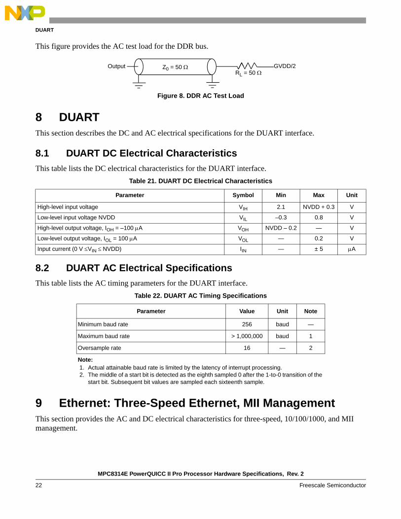
This figure provides the AC test load for the DDR bus.
Figure 8. DDR AC Test Load
8 DUARTThis section describes the DC and AC electrical specifications for the DUART interface.
8.1 DUART DC Electrical CharacteristicsThis table lists the DC electrical characteristics for the DUART interface.
8.2 DUART AC Electrical SpecificationsThis table lists the AC timing parameters for the DUART interface.
9 Ethernet: Three-Speed Ethernet, MII ManagementThis section provides the AC and DC electrical characteristics for three-speed, 10/100/1000, and MII management.
Table 21. DUART DC Electrical Characteristics
Parameter Symbol Min Max Unit
High-level input voltage VIH 2.1 NVDD + 0.3 V
Low-level input voltage NVDD VIL –0.3 0.8 V
High-level output voltage, IOH = –100 A VOH NVDD – 0.2 — V
Low-level output voltage, IOL = 100 A VOL — 0.2 V
Input current (0 V VIN NVDD) IIN — ± 5 A
Table 22. DUART AC Timing Specifications
Parameter Value Unit Note
Minimum baud rate 256 baud —
Maximum baud rate > 1,000,000 baud 1
Oversample rate 16 — 2
Note: 1. Actual attainable baud rate is limited by the latency of interrupt processing.2. The middle of a start bit is detected as the eighth sampled 0 after the 1-to-0 transition of the
start bit. Subsequent bit values are sampled each sixteenth sample.
Output Z0 = 50 GVDD/2RL = 50

MPC8314E PowerQUICC II Pro Processor Hardware Specifications, Rev. 2
Freescale Semiconductor 23
Ethernet: Three-Speed Ethernet, MII Management
9.1 eTSEC (10/100/1000 Mbps)—MII/RMII/RGMII/RTBI Electrical Characteristics
The electrical characteristics specified here apply to all the media-independent interface (MII), reduced gigabit MII (RGMII), and reduced ten-bit interface (RTBI) signals except management data input/output (MDIO) and management data clock (MDC). The MII and RMII is defined for 3.3 V, while the RGMII, and RTBI can operate at 2.5 V. The RGMII and RTBI follow the Hewlett-Packard reduced pin-count interface for Gigabit Ethernet Physical Layer Device Specification Version 1.2a (9/22/2000). The electrical characteristics for MDIO and MDC are specified in Section 9.3, “Ethernet Management Interface Electrical Characteristics.”
9.1.1 MII, RMII, RGMII, and RTBI DC Electrical Characteristics
All MII, RMII drivers and receivers comply with the DC parametric attributes specified in Table 23 for 3.3-V operation and RGMII, RTBI drivers and receivers comply with the DC parametric attributes specified in Table 24. The RGMII and RTBI signals are based on a 2.5 V CMOS interface voltage as defined by JEDEC EIA/JESD8–5.
NOTEeTSEC should be interfaced with peripheral operating at same voltage level.
Table 23. MII/RMII (When Operating at 3.3 V) DC Electrical Characteristics
Parameter Symbol Conditions Min Max Unit
Supply voltage 3.3 V LVDD — — 3.0 3.6 V
Output high voltage VOH IOH = –4.0 mA LVDD = Min 2.40 LVDD + 0.3 V
Output low voltage VOL IOL = 4.0 mA LVDD = Min VSS 0.50 V
Input high voltage VIH — — 2.1 LVDD + 0.3 V
Input low voltage VIL — — –0.3 0.90 V
Input high current IIH VIN 1 = LVDD — 40 A
Input low current IIL VIN 1 = VSS –600 — A
Note: 1. The symbol VIN, in this case, represents the LVIN symbol referenced in Table 1 and Table 2.
Table 24. RGMII/RTBI (When Operating at 2.5 V) DC Electrical Characteristics
Parameters Symbol Conditions Min Max Unit
Supply voltage 2.5 V LVDD — — 2.37 2.63 V
Output high voltage VOH IOH = –1.0 mA LVDD = Min 2.00 LVDD + 0.3 V
Output low voltage VOL IOL = 1.0 mA LVDD = Min VSS– 0.3 0.40 V
Input high voltage VIH — LVDD = Min 1.7 LVDD + 0.3 V
Input low voltage VIL — LVDD =Min –0.3 0.70 V
Input high current IIH VIN 1 = LVDD — 15 A
Input low current IIL VIN 1 = VSS –15 — A

MPC8314E PowerQUICC II Pro Processor Hardware Specifications, Rev. 2
24 Freescale Semiconductor
Ethernet: Three-Speed Ethernet, MII Management
9.2 MII, RMII, RGMII, and RTBI AC Timing SpecificationsThe AC timing specifications for MII, RMII, RGMII, and RTBI are presented in this section.
9.2.1 MII AC Timing SpecificationsThis section describes the MII transmit and receive AC timing specifications.
9.2.1.1 MII Transmit AC Timing Specifications
This table provides the MII transmit AC timing specifications.
This figure shows the MII transmit AC timing diagram.
Figure 9. MII Transmit AC Timing Diagram
Note: 1. The symbol VIN, in this case, represents the LVIN symbol referenced in Table 1 and Table 2.
Table 25. MII Transmit AC Timing SpecificationsAt recommended operating conditions with LVDD of 3.3 V ± 300 mv.
Parameter/Condition Symbol 1 Min Typ Max Unit
TX_CLK clock period 10 Mbps tMTX — 400 — ns
TX_CLK clock period 100 Mbps tMTX — 40 — ns
TX_CLK duty cycle tMTXH/tMTX 35 — 65 %
TX_CLK to MII data TXD[3:0], TX_ER, TX_EN delay tMTKHDX 1 5 15 ns
TX_CLK data clock rise VIL(min) to VIH(max) tMTXR 1.0 — 4.0 ns
TX_CLK data clock fall VIH(max) to VIL(min) tMTXF 1.0 — 4.0 ns
Note: 1. The symbols used for timing specifications follow the pattern of t(first two letters of functional block)(signal)(state)(reference)(state) for
inputs and t(first two letters of functional block)(reference)(state)(signal)(state) for outputs. For example, tMTKHDX symbolizes MII transmit timing (MT) for the time tMTX clock reference (K) going high (H) until data outputs (D) are invalid (X). Note that, in general, the clock reference symbol representation is based on two to three letters representing the clock of a particular functional. For example, the subscript of tMTX represents the MII(M) transmit (TX) clock. For rise and fall times, the latter convention is used with the appropriate letter: R (rise) or F (fall).
Table 24. RGMII/RTBI (When Operating at 2.5 V) DC Electrical Characteristics (continued)
Parameters Symbol Conditions Min Max Unit
TX_CLK
TXD[3:0]
tMTKHDX
tMTX
tMTXH
tMTXR
tMTXF
TX_ENTX_ER

MPC8314E PowerQUICC II Pro Processor Hardware Specifications, Rev. 2
Freescale Semiconductor 25
Ethernet: Three-Speed Ethernet, MII Management
9.2.1.2 MII Receive AC Timing Specifications
This table provides the MII receive AC timing specifications.
This figure provides the AC test load for eTSEC.
Figure 10. eTSEC AC Test Load
This figure shows the MII receive AC timing diagram.
Figure 11. MII Receive AC Timing Diagram RMII AC Timing Specifications
Table 26. MII Receive AC Timing SpecificationsAt recommended operating conditions with LVDD of 3.3 V ± 300 mv
Parameter/Condition Symbol 1 Min Typ Max Unit
RX_CLK clock period 10 Mbps tMRX — 400 — ns
RX_CLK clock period 100 Mbps tMRX — 40 — ns
RX_CLK duty cycle tMRXH/tMRX 35 — 65 %
RXD[3:0], RX_DV, RX_ER setup time to RX_CLK tMRDVKH 10.0 — — ns
RXD[3:0], RX_DV, RX_ER hold time to RX_CLK tMRDXKH 10.0 — — ns
RX_CLK clock rise VIL(min) to VIH(max) tMRXR 1.0 — 4.0 ns
RX_CLK clock fall time VIH(max) to VIL(min) tMRXF 1.0 — 4.0 ns
Note: 1. The symbols used for timing specifications herein follow the pattern of t(first two letters of functional block)(signal)(state)(reference)(state)
for inputs and t(first two letters of functional block)(reference)(state)(signal)(state) for outputs. For example, tMRDVKH symbolizes MII receive timing (MR) with respect to the time data input signals (D) reach the valid state (V) relative to the tMRX clock reference (K) going to the high (H) state or setup time. Also, tMRDXKL symbolizes MII receive timing (GR) with respect to the time data input signals (D) went invalid (X) relative to the tMRX clock reference (K) going to the low (L) state or hold time. Note that, in general, the clock reference symbol representation is based on three letters representing the clock of a particular functional. For example, the subscript of tMRX represents the MII (M) receive (RX) clock. For rise and fall times, the latter convention is used with the appropriate letter: R (rise) or F (fall).
2. The frequency of RX_CLK should not exceed the TX_CLK by more than 300 ppm
Output Z0 = 50 LVDD/2RL = 50
RX_CLK
RXD[3:0]
tMRDXKH
tMRX
tMRXH
tMRXR
tMRXF
RX_DVRX_ER
tMRDVKH
Valid Data

MPC8314E PowerQUICC II Pro Processor Hardware Specifications, Rev. 2
26 Freescale Semiconductor
Ethernet: Three-Speed Ethernet, MII Management
9.2.2 RMII AC Timing SpecificationsThis section describes the RMII transmit and receive AC timing specifications.
9.2.2.1 RMII Transmit AC Timing Specifications
This section describes the RMII transmit and receive AC timing specifications. This table provides the RMII transmit AC timing specifications.
This figure shows the RMII transmit AC timing diagram.
Figure 12. RMII Transmit AC Timing Diagram
9.2.2.2 RMII Receive AC Timing Specifications
This table provides the RMII receive AC timing specifications.
Table 27. RMII Transmit AC Timing SpecificationsAt recommended operating conditions with LVDD of 3.3 V ± 300 mv
Parameter/Condition Symbol 1 Min Typ Max Unit
REF_CLK clock tRMX — 20 — ns
REF_CLK duty cycle tRMXH/tRMX 35 — 65 %
REF_CLK to RMII data TXD[1:0], TX_EN delay tRMTKHDX 2 — 10 ns
REF_CLK data clock rise VIL(min) to VIH(max) tRMXR 1.0 — 4.0 ns
REF_CLK data clock fall VIH(max) to VIL(min) tRMXF 1.0 — 4.0 ns
Note: 1. The symbols used for timing specifications herein follow the pattern of t(first three letters of functional block)(signal)(state) (reference)(state)
for inputs and t(first two letters of functional block)(reference)(state)(signal)(state) for outputs. For example, tRMTKHDX symbolizes RMII transmit timing (RMT) for the time tRMX clock reference (K) going high (H) until data outputs (D) are invalid (X). Note that, in general, the clock reference symbol representation is based on two to three letters representing the clock of a particular functional. For example, the subscript of tRMX represents the RMII(RM) reference (X) clock. For rise and fall times, the latter convention is used with the appropriate letter: R (rise) or F (fall).
Table 28. RMII Receive AC Timing SpecificationsAt recommended operating conditions with LVDD of 3.3 V ± 300 mv
Parameter/Condition Symbol 1 Min Typ Max Unit
REF_CLK clock period tRMX — 20 — ns
REF_CLK duty cycle tRMXH/tRMX 35 — 65 %
REF_CLK
TXD[1:0]
tRMTKHDX
tRMX
tRMXH
tRMXR
tRMXF
TX_EN

MPC8314E PowerQUICC II Pro Processor Hardware Specifications, Rev. 2
Freescale Semiconductor 27
Ethernet: Three-Speed Ethernet, MII Management
This figure provides the AC test load.
Figure 13. AC Test Load
This figure shows the RMII receive AC timing diagram.
Figure 14. RMII Receive AC Timing Diagram
9.2.3 RGMII and RTBI AC Timing Specifications
This table presents the RGMII and RTBI AC timing specifications.
RXD[1:0], CRS_DV, RX_ER setup time to REF_CLK tRMRDVKH 4.0 — — ns
RXD[1:0], CRS_DV, RX_ER hold time to REF_CLK tRMRDXKH 2.0 — — ns
REF_CLK clock rise VIL(min) to VIH(max) tRMXR 1.0 — 4.0 ns
REF_CLK clock fall time VIH(max) to VIL(min) tRMXF 1.0 — 4.0 ns
Note: 1. The symbols used for timing specifications herein follow the pattern of t(first three letters of functional block)(signal)(state) (reference)(state)
for inputs and t(first two letters of functional block)(reference)(state)(signal)(state) for outputs. For example, tRMRDVKH symbolizes RMII receive timing (RMR) with respect to the time data input signals (D) reach the valid state (V) relative to the tRMX clock reference (K) going to the high (H) state or setup time. Also, tRMRDXKL symbolizes RMII receive timing (RMR) with respect to the time data input signals (D) went invalid (X) relative to the tRMX clock reference (K) going to the low (L) state or hold time. Note that, in general, the clock reference symbol representation is based on three letters representing the clock of a particular functional. For example, the subscript of tRMX represents the RMII (RM) reference (X) clock. For rise and fall times, the latter convention is used with the appropriate letter: R (rise) or F (fall).
Table 29. RGMII and RTBI AC Timing SpecificationsAt recommended operating conditions (see Table 2)
Parameter/Condition Symbol 1 Min Typ Max Unit
Data to clock output skew (at transmitter) tSKRGT –0.6 — 0.6 ns
Data to clock input skew (at receiver) 2 tSKRGT 1.0 — 2.6 ns
Table 28. RMII Receive AC Timing Specifications (continued)At recommended operating conditions with LVDD of 3.3 V ± 300 mv
Parameter/Condition Symbol 1 Min Typ Max Unit
Output Z0 = 50 NVDD/2RL = 50
REF_CLK
RXD[1:0]
tRMRDXKH
tRMX
tRMXH
tRMXR
tRMXF
CRS_DVRX_ER
tRMRDVKH
Valid Data

MPC8314E PowerQUICC II Pro Processor Hardware Specifications, Rev. 2
28 Freescale Semiconductor
Ethernet: Three-Speed Ethernet, MII Management
Clock cycle duration 3 tRGT 7.2 8.0 8.8 ns
Duty cycle for 1000Base-T 4, 5 tRGTH/tRGT 45 50 55 %
Duty cycle for 10BASE-T and 100BASE-TX 3, 5 tRGTH/tRGT 40 50 60 %
Rise time (20%–80%) tRGTR — — 0.75 ns
Fall time (20%–80%) tRGTF — — 0.75 ns
GTX_CLK125 reference clock period tG12 6 — 8.0 — ns
GTX_CLK125 reference clock duty cycle tG125H/tG125 47 — 53 %
Note: 1. Note that, in general, the clock reference symbol representation for this section is based on the symbols RGT to represent RGMII
and RTBI timing. For example, the subscript of tRGT represents the RTBI (T) receive (RX) clock. Note also that the notation for rise (R) and fall (F) times follows the clock symbol that is being represented. For symbols representing skews, the subscript is skew (SK) followed by the clock that is being skewed (RGT).
2. This implies that PC board design requires clocks to be routed so that an additional trace delay of greater than 1.5 ns is added to the associated clock signal.
3. For 10 and 100 Mbps, tRGT scales to 400 ns ± 40 ns and 40 ns ± 4 ns, respectively.4. Duty cycle may be stretched/shrunk during speed changes or while transitioning to a received packet's clock domains as long as
the minimum duty cycle is not violated and stretching occurs for no more than three tRGT of the lowest speed transitioned between.5. Duty cycle reference is LVDD/2.6. This symbol is used to represent the external GTX_CLK125 and does not follow the original symbol naming convention. GTX_CLK
supply voltage is fixed at 3.3V inside the chip. If PHY supplies a 2.5 V Clock signal on this input, set TSCOMOBI bit of System I/O configuration register (SICRH) as 1. See the MPC8315E PowerQUICC II Pro Integrated Host Processor Family Reference Manual.
7. The frequency of RX_CLK should not exceed the TX_CLK by more than 300 ppm
Table 29. RGMII and RTBI AC Timing Specifications (continued)At recommended operating conditions (see Table 2)
Parameter/Condition Symbol 1 Min Typ Max Unit

MPC8314E PowerQUICC II Pro Processor Hardware Specifications, Rev. 2
Freescale Semiconductor 29
Ethernet: Three-Speed Ethernet, MII Management
This figure shows the RGMII and RTBI AC timing and multiplexing diagrams.
Figure 15. RGMII and RTBI AC Timing and Multiplexing Diagrams
9.3 Ethernet Management Interface Electrical CharacteristicsThe electrical characteristics specified here apply to MII management interface signals management data input/output (MDIO) and management data clock (MDC). The electrical characteristics for MII, RMII, RGMII, and RTBI are specified in Section 9.1, “eTSEC (10/100/1000 Mbps)—MII/RMII/RGMII/RTBI Electrical Characteristics.”
9.3.1 MII Management DC Electrical Characteristics
The MDC and MDIO are defined to operate at a supply voltage of 3.3 V. The DC electrical characteristics for MDIO and MDC are provided in this table.
Table 30. MII Management DC Electrical Characteristics Powered at 3.3 V
Parameter Symbol Conditions Min Max Unit
Supply voltage (3.3 V) NVDD — — 3.0 3.6 V
Output high voltage VOH IOH = –1.0 mA NVDD = Min 2.10 NVDD + 0.3 V
Output low voltage VOL IOL = 1.0 mA NVDD = Min VSS 0.50 V
Input high voltage VIH — — 2.00 — V
Input low voltage VIL — — — 0.80 V
Input high current IIH NVDD = Max VIN 1 = 2.1 V — 40 A
GTX_CLK
tRGTtRGTH
tSKRGT
TX_CTL
TXD[8:5]TXD[7:4]
TXD[9]TXERR
TXD[4]TXEN
TXD[3:0]
(At Transmitter)
TXD[8:5][3:0]TXD[7:4][3:0]
TX_CLK(At PHY)
RX_CTL
RXD[8:5]RXD[7:4]
RXD[9]RXERR
RXD[4]RXDV
RXD[3:0]RXD[8:5][3:0]RXD[7:4][3:0]
RX_CLK(At Controller)
tSKRGT
tSKRGT
tSKRGT

MPC8314E PowerQUICC II Pro Processor Hardware Specifications, Rev. 2
30 Freescale Semiconductor
Ethernet: Three-Speed Ethernet, MII Management
9.3.2 MII Management AC Electrical Specifications
This table provides the MII management AC timing specifications.
Input low current IIL NVDD = Max VIN = 0.5 V –600 — A
Note: 1. The symbol VIN, in this case, represents the NVIN symbol referenced in Table 1 and Table 2.
Table 31. MII Management AC Timing SpecificationsAt recommended operating conditions with NVDD is 3.3 V ± 300 mv
Parameter/Condition Symbol 1 Min Typ Max Unit Note
MDC frequency fMDC — 2.5 — MHz 2
MDC period tMDC — 400 — ns —
MDC clock pulse width high tMDCH 32 — — ns —
MDC to MDIO delay tMDKHDX 10 — 170 ns 3
MDIO to MDC setup time tMDDVKH 5 — — ns —
MDIO to MDC hold time tMDDXKH 0 — — ns —
MDC rise time tMDCR — — 10 ns —
MDC fall time tMDHF — — 10 ns —
Note: 1. The symbols used for timing specifications herein follow the pattern of t(first two letters of functional block)(signal)(state)(reference)(state)
for inputs and t(first two letters of functional block)(reference)(state)(signal)(state) for outputs. For example, tMDKHDX symbolizes management data timing (MD) for the time tMDC from clock reference (K) high (H) until data outputs (D) are invalid (X) or data hold time. Also, tMDDVKH symbolizes management data timing (MD) with respect to the time data input signals (D) reach the valid state (V) relative to the tMDC clock reference (K) going to the high (H) state or setup time. For rise and fall times, the latter convention is used with the appropriate letter: R (rise) or F (fall).
2. This parameter is dependent on the csb_clk speed (that is, for a csb_clk of 133 MHz, the maximum frequency is 4.16 MHz and the minimum frequency is 0.593 MHz).
3. This parameter is dependent on the csb_clk speed (that is, for a csb_clk of 133 MHz, the delay is 60 ns).
Table 30. MII Management DC Electrical Characteristics Powered at 3.3 V (continued)
Parameter Symbol Conditions Min Max Unit

MPC8314E PowerQUICC II Pro Processor Hardware Specifications, Rev. 2
Freescale Semiconductor 31
Ethernet: Three-Speed Ethernet, MII Management
This figure shows the MII management AC timing diagram.
Figure 16. MII Management Interface Timing Diagram
9.4 1588 Timer SpecificationsThis section describes the DC and AC electrical specifications for the 1588 timer.
9.4.1 1588 Timer DC SpecificationsThis table provides the 1588 timer DC specifications.
9.4.2 1588 Timer AC Specifications
This table provides the 1588 timer AC specifications.
Table 32. GPIO DC Electrical Characteristics
Characteristic Symbol Condition Min Max Unit
Output high voltage VOH IOH = –8.0 mA 2.4 — V
Output low voltage VOL IOL = 8.0 mA — 0.5 V
Output low voltage VOL IOL = 3.2 mA — 0.4 V
Input high voltage VIH — 2.0 NVDD + 0.3 V
Input low voltage VIL — –0.3 0.8 V
Input current IIN 0 V VIN NVDD — ± 5 A
Table 33. 1588 Timer AC Specifications
Parameter Symbol Min Max Unit Note
Timer clock cycle time tTMRCK 0 70 MHz 1
Input setup to timer clock tTMRCKS — — — 2, 3
Input hold from timer clock tTMRCKH — — — 2, 3
Output clock to output valid tGCLKNV 0 6 ns
Timer alarm to output valid tTMRAL — — — 2
MDC
tMDDXKH
tMDC
tMDCH
tMDCR
tMDCF
tMDDVKH
tMDKHDX
MDIO
MDIO
(Input)
(Output)

MPC8314E PowerQUICC II Pro Processor Hardware Specifications, Rev. 2
32 Freescale Semiconductor
Ethernet: Three-Speed Ethernet, MII Management
9.5 SGMII Interface Electrical CharacteristicsEach SGMII port features a 4-wire AC-Coupled serial link from the dedicated SerDes interface of MPC8315E as shown in Figure 17, where CTX is the external (on board) AC-Coupled capacitor. Each output pin of the SerDes transmitter differential pair features 50-output impedance. Each input of the SerDes receiver differential pair features 50- on-die termination to XCOREVSS. The reference circuit of the SerDes transmitter and receiver is shown in Figure 48.
When an eTSEC port is configured to operate in SGMII mode, the parallel interface’s output signals of this eTSEC port can be left floating. The input signals should be terminated based on the guidelines described in Section 25.4, “Connection Recommendations,” as long as such termination does not violate the desired POR configuration requirement on these pins, if applicable.
When operating in SGMII mode, the TSEC_GTX_CLK125 clock is not required for this port. Instead, SerDes reference clock is required on SD_REF_CLK and SD_REF_CLK pins.
9.5.1 DC Requirements for SGMII SD_REF_CLK and SD_REF_CLKThe characteristics and DC requirements of the separate SerDes reference clock are described in Section 15, “High-Speed Serial Interfaces (HSSI).”
9.5.2 AC Requirements for SGMII SD_REF_CLK and SD_REF_CLK
This table lists the SGMII SerDes reference clock AC requirements. Please note that SD_REF_CLK and SD_REF_CLK are not intended to be used with, and should not be clocked by, a spread spectrum clock source.
9.5.3 SGMII Transmitter and Receiver DC Electrical Characteristics
Table 35 and Table 36 describe the SGMII SerDes transmitter and receiver AC-coupled DC electrical characteristics. Transmitter DC characteristics are measured at the transmitter outputs (SD_TX[n] and SD_TX[n]) as depicted in Figure 16.
Note: 1. The timer can operate on rtc_clock or tmr_clock. These clocks get muxed and any one of them can be selected.2. Asynchronous signals.3. Inputs need to be stable at least one TMR clock.
Table 34. SD_REF_CLK and SD_REF_CLK AC Requirements
Symbol Parameter Description Min Typical Max Unit Note
tREF REFCLK cycle time — 8 — ns —
tREFCJ REFCLK cycle-to-cycle jitter. Difference in the period of any two adjacent REFCLK cycles
— — 100 ps —
tREFPJ Phase jitter. Deviation in edge location with respect to mean edge location –50 — 50 ps —
Table 33. 1588 Timer AC Specifications (continued)
Parameter Symbol Min Max Unit Note

MPC8314E PowerQUICC II Pro Processor Hardware Specifications, Rev. 2
Freescale Semiconductor 33
Ethernet: Three-Speed Ethernet, MII Management
Table 35. SGMII DC Transmitter Electrical Characteristics
Parameter Symbol Min Typ Max Unit Note
Supply Voltage XCOREVDD 0.95 1.0 1.05 V —
Output high voltage VOH — — XCOREVDD-Typ/2 + |VOD|-max/2
mV 1
Output low voltage VOL XCOREVDD-Typ/2 - |VOD|-max/2
— — mV 1
Output ringing VRING — — 10 % —
Output differential voltage2, 3, 5
|VOD|
323 500 725
mV
Equalization setting: 1.0x
296 459 665 Equalization setting: 1.09x
269 417 604 Equalization setting: 1.2x
243 376 545 Equalization setting: 1.33x
215 333 483 Equalization setting: 1.5x
189 292 424 Equalization setting: 1.71x
162 250 362 Equalization setting: 2.0x
Output offset voltage VOS 425 500 575 mV 1, 4
Output impedance (single-ended) RO 40 — 60 —
Mismatch in a pair RO — — 10 % —
Change in VOD between “0” and “1” |VOD| — — 25 mV —
Change in VOS between “0” and “1” VOS — — 25 mV —
Output current on short to GND ISA, ISB — — 40 mA —
Note: 1. This will not align to DC-coupled SGMII. XCOREVDD-Typ=1.0V.2. |VOD| = |VTXn - VTXn|. |VOD| is also referred as output differential peak voltage. VTX-DIFFp-p = 2*|VOD|.3. The |VOD| value shown in the table assumes the following transmit equalization setting in the TXEQA (for SerDes lane A) or
TXEQE (for SerDes lane E) bit field of MPC8315E’s SerDes Control Register 0: • The LSbits (bit [1:3]) of the above bit field is set based on the equalization setting shown in table.
4. VOS is also referred to as output common mode voltage.5. The |VOD| value shown in the Typ column is based on the condition of XCOREVDD-Typ=1.0V, no common mode offset variation
(VOS = 500 mV), SerDes transmitter is terminated with 100- differential load between TX[n] and TX[n].

MPC8314E PowerQUICC II Pro Processor Hardware Specifications, Rev. 2
34 Freescale Semiconductor
Ethernet: Three-Speed Ethernet, MII Management
Figure 17. 4-Wire AC-Coupled SGMII Serial Link Connection Example
Figure 18. SGMII Transmitter DC Measurement Circuit
Table 36. SGMII DC Receiver Electrical Characteristics
Parameter Symbol Min Typ Max Unit Note
Supply Voltage XCOREVDD 0.95 1.0 1.05 V —
DC Input voltage range — N/A — 1
Input differential voltage EQ = 0 VRX_DIFFp-p 100 — 1200 mV 2, 4
EQ = 1 175 —
Loss of signal threshold EQ = 0 VLOS 30 — 100 mV 3, 4
EQ = 1 65 — 175
MPC8315E SGMIISerDes Interface
50
50 Transmitter
TXn RXm
TXn RXm
Receiver
CTX
CTX
50
50
RXn
RXn
Receiver Transmitter
TXm
TXm
CTX
CTX
50
50
50
50
50
Transmitter
TXn
TXn50
Vos VOD
MPC8315E SGMIISerDes Interface
50
50

MPC8314E PowerQUICC II Pro Processor Hardware Specifications, Rev. 2
Freescale Semiconductor 35
Ethernet: Three-Speed Ethernet, MII Management
9.5.4 SGMII AC Timing SpecificationsThis section describes the SGMII transmit and receive AC timing specifications. Transmitter and receiver characteristics are measured at the transmitter outputs (TX[n] and TX[n]) or at the receiver inputs (RX[n] and RX[n]) as depicted in Figure 20 respectively.
9.5.4.1 SGMII Transmit AC Timing Specifications
This table provides the SGMII transmit AC timing targets. A source synchronous clock is not provided.
9.5.4.2 SGMII Receive AC Timing Specifications
This table provides the SGMII receive AC timing specifications. Source synchronous clocking is not supported. Clock is recovered from the data. Figure 19 shows the SGMII Receiver Input Compliance Mask eye diagram.
Input AC common mode voltage VCM_ACp-p — — 100 mV 5
Receiver differential input impedance ZRX_DIFF 80 100 120 —
Receiver common mode input impedance
ZRX_CM 20 — 35 —
Common mode input voltage VCM — Vxcorevss — V 6
Note: 1. Input must be externally AC-coupled.2. VRX_DIFFp-p is also referred to as peak to peak input differential voltage3. The concept of this parameter is equivalent to the Electrical Idle Detect Threshold parameter in PCI Express. Refer to PCI
Express Differential Receiver (RX) Input Specifications section for further explanation.4. The EQ shown in the table refers to the RXEQA or RXEQE bit field of MPC8315E’s SerDes Control Register 0.5. VCM_ACp-p is also referred to as peak to peak AC common mode voltage.6. On-chip termination to XCOREVSS.
Table 37. SGMII Transmit AC Timing SpecificationsAt recommended operating conditions with XCOREVDD = 1.0V ± 5%.
Parameter Symbol Min Typ Max Unit Note
Deterministic Jitter JD — — 0.17 UI p-p —
Total Jitter JT — — 0.35 UI p-p —
Unit Interval UI 799.92 800 800.08 ps —
VOD fall time (80%-20%) tfall 50 — 120 ps —
VOD rise time (20%-80%) trise 50 — 120 ps —
Note: 1. Each UI is 800 ps ± 100 ppm.
Table 36. SGMII DC Receiver Electrical Characteristics (continued)
Parameter Symbol Min Typ Max Unit Note

MPC8314E PowerQUICC II Pro Processor Hardware Specifications, Rev. 2
36 Freescale Semiconductor
Ethernet: Three-Speed Ethernet, MII Management
Figure 19. SGMII Receiver Input Compliance Mask
Table 38. SGMII Receive AC Timing SpecificationsAt recommended operating conditions with XCOREVDD = 1.0V ± 5%.
Parameter Symbol Min Typ Max Unit Note
Deterministic Jitter Tolerance JD 0.37 — — UI p-p 1
Combined Deterministic and Random Jitter Tolerance JDR 0.55 — — UI p-p 1
Sinusoidal Jitter Tolerance JSIN 0.1 — — UI p-p 1
Total Jitter Tolerance JT 0.65 — — UI p-p 1
Bit Error Ratio BER — — 10-12 —
Unit Interval UI 799.92 800 800.08 ps 2
AC Coupling Capacitor CTX 5 — 200 nF 3
Note: 1. Measured at receiver.2. Each UI is 800 ps ± 100 ppm.3. The external AC coupling capacitor is required. It’s recommended to be placed near the device transmitter outputs.4. Refer to RapidIOTM 1x/4x LP Serial Physical Layer Specification for interpretation of jitter specifications.
Time (UI)
Rec
eive
r D
iffer
entia
l Inp
ut V
olta
ge
0
0.275 0.4 0.6 0.725
VRX_DIFFp-p-min/2
VRX_DIFFp-p-min/2
VRX_DIFFp-p-max/2
VRX_DIFFp-p-max/2
0 1

MPC8314E PowerQUICC II Pro Processor Hardware Specifications, Rev. 2
Freescale Semiconductor 37
USB
Figure 20. SGMII AC Test/Measurement Load
10 USB
10.1 USB Dual-Role ControllersThis section provides the AC and DC electrical specifications for the USB-ULPI interface.
10.1.1 USB DC Electrical Characteristics
This table lists the DC electrical characteristics for the USB interface.
10.1.2 USB AC Electrical Specifications
This table lists the general timing parameters of the USB-ULPI interface.
Table 39. USB DC Electrical Characteristics
Parameter Symbol Min Max Unit
High-level input voltage VIH 2 LVDD + 0.3 V
Low-level input voltage VIL –0.3 0.8 V
Input current IIN — ±5 A
High-level output voltage, IOH = –100 A VOH LVDD – 0.2 — V
Low-level output voltage, IOL = 100 A VOL — 0.2 V
Note: 1. The symbol VIN, in this case, represents the NVIN symbol referenced in Table 1 and Table 2.
Table 40. USB General Timing Parameters
Parameter Symbol 1 Min Max Unit Note
USB clock cycle time tUSCK 15 — ns 1, 2
Input setup to USB clock—all inputs tUSIVKH 4 — ns 1, 4
Input hold to USB clock—all inputs tUSIXKH 1 — ns 1, 4

MPC8314E PowerQUICC II Pro Processor Hardware Specifications, Rev. 2
38 Freescale Semiconductor
USB
Figure 21 and Figure 22 provide the AC test load and signals for the USB, respectively.
Figure 21. USB AC Test Load
Figure 22. USB Signals
10.2 On-Chip USB PHYThis section provides the AC and DC electrical specifications for the USB PHY interface of the MPC8314E.
For details refer to Tables 7-7 through 7-10, and Table 7-14 in the USB 2.0 Specifications document, and the pull-up/down resistors ECN updates, all available at www.usb.org.
This table provides the USB clock input (USB_CLK_IN) DC timing specifications.
USB clock to output valid—all outputs tUSKHOV — 9 ns 1
Output hold from USB clock—all outputs tUSKHOX 1 — ns 1
Note: 1. The symbols used for timing specifications follow the pattern of t(First two letters of functional block)(signal)(state)(reference)(state) for
inputs and t(First two letters of functional block)(reference)(state)(signal)(state) for outputs. For example, tUSIXKH symbolizes USB timing (US) for the input (I) to go invalid (X) with respect to the time the USB clock reference (K) goes high (H). Also, tUSKHOX symbolizes USB timing (US) for the us clock reference (K) to go high (H), with respect to the output (O) going invalid (X) or output hold time.
2. All timings are in reference to USB clock.3. All signals are measured from NVDD/2 of the rising edge of USB clock to 0.4 NVDD of the signal in question for 3.3-V
signaling levels.4. Input timings are measured at the pin.5. For purposes of active/float timing measurements, the Hi-Z or off-state is defined to be when the total current delivered through
the component pin is less than or equal to the leakage current specification.
Table 40. USB General Timing Parameters (continued)
Parameter Symbol 1 Min Max Unit Note
Output Z0 = 50 NVDD/2RL = 50
Output Signals
tUSKHOV
USBDR_CLK
Input Signals
tUSIXKHtUSIVKH
tUSKHOX

MPC8314E PowerQUICC II Pro Processor Hardware Specifications, Rev. 2
Freescale Semiconductor 39
Local Bus
This table provides the USB clock input (USB_CLK_IN) AC timing specifications.
11 Local BusThis section describes the DC and AC electrical specifications for the local bus interface of the MPC8314E.
11.1 Local Bus DC Electrical CharacteristicsThis table provides the DC electrical characteristics for the local bus interface.
11.2 Local Bus AC Electrical SpecificationsThis table describes the general timing parameters of the local bus interface of the MPC8314E.
Table 41. USB_CLK_IN DC Electrical Characteristics
Parameter Symbol Min Max Unit
Input high voltage VIH 2.7 NVDD + 0.3 V
Input low voltage VIL –0.3 0.4 V
Table 42. USB_CLK_IN AC Timing Specifications
Parameter/Condition Conditions Symbol Min Typical Max Unit
Frequency range — fUSB_CLK_IN — 24 — MHz
Clock frequency tolerance — tCLK_TOL –0.005 0 0.005 %
Reference clock duty cycle Measured at 1.6 V tCLK_DUTY 40 50 60 %
Total input jitter/Time interval error
Peak to peak value measured with a second order high-pass filter of 500 KHz bandwidth
tCLK_PJ — — 200 ps
Table 43. DC Electrical Characteristics (when Operating at 3.3 V)
Parameter Symbol Min Max Unit
Output high voltage (NVDD = min, IOH = –2 mA) VOH NVDD – 0.2 — V
Output low voltage (NVDD = min, IOL = 2 mA) VOL — 0.2 V
Input high voltage VIH 2 NVDD + 0.3 V
Input low voltage VIL –0.3 0.8 V
Input high current (VIN = 0 V or VIN = NVDD) IIN — ±5 A
Table 44. Local Bus General Timing Parameters
Parameter Symbol 1 Min Max Unit Note
Local bus cycle time tLBK 15 — ns 2
Input setup to local bus clock tLBIVKH 7 — ns 3, 4

MPC8314E PowerQUICC II Pro Processor Hardware Specifications, Rev. 2
40 Freescale Semiconductor
Local Bus
This figure provides the AC test load for the local bus.
Figure 23. Local Bus AC Test Load
Input hold from local bus clock tLBIXKH 1.0 — ns 3, 4
LALE output fall to LAD output transition (LATCH hold time) tLBOTOT1 1.5 — ns 5
LALE output fall to LAD output transition (LATCH hold time) tLBOTOT2 3 — ns 6
LALE output fall to LAD output transition (LATCH hold time) tLBOTOT3 2.5 — ns 7
Local bus clock to output valid tLBKHOV — 3 ns 3
Local bus clock to output high impedance for LAD tLBKHOZ — 4 ns 8
LALE output rise to LCLK negative edge tLALEHOV — 3.0 ns
Note: 1. The symbols used for timing specifications herein follow the pattern of t(First two letters of functional
block)(signal)(state)(reference)(state) for inputs and t(First two letters of functional block)(reference)(state)(signal)(state) for outputs. For example, tLBIXKH1 symbolizes local bus timing (LB) for the input (I) to go invalid (X) with respect to the time the tLBK clock reference (K) goes high (H), in this case for clock one(1). Also, tLBKHOX symbolizes local bus timing (LB) for the tLBK clock reference (K) to go high (H), with respect to the output (O) going invalid (X) or output hold time.
2. All timings are in reference to falling edge of LCLK0 (for all outputs and for LGTA and LUPWAIT inputs) or rising edge of LCLK0 (for all other inputs).
3. All signals are measured from NVDD/2 of the rising/falling edge of LCLK0 to 0.4 NVDD of the signal in question for 3.3-V signaling levels.
4. Input timings are measured at the pin.5. tLBOTOT1 should be used when RCWH[LALE] is not set and the load on LALE output pin is at least 10pF less than the load
on LAD output pins.6. tLBOTOT2 should be used when RCWH[LALE] is set and the load on LALE output pin is at least 10pF less than the load on
LAD output pins.7. tLBOTOT3 should be used when RCWH[LALE] is set and the load on LALE output pin equals to the load on LAD output pins. 8. For active/float timing measurements, the Hi-Z or off state is defined to be when the total current delivered through the
component pin is less than or equal to the leakage current specification.
Table 44. Local Bus General Timing Parameters (continued)
Parameter Symbol 1 Min Max Unit Note
Output Z0 = 50 NVDD/2RL = 50

MPC8314E PowerQUICC II Pro Processor Hardware Specifications, Rev. 2
Freescale Semiconductor 41
Local Bus
Figure 24 through Figure 26 show the local bus signals.
Figure 24. Local Bus Signals, Nonspecial Signals Only
Figure 25. Local Bus Signals, GPCM/UPM Signals for LCRR[CLKDIV] = 2
Output Signals:
LBCTL/LBCKE/LOE/
tLBKHOV
tLBKHOV
LCLK[n]
Input Signals:LAD[0:15]
Output Signals:LAD[0:15]
tLBIXKHtLBIVKH
tLBKHOZ
tLBOTOT
LALE
Input Signal:LGTA
tLBIXKHtLBIVKH
tLBIXKH
tLALEHOV
LCLK
UPM Mode Input Signal:LUPWAIT
tLBIXKHtLBIVKH
tLBIVKH
tLBIXKH
tLBKHOZ
T1
T3
Input Signals:LAD[0:15]
UPM Mode Output Signals:LCS[0:3]/LBS[0:1]/LGPL[0:5]
GPCM Mode Output Signals:LCS[0:3]/LWE
tLBKHOV
tLBKHOV
tLBKHOZ

MPC8314E PowerQUICC II Pro Processor Hardware Specifications, Rev. 2
42 Freescale Semiconductor
JTAG
Figure 26. Local Bus Signals, GPCM/UPM Signals for LCRR[CLKDIV] = 4
12 JTAGThis section describes the DC and AC electrical specifications for the IEEE Std 1149.1™ (JTAG) interface.
12.1 JTAG DC Electrical CharacteristicsThis table provides the DC electrical characteristics for the IEEE 1149.1 (JTAG) interface.
Table 45. JTAG Interface DC Electrical Characteristics
Characteristic Symbol Condition Min Max Unit
Input high voltage VIH — 2.1 NVDD + 0.3 V
Input low voltage VIL — –0.3 0.8 V
Input current IIN — — ±5 A
Output high voltage VOH IOH = –8.0 mA 2.4 — V
Output low voltage VOL IOL = 8.0 mA — 0.5 V
Output low voltage VOL IOL = 3.2 mA — 0.4 V
LCLK
UPM Mode Input Signal:LUPWAIT
tLBIXKHtLBIVKH
tLBIVKH
tLBIXKH
tLBKHOZ
T1
T3
UPM Mode Output Signals:LCS[0:3]/LBS[0:1]/LGPL[0:5]
GPCM Mode Output Signals:LCS[0:3]/LWE
tLBKHOV
tLBKHOV
tLBKHOZ
T2
T4
Input Signals:LAD[0:15]

MPC8314E PowerQUICC II Pro Processor Hardware Specifications, Rev. 2
Freescale Semiconductor 43
JTAG
12.2 JTAG AC Timing SpecificationsThis section describes the AC electrical specifications for the IEEE 1149.1 (JTAG) interface. This table provides the JTAG AC timing specifications as defined in Figure 28 through Figure 31.
Table 46. JTAG AC Timing Specifications (Independent of SYS_CLK_IN) 1
At recommended operating conditions (see Table 2)
Parameter Symbol 2 Min Max Unit Note
JTAG external clock frequency of operation fJTG 0 33.3 MHz —
JTAG external clock cycle time t JTG 30 — ns —
JTAG external clock pulse width measured at 1.4 V tJTKHKL 15 — ns —
JTAG external clock rise and fall times tJTGR, tJTGF 0 2 ns —
TRST assert time tTRST 25 — ns 3
Input setup times:Boundary-scan data
TMS, TDItJTDVKHtJTIVKH
44
——
ns 4
Input hold times:Boundary-scan data
TMS, TDItJTDXKHtJTIXKH
1010
——
ns 4
Valid times:Boundary-scan data
TDOtJTKLDVtJTKLOV
22
1111
ns 5
Output hold times:Boundary-scan data
TDOtJTKLDXtJTKLOX
22
——
ns 5
JTAG external clock to output high impedance:Boundary-scan data
TDOtJTKLDZtJTKLOZ
22
199
ns 5, 6
Note: 1. All outputs are measured from the midpoint voltage of the falling/rising edge of tTCLK to the midpoint of the signal in question.
The output timings are measured at the pins. All output timings assume a purely resistive 50-load (see Table 27). Time-of-flight delays must be added for trace lengths, vias, and connectors in the system.
2. The symbols used for timing specifications herein follow the pattern of t(first two letters of functional block)(signal)(state) (reference)(state) for inputs and t(first two letters of functional block)(reference)(state)(signal)(state) for outputs. For example, tJTDVKH symbolizes JTAG device timing (JT) with respect to the time data input signals (D) reaching the valid state (V) relative to the tJTG clock reference (K) going to the high (H) state or setup time. Also, tJTDXKH symbolizes JTAG timing (JT) with respect to the time data input signals (D) went invalid (X) relative to the tJTG clock reference (K) going to the high (H) state. Note that, in general, the clock reference symbol representation is based on three letters representing the clock of a particular functional. For rise and fall times, the latter convention is used with the appropriate letter: R (rise) or F (fall).
3. TRST is an asynchronous level sensitive signal. The setup time is for test purposes only.4. Non-JTAG signal input timing with respect to tTCLK.5. Non-JTAG signal output timing with respect to tTCLK.6. Guaranteed by design and characterization.

MPC8314E PowerQUICC II Pro Processor Hardware Specifications, Rev. 2
44 Freescale Semiconductor
JTAG
This figure provides the AC test load for TDO and the boundary-scan outputs of the MPC8314E.
Figure 27. AC Test Load for the JTAG Interface
This figure provides the JTAG clock input timing diagram.
Figure 28. JTAG Clock Input Timing Diagram
This figure provides the TRST timing diagram.
Figure 29. TRST Timing Diagram
This figure provides the boundary-scan timing diagram.
Figure 30. Boundary-Scan Timing Diagram
Output Z0 = 50 NVDD/2RL = 50
JTAG
tJTKHKL tJTGR
External Clock VMVMVM
tJTG tJTGF
VM = Midpoint Voltage (NVDD/2)
TRST
VM = Midpoint Voltage (NVDD/2)
VM VM
tTRST
VM = Midpoint Voltage (NVDD/2)
VM VM
tJTDVKHtJTDXKH
BoundaryData Outputs
BoundaryData Outputs
JTAGExternal Clock
BoundaryData Inputs
Output Data Valid
tJTKLDX
tJTKLDZ
tJTKLDV
InputData Valid
Output Data Valid

MPC8314E PowerQUICC II Pro Processor Hardware Specifications, Rev. 2
Freescale Semiconductor 45
I2C
This figure provides the test access port timing diagram.
Figure 31. Test Access Port Timing Diagram
13 I2C This section describes the DC and AC electrical characteristics for the I2C interface of the MPC8314E.
13.1 I2C DC Electrical CharacteristicsThis table provides the DC electrical characteristics for the I2C interface.
Table 47. I2C DC Electrical CharacteristicsAt recommended operating conditions with NVDD of 3.3 V ± 300 mv
Parameter Symbol Min Max Unit Note
Input high voltage level VIH 0.7 NVDD NVDD + 0.3 V —
Input low voltage level VIL –0.3 0.3 NVDD V —
Low level output voltage VOL 0 0.2 NVDD V 1
High level output voltage VOH 0.8 NVDD NVDD + 0.3 V —
Output fall time from VIH(min) to VIL(max) with a bus capacitance from 10 to 400 pF
tI2KLKV 20 + 0.1 CB 250 ns 2
Pulse width of spikes which must be suppressed by the input filter
tI2KHKL 0 50 ns 3
Capacitance for each I/O pin CI — 10 pF —
Input current (0 V VIN NVDD) IIN — ± 5 A 4
Note: 1. Output voltage (open drain or open collector) condition = 3 mA sink current.2. CB = capacitance of one bus line in pF.3. See the MPC8315E PowerQUICC II Pro Integrated Host Processor Family Reference Manual for information on the digital
filter used.4. I/O pins obstruct the SDA and SCL lines if NVDD is switched off.
VM = Midpoint Voltage (NVDD/2)
VM VM
tJTIVKHtJTIXKH
JTAGExternal Clock
Output Data Valid
tJTKLOX
tJTKLOZ
tJTKLOV
InputData Valid
Output Data Valid
TDI, TMS
TDO
TDO

MPC8314E PowerQUICC II Pro Processor Hardware Specifications, Rev. 2
46 Freescale Semiconductor
I2C
13.2 I2C AC Electrical SpecificationsThis table provides the AC timing parameters for the I2C interface.
This figure provides the AC test load for the I2C.
Figure 32. I2C AC Test Load
Table 48. I2C AC Electrical SpecificationsAll values refer to VIH (min) and VIL (max) levels (see Table 47)
Parameter Symbol 1 Min Max Unit
SCL clock frequency fI2C 0 400 kHz
Low period of the SCL clock tI2CL 1.3 — s
High period of the SCL clock tI2CH 0.6 — s
Setup time for a repeated START condition tI2SVKH 0.6 — s
Hold time (repeated) START condition (after this period, the first clock pulse is generated)
tI2SXKL 0.6 — s
Data setup time tI2DVKH 100 — ns
Data hold time:CBUS compatible masters
I2C bus devices
tI2DXKL—0 2
—0.9 3
s
Fall time of both SDA and SCL signals tI2CF 4 — 300 ns
Setup time for STOP condition tI2PVKH 0.6 — s
Bus free time between a STOP and START condition tI2KHDX 1.3 — s
Noise margin at the LOW level for each connected device (including hysteresis) VNL 0.1 NVDD — V
Noise margin at the HIGH level for each connected device (including hysteresis) VNH 0.2 NVDD — V
Note: 1. The symbols used for timing specifications follow the pattern of t(first two letters of functional block)(signal)(state)(reference)(state) for
inputs and t(first two letters of functional block)(reference)(state)(signal)(state) for outputs. For example, tI2DVKH symbolizes I2C timing (I2) with respect to the time data input signals (D) reach the valid state (V) relative to the tI2C clock reference (K) going to the high (H) state or setup time. Also, tI2SXKL symbolizes I2C timing (I2) for the time that the data with respect to the start condition (S) went invalid (X) relative to the tI2C clock reference (K) going to the low (L) state or hold time. Also, tI2PVKH symbolizes I2C timing (I2) for the time that the data with respect to the stop condition (P) reaching the valid state (V) relative to the tI2C clock reference (K) going to the high (H) state or setup time. For rise and fall times, the latter convention is used with the appropriate letter: R (rise) or F (fall).
2. MPC8314E provides a hold time of at least 300 ns for the SDA signal (referred to the VIHmin of the SCL signal) to bridge the undefined region of the falling edge of SCL.
3. The maximum tI2DVKH has to be met only if the device does not stretch the LOW period (tI2CL) of the SCL signal.4. MPC8314E does not follow the I2C-BUS Specifications version 2.1 regarding the tI2CF AC parameter.
Output Z0 = 50 NVDD/2RL = 50

MPC8314E PowerQUICC II Pro Processor Hardware Specifications, Rev. 2
Freescale Semiconductor 47
PCI
This figure shows the AC timing diagram for the I2C bus.
Figure 33. I2C Bus AC Timing Diagram
14 PCIThis section describes the DC and AC electrical specifications for the PCI bus of the MPC8314E.
14.1 PCI DC Electrical CharacteristicsThis table provides the DC electrical characteristics for the PCI interface.
14.2 PCI AC Electrical SpecificationsThis section describes the general AC timing parameters of the PCI bus. Note that the PCI_CLK or PCI_SYNC_IN signal is used as the PCI input clock depending on whether the MPC8314E is configured as a host or agent device. This table shows the PCI AC timing specifications at 66 MHz.
.
Table 49. PCI DC Electrical Characteristics 1
Parameter Symbol Test Condition Min Max Unit
High-level input voltage VIH VOUT VOH (min) or 0.5 x NVDD NVDD + 0.3 V
Low-level input voltage VIL VOUT VOL (max) –0.5 0.3 NVDD V
High-level output voltage VOH NVDD = min,IOH = –500 A
0.9 x NVDD — V
Low-level output voltage VOL NVDD = min, IOL = 1500 A
— 0.1 x NVDD V
Input current IIN 0 V VIN NVDD — ± 10 A
Note: 1. The symbol VIN, in this case, represents the NVIN symbol referenced in Table 1 and Table 2.
Table 50. PCI AC Timing Specifications at 66 MHz
Parameter Symbol 1 Min Max Unit Note
Clock to output valid tPCKHOV — 6.0 ns 2
Output hold from clock tPCKHOX 1 — ns 2
Clock to output high impedance tPCKHOZ — 14 ns 2, 3
Input setup to clock tPCIVKH 3.3 — ns 2, 4
SrS
SDA
SCL
tI2CF
tI2SXKL
tI2CL
tI2CHtI2DXKL
tI2DVKH
tI2SXKL
tI2SVKH
tI2KHKL
tI2PVKH
tI2CR
tI2CF
P S

MPC8314E PowerQUICC II Pro Processor Hardware Specifications, Rev. 2
48 Freescale Semiconductor
PCI
This table shows the PCI AC Timing Specifications at 33 MHz.
This figure provides the AC test load for PCI.
Figure 34. PCI AC Test Load
Input hold from clock tPCIXKH 0 — ns 2, 4
Note: 1. Note that the symbols used for timing specifications herein follow the pattern of t(first two letters of functional block)(signal)(state)
(reference)(state) for inputs and t(first two letters of functional block)(reference)(state)(signal)(state) for outputs. For example, tPCIVKH symbolizes PCI timing (PC) with respect to the time the input signals (I) reach the valid state (V) relative to the PCI_SYNC_IN clock, tSYS, reference (K) going to the high (H) state or setup time. Also, tPCRHFV symbolizes PCI timing (PC) with respect to the time hard reset (R) went high (H) relative to the frame signal (F) going to the valid (V) state.
2. See the timing measurement conditions in the PCI 2.3 Local Bus Specifications. 3. For purposes of active/float timing measurements, the Hi-Z or off state is defined to be when the total current delivered
through the component pin is less than or equal to the leakage current specification.4. Input timings are measured at the pin.
Table 51. PCI AC Timing Specifications at 33 MHz
Parameter Symbol 1 Min Max Unit Note
Clock to output valid tPCKHOV — 11 ns 2
Output hold from clock tPCKHOX 2 — ns 2
Clock to output high impedance tPCKHOZ — 14 ns 2, 3
Input setup to clock tPCIVKH 4.0 — ns 2, 4
Input hold from clock tPCIXKH 0 — ns 2, 4
Note: 1. Note that the symbols used for timing specifications follow the pattern of t(first two letters of functional block)(signal)(state)
(reference)(state) for inputs and t(first two letters of functional block)(reference)(state)(signal)(state) for outputs. For example, tPCIVKH symbolizes PCI timing (PC) with respect to the time the input signals (I) reach the valid state (V) relative to the PCI_SYNC_IN clock, tSYS, reference (K) going to the high (H) state or setup time. Also, tPCRHFV symbolizes PCI timing (PC) with respect to the time hard reset (R) went high (H) relative to the frame signal (F) going to the valid (V) state.
2. See the timing measurement conditions in the PCI 2.3 Local Bus Specifications.3. For purposes of active/float timing measurements, the Hi-Z or off state is defined to be when the total current delivered
through the component pin is less than or equal to the leakage current specification.4. Input timings are measured at the pin.
Table 50. PCI AC Timing Specifications at 66 MHz (continued)
Parameter Symbol 1 Min Max Unit Note
Output Z0 = 50 NVDD/2RL = 50

MPC8314E PowerQUICC II Pro Processor Hardware Specifications, Rev. 2
Freescale Semiconductor 49
High-Speed Serial Interfaces (HSSI)
This figure shows the PCI input AC timing conditions.
Figure 35. PCI Input AC Timing Measurement Conditions
This figure shows the PCI output AC timing conditions.
Figure 36. PCI Output AC Timing Measurement Condition
15 High-Speed Serial Interfaces (HSSI)This section describes the common portion of SerDes DC electrical specifications, which is the DC requirement for SerDes Reference Clocks. The SerDes data lane’s transmitter and receiver reference circuits are also shown.
15.1 Signal Terms DefinitionThe SerDes utilizes differential signaling to transfer data across the serial link. This section defines terms used in the description and specification of differential signals.
Figure 37 shows how the signals are defined. For illustration purpose, only one SerDes lane is used for description. The figure shows waveform for either a transmitter output (TXn and TXn) or a receiver input (RXn and RXn). Each signal swings between A Volts and B Volts where A > B.
Using this waveform, the definitions are as follows. To simplify illustration, the following definitions assume that the SerDes transmitter and receiver operate in a fully symmetrical differential signaling environment.
1. Single-Ended Swing
The transmitter output signals and the receiver input signals TXn, TXn, RXn and RXn each have a peak-to-peak swing of A – B Volts. This is also referred as each signal wire’s Single-Ended Swing.
2. Differential Output Voltage, VOD (or Differential Output Swing):
tPCIVKH
CLK
Input
tPCIXKH
CLK
Output Delay
tPCKHOV
High-Impedance
tPCKHOZ
Output
tPCKHOX

MPC8314E PowerQUICC II Pro Processor Hardware Specifications, Rev. 2
50 Freescale Semiconductor
High-Speed Serial Interfaces (HSSI)
The Differential Output Voltage (or Swing) of the transmitter, VOD, is defined as the difference of the two complimentary output voltages: VTXn – VTXn. The VOD value can be either positive or negative.
3. Differential Input Voltage, VID (or Differential Input Swing):
The Differential Input Voltage (or Swing) of the receiver, VID, is defined as the difference of the two complimentary input voltages: VRXn – VRXn. The VID value can be either positive or negative.
4. Differential Peak Voltage, VDIFFp
The peak value of the differential transmitter output signal or the differential receiver input signal is defined as Differential Peak Voltage, VDIFFp = |A – B| Volts.
5. Differential Peak-to-Peak, VDIFFp-p
Because the differential output signal of the transmitter and the differential input signal of the receiver each range from A – B to –(A – B) Volts, the peak-to-peak value of the differential transmitter output signal or the differential receiver input signal is defined as Differential Peak-to-Peak Voltage, VDIFFp-p = 2*VDIFFp = 2 * |(A - B)| Volts, which is twice of differential swing in amplitude, or twice of the differential peak. For example, the output differential peak-peak voltage can also be calculated as VTX-DIFFp-p = 2*|VOD|.
6. Differential Waveform
The differential waveform is constructed by subtracting the inverting signal (TXn, for example) from the non-inverting signal (TXn, for example) within a differential pair. There is only one signal trace curve in a differential waveform. The voltage represented in the differential waveform is not referenced to ground. Refer to Figure 46 as an example for differential waveform.
7. Common Mode Voltage, Vcm
The Common Mode Voltage is equal to one half of the sum of the voltages between each conductor of a balanced interchange circuit and ground. In this example, for SerDes output, Vcm_out = (VTXn + VTXn )/2 = (A + B) / 2, which is the arithmetic mean of the two complimentary output voltages within a differential pair. In a system, the common mode voltage may often differ from one component’s output to the other’s input. Sometimes, it may be even different between the receiver input and driver output circuits within the same component. It’s also referred as the DC offset in some occasion.

MPC8314E PowerQUICC II Pro Processor Hardware Specifications, Rev. 2
Freescale Semiconductor 51
High-Speed Serial Interfaces (HSSI)
Figure 37. Differential Voltage Definitions for Transmitter or Receiver
To illustrate these definitions using real values, consider the case of a CML (Current Mode Logic) transmitter that has a common mode voltage of 2.25 V and each of its outputs, TD and TD, has a swing that goes between 2.5V and 2.0V. Using these values, the peak-to-peak voltage swing of each signal (TD or TD) is 500 mV p-p, which is referred as the single-ended swing for each signal. In this example, since the differential signaling environment is fully symmetrical, the transmitter output’s differential swing (VOD) has the same amplitude as each signal’s single-ended swing. The differential output signal ranges between 500 mV and –500 mV, in other words, VOD is 500 mV in one phase and –500 mV in the other phase. The peak differential voltage (VDIFFp) is 500 mV. The peak-to-peak differential voltage (VDIFFp-p) is 1000 mV p-p.
15.2 SerDes Reference ClocksThe SerDes reference clock inputs are applied to an internal PLL whose output creates the clock used by the corresponding SerDes lanes. The SerDes reference clocks input is SD_REF_CLK and SD_REF_CLK for PCI Express and SGMII interface.
The following sections describe the SerDes reference clock requirements and some application information.
15.2.1 SerDes Reference Clock Receiver CharacteristicsFigure 38 shows a receiver reference diagram of the SerDes reference clocks.
• The supply voltage requirements for XCOREVDD are specified in Table 1 and Table 2.
• SerDes Reference Clock Receiver Reference Circuit Structure
— The SD_REF_CLK and SD_REF_CLK are internally AC-coupled differential inputs as shown in Figure 38. Each differential clock input (SD_REF_CLK or SD_REF_CLK) has a 50- termination to XCOREVSS followed by on-chip AC-coupling.
— The external reference clock driver must be able to drive this termination.
— The SerDes reference clock input can be either differential or single-ended. Refer to the Differential Mode and Single-ended Mode description below for further detailed requirements.
Differential Swing, VID or VOD = A - B
A Volts
B Volts
TXn or RXn
TXn or RXn
Differential Peak Voltage, VDIFFp = |A - B|
Differential Peak-Peak Voltage, VDIFFpp = 2*VDIFFp (not shown)
Vcm = (A + B) / 2

MPC8314E PowerQUICC II Pro Processor Hardware Specifications, Rev. 2
52 Freescale Semiconductor
High-Speed Serial Interfaces (HSSI)
• The maximum average current requirement that also determines the common mode voltage range
— When the SerDes reference clock differential inputs are DC coupled externally with the clock driver chip, the maximum average current allowed for each input pin is 8mA. In this case, the exact common mode input voltage is not critical as long as it is within the range allowed by the maximum average current of 8 mA (refer to the following bullet for more detail), since the input is AC-coupled on-chip.
— This current limitation sets the maximum common mode input voltage to be less than 0.4V (0.4V/50 = 8mA) while the minimum common mode input level is 0.1V above XCOREVSS. For example, a clock with a 50/50 duty cycle can be produced by a clock driver with output driven by its current source from 0mA to 16mA (0-0.8V), such that each phase of the differential input has a single-ended swing from 0V to 800mV with the common mode voltage at 400mV.
— If the device driving the SD_REF_CLK and SD_REF_CLK inputs cannot drive 50 ohms to XCOREVSS DC, or it exceeds the maximum input current limitations, then it must be AC-coupled off-chip.
• The input amplitude requirement
— This requirement is described in detail in the following sections.
Figure 38. Receiver of SerDes Reference Clocks
15.2.2 DC Level Requirement for SerDes Reference ClocksThe DC level requirement for the MPC8315E SerDes reference clock inputs is different depending on the signaling mode used to connect the clock driver chip and SerDes reference clock inputs as described below.
• Differential Mode
— The input amplitude of the differential clock must be between 400mV and 1600mV differential peak-peak (or between 200mV and 800mV differential peak). In other words, each signal wire of the differential pair must have a single-ended swing less than 800mV and greater than 200mV. This requirement is the same for both external DC-coupled or AC-coupled connection.
— For external DC-coupled connection, as described in section 15.2.1, the maximum average current requirements sets the requirement for average voltage (common mode voltage) to be
InputAmp
50
50
SD_REF_CLK
SD_REF_CLK

MPC8314E PowerQUICC II Pro Processor Hardware Specifications, Rev. 2
Freescale Semiconductor 53
High-Speed Serial Interfaces (HSSI)
between 100 mV and 400 mV. Figure 39 shows the SerDes reference clock input requirement for DC-coupled connection scheme.
— For external AC-coupled connection, there is no common mode voltage requirement for the clock driver. Since the external AC-coupling capacitor blocks the DC level, the clock driver and the SerDes reference clock receiver operate in different command mode voltages. The SerDes reference clock receiver in this connection scheme has its common mode voltage set to XCOREVSS. Each signal wire of the differential inputs is allowed to swing below and above the common mode voltage (XCOREVSS). Figure 40 shows the SerDes reference clock input requirement for AC-coupled connection scheme.
• Single-ended Mode
— The reference clock can also be single-ended. The SD_REF_CLK input amplitude (single-ended swing) must be between 400mV and 800mV peak-peak (from Vmin to Vmax) with SD_REF_CLK either left unconnected or tied to ground.
— The SD_REF_CLK input average voltage must be between 200 and 400 mV. Figure 41 shows the SerDes reference clock input requirement for single-ended signaling mode.
— To meet the input amplitude requirement, the reference clock inputs might need to be DC or AC-coupled externally. For the best noise performance, the reference of the clock could be DC or AC-coupled into the unused phase (SD_REF_CLK) through the same source impedance as the clock input (SD_REF_CLK) in use.
Figure 39. Differential Reference Clock Input DC Requirements (External DC-Coupled)
Figure 40. Differential Reference Clock Input DC Requirements (External AC-Coupled)
SD_REF_CLK
SD_REF_CLK
Vmax < 800 mV
Vmin > 0 V
100 mV < Vcm < 400 mV
200 mV < Input Amplitude or Differential Peak < 800 mV
SD_REF_CLK
SD_REF_CLK
Vcm
200 mV < Input Amplitude or Differential Peak < 800 mV
Vmax < Vcm + 400 mV
Vmin > Vcm – 400 mV

MPC8314E PowerQUICC II Pro Processor Hardware Specifications, Rev. 2
54 Freescale Semiconductor
High-Speed Serial Interfaces (HSSI)
Figure 41. Single-Ended Reference Clock Input DC Requirements
15.2.3 Interfacing With Other Differential Signaling LevelsWith on-chip termination to XCOREVSS, the differential reference clocks inputs are HCSL (High-Speed Current Steering Logic) compatible DC-coupled.
Many other low voltage differential type outputs like LVDS (Low Voltage Differential Signaling) can be used but may need to be AC-coupled due to the limited common mode input range allowed (100 to 400 mV) for DC-coupled connection.
LVPECL outputs can produce signal with too large amplitude and may need to be DC-biased at clock driver output first, then followed with series attenuation resistor to reduce the amplitude, in addition to AC-coupling.
NOTEFigure 42–Figure 45 are for conceptual reference only. Due to the fact that clock driver chip's internal structure, output impedance and termination requirements are different between various clock driver chip manufacturers, it’s very possible that the clock circuit reference designs provided by clock driver chip vendor are different from what is shown below. They might also vary from one vendor to the other. Therefore, Freescale Semiconductor can neither provide the optimal clock driver reference circuits, nor guarantee the correctness of the following clock driver connection reference circuits. The system designer is recommended to contact the selected clock driver chip vendor for the optimal reference circuits with the MPC8315E SerDes reference clock receiver requirement provided in this document.
SD_REF_CLK
SD_REF_CLK
400 mV < SD_REF_CLK Input Amplitude < 800 mV
0 V

MPC8314E PowerQUICC II Pro Processor Hardware Specifications, Rev. 2
Freescale Semiconductor 55
High-Speed Serial Interfaces (HSSI)
This figure shows the SerDes reference clock connection reference circuits for HCSL type clock driver. It assumes that the DC levels of the clock driver chip is compatible with MPC8315E SerDes reference clock input’s DC requirement.
Figure 42. DC-Coupled Differential Connection with HCSL Clock Driver (Reference Only)
This figure shows the SerDes reference clock connection reference circuits for LVDS type clock driver. Since LVDS clock driver’s common mode voltage is higher than the MPC8315E SerDes reference clock input’s allowed range (100 to 400mV), AC-coupled connection scheme must be used. It assumes the LVDS output driver features 50-termination resistor. It also assumes that the LVDS transmitter establishes its own common mode level without relying on the receiver or other external component.
Figure 43. AC-Coupled Differential Connection with LVDS Clock Driver (Reference Only)
Figure 44 shows the SerDes reference clock connection reference circuits for LVPECL type clock driver. Since LVPECL driver’s DC levels (both common mode voltages and output swing) are incompatible with MPC8315E SerDes reference clock input’s DC requirement, AC-coupling has to be used. Figure 44
50
50 SD_REF_CLK
SD_REF_CLK
Clock Driver 100 differential PWB trace
Clock driver vendor dependent source termination resistor
SerDes Refer. CLK ReceiverClock Driver
CLK_Out
CLK_Out
HCSL CLK Driver Chip
33
33
Total 50 Assume clock driver’s output impedance is about 16
MPC8315E
CLK_Out
50
50 SD_REF_CLK
SD_REF_CLK
Clock Driver 100 differential PWB traceSerDes Refer. CLK ReceiverClock Driver
CLK_Out
CLK_Out
LVDS CLK Driver Chip
10 nF
10 nF
MPC8315E

MPC8314E PowerQUICC II Pro Processor Hardware Specifications, Rev. 2
56 Freescale Semiconductor
High-Speed Serial Interfaces (HSSI)
assumes that the LVPECL clock driver’s output impedance is 50R1 is used to DC-bias the LVPECL outputs prior to AC-coupling. Its value could be ranged from 140to 240depending on clock driver vendor’s requirement. R2 is used together with the SerDes reference clock receiver’s 50- termination resistor to attenuate the LVPECL output’s differential peak level such that it meets the MPC8315E SerDes reference clock’s differential input amplitude requirement (between 200mV and 800mV differential peak). For example, if the LVPECL output’s differential peak is 900mV and the desired SerDes reference clock input amplitude is selected as 600mV, the attenuation factor is 0.67, which requires R2 = 25Please consult clock driver chip manufacturer to verify whether this connection scheme is compatible with a particular clock driver chip.
Figure 44. AC-Coupled Differential Connection with LVPECL Clock Driver (Reference Only)
This figure shows the SerDes reference clock connection reference circuits for a single-ended clock driver. It assumes the DC levels of the clock driver are compatible with MPC8315E SerDes reference clock input’s DC requirement.
Figure 45. Single-Ended Connection (Reference Only)
50
50 SD_REF_CLK
SD_REF_CLK
Clock Driver 100 differential PWB traceSerDes Refer. CLK ReceiverClock Driver
CLK_Out
CLK_Out
LVPECL CLK Driver Chip
R2
R2
R1
MPC8315E
R1
10 nF
10 nF
50
50 SD_REF_CLK
SD_REF_CLK
100 differential PWB traceSerDes Refer. CLK Receiver
Clock Driver
CLK_Out
Single-Ended CLK Driver Chip MPC8315E
33
Total 50 Assume clock driver’s output impedance is about 16
50

MPC8314E PowerQUICC II Pro Processor Hardware Specifications, Rev. 2
Freescale Semiconductor 57
High-Speed Serial Interfaces (HSSI)
15.2.4 AC Requirements for SerDes Reference ClocksThe clock driver selected should provide a high quality reference clock with low phase noise and cycle-to-cycle jitter. Phase noise less than 100KHz can be tracked by the PLL and data recovery loops and is less of a problem. Phase noise above 15MHz is filtered by the PLL. The most problematic phase noise occurs in the 1-15MHz range. The source impedance of the clock driver should be 50 to match the transmission line and reduce reflections which are a source of noise to the system.
This table describes some AC parameters common to SGMII and PCI Express protocols.
Figure 46. Differential Measurement Points for Rise and Fall Time
Table 52. SerDes Reference Clock Common AC ParametersAt recommended operating conditions with XCOREVDD= 1.0V ± 5%
Parameter Symbol Min Max Unit Note
Rising Edge Rate Rise Edge Rate 1.0 4.0 V/ns 2, 3
Falling Edge Rate Fall Edge Rate 1.0 4.0 V/ns 2, 3
Differential Input High Voltage VIH +200 — mV 2
Differential Input Low Voltage VIL — –200 mV 2
Rising edge rate (SDn_REF_CLK) to falling edge rate (SDn_REF_CLK) matching
Rise-Fall Matching
— 20 % 1, 4
Note: 1. Measurement taken from single ended waveform.2. Measurement taken from differential waveform.3. Measured from -200 mV to +200 mV on the differential waveform (derived from SDn_REF_CLK minus SDn_REF_CLK).
The signal must be monotonic through the measurement region for rise and fall time. The 400 mV measurement window is centered on the differential zero crossing. See Figure 46.
4. Matching applies to rising edge rate for SDn_REF_CLK and falling edge rate for SDn_REF_CLK. It is measured using a 200 mV window centered on the median cross point where SDn_REF_CLK rising meets SDn_REF_CLK falling. The median cross point is used to calculate the voltage thresholds the oscilloscope is to use for the edge rate calculations. The Rise Edge Rate of SDn_REF_CLK should be compared to the Fall Edge Rate of SDn_REF_CLK, the maximum allowed difference should not exceed 20% of the slowest edge rate. See Figure 47.
VIH = +200
VIL = –200
0.0 V
SDn_REF_CLK
minus

MPC8314E PowerQUICC II Pro Processor Hardware Specifications, Rev. 2
58 Freescale Semiconductor
High-Speed Serial Interfaces (HSSI)
Figure 47. Single-Ended Measurement Points for Rise and Fall Time Matching
The other detailed AC requirements of the SerDes Reference Clocks is defined by each interface protocol based on application usage. Refer to the following sections for detailed information:
• Section 9.5.2, “AC Requirements for SGMII SD_REF_CLK and SD_REF_CLK”
• Section 16.2, “AC Requirements for PCI Express SerDes Clocks”
15.2.4.1 Spread Spectrum Clock
SD_REF_CLK/SD_REF_CLK are not intended to be used with, and should not be clocked by, a spread spectrum clock source.
15.3 SerDes Transmitter and Receiver Reference CircuitsThis figure shows the reference circuits for SerDes data lane’s transmitter and receiver.
Figure 48. SerDes Transmitter and Receiver Reference Circuits
The DC and AC specification of SerDes data lanes are defined in each interface protocol section below (PCI Express or SGMII) in this document based on the application usage:
• Section 9.5, “SGMII Interface Electrical Characteristics”
• Section 16, “PCI Express”
Note that external AC Coupling capacitor is required for the above two serial transmission protocols with the capacitor value defined in specification of each protocol section.
SDn_REF_CLK
SDn_REF_CLK
SDn_REF_CLK
SDn_REF_CLK
50
50 ReceiverTransmitter
TXn
TXn RXn
RXn
50
50

MPC8314E PowerQUICC II Pro Processor Hardware Specifications, Rev. 2
Freescale Semiconductor 59
PCI Express
16 PCI ExpressThis section describes the DC and AC electrical specifications for the PCI Express bus of the MPC8315E.
16.1 DC Requirements for PCI Express SD_REF_CLK and SD_REF_CLK
For more information, see Section 15.2, “SerDes Reference Clocks.”
16.2 AC Requirements for PCI Express SerDes ClocksThis table lists the PCI Express SerDes clock AC requirements.
16.3 Clocking DependenciesThe ports on the two ends of a link must transmit data at a rate that is within 600 parts per million (ppm) of each other at all times. This is specified to allow bit rate clock sources with a ±300 ppm tolerance.
16.4 Physical Layer SpecificationsFollowing is a summary of the specifications for the physical layer of PCI Express on this device. For further details as well as the specifications of the transport and data link layer please use the PCI Express Base Specification, Rev. 1.0a.
16.4.1 Differential Transmitter (TX) Output
This table defines the specifications for the differential output at all transmitters (TXs). The parameters are specified at the component pins.
Table 53. SD_REF_CLK and SD_REF_CLK AC Requirements
Symbol Parameter Description Min Typ Max Unit Note
tREF REFCLK cycle time — 10 — ns —
tREFCJ REFCLK cycle-to-cycle jitter. Difference in the period of any two adjacent REFCLK cycles.
— — 100 ps —
tREFPJ Phase jitter. Deviation in edge location with respect to mean edge location. –50 — 50 ps —
Table 54. Differential Transmitter (TX) Output Specifications
Parameter Symbol Comments Min Typical Max Unit Note
Unit interval UI Each UI is 400 ps ± 300 ppm. UI does not account for Spread Spectrum Clock dictated variations.
399.88 400 400.12 ps 1
Differential peak-to-peak output voltage
VTX-DIFFp-p VTX-DIFFp-p = 2*|VTX-D+ - VTX-D-| 0.8 — 1.2 V 2

MPC8314E PowerQUICC II Pro Processor Hardware Specifications, Rev. 2
60 Freescale Semiconductor
PCI Express
De-Emphasized differential output voltage (ratio)
VTX-DE-RATIO Ratio of the VTX-DIFFp-p of the second and following bits after a transition divided by the VTX-DIFFp-p of the first bit after a transition.
–3.0 –3.5 -4.0 dB 2
Minimum TX eye width TTX-EYE The maximum Transmitter jitter can be derived as TTX-MAX-JITTER = 1 - UTX-EYE= 0.3 UI.
0.70 — — UI 2, 3
Maximum time between the jitter median and maximum deviation from the median
TTX-EYE-MEDIAN-to-
MAX-JITTER
Jitter is defined as the measurement variation of the crossing points (VTX-DIFFp-p = 0 V) in relation to a recovered TX UI. A recovered TX UI is calculated over 3500 consecutive unit intervals of sample data. Jitter is measured using all edges of the 250 consecutive UI in the center of the 3500 UI used for calculating the TX UI.
— — 0.15 UI 2, 3
D+/D- TX output rise/fall time
TTX-RISE, TTX-FALL — 0.125 — — UI 2, 5
RMS AC peak common mode output voltage
VTX-CM-ACp VTX-CM-ACp = RMS(|VTXD+ + VTXD-|/2 - VTX-CM-DC)VTX-CM-DC = DC(avg) of |VTX-D+ + VTX-D-|/2
— — 20 mV 2
Absolute delta of DC common mode voltage during L0 and electrical idle
VTX-CM-DC- ACTIVE-
IDLE-DELTA
|VTX-CM-DC (during L0) - VTX-CM-Idle-DC
(During Electrical Idle)|<=100 mVVTX-CM-DC = DC(avg) of |VTX-D+ + VTX-D-|/2 [L0]VTX-CM-Idle-DC = DC(avg) of |VTX-D+ + VTX-D-|/2 [Electrical Idle]
0 — 100 mV 2
Absolute delta of DC common mode between D+ and D–
VTX-CM-DC-LINE-DELTA |VTX-CM-DC-D+ - VTX-CM-DC-D-| <= 25 mVVTX-CM-DC-D+ = DC(avg) of |VTX-D+|VTX-CM-DC-D- = DC(avg) of |VTX-D-|
0 — 25 mV 2
Electrical idle differential peak output voltage
VTX-IDLE-DIFFp VTX-IDLE-DIFFp = |VTX-IDLE-D+ -VTX-IDLE-D-| <= 20 mV
0 — 20 mV 2
Amount of voltage change allowed during receiver detection
VTX-RCV-DETECT The total amount of voltage change that a transmitter can apply to sense whether a low impedance Receiver is present.
— — 600 mV 6
TX DC common mode voltage
VTX-DC-CM The allowed DC Common Mode voltage under any conditions.
— — 3.6 V 6
TX short circuit current limit
ITX-SHORT The total current the Transmitter can provide when shorted to its ground
— — 90 mA —
Minimum time spent in electrical idle
TTX-IDLE-MIN Minimum time a Transmitter must be in Electrical Idle Utilized by the Receiver to start looking for an Electrical Idle Exit after successfully receiving an Electrical Idle ordered set
50 — — UI —
Table 54. Differential Transmitter (TX) Output Specifications (continued)
Parameter Symbol Comments Min Typical Max Unit Note

MPC8314E PowerQUICC II Pro Processor Hardware Specifications, Rev. 2
Freescale Semiconductor 61
PCI Express
Maximum time to transition to a valid electrical idle after sending an electrical idle ordered set
TTX-IDLE-SET-TO-IDLE After sending an Electrical Idle ordered set, the Transmitter must meet all Electrical Idle Specifications within this time. This is considered a debounce time for the Transmitter to meet Electrical Idle after transitioning from L0.
— — 20 UI —
Maximum time to transition to valid TX specifications after leaving an electrical idle condition
TTX-IDLE-TO-DIFF-DATA Maximum time to meet all TX specifications when transitioning from Electrical Idle to sending differential data. This is considered a debounce time for the TX to meet all TX specifications after leaving Electrical Idle
— — 20 UI —
Differential return loss RLTX-DIFF Measured over 50 MHz to 1.25 GHz. 12 — — dB 4
Common mode return loss
RLTX-CM Measured over 50 MHz to 1.25 GHz. 6 — — dB 4
DC differential TX impedance
ZTX-DIFF-DC TX DC Differential mode Low Impedance 80 100 120 —
Transmitter DC impedance
ZTX-DC Required TX D+ as well as D- DC Impedance during all states
40 — — —
Lane-to-Lane output skew LTX-SKEW Static skew between any two Transmitter Lanes within a single Link
— — 500 + 2 UI
ps —
AC coupling capacitor CTX All Transmitters shall be AC coupled. The AC coupling is required either within the media or within the transmitting component itself.
75 — 200 nF 8
Crosslink random timeout Tcrosslink This random timeout helps resolve conflicts in crosslink configuration by eventually resulting in only one Downstream and one Upstream Port.
0 — 1 ms 7
Note: 1. No test load is necessarily associated with this value.2. Specified at the measurement point into a timing and voltage compliance test load as shown in Figure 51 and measured over any 250
consecutive TX UIs. (Also refer to the transmitter compliance eye diagram shown in Figure 49.)3. A TTX-EYE = 0.70 UI provides for a total sum of deterministic and random jitter budget of TTX-JITTER-MAX = 0.30 UI for the transmitter
collected over any 250 consecutive TX UIs. The TTX-EYE-MEDIAN-to-MAX-JITTER median is less than half of the total TX jitter budget collected over any 250 consecutive TX UIs. It should be noted that the median is not the same as the mean. The jitter median describes the point in time where the number of jitter points on either side is approximately equal as opposed to the averaged time value.
4. The transmitter input impedance shall result in a differential return loss greater than or equal to 12 dB and a common mode return loss greater than or equal to 6 dB over a frequency range of 50 MHz to 1.25 GHz. This input impedance requirement applies to all valid input levels. The reference impedance for return loss measurements is 50 to ground for both the D+ and D– line (that is, as measured by a vector network analyzer with 50- probes, see Figure 51). Note that the series capacitors, CTX, is optional for the return loss measurement.
5. Measured between 20%–80% at transmitter package pins into a test load as shown in Figure 51 for both VTX-D+ and VTX-D-. 6. See Section 4.3.1.8 of the PCI Express Base Specifications, Rev 1.0a.7. See Section 4.2.6.3 of the PCI Express Base Specifications, Rev 1.0a.8. MPC8315E SerDes transmitter does not have CTX built-in. An external AC Coupling capacitor is required
Table 54. Differential Transmitter (TX) Output Specifications (continued)
Parameter Symbol Comments Min Typical Max Unit Note

MPC8314E PowerQUICC II Pro Processor Hardware Specifications, Rev. 2
62 Freescale Semiconductor
PCI Express
16.4.2 Transmitter Compliance Eye DiagramsThe TX eye diagram in Figure 49 is specified using the passive compliance/test measurement load (see Figure 51) in place of any real PCI Express interconnect + RX component. There are two eye diagrams that must be met for the transmitter. Both diagrams must be aligned in time using the jitter median to locate the center of the eye diagram. The different eye diagrams differ in voltage depending on whether it is a transition bit or a de-emphasized bit. The exact reduced voltage level of the de-emphasized bit is always relative to the transition bit.
The eye diagram must be valid for any 250 consecutive UIs.
A recovered TX UI is calculated over 3500 consecutive unit intervals of sample data. The eye diagram is created using all edges of the 250 consecutive UI in the center of the 3500 UI used for calculating the TX UI.
NOTE
It is recommended that the recovered TX UI be calculated using all edges in the 3500 consecutive UI interval with a fit algorithm using a minimization merit function (that is, least squares and median deviation fits).
Figure 49. Minimum Transmitter Timing and Voltage Output Compliance Specifications
[De-emphasized Bit]566 mV (3 dB) >= VTX-DIFFp-p-MIN >= 505 mV (4 dB)
[Transition Bit]VTX-DIFFp-p-MIN = 800 mV
[Transition Bit]VTX-DIFFp-p-MIN = 800 mV
0.7 UI = UI – 0.3 UI(JTX-TOTAL-MAX)
VTX-DIFF = 0 mV(D+ D– Crossing Point)
VTX-DIFF = 0 mV(D+ D– Crossing Point)

MPC8314E PowerQUICC II Pro Processor Hardware Specifications, Rev. 2
Freescale Semiconductor 63
PCI Express
16.4.3 Differential Receiver (RX) Input Specifications
This table defines the specifications for the differential input at all receivers (RXs). The parameters are specified at the component pins.
Table 55. Differential Receiver (RX) Input Specifications
Parameter Symbol Comments Min Typical Max Unit Note
Unit interval UI Each UI is 400 ps ± 300 ppm. UI does not account for Spread Spectrum Clock dictated variations.
399.88 400 400.12 ps 1
Differential peak-to-peak output voltage
VRX-DIFFp-p VRX-DIFFp-p = 2*|VRX-D+ - VRX-D-| 0.175 — 1.200 V 2
Minimum receiver eye width TRX-EYE The maximum interconnect media and Transmitter jitter that can be tolerated by the Receiver can be derived as TRX-MAX-JITTER = 1 - URX-EYE= 0.6 UI.
0.4 — — UI 2, 3
Maximum time between the jitter median and maximum deviation from the median.
TRX-EYE-MEDIAN-to-MAX-JI
TTER
Jitter is defined as the measurement variation of the crossing points (VRX-DIFFp-p = 0 V) in relation to a recovered TX UI. A recovered TX UI is calculated over 3500 consecutive unit intervals of sample data. Jitter is measured using all edges of the 250 consecutive UI in the center of the 3500 UI used for calculating the TX UI.
— — 0.3 UI 2, 3, 7
AC peak common mode input voltage
VRX-CM-ACp VRX-CM-ACp = |VRXD+ + VRXD-|/2 - VRX-CM-DCVRX-CM-DC = DC(avg) of |VRX-D+ + VRX-D-|/2
— — 150 mV 2
Differential return loss RLRX-DIFF Measured over 50 MHz to 1.25 GHz with the D+ and D- lines biased at +300 mV and -300 mV, respectively.
15 — — dB 4
Common mode return loss RLRX-CM Measured over 50 MHz to 1.25 GHz with the D+ and D- lines biased at 0 V.
6 — — dB 4
DC differential input impedance
ZRX-DIFF-DC RX DC differential mode impedance.
80 100 120 5
DC Input Impedance ZRX-DC Required RX D+ as well as D- DC Impedance (50 ± 20% tolerance).
40 50 60 2, 5

MPC8314E PowerQUICC II Pro Processor Hardware Specifications, Rev. 2
64 Freescale Semiconductor
PCI Express
Powered down DC input impedance
ZRX-HIGH-IMP-DC Required RX D+ as well as D- DC Impedance when the Receiver terminations do not have power.
200 k — — 6
Electrical idle detect threshold
VRX-IDLE-DET-DIFFp-p VPEEIDT = 2*|VRX-D+ -VRX-D-| Measured at the package pins of the Receiver
65 — 175 mV —
Unexpected Electrical Idle Enter Detect Threshold Integration Time
TRX-IDLE-DET-DIFF-
ENTERTIME
An unexpected Electrical Idle (Vrx-diffp-p < Vrx-idle-det-diffp-p) must be recognized no longer than Trx-idle-det-diff-entertime to signal an unexpected idle condition.
— — 10 ms —
Total Skew LRX-SKEW Skew across all lanes on a Link. This includes variation in the length of SKP ordered set (e.g. COM and one to five SKP Symbols) at the RX as well as any delay differences arising from the interconnect itself.
— — 20 ns —
Note: 1. No test load is necessarily associated with this value.2. Specified at the measurement point and measured over any 250 consecutive UIs. The test load in Figure 51 should be used as the
RX device when taking measurements (also refer to the receiver compliance eye diagram shown in Figure 50). If the clocks to the RX and TX are not derived from the same reference clock, the TX UI recovered from 3500 consecutive UI must be used as a reference for the eye diagram.
3. A TRX-EYE = 0.40 UI provides for a total sum of 0.60 UI deterministic and random jitter budget for the transmitter and interconnect collected any 250 consecutive UIs. The TRX-EYE-MEDIAN-to-MAX-JITTER specification ensures a jitter distribution in which the median and the maximum deviation from the median is less than half of the total. UI jitter budget collected over any 250 consecutive TX UIs. It should be noted that the median is not the same as the mean. The jitter median describes the point in time where the number of jitter points on either side is approximately equal as opposed to the averaged time value. If the clocks to the RX and TX are not derived from the same reference clock, the TX UI recovered from 3500 consecutive UI must be used as the reference for the eye diagram.
4. The receiver input impedance shall result in a differential return loss greater than or equal to 15 dB with the D+ line biased to 300 mV and the D– line biased to –300 mV and a common mode return loss greater than or equal to 6 dB (no bias required) over a frequency range of 50 MHz to 1.25 GHz. This input impedance requirement applies to all valid input levels. The reference impedance for return loss measurements for is 50 to ground for both the D+ and D– line (that is, as measured by a vector network analyzer with 50- probes, see Figure 51). Note that the series capacitors, CTX, is optional for the return loss measurement.
5. Impedance during all LTSSM states. When transitioning from a fundamental reset to detect (the initial state of the LTSSM) there is a 5 ms transition time before receiver termination values must be met on all unconfigured lanes of a port.
6. The RX DC common mode impedance that exists when no power is present or fundamental reset is asserted. This helps ensure that the receiver detect circuit does not falsely assume a receiver is powered on when it is not. This term must be measured at 300 mV above the RX ground.
7. It is recommended that the recovered TX UI is calculated using all edges in the 3500 consecutive UI interval with a fit algorithm using a minimization merit function. Least squares and median deviation fits have worked well with experimental and simulated data.
Table 55. Differential Receiver (RX) Input Specifications (continued)
Parameter Symbol Comments Min Typical Max Unit Note

MPC8314E PowerQUICC II Pro Processor Hardware Specifications, Rev. 2
Freescale Semiconductor 65
PCI Express
16.5 Receiver Compliance Eye DiagramsThe RX eye diagram in Figure 50 is specified using the passive compliance/test measurement load (see Figure 51) in place of any real PCI Express RX component. In general, the minimum receiver eye diagram measured with the compliance/test measurement load (see Figure 51) is larger than the minimum receiver eye diagram measured over a range of systems at the input receiver of any real PCI Express component. The degraded eye diagram at the input Receiver is due to traces internal to the package as well as silicon parasitic characteristics which cause the real PCI Express component to vary in impedance from the compliance/test measurement load. The input receiver eye diagram is implementation specific and is not specified. RX component designer should provide additional margin to adequately compensate for the degraded minimum Receiver eye diagram (shown in Figure 50) expected at the input receiver based on an adequate combination of system simulations and the return loss measured looking into the RX package and silicon. The RX eye diagram must be aligned in time using the jitter median to locate the center of the eye diagram.
The eye diagram must be valid for any 250 consecutive UIs.
A recovered TX UI is calculated over 3500 consecutive unit intervals of sample data. The eye diagram is created using all edges of the 250 consecutive UI in the center of the 3500 UI used for calculating the TX UI.
NOTE
The reference impedance for return loss measurements is 50 to ground for both the D+ and D- line (that is, as measured by a Vector Network Analyzer with 50 probes—see Figure 51). Note that the series capacitors, CPEACCTX, are optional for the return loss measurement.
Figure 50. Minimum Receiver Eye Timing and Voltage Compliance Specification
16.5.1 Compliance Test and Measurement LoadThe AC timing and voltage parameters must be verified at the measurement point, as specified within 0.2 inches of the package pins, into a test/measurement load shown in Figure 51.
VRX-DIFFp-p-MIN > 175 mV
0.4 UI = TRX-EYE-MIN
VRX-DIFF = 0 mV(D+ D– Crossing Point)
VRX-DIFF = 0 mV(D+ D– Crossing Point)

MPC8314E PowerQUICC II Pro Processor Hardware Specifications, Rev. 2
66 Freescale Semiconductor
Timers
NOTEThe allowance of the measurement point to be within 0.2 inches of the package pins is meant to acknowledge that package/board routing may benefit from D+ and D– not being exactly matched in length at the package pin boundary.
Figure 51. Compliance Test/Measurement Load
17 TimersThis section describes the DC and AC electrical specifications for the timers of the MPC8314E.
17.1 Timers DC Electrical CharacteristicsThis table provides the DC electrical characteristics for the timers pins, including TIN, TOUT, TGATE, and RTC_CLK.
17.2 Timers AC Timing SpecificationsThis table provides the timers input and output AC timing specifications.
Table 56. Timers DC Electrical Characteristics
Characteristic Symbol Condition Min Max Unit
Output high voltage VOH IOH = –8.0 mA 2.4 — V
Output low voltage VOL IOL = 8.0 mA — 0.5 V
Output low voltage VOL IOL = 3.2 mA — 0.4 V
Input high voltage VIH — 2.1 NVDD + 0.3 V
Input low voltage VIL — –0.3 0.8 V
Input current IIN 0 V VIN NVDD — ± 5 A
Table 57. Timers Input AC Timing Specifications
Characteristic Symbol 1 Min Unit
Timers inputs—minimum pulse width tTIWID 20 ns

MPC8314E PowerQUICC II Pro Processor Hardware Specifications, Rev. 2
Freescale Semiconductor 67
GPIO
This figure provides the AC test load for the Timers.
Figure 52. Timers AC Test Load
18 GPIOThis section describes the DC and AC electrical specifications for the GPIO of the MPC8314E.
18.1 GPIO DC Electrical CharacteristicsThis table provides the DC electrical characteristics for the GPIO.
18.2 GPIO AC Timing SpecificationsThis table provides the GPIO input and output AC timing specifications.
Note: 1. Timers inputs and outputs are asynchronous to any visible clock. Timers outputs should be synchronized before use by any
external synchronous logic. Timers input are required to be valid for at least tTIWID ns to ensure proper operation.
Table 58. GPIO DC Electrical Characteristics
Characteristic Symbol Condition Min Max Unit
Output high voltage VOH IOH = –8.0 mA 2.4 — V
Output low voltage VOL IOL = 8.0 mA — 0.5 V
Output low voltage VOL IOL = 3.2 mA — 0.4 V
Input high voltage VIH — 2.1 NVDD + 0.3 V
Input low voltage VIL — –0.3 0.8 V
Input current IIN 0 V VIN NVDD — ± 5 A
Table 59. GPIO Input AC Timing Specifications
Characteristic Symbol 1 Min Unit
GPIO inputs—minimum pulse width tPIWID 20 ns
Note: 1. GPIO inputs and outputs are asynchronous to any visible clock. GPIO outputs should be synchronized before use by any
external synchronous logic. GPIO inputs are required to be valid for at least tPIWID ns to ensure proper operation.
Table 57. Timers Input AC Timing Specifications
Characteristic Symbol 1 Min Unit
Output Z0 = 50 NVDD/2RL = 50

MPC8314E PowerQUICC II Pro Processor Hardware Specifications, Rev. 2
68 Freescale Semiconductor
IPIC
This figure provides the AC test load for the GPIO.
Figure 53. GPIO AC Test Load
19 IPICThis section describes the DC and AC electrical specifications for the external interrupt pins of the MPC8314E.
19.1 IPIC DC Electrical CharacteristicsThis table provides the DC electrical characteristics for the external interrupt pins.
19.2 IPIC AC Timing SpecificationsThis table provides the IPIC input and output AC timing specifications.
20 SPIThis section describes the DC and AC electrical specifications for the SPI of the MPC8314E.
Table 60. IPIC DC Electrical Characteristics
Characteristic Symbol Condition Min Max Unit
Input high voltage VIH — 2.1 NVDD + 0.3 V
Input low voltage VIL — –0.3 0.8 V
Input current IIN — — ±5 A
Output high voltage VOH IOH = –8.0 mA 2.4 — V
Output low voltage VOL IOL = 8.0 mA — 0.5 V
Output low voltage VOL IOL = 3.2 mA — 0.4 V
Table 61. IPIC Input AC Timing Specifications
Characteristic Symbol 1 Min Unit
IPIC inputs—minimum pulse width tPIWID 20 ns
Note: 1. IPIC inputs and outputs are asynchronous to any visible clock. IPIC outputs should be synchronized before use by any
external synchronous logic. IPIC inputs are required to be valid for at least tPIWID ns to ensure proper operation when working in edge triggered mode.
Output Z0 = 50 NVDD/2RL = 50

MPC8314E PowerQUICC II Pro Processor Hardware Specifications, Rev. 2
Freescale Semiconductor 69
SPI
20.1 SPI DC Electrical CharacteristicsThis table provides the DC electrical characteristics for the SPI.
20.2 SPI AC Timing SpecificationsThis table and provide the SPI input and output AC timing specifications.
This figure provides the AC test load for the SPI.
Figure 54. SPI AC Test Load
Figure 55 and Figure 56 represent the AC timing from Table 63. Note that although the specifications generally reference the rising edge of the clock, these AC timing diagrams also apply when the falling edge is the active edge.
Table 62. SPI DC Electrical Characteristics
Characteristic Symbol Condition Min Max Unit
Input high voltage VIH — 2.1 NVDD + 0.3 V
Input low voltage VIL — –0.3 0.8 V
Input current IIN — — ±5 A
Output high voltage VOH IOH = –8.0 mA 2.4 — V
Output low voltage VOL IOL = 8.0 mA — 0.5 V
Output low voltage VOL IOL = 3.2 mA — 0.4 V
Table 63. SPI AC Timing Specifications 1
Characteristic Symbol 2 Min Max Unit
SPI outputs valid—master mode (internal clock) delay tNIKHOV — 6 ns
SPI outputs hold—master mode (internal clock) delay tNIKHOX 0.5 ns
SPI outputs valid—slave mode (external clock) delay tNEKHOV — 8.5 ns
SPI outputs hold—slave mode (external clock) delay tNEKHOX 2 — ns
SPI inputs—master mode (internal clock) input setup time tNIIVKH 6 — ns
SPI inputs—master mode (internal clock)input hold time tNIIXKH 0 — ns
SPI inputs—slave mode (external clock) input setup time tNEIVKH 4 — ns
SPI inputs—slave mode (external clock) input hold time tNEIXKH 2 — ns
Note: 1. Output specifications are measured from the 50% level of the rising edge of SPICLK to the 50% level of the signal. Timings
are measured at the pin.2. The symbols used for timing specifications follow the pattern of t(first two letters of functional block)(signal)(state)(reference)(state) for
inputs and t(first two letters of functional block)(reference)(state)(signal)(state) for outputs. For example, tNIKHOX symbolizes the internal timing (NI) for the time SPICLK clock reference (K) goes to the high state (H) until outputs (O) are invalid (X).
Output Z0 = 50 NVDD/2RL = 50

MPC8314E PowerQUICC II Pro Processor Hardware Specifications, Rev. 2
70 Freescale Semiconductor
TDM
This figure shows the SPI timing in slave mode (external clock).
Figure 55. SPI AC Timing in Slave Mode (External Clock) Diagram
This figure shows the SPI timing in master mode (internal clock).
Figure 56. SPI AC Timing in Master Mode (Internal Clock) Diagram
21 TDMThis section describes the DC and AC electrical specifications for the TDM of the MPC8314E.
21.1 TDM DC Electrical CharacteristicsThis table provides the DC electrical characteristics TDM.
Table 64. TDM DC Electrical Characteristics
Characteristic Symbol Condition Min Max Unit
Output high voltage VOH IOH = –8.0 mA 2.4 — V
Output low voltage VOL IOL = 8.0 mA — 0.5 V
Output low voltage VOL IOL = 3.2 mA — 0.4 V
Input high voltage VIH — 2.1 NVDD + 0.3 V
Input low voltage VIL — –0.3 0.8 V
Input current IIN 0 V VIN NVDD — ± 5 A
SPICLK (Input)
tNEIXKHtNEIVKH
tNEKHOV
Input Signals:SPIMOSI
(See Note)
Output Signals:SPIMISO
(See Note)
Note: The clock edge is selectable on SPI.
SPICLK (Output)
tNIIXKH
tNIKHOV
Input Signals:SPIMISO
(See Note)
Output Signals:SPIMOSI
(See Note)
Note: The clock edge is selectable on SPI.
tNIIVKH

MPC8314E PowerQUICC II Pro Processor Hardware Specifications, Rev. 2
Freescale Semiconductor 71
TDM
21.2 TDM AC Electrical CharacteristicsThis table provides the TDM AC timing specifications.
This figure shows the TDM receive signal timing.
Figure 57. TDM Receive Signals
Table 65. TDM AC Timing specifications
Parameter/Condition Symbol Min Max Unit
TDMxRCK/TDMxTCK tDM 20.0 — ns
TDMxRCK/TDMxTCK high pulse width tDM_HIGH 8.0 — ns
TDMxRCK/TDMxTCK low pulse width tDM_LOW 8.0 — ns
TDMxRCK/TDMxTCK rise time (20% to 80%) tDMKH 1.0 4.0 ns
TDMxRCK/TDMxTCK fall time (80% to 20%) tDMKL 1.0 4.0 ns
TDM all input setup time tDMIVKH 3.0 — ns
TDMxRD hold time tDMRDIXKH 3.5 — ns
TDMxTFS/TDMxRFS input hold time tDMFSIXKH 2.0 — ns
TDMxTCK High to TDMxTD output active tDM_OUTAC 4.0 — ns
TDMxTCK High to TDMxTD output valid tDMTKHOV — 14.0 ns
TDMxTD hold time tDMTKHOX 2.0 — ns
TDMxTCK High to TDMxTD output high impedance tDM_OUTHI — 10.0 ns
TDMxTFS/TDMxRFS output valid tDMFSKHOV — 13.5 ns
TDMxTFS/TDMxRFS output hold time tDMFSKHOX 2.5 — ns
Note: 1. The symbols used for timing specifications herein follow the pattern of t(first two letters of functional block)(signal)(state) (reference)(state) for
inputs and t(first two letters of functional block)(reference)(state)(signal)(state) for outputs. For example, tTDMIVKH symbolizes TDM timing (DM) with respect to the time the input signals (I) reach the valid state (V) relative to the TDM Clock, tTC, reference (K) going to the high (H) state or setup time. Also, output signals (O), hold (X).
2. Output values are based on 30 pF capacitive load.3. Inputs are referenced to the sampling that the TDM is programmed to use. Outputs are referenced to the programming edge
they are programmed to use. Use of the rising edge or falling edge as a reference is programmable. TDMxTCK and TDMxRCK are shown using the rising edge.
TDMxRCK
TDMxRD
TDMxRFS
TDMxRFS (output) ~ ~
tDM
tDM_HIGH tDM_LOW
tDMIVKH
tDMIVKH
tDMRDIXKH
tDMFSIXKH
tDMFSKHOV tDMFSKHOX

MPC8314E PowerQUICC II Pro Processor Hardware Specifications, Rev. 2
72 Freescale Semiconductor
Package and Pin Listings
This figure shows the TDM transmit signal timing.
Figure 58. TDM Transmit Signals
22 Package and Pin ListingsThis section details package parameters, pin assignments, and dimensions. The MPC8314E is available in a thermally enhanced plastic ball grid array (TEPBGA II), see Section 22.1, “Package Parameters for the MPC8314E TEPBGA II,” and Section 22.2, “Mechanical Dimensions of the TEPBGA II,” for information on the TEPBGA II.
22.1 Package Parameters for the MPC8314E TEPBGA IIThe package parameters are as provided in the following list. The package type is 29 mm 29 mm, TEPBGA II.
Package outline 29 mm 29 mm
Interconnects 620
Pitch 1 mm
Module height (typical) 2.23 mm
Solder balls 96.5 Sn/3.5 Ag (VR package)
Ball diameter (typical) 0.6 mm
TDMxTCK
TDMxTD
~ ~~ ~
TDMxRCK
TDMxTFS (output)
TDMxTFS (input)
tDM
tDM_HIGH tDM_LOW
tDMIVKH
tDM_OUTAC
tDMFSIXKH
tDMTKHOV
tDMTKHOX
tDM_OUTHI
tDMFSKHOVtDMFSKHOX

MPC8314E PowerQUICC II Pro Processor Hardware Specifications, Rev. 2
Freescale Semiconductor 73
Package and Pin Listings
22.2 Mechanical Dimensions of the TEPBGA IIThis figure shows the mechanical dimensions and bottom surface nomenclature of the 620-pin TEPBGA II package.
Figure 59. Mechanical Dimensions and Bottom Surface Nomenclature of the TEPBGA II
22.3 Pinout ListingsThis table provides the pin-out listing for the TEPBGA II package.
Notes:1. All dimensions are in millimeters.2. Dimensions and tolerances per ASME Y14.5M-1994.3. Maximum solder ball diameter measured parallel to datum A.4. Datum A, the seating plane, is determined by the spherical crowns of the solder balls.

MPC8314E PowerQUICC II Pro Processor Hardware Specifications, Rev. 2
74 Freescale Semiconductor
Package and Pin Listings
Table 66. MPC8314E TEPBGA II Pinout Listing
Signal Package Pin Number Pin TypePowerSupply
Note
DDR Memory Controller Interface
MEMC_MDQ[0] AF16 I/O GVDD —
MEMC_MDQ[1] AE17 I/O GVDD —
MEMC_MDQ[2] AH17 I/O GVDD —
MEMC_MDQ[3] AG17 I/O GVDD —
MEMC_MDQ[4] AG18 I/O GVDD —
MEMC_MDQ[5] AH18 I/O GVDD —
MEMC_MDQ[6] AD18 I/O GVDD —
MEMC_MDQ[7] AF19 I/O GVDD —
MEMC_MDQ[8] AH19 I/O GVDD —
MEMC_MDQ[9] AD19 I/O GVDD —
MEMC_MDQ[10] AG20 I/O GVDD —
MEMC_MDQ[11] AH20 I/O GVDD —
MEMC_MDQ[12] AH21 I/O GVDD —
MEMC_MDQ[13] AE21 I/O GVDD —
MEMC_MDQ[14] AH22 I/O GVDD —
MEMC_MDQ[15] AD21 I/O GVDD —
MEMC_MDQ[16] AG10 I/O GVDD —
MEMC_MDQ[17] AH9 I/O GVDD —
MEMC_MDQ[18] AH8 I/O GVDD —
MEMC_MDQ[19] AD11 I/O GVDD —
MEMC_MDQ[20] AH7 I/O GVDD —
MEMC_MDQ[21] AG7 I/O GVDD —
MEMC_MDQ[22] AF8 I/O GVDD —
MEMC_MDQ[23] AD10 I/O GVDD —
MEMC_MDQ[24] AE9 I/O GVDD —
MEMC_MDQ[25] AH6 I/O GVDD —
MEMC_MDQ[26] AH5 I/O GVDD —
MEMC_MDQ[27] AG6 I/O GVDD —
MEMC_MDQ[28] AH4 I/O GVDD —
MEMC_MDQ[29] AE6 I/O GVDD —
MEMC_MDQ[30] AD8 I/O GVDD —
MEMC_MDQ[31] AF5 I/O GVDD —
MEMC_MDM0 AE18 O GVDD —
MEMC_MDM1 AE20 O GVDD —
MEMC_MDM2 AE10 O GVDD —

MPC8314E PowerQUICC II Pro Processor Hardware Specifications, Rev. 2
Freescale Semiconductor 75
Package and Pin Listings
MEMC_MDM3 AF6 O GVDD —
MEMC_MDQS[0] AF17 I/O GVDD —
MEMC_MDQS[1] AG21 I/O GVDD —
MEMC_MDQS[2] AG9 I/O GVDD —
MEMC_MDQS[3] AF7 I/O GVDD —
MEMC_MBA[0] AH16 O GVDD —
MEMC_MBA[1] AH15 O GVDD —
MEMC_MBA[2] AG15 O GVDD —
MEMC_MA0 AD15 O GVDD —
MEMC_MA1 AE15 O GVDD —
MEMC_MA2 AH14 O GVDD —
MEMC_MA3 AG14 O GVDD —
MEMC_MA4 AF14 O GVDD —
MEMC_MA5 AE14 O GVDD —
MEMC_MA6 AH13 O GVDD —
MEMC_MA7 AH12 O GVDD —
MEMC_MA8 AF13 O GVDD —
MEMC_MA9 AD13 O GVDD —
MEMC_MA10 AG12 O GVDD —
MEMC_MA11 AH11 O GVDD —
MEMC_MA12 AH10 O GVDD —
MEMC_MA13 AE12 O GVDD —
MEMC_MA14 AF11 O GVDD —
MEMC_MWE AE5 O GVDD —
MEMC_MRAS AD7 O GVDD —
MEMC_MCAS AG4 O GVDD —
MEMC_MCS[0] AH3 O GVDD —
MEMC_MCS[1] AD5 O GVDD —
MEMC_MCKE AE4 O GVDD 3
MEMC_MCK[0] AF4 O GVDD —
MEMC_MCK[0] AF3 O GVDD —
MEMC_MCK[1] AF1 O GVDD —
MEMC_MCK[1] AE1 O GVDD —
MEMC_MODT[0] AE3 O GVDD —
MEMC_MODT[1] AD4 O GVDD —
MEMC_MVREF AD12 I GVDD —
Table 66. MPC8314E TEPBGA II Pinout Listing (continued)
Signal Package Pin Number Pin TypePowerSupply
Note

MPC8314E PowerQUICC II Pro Processor Hardware Specifications, Rev. 2
76 Freescale Semiconductor
Package and Pin Listings
Local Bus Controller Interface
LAD0 AB28 I/O NVDD3_OFF 10
LAD1 AB27 I/O NVDD3_OFF 10
LAD2 AC28 I/O NVDD3_OFF 10
LAD3 AA24 I/O NVDD3_OFF 10
LAD4 AC27 I/O NVDD3_OFF 10
LAD5 AD28 I/O NVDD3_OFF 10
LAD6 AB25 I/O NVDD3_OFF 10
LAD7 AC26 I/O NVDD3_OFF 10
LAD8 AD27 I/O NVDD3_OFF 10
LAD9 AB24 I/O NVDD3_OFF 10
LAD10 AE28 I/O NVDD3_OFF 10
LAD11 AE27 I/O NVDD3_OFF 10
LAD12 AE26 I/O NVDD3_OFF 10
LAD13 AF28 I/O NVDD3_OFF 10
LAD14 AC24 I/O NVDD3_OFF 10
LAD15 AD25 I/O NVDD3_OFF 10
LA16 V24 O NVDD3_OFF 10
LA17 V25 O NVDD3_OFF 10
LA18 W26 O NVDD3_OFF 10
LA19 W28 O NVDD3_OFF 10
LA20 U24 O NVDD3_OFF 10
LA21 W24 O NVDD3_OFF 10
LA22 Y28 O NVDD3_OFF 10
LA23 AH23 O NVDD3_OFF 10
LA24 AH24 O NVDD3_OFF 10
LA25 AG23 O NVDD3_OFF 10
LCS[0] AD22 O NVDD3_OFF 11
LCS[1] AF25 O NVDD3_OFF 11
LCS[2] AG24 O NVDD3_OFF 11
LCS[3] AF24 O NVDD3_OFF 11
LWE[0] /LFWE/LBS AE23 O NVDD3_OFF 11
LWE[1] AG26 O NVDD3_OFF 11
LBCTL AH26 O NVDD3_OFF 11
LALE AF26 O NVDD3_OFF 10
LGPL0/LFCLE Y27 O NVDD3_OFF —
Table 66. MPC8314E TEPBGA II Pinout Listing (continued)
Signal Package Pin Number Pin TypePowerSupply
Note

MPC8314E PowerQUICC II Pro Processor Hardware Specifications, Rev. 2
Freescale Semiconductor 77
Package and Pin Listings
LGPL1/LFALE AA28 O NVDD3_OFF —
LGPL2/LFRE/LOE Y25 O NVDD3_OFF 11
LGPL3/LFWP Y24 O NVDD3_OFF —
LGPL4/LGTA/LUPWAIT/LFRB AA26 I/O NVDD3_OFF 2
LGPL5 AF22 O NVDD3_OFF 11
LCLK0 AH25 O NVDD3_OFF 10
LCLK1 AD24 O NVDD3_OFF 10
DUART
UART_SOUT1/MSRCID0 (DDR ID)/LSRCID0
C15 O NVDD2_OFF —
UART_SIN1/MSRCID1 (DDR ID)/LSRCID1 B16 I/O NVDD2_OFF —
UART_CTS[1]/MSRCID2 (DDR ID)/LSRCID2
D16 I/O NVDD2_OFF —
UART_RTS[1]/MSRCID3 (DDR ID)/LSRCID3
B17 O NVDD2_OFF —
UART_SOUT2/MSRCID4 (DDR ID)/LSRCID4
A16 O NVDD2_OFF —
UART_SIN2/MDVAL (DDR ID)/LDVAL C16 I/O NVDD2_OFF —
UART_CTS[2] A17 I NVDD2_OFF —
UART_RTS[2] A18 O NVDD2_OFF —
I2C interface
IIC_SDA/CKSTOP_OUT N1 I/O NVDD4_OFF 2
IIC_SCL/CKSTOP_IN N2 I/O NVDD4_OFF 2
Interrupts
MCP_OUT W1 O NVDD1_OFF 2
IRQ[0]/MCP_IN Y3 I NVDD1_OFF —
IRQ[1] E1 I NVDD1_ON —
IRQ[2] A7 I NVDD1_ON —
IRQ[3] AA1 I NVDD1_OFF —
IRQ[4] Y5 I NVDD1_OFF —
IRQ[5]/CORE_SRESET_IN AA2 I NVDD1_OFF —
IRQ[6] /CKSTOP_OUT AA4 I/O NVDD1_OFF —
IRQ[7]/CKSTOP_IN AA5 I NVDD1_OFF —
Configuration
CFG_CLKIN_DIV A5 I NVDD1_ON 11
EXT_PWR_CTRL D3 O NVDD1_ON 11
PMC_PWR_OK D4 I — 11
Table 66. MPC8314E TEPBGA II Pinout Listing (continued)
Signal Package Pin Number Pin TypePowerSupply
Note

MPC8314E PowerQUICC II Pro Processor Hardware Specifications, Rev. 2
78 Freescale Semiconductor
Package and Pin Listings
JTAG
TCK E5 I NVDD1_ON —
TDI B4 I NVDD1_ON 4
TDO C4 O NVDD1_ON 3
TMS C3 I NVDD1_ON 4
TRST C2 I NVDD1_ON 4
TDM
GPIO_18/TDM_RCK AB1 I/O NVDD1_OFF —
GPIO_20/TDM_RD AC1 I/O NVDD1_OFF —
GPIO_19/TDM_RFS AB3 I/O NVDD1_OFF —
GPIO_21/TDM_TCK AB5 I/O NVDD1_OFF —
GPIO_23/TDM_TD AC3 I/O NVDD1_OFF —
GPIO_22/TDM_TFS AC2 I/O NVDD1_OFF —
TEST
TEST_MODE D6 I NVDD1_ON 6
DEBUG
QUIESCE B5 O NVDD1_ON —
System Control
HRESET B6 I/O NVDD1_ON 1
PORESET A6 I NVDD1_ON —
Clocks
SYS_XTAL_IN L27 I NVDD2_ON —
SYS_XTAL_OUT J28 O NVDD2_ON —
SYS_CLK_IN K28 I NVDD2_ON —
USB_XTAL_IN A15 I NVDD2_OFF —
USB_XTAL_OUT B14 O NVDD2_OFF —
USB_CLK_IN B15 I NVDD2_OFF —
PCI_SYNC_OUT J27 O NVDD2_ON 3
RTC_CLK K26 I NVDD2_ON —
PCI_SYNC_IN K27 I NVDD2_ON —
MISC
AVDD1 AC15 I — —
AVDD2 M23 I — —
THERM0 L25 I NVDD2_ON 7
DMA_DACK0/GPIO_13 AC4 I/O NVDD1_OFF —
Table 66. MPC8314E TEPBGA II Pinout Listing (continued)
Signal Package Pin Number Pin TypePowerSupply
Note

MPC8314E PowerQUICC II Pro Processor Hardware Specifications, Rev. 2
Freescale Semiconductor 79
Package and Pin Listings
DMA_DREQ0/GPIO_12 AD1 I/O NVDD1_OFF —
DMA_DONE0/GPIO_14 AD2 I/O NVDD1_OFF —
NC, No Connect A2 — — —
NC, No Connect M25 — — —
NC, No Connect P26 — — —
NC, No Connect N25 — — —
NC, No Connect U26 — — —
NC, No Connect T25 — — —
NC, No Connect R26 — — —
NC, No Connect U25 — — —
PCI
PCI_INTA B18 O NVDD2_OFF —
PCI_RESET_OUT A20 O NVDD2_OFF —
PCI_AD[0] J25 I/O NVDD2_OFF —
PCI_AD[1] J24 I/O NVDD2_OFF —
PCI_AD[2] K24 I/O NVDD2_OFF —
PCI_AD[3] H27 I/O NVDD2_OFF —
PCI_AD[4] H28 I/O NVDD2_OFF —
PCI_AD[5] H26 I/O NVDD2_OFF —
PCI_AD[6] G27 I/O NVDD2_OFF —
PCI_AD[7] G28 I/O NVDD2_OFF —
PCI_AD[8] F26 I/O NVDD2_OFF —
PCI_AD[9] F28 I/O NVDD2_OFF —
PCI_AD[10] G25 I/O NVDD2_OFF —
PCI_AD[11] F27 I/O NVDD2_OFF —
PCI_AD[12] E27 I/O NVDD2_OFF —
PCI_AD[13] E28 I/O NVDD2_OFF —
PCI_AD[14] D28 I/O NVDD2_OFF —
PCI_AD[15] D27 I/O NVDD2_OFF —
PCI_AD[16] B25 I/O NVDD2_OFF —
PCI_AD[17] D24 I/O NVDD2_OFF —
PCI_AD[18] B26 I/O NVDD2_OFF —
PCI_AD[19] C24 I/O NVDD2_OFF —
PCI_AD[20] A26 I/O NVDD2_OFF —
PCI_AD[21] E20 I/O NVDD2_OFF —
PCI_AD[22] A23 I/O NVDD2_OFF —
Table 66. MPC8314E TEPBGA II Pinout Listing (continued)
Signal Package Pin Number Pin TypePowerSupply
Note

MPC8314E PowerQUICC II Pro Processor Hardware Specifications, Rev. 2
80 Freescale Semiconductor
Package and Pin Listings
PCI_AD[23] C22 I/O NVDD2_OFF —
PCI_AD[24] E19 I/O NVDD2_OFF —
PCI_AD[25] A22 I/O NVDD2_OFF —
PCI_AD[26] C20 I/O NVDD2_OFF —
PCI_AD[27] B21 I/O NVDD2_OFF —
PCI_AD[28] D19 I/O NVDD2_OFF —
PCI_AD[29] A19 I/O NVDD2_OFF —
PCI_AD[30] A21 I/O NVDD2_OFF —
PCI_AD[31] B19 I/O NVDD2_OFF —
PCI_C/BE[0] H24 I/O NVDD2_OFF —
PCI_C/BE[1] C27 I/O NVDD2_OFF —
PCI_C/BE[2] A25 I/O NVDD2_OFF —
PCI_C/BE[3] E21 I/O NVDD2_OFF —
PCI_PAR G24 I/O NVDD2_OFF —
PCI_FRAME C28 I/O NVDD2_OFF 5
PCI_TRDY A24 I/O NVDD2_OFF 5
PCI_IRDY D25 I/O NVDD2_OFF 5
PCI_STOP D23 I/O NVDD2_OFF 5
PCI_DEVSEL E22 I/O NVDD2_OFF 5
PCI_IDSEL D26 I NVDD2_OFF —
PCI_SERR C25 I/O NVDD2_OFF 5
PCI_PERR D21 I/O NVDD2_OFF 5
PCI_REQ0 E18 I/O NVDD2_OFF —
PCI_REQ1/CPCI_HS_ES C18 I NVDD2_OFF —
PCI_REQ2 E17 I NVDD2_OFF —
PCI_GNT0 B20 I/O NVDD2_OFF —
PCI_GNT1/CPCI_HS_LED D17 O NVDD2_OFF —
PCI_GNT2/CPCI_HS_ENUM E15 O NVDD2_OFF —
M66EN L24 I NVDD2_OFF —
PCI_CLK0 E23 O NVDD2_OFF —
PCI_CLK1 F24 O NVDD2_OFF —
PCI_CLK2 E25 O NVDD2_OFF —
PCI_PME B23 I/O NVDD2_OFF 2
ETSEC1/_USBULPI
GPIO_24/TSEC1_COL/USBDR_TXDRXD0 J1 I/O LVDD1_OFF —
GPIO_25/TSEC1_CRS/USBDR_TXDRXD1 H1 I/O LVDD1_OFF —
Table 66. MPC8314E TEPBGA II Pinout Listing (continued)
Signal Package Pin Number Pin TypePowerSupply
Note
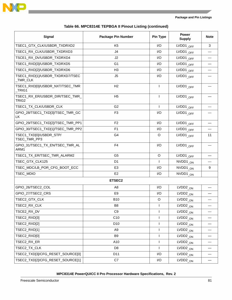
MPC8314E PowerQUICC II Pro Processor Hardware Specifications, Rev. 2
Freescale Semiconductor 81
Package and Pin Listings
TSEC1_GTX_CLK/USBDR_TXDRXD2 K5 I/O LVDD1_OFF 3
TSEC1_RX_CLK/USBDR_TXDRXD3 J4 I/O LVDD1_OFF —
TSCE1_RX_DV/USBDR_TXDRXD4 J2 I/O LVDD1_OFF —
TSEC1_RXD[3]/USBDR_TXDRXD5 G1 I/O LVDD1_OFF —
TSEC1_RXD[2]/USBDR_TXDRXD6 H3 I/O LVDD1_OFF —
TSEC1_RXD[1]/USBDR_TXDRXD7/TSEC_TMR_CLK
J5 I/O LVDD1_OFF —
TSEC1_RXD[0]/USBDR_NXT/TSEC_TMR_TRIG1
H2 I LVDD1_OFF —
TSEC1_RX_ER/USBDR_DIR/TSEC_TMR_TRIG2
H5 I LVDD1_OFF —
TSEC1_TX_CLK/USBDR_CLK G2 I LVDD1_OFF —
GPIO_28/TSEC1_TXD[3]/TSEC_TMR_GCLK
F3 I/O LVDD1_OFF —
GPIO_29/TSEC1_TXD[2]/TSEC_TMR_PP1 F2 I/O LVDD1_OFF —
GPIO_30/TSEC1_TXD[1]/TSEC_TMR_PP2 F1 I/O LVDD1_OFF —
TSEC1_TXD[0]/USBDR_STP/TSEC_TMR_PP3
G4 O LVDD1_OFF 11
GPIO_31/TSEC1_TX_EN/TSEC_TMR_ALARM1
F4 I/O LVDD1_OFF —
TSEC1_TX_ER/TSEC_TMR_ALARM2 G5 O LVDD1_OFF —
TSEC_GTX_CLK125 D1 I NVDD1_ON —
TSEC_MDC/LB_POR_CFG_BOOT_ECC E3 I/O NVDD1_ON 9
TSEC_MDIO E2 I/O NVDD1_ON
ETSEC2
GPIO_26/TSEC2_COL A8 I/O LVDD2_ON —
GPIO_27/TSEC2_CRS E9 I/O LVDD2_ON —
TSEC2_GTX_CLK B10 O LVDD2_ON —
TSEC2_RX_CLK B8 I LVDD2_ON —
TSCE2_RX_DV C9 I LVDD2_ON —
TSEC2_RXD[3] C10 I LVDD2_ON —
TSEC2_RXD[2] D10 I LVDD2_ON —
TSEC2_RXD[1] A9 I LVDD2_ON —
TSEC2_RXD[0] B9 I LVDD2_ON —
TSEC2_RX_ER A10 I LVDD2_ON —
TSEC2_TX_CLK D8 I LVDD2_ON —
TSEC2_TXD[3]/CFG_RESET_SOURCE[0] D11 I/O LVDD2_ON —
TSEC2_TXD[2]/CFG_RESET_SOURCE[1] C7 I/O LVDD2_ON —
Table 66. MPC8314E TEPBGA II Pinout Listing (continued)
Signal Package Pin Number Pin TypePowerSupply
Note

MPC8314E PowerQUICC II Pro Processor Hardware Specifications, Rev. 2
82 Freescale Semiconductor
Package and Pin Listings
TSEC2_TXD[1]/CFG_RESET_SOURCE[2] E8 I/O LVDD2_ON —
TSEC2_TXD[0]/CFG_RESET_SOURCE[3] B7 I/O LVDD2_ON —
TSEC2_TX_EN D12 O LVDD2_ON —
TSEC2_TX_ER B11 O LVDD2_ON —
SGMII / PCI Express PHY
TXA P4 O XPADVDD —
TXA N4 O XPADVDD —
RXA R1 I XCOREVDD —
RXA P1 I XCOREVDD —
TXB U4 O XPADVDD —
TXB V4 O XPADVDD —
RXB U1 I XCOREVDD —
RXB V1 I XCOREVDD —
SD_IMP_CAL_RX N3 I XCOREVDD —
SD_REF_CLK R4 I XCOREVDD —
SD_REF_CLK R5 I XCOREVDD —
SD_PLL_TPD T2 O — —
SD_IMP_CAL_TX V5 I XPADVDD —
SDAVDD T3 I — —
SD_PLL_TPA_ANA T4 O — —
SDAVSS T5 I — —
USB Phy
USB_DP A11 I/O USB_VDDA —
USB_DM A12 I/O USB_VDDA —
USB_VBUS C12 I — —
USB_TPA A14 O — —
USB_RBIAS D14 I — 8
USB_PLL_PWR3 A13 I — —
USB_PLL_GND0 & USB_PLL_GND1 D13 I — —
USB_PLL_PWR1 B13 I — —
USB_VSSA_BIAS E14 I — —
USB_VDDA_BIAS C14 I — —
USB_VSSA E13 I — —
USB_VDDA E12 I — —
GPIO
GPIO_0/DMA_DREQ1/GTM1_TOUT1 C5 I/O NVDD1_ON —
Table 66. MPC8314E TEPBGA II Pinout Listing (continued)
Signal Package Pin Number Pin TypePowerSupply
Note

MPC8314E PowerQUICC II Pro Processor Hardware Specifications, Rev. 2
Freescale Semiconductor 83
Package and Pin Listings
GPIO_1/DMA_DACK1/GTM1_TIN2/GTM2_TIN1
A4 I/O NVDD1_ON —
GPIO_2/DMA_DONE1/GTM1_TGATE2/GTM2_TGATE1
K3 I/O NVDD4_OFF —
GPIO_3/GTM1_TIN3/GTM2_TIN4 K1 I/O NVDD4_OFF —
GPIO_4/GTM1_TGATE3/GTM2_TGATE4 K2 I/O NVDD4_OFF —
GPIO_5/GTM1_TOUT3/GTM2_TOUT1 L5 I/O NVDD4_OFF —
GPIO_6/GTM1_TIN4/GTM2_TIN3 L3 I/O NVDD4_OFF —
GPIO_7/GTM1_TGATE4/GTM2_TGATE3 L1 I/O NVDD4_OFF —
GPIO_8/USBDR_DRIVE_VBUS/GTM1_TIN1/GTM2_TIN2
M1 I/O NVDD4_OFF —
GPIO_9/USBDR_PWRFAULT/GTM1_TGATE1/GTM2_TGATE2
M2 I/O NVDD4_OFF —
GPIO_10/USBDR_PCTL0/GTM1_TOUT2/GTM2_TOUT1
M5 I/O NVDD4_OFF —
GPIO_11/USBDR_PCTL1/GTM1_TOUT4/GTM2_TOUT3
M4 I/O NVDD4_OFF —
SPI
SPIMOSI/GPIO_15 W3 I/O NVDD1_OFF —
SPIMISO/GPIO_16 W4 I/O NVDD1_OFF —
SPICLK Y1 I/O NVDD1_OFF —
SPISEL/GPIO_17 W2 I/O NVDD1_OFF —
Power and Ground Supplies
GVDD Y11, Y12, Y14, Y15, Y17, AC8, AC11, AC14, AC17, AD6, AD9, AD17, AE8,
AE13, AE19, AF10, AF15, AF21, AG2, AG3, AG8, AG13, AG19, AH2
I — —
LVDD1_OFF H6, J3, L6, L9, M9 I — —
LVDD2_ON C11, D9, E10, F11, J12 I — —
NVDD1_OFF U9, V9, W10, Y4, Y6, AA3, AB4
I — —
NVDD1_ON B1, B2, C1, D5, E7, F5, F9, J11, K10 I — —
NVDD2_OFF B22, B27, C19, E16, F15, F18, F21, F25, H25, J17, J18, J23, L20, M20
I — —
NVDD2_ON L26, N19 I — —
NVDD3_OFF U20, V20, V23, V26, W19, Y18, Y26, AA23, AA25, AC20, AC25, AD23, AE25,
AG25, AG27, T27, U27
I — —
NVDD4_OFF K4, L2, M6, N10 I — —
Table 66. MPC8314E TEPBGA II Pinout Listing (continued)
Signal Package Pin Number Pin TypePowerSupply
Note
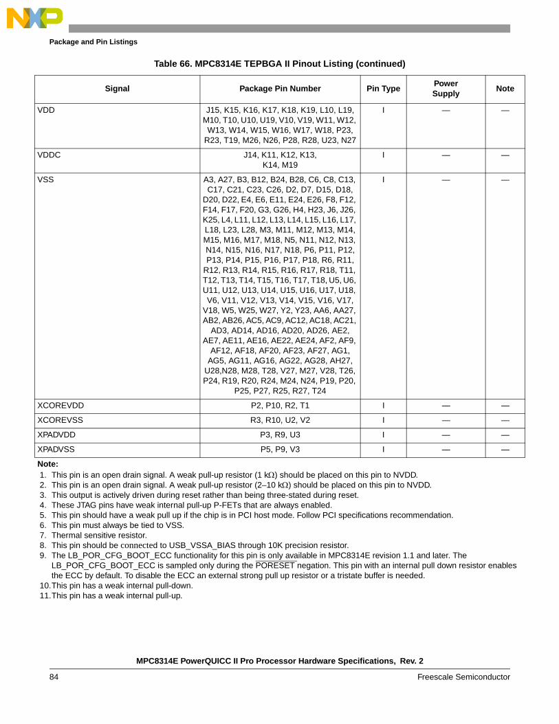
MPC8314E PowerQUICC II Pro Processor Hardware Specifications, Rev. 2
84 Freescale Semiconductor
Package and Pin Listings
VDD J15, K15, K16, K17, K18, K19, L10, L19, M10, T10, U10, U19, V10, V19, W11, W12, W13, W14, W15, W16, W17, W18, P23,
R23, T19, M26, N26, P28, R28, U23, N27
I — —
VDDC J14, K11, K12, K13, K14, M19
I — —
VSS A3, A27, B3, B12, B24, B28, C6, C8, C13, C17, C21, C23, C26, D2, D7, D15, D18,
D20, D22, E4, E6, E11, E24, E26, F8, F12, F14, F17, F20, G3, G26, H4, H23, J6, J26, K25, L4, L11, L12, L13, L14, L15, L16, L17, L18, L23, L28, M3, M11, M12, M13, M14, M15, M16, M17, M18, N5, N11, N12, N13, N14, N15, N16, N17, N18, P6, P11, P12, P13, P14, P15, P16, P17, P18, R6, R11,
R12, R13, R14, R15, R16, R17, R18, T11, T12, T13, T14, T15, T16, T17, T18, U5, U6, U11, U12, U13, U14, U15, U16, U17, U18, V6, V11, V12, V13, V14, V15, V16, V17,
V18, W5, W25, W27, Y2, Y23, AA6, AA27, AB2, AB26, AC5, AC9, AC12, AC18, AC21,
AD3, AD14, AD16, AD20, AD26, AE2, AE7, AE11, AE16, AE22, AE24, AF2, AF9,
AF12, AF18, AF20, AF23, AF27, AG1, AG5, AG11, AG16, AG22, AG28, AH27,
U28,N28, M28, T28, V27, M27, V28, T26, P24, R19, R20, R24, M24, N24, P19, P20,
P25, P27, R25, R27, T24
I — —
XCOREVDD P2, P10, R2, T1 I — —
XCOREVSS R3, R10, U2, V2 I — —
XPADVDD P3, R9, U3 I — —
XPADVSS P5, P9, V3 I — —
Note: 1. This pin is an open drain signal. A weak pull-up resistor (1 k) should be placed on this pin to NVDD.2. This pin is an open drain signal. A weak pull-up resistor (2–10 k) should be placed on this pin to NVDD.3. This output is actively driven during reset rather than being three-stated during reset.4. These JTAG pins have weak internal pull-up P-FETs that are always enabled.5. This pin should have a weak pull up if the chip is in PCI host mode. Follow PCI specifications recommendation.6. This pin must always be tied to VSS.7. Thermal sensitive resistor.8. This pin should be connected to USB_VSSA_BIAS through 10K precision resistor.9. The LB_POR_CFG_BOOT_ECC functionality for this pin is only available in MPC8314E revision 1.1 and later. The
LB_POR_CFG_BOOT_ECC is sampled only during the PORESET negation. This pin with an internal pull down resistor enables the ECC by default. To disable the ECC an external strong pull up resistor or a tristate buffer is needed.
10.This pin has a weak internal pull-down.11.This pin has a weak internal pull-up.
Table 66. MPC8314E TEPBGA II Pinout Listing (continued)
Signal Package Pin Number Pin TypePowerSupply
Note

MPC8314E PowerQUICC II Pro Processor Hardware Specifications, Rev. 2
Freescale Semiconductor 85
Clocking
23 ClockingThis figure shows the internal distribution of clocks within the MPC8314E
1 Multiplication factor M = 1, 1.5, 2, 2.5, and 3. Value is decided by RCWLR[COREPLL].2 Multiplication factor L = 2, 3, 4 and 5. Value is decided by RCWLR[SPMF].
Figure 60. MPC8314E Clock Subsystem
System
LBC
LCLK[0:1]
e300c3 core
csb_clk to rest
csb_clk
Local Bus
PCI_CLK_OUT[0:2]
PCI_SYNC_OUT
PCI_CLK/
ClockUnit
of the device
lbc_clk
_DIV
PCI Clock
PCI_SYNC_IN
MemoryDevice
/n
To local bus Clock
Divider (2) 3
MEMC_MCK
MEMC_MCK
DDR
ddr_clk
DDRMemoryDevice
PLL
to DDRmemorycontroller
Clock
CFG_CLKIN
/2Divider
Divider
10
USB Mac
USB PHYPLL
eTSECProtocol
Converter
GTX_CLK125125-MHz source
SYS_XTAL_IN
SYS_XTAL_OUT
mux
Crystal
SYS_CLK_IN
USB_XTAL_IN
USB_XTAL_OUT
Crystal
USB_CLK_IN
/1,/2
RTC_CLK (32 kHz)
RTC
Sys Ref
Core PLL core_clk
x L2
x M1TDM
/n
PCI ExpressProtocol
Converter
125/100 MHzPLL
PCVTR Mux
SerDes PHY+-
SD_REF_CLK_BSD_REF_CLK
MPC8314E

MPC8314E PowerQUICC II Pro Processor Hardware Specifications, Rev. 2
86 Freescale Semiconductor
Clocking
The primary clock source can be one of two inputs, SYS_CLK_IN or PCI_CLK, depending on whether the device is configured in PCI host or PCI agent mode. When the device is configured as a PCI host device, SYS_CLK_IN is its primary input clock. SYS_CLK_IN feeds the PCI clock divider (2) and the multiplexors for PCI_SYNC_OUT and PCI_CLK_OUT. The CFG_SYS_CLKIN_DIV configuration input selects whether SYS_CLK_IN or SYS_CLK_IN/2 is driven out on the PCI_SYNC_OUT signal.
PCI_SYNC_OUT is connected externally to PCI_SYNC_IN to allow the internal clock subsystem to synchronize to the system PCI clocks. PCI_SYNC_OUT must be connected properly to PCI_SYNC_IN, with equal delay to all PCI agent devices in the system, to allow the device to function. When the device is configured as a PCI agent device, PCI_CLK is the primary input clock. When the device is configured as a PCI agent device the SYS_CLK_IN signal should be tied to GND.
As shown in Figure 60, the primary clock input (frequency) is multiplied up by the system phase-locked loop (PLL) and the clock unit to create the coherent system bus clock (csb_clk), the internal clock for the DDR controller (ddr_clk), and the internal clock for the local bus interface unit (lbiu_clk).
The csb_clk frequency is derived from a complex set of factors that can be simplified into the following equation:
csb_clk = {PCI_SYNC_IN × (1 + ~ CFG_SYS_CLKIN_DIV)} × SPMF
In PCI host mode, PCI_SYNC_IN × (1 + ~ CFG_SYS_CLKIN_DIV) is the SYS_CLK_IN frequency.
The csb_clk serves as the clock input to the e300 core. A second PLL inside the e300 core multiplies up the csb_clk frequency to create the internal clock for the e300 core (core_clk). The system and core PLL multipliers are selected by the SPMF and COREPLL fields in the reset configuration word low (RCWL) which is loaded at power-on reset or by one of the hard-coded reset options. See Chapter 4, “Reset, Clocking, and Initialization,” in the MPC8315E PowerQUICC II Pro Integrated Host Processor Family Reference Manual for more information on the clock subsystem.
The internal ddr_clk frequency is determined by the following equation:
ddr_clk = csb_clk × (1 + RCWL[DDRCM])
Note that ddr_clk is not the external memory bus frequency; ddr_clk passes through the DDR clock divider (2) to create the differential DDR memory bus clock outputs (MCK and MCK). However, the data rate is the same frequency as ddr_clk.
The internal lbiu_clk frequency is determined by the following equation:
lbiu_clk = csb_clk × (1 + RCWL[LBCM])
Note that lbiu_clk is not the external local bus frequency; lbiu_clk passes through the LBIU clock divider to create the external local bus clock outputs (LCLK[0:1]). The LBIU clock divider ratio is controlled by LCRR[CLKDIV].
In addition, some of the internal units may be required to be shut off or operate at lower frequency than the csb_clk frequency. Those units have a default clock ratio that can be configured by a memory mapped register after the device comes out of reset. Table 67 specifies which units have a configurable clock frequency.
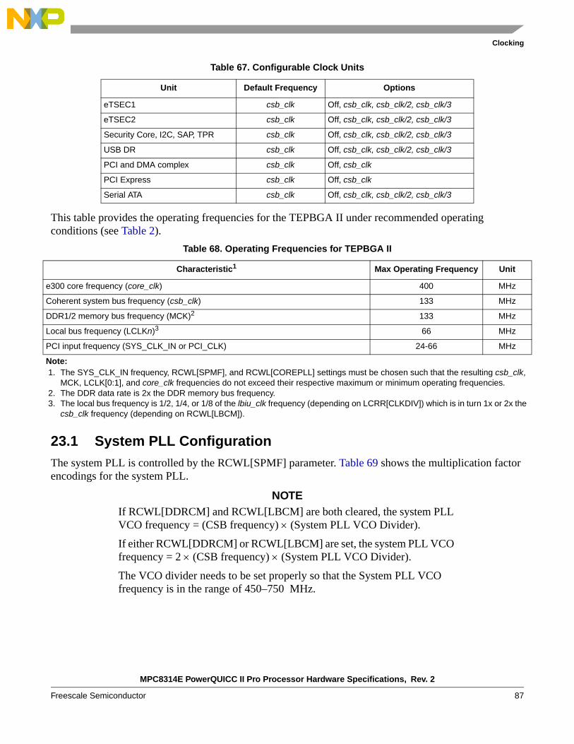
MPC8314E PowerQUICC II Pro Processor Hardware Specifications, Rev. 2
Freescale Semiconductor 87
Clocking
This table provides the operating frequencies for the TEPBGA II under recommended operating conditions (see Table 2).
23.1 System PLL Configuration The system PLL is controlled by the RCWL[SPMF] parameter. Table 69 shows the multiplication factor encodings for the system PLL.
NOTEIf RCWL[DDRCM] and RCWL[LBCM] are both cleared, the system PLL VCO frequency = (CSB frequency) (System PLL VCO Divider).
If either RCWL[DDRCM] or RCWL[LBCM] are set, the system PLL VCO frequency = 2 (CSB frequency) (System PLL VCO Divider).
The VCO divider needs to be set properly so that the System PLL VCO frequency is in the range of 450–750 MHz.
Table 67. Configurable Clock Units
Unit Default Frequency Options
eTSEC1 csb_clk Off, csb_clk, csb_clk/2, csb_clk/3
eTSEC2 csb_clk Off, csb_clk, csb_clk/2, csb_clk/3
Security Core, I2C, SAP, TPR csb_clk Off, csb_clk, csb_clk/2, csb_clk/3
USB DR csb_clk Off, csb_clk, csb_clk/2, csb_clk/3
PCI and DMA complex csb_clk Off, csb_clk
PCI Express csb_clk Off, csb_clk
Serial ATA csb_clk Off, csb_clk, csb_clk/2, csb_clk/3
Table 68. Operating Frequencies for TEPBGA II
Characteristic1 Max Operating Frequency Unit
e300 core frequency (core_clk) 400 MHz
Coherent system bus frequency (csb_clk) 133 MHz
DDR1/2 memory bus frequency (MCK)2 133 MHz
Local bus frequency (LCLKn)3 66 MHz
PCI input frequency (SYS_CLK_IN or PCI_CLK) 24-66 MHz
Note: 1. The SYS_CLK_IN frequency, RCWL[SPMF], and RCWL[COREPLL] settings must be chosen such that the resulting csb_clk,
MCK, LCLK[0:1], and core_clk frequencies do not exceed their respective maximum or minimum operating frequencies. 2. The DDR data rate is 2x the DDR memory bus frequency.3. The local bus frequency is 1/2, 1/4, or 1/8 of the lbiu_clk frequency (depending on LCRR[CLKDIV]) which is in turn 1x or 2x the
csb_clk frequency (depending on RCWL[LBCM]).

MPC8314E PowerQUICC II Pro Processor Hardware Specifications, Rev. 2
88 Freescale Semiconductor
Clocking
As described in Section 23, “Clocking,” The LBCM, DDRCM, and SPMF parameters in the reset configuration word low and the CFG_SYS_CLKIN_DIV configuration input signal select the ratio between the primary clock input (SYS_CLK_IN or PCI_CLK) and the internal coherent system bus clock (csb_clk). Table 70 and Table 71 shows the expected frequency values for the CSB frequency for select csb_clk to SYS_CLK_IN/PCI_SYNC_IN ratios.
Table 69. System PLL Multiplication Factors
RCWL[SPMF]System PLL
Multiplication Factor
0000 Reserved
0001 Reserved
0010 2
0011 3
0100 4
0101 5
0110–1111 Reserved
Table 70. CSB Frequency Options for Host Mode
CFG_SYS_CLKIN_DIVat Reset1
1 CFG_SYS_CLKIN_DIV select the ratio between SYS_CLK_IN and PCI_SYNC_OUT.
SPMFcsb_clk :
Input Clock Ratio 2
2 SYS_CLK_IN is the input clock in host mode; PCI_CLK is the input clock in agent mode.
Input ClockFrequency (MHz)2
24 33.33 66.67
High/Low 3
3 In the Host mode it does not matter if the value is High or Low.
0010 2:1 133
High/Low 0011 3:1 100 —
High/Low 0100 4:1 96 133 —
High/Low 0101 5:1 120 — —
Table 71. CSB Frequency Options for Agent Mode
CFG_SYS_CLKIN_DIVat Reset1
1 CFG_SYS_CLKIN_DIV doubles csb_clk if set low.
SPMFcsb_clk :
Input Clock Ratio 2
2 SYS_CLK_IN is the input clock in host mode; PCI_CLK is the input clock in agent mode.
Input Clockfrequency (MHz)2
25 33.33 66.67
High 0010 2: 1 133
High 0011 3: 1 100 —
High 0100 4: 1 133 —
High 0101 5: 1 120 — —

MPC8314E PowerQUICC II Pro Processor Hardware Specifications, Rev. 2
Freescale Semiconductor 89
Clocking
23.2 Core PLL ConfigurationRCWL[COREPLL] selects the ratio between the internal coherent system bus clock (csb_clk) and the e300 core clock (core_clk). Table 72 shows the encodings for RCWL[COREPLL]. COREPLL values that are not listed in Table 72 should be considered as reserved.
NOTECore VCO frequency = core frequency VCO dividerVCO divider has to be set properly so that the core VCO frequency is in the range of 400–800 MHz.
23.3 Suggested PLL ConfigurationsTo simplify the PLL configurations, the MPC8314E might be separated into two clock domains. The first domain contain the CSB PLL and the core PLL. The core PLL is connected serially to the CSB PLL, and has the csb_clk as its input clock. The clock domains are independent, and each of their PLLs are configured separately. Both of the domains has one common input clock. Table 73 shows suggested PLL configurations for 33, 25, and 66 MHz input clocks.
Table 72. e300 Core PLL Configuration
RCWL[COREPLL]core_clk : csb_clk Ratio VCO Divider1
1 Core VCO frequency = core frequency VCO divider.
0–1 2–5 6
nn 0000 0 PLL bypassed (PLL off, csb_clk clocks core directly)
PLL bypassed (PLL off, csb_clk clocks core directly)
11 nnnn n N/A N/A
00 0001 0 1:1 2
01 0001 0 1:1 4
00 0001 1 1.5:1 2
01 0001 1 1.5:1 4
00 0010 0 2:1 2
01 0010 0 2:1 4
00 0010 1 2.5:1 2
01 0010 1 2.5:1 4
00 0011 0 3:1 2
01 0011 0 3:1 4
Table 73. Suggested PLL Configurations
Conf. No. SPMF Core\PLL Input Clock Frequency (MHz) CSB Frequency (MHz) Core Frequency (MHz)
1 0100 0000100 33.33 133.33 266.66
3 0010 0000100 66.67 133.33 266.66
4 0100 0000101 33.33 133.33 333.33
5 0101 0000101 25 125 312.5
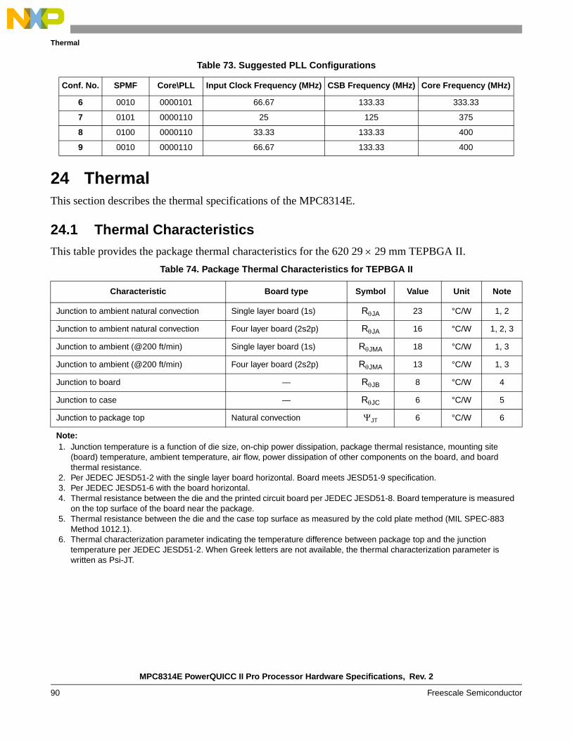
MPC8314E PowerQUICC II Pro Processor Hardware Specifications, Rev. 2
90 Freescale Semiconductor
Thermal
24 ThermalThis section describes the thermal specifications of the MPC8314E.
24.1 Thermal CharacteristicsThis table provides the package thermal characteristics for the 620 29 29 mm TEPBGA II.
6 0010 0000101 66.67 133.33 333.33
7 0101 0000110 25 125 375
8 0100 0000110 33.33 133.33 400
9 0010 0000110 66.67 133.33 400
Table 74. Package Thermal Characteristics for TEPBGA II
Characteristic Board type Symbol Value Unit Note
Junction to ambient natural convection Single layer board (1s) RJA 23 °C/W 1, 2
Junction to ambient natural convection Four layer board (2s2p) RJA 16 °C/W 1, 2, 3
Junction to ambient (@200 ft/min) Single layer board (1s) RJMA 18 °C/W 1, 3
Junction to ambient (@200 ft/min) Four layer board (2s2p) RJMA 13 °C/W 1, 3
Junction to board — RJB 8 °C/W 4
Junction to case — RJC 6 °C/W 5
Junction to package top Natural convection JT 6 °C/W 6
Note: 1. Junction temperature is a function of die size, on-chip power dissipation, package thermal resistance, mounting site
(board) temperature, ambient temperature, air flow, power dissipation of other components on the board, and board thermal resistance.
2. Per JEDEC JESD51-2 with the single layer board horizontal. Board meets JESD51-9 specification.3. Per JEDEC JESD51-6 with the board horizontal.4. Thermal resistance between the die and the printed circuit board per JEDEC JESD51-8. Board temperature is measured
on the top surface of the board near the package.5. Thermal resistance between the die and the case top surface as measured by the cold plate method (MIL SPEC-883
Method 1012.1).6. Thermal characterization parameter indicating the temperature difference between package top and the junction
temperature per JEDEC JESD51-2. When Greek letters are not available, the thermal characterization parameter is written as Psi-JT.
Table 73. Suggested PLL Configurations
Conf. No. SPMF Core\PLL Input Clock Frequency (MHz) CSB Frequency (MHz) Core Frequency (MHz)

MPC8314E PowerQUICC II Pro Processor Hardware Specifications, Rev. 2
Freescale Semiconductor 91
Thermal
24.2 Thermal Management InformationFor the following sections, PD = (VDD IDD) + PI/O where PI/O is the power dissipation of the I/O drivers.
24.2.1 Estimation of Junction Temperature with Junction-to-Ambient Thermal Resistance
An estimation of the chip junction temperature, TJ, can be obtained from the equation:
TJ = TA + (RJA PD)
where:
TJ = junction temperature (C)
TA = ambient temperature for the package (C)
RJA = junction to ambient thermal resistance (C/W)
PD = power dissipation in the package (W)
The junction to ambient thermal resistance is an industry standard value that provides a quick and easy estimation of thermal performance. As a general statement, the value obtained on a single layer board is appropriate for a tightly packed printed circuit board. The value obtained on the board with the internal planes is usually appropriate if the board has low power dissipation and the components are well separated. Test cases have demonstrated that errors of a factor of two (in the quantity TJ - TA) are possible.
24.2.2 Estimation of Junction Temperature with Junction-to-Board Thermal Resistance
The thermal performance of a device cannot be adequately predicted from the junction to ambient thermal resistance. The thermal performance of any component is strongly dependent on the power dissipation of surrounding components. In addition, the ambient temperature varies widely within the application. For many natural convection and especially closed box applications, the board temperature at the perimeter (edge) of the package is approximately the same as the local air temperature near the device. Specifying the local ambient conditions explicitly as the board temperature provides a more precise description of the local ambient conditions that determine the temperature of the device.
At a known board temperature, the junction temperature is estimated using the following equation:
TJ = TB + (RJB PD)
where:
TJ = junction temperature (C)
TB = board temperature at the package perimeter (C)
RJB = junction to board thermal resistance (C/W) per JESD51-8
PD = power dissipation in the package (W)
When the heat loss from the package case to the air can be ignored, acceptable predictions of junction temperature can be made. The application board should be similar to the thermal test condition: the component is soldered to a board with internal planes.

MPC8314E PowerQUICC II Pro Processor Hardware Specifications, Rev. 2
92 Freescale Semiconductor
Thermal
24.2.3 Experimental Determination of Junction Temperature
To determine the junction temperature of the device in the application after prototypes are available, the Thermal Characterization Parameter (JT) can be used to determine the junction temperature with a measurement of the temperature at the top center of the package case using the following equation:
TJ = TT + (JT PD)
where:
TJ = junction temperature (C)
TT = thermocouple temperature on top of package (C)
JT = junction to ambient thermal resistance (C/W)
PD = power dissipation in the package (W)
The thermal characterization parameter is measured per JESD51-2 specification using a 40 gauge type T thermocouple epoxied to the top center of the package case. The thermocouple should be positioned so that the thermocouple junction rests on the package. A small amount of epoxy is placed over the thermocouple junction and over about 1 mm of wire extending from the junction. The thermocouple wire is placed flat against the package case to avoid measurement errors caused by cooling effects of the thermocouple wire.
24.2.4 Heat Sinks and Junction-to-Case Thermal Resistance
In some application environments, a heat sink is required to provide the necessary thermal management of the device. When a heat sink is used, the thermal resistance is expressed as the sum of a junction to case thermal resistance and a case to ambient thermal resistance:
RJA = RJC + RCA
where:
RJA = junction to ambient thermal resistance (C/W)
RJC = junction to case thermal resistance (C/W)
RCA = case to ambient thermal resistance (C/W)
RJC is device related and cannot be influenced by the user. The user controls the thermal environment to change the case to ambient thermal resistance, RCA. For instance, the user can change the size of the heat sink, the air flow around the device, the interface material, the mounting arrangement on printed circuit board, or change the thermal dissipation on the printed circuit board surrounding the device.
To illustrate the thermal performance of the devices with heat sinks, the thermal performance has been simulated with a few commercially available heat sinks. The heat sink choice is determined by the application environment (temperature, air flow, adjacent component power dissipation) and the physical space available. Because there is not a standard application environment, a standard heat sink is not required.

MPC8314E PowerQUICC II Pro Processor Hardware Specifications, Rev. 2
Freescale Semiconductor 93
Thermal
Accurate thermal design requires thermal modeling of the application environment using computational fluid dynamics software which can model both the conduction cooling and the convection cooling of the air moving through the application. Simplified thermal models of the packages can be assembled using the junction-to-case and junction-to-board thermal resistances listed in the thermal resistance table. More detailed thermal models can be made available on request.
Heat sink vendors include the following list:
Aavid Thermalloy 603-224-998880 Commercial St.Concord, NH 03301Internet: www.aavidthermalloy.com
Alpha Novatech 408-749-7601473 Sapena Ct. #12Santa Clara, CA 95054Internet: www.alphanovatech.com
International Electronic Research Corporation (IERC) 818-842-7277413 North Moss St.Burbank, CA 91502Internet: www.ctscorp.com
Table 75. Heat Sinks and Junction-to-Case Thermal Resistance of MPC8314E TEPBGA II
Heat Sink Assuming Thermal Grease Air Flow
29 29 mm TEBGA II
Junction-to-Ambient Thermal Resistance
AAVID 30 x 30 x 9.4 mm Pin Fin Natural Convection 14.4
AAVID 30 x 30 x 9.4 mm Pin Fin 0.5 m/s 11.4
AAVID 30 x 30 x 9.4 mm Pin Fin 1 m/s 10.1
AAVID 30 x 30 x 9.4 mm Pin Fin 2 m/s 8.9
AAVID 35 x 31 x 23 mm Pin Fin Natural Convection 12.3
AAVID 35 x 31 x 23 mm Pin Fin 0.5 m/s 9.3
AAVID 35 x 31 x 23 mm Pin Fin 1 m/s 8.5
AAVID 35 x 31 x 23 mm Pin Fin 2 m/s 7.9
AAVID 43 x 41 x 16.5 mm Pin Fin Natural Convection 12.5
AAVID 43 x 41 x 16.5 mm Pin Fin 0.5 m/s 9.7
AAVID 43 x 41 x 16.5 mm Pin Fin 1 m/s 8.5
AAVID 43 x 41 x 16.5 mm Pin Fin 2 m/s 7.7
Wakefield, 53 x 53 x 25 mm Pin Fin Natural Convection 10.9
Wakefield, 53 x 53 x 25 mm Pin Fin 0.5 m/s 8.5
Wakefield, 53 x 53 x 25 mm Pin Fin 1 m/s 7.5
Wakefield, 53 x 53 x 25 mm Pin Fin 2 m/s 7.1

MPC8314E PowerQUICC II Pro Processor Hardware Specifications, Rev. 2
94 Freescale Semiconductor
Thermal
Millennium Electronics (MEI) 408-436-8770Loroco Sites671 East Brokaw RoadSan Jose, CA 95112Internet: www.mei-thermal.com
Tyco Electronics 800-522-6752Chip Coolers™P.O. Box 3668Harrisburg, PA 17105Internet: www.tycoelectronics.com
Wakefield Engineering 603-635-280033 Bridge St.Pelham, NH 03076Internet: www.wakefield.com
Interface material vendors include the following:
Chomerics, Inc. 781-935-485077 Dragon Ct.Woburn, MA 01801Internet: www.chomerics.com
Dow-Corning Corporation 800-248-2481Corporate Center
PO BOX 994
Midland, MI 48686-0994Internet: www.dowcorning.com
Shin-Etsu MicroSi, Inc. 888-642-767410028 S. 51st St.Phoenix, AZ 85044Internet: www.microsi.com
The Bergquist Company 800-347-457218930 West 78th St.Chanhassen, MN 55317Internet: www.bergquistcompany.com
24.3 Heat Sink AttachmentWhen attaching heat sinks to these devices, an interface material is required. The best method is to use thermal grease and a spring clip. The spring clip should connect to the printed circuit board, either to the board itself, to hooks soldered to the board, or to a plastic stiffener. Avoid attachment forces which would lift the edge of the package or peel the package from the board. Such peeling forces reduce the solder joint lifetime of the package. Recommended maximum force on the top of the package is 10 lb force (45 Newtons). If an adhesive attachment is planned, the adhesive should be intended for attachment to painted or plastic surfaces and its performance verified under the application requirements.

MPC8314E PowerQUICC II Pro Processor Hardware Specifications, Rev. 2
Freescale Semiconductor 95
System Design Information
24.3.1 Experimental Determination of the Junction Temperature with a Heat Sink
When heat sink is used, the junction temperature is determined from a thermocouple inserted at the interface between the case of the package and the interface material. A clearance slot or hole is normally required in the heat sink. Minimizing the size of the clearance is important to minimize the change in thermal performance caused by removing part of the thermal interface to the heat sink temperature and then back calculate the case temperature using a separate measurement of the thermal resistance of the interface. From this case temperature, the junction temperature is determined from the junction to case thermal resistance.
TJ = TC + (RJC x PD)
Where
TC is the case temperature of the package
RJC is the junction-to-case thermal resistance
PD is the power dissipation
25 System Design InformationThis section provides electrical and thermal design recommendations for successful application of the MPC8314E.
25.1 System ClockingThe MPC8314E includes two PLLs.
1. The platform PLL (AVDD2) generates the platform clock from the externally supplied SYS_CLK_IN input. The frequency ratio between the platform and SYS_CLK_IN is selected using the platform PLL ratio configuration bits as described in Section 23.1, “System PLL Configuration.”
2. The e300 Core PLL (AVDD1) generates the core clock as a slave to the platform clock. The frequency ratio between the e300 core clock and the platform clock is selected using the e300 PLL ratio configuration bits as described in Section 23.2, “Core PLL Configuration.”
25.2 PLL Power Supply FilteringEach of the PLLs listed above is provided with power through independent power supply pins (AVDD1,AVDD2 respectively). The AVDD level should always be equivalent to VDD, and preferably these voltages are derived directly from VDD through a low frequency filter scheme such as the following.
There are a number of ways to reliably provide power to the PLLs, but the recommended solution is to provide independent filter circuits as illustrated in Figure 61, one to each of the AVDD pins. By providing independent filters to each PLL the opportunity to cause noise injection from one PLL to the other is reduced.

MPC8314E PowerQUICC II Pro Processor Hardware Specifications, Rev. 2
96 Freescale Semiconductor
System Design Information
This circuit is intended to filter noise in the PLLs resonant frequency range from a 500 kHz to 10 MHz range. It should be built with surface mount capacitors with minimum Effective Series Inductance (ESL). Consistent with the recommendations of Dr. Howard Johnson in High Speed Digital Design: A Handbook of Black Magic (Prentice Hall, 1993), multiple small capacitors of equal value are recommended over a single large value capacitor.
Each circuit should be placed as close as possible to the specific AVDD pin being supplied to minimize noise coupled from nearby circuits. It should be possible to route directly from the capacitors to the AVDD pin, which is on the periphery of package, without the inductance of vias. Note that the RC filter results in lower voltage level on AVDD. This does not imply that the DC specification can be relaxed.
This figure shows the PLL power supply filter circuit.
Figure 61. PLL Power Supply Filter Circuit
25.3 Decoupling RecommendationsDue to large address and data buses, and high operating frequencies, the device can generate transient power surges and high frequency noise in its power supply, especially while driving large capacitive loads. This noise must be prevented from reaching other components in the MPC8314E system, and the MPC8314E itself requires a clean, tightly regulated source of power. Therefore, it is recommended that the system designer place at least one decoupling capacitor at each VDD, NVDD, GVDD, and LVDD pins of the device. These decoupling capacitors should receive their power from separate VDD, NVDD, GVDD, LVDD, and GND power planes in the PCB, utilizing thick and short traces to minimize inductance. Capacitors may be placed directly under the device using a standard escape pattern. Others may surround the part.
These capacitors should have a value of 0.01 or 0.1 µF. Only ceramic SMT (surface mount technology) capacitors should be used to minimize lead inductance, preferably 0402 or 0603 sizes.
In addition, it is recommended that there be several bulk storage capacitors distributed around the PCB, feeding the VDD, NVDD, GVDD, and LVDD planes, to enable quick recharging of the smaller chip capacitors. These bulk capacitors should have a low ESR (equivalent series resistance) rating to ensure the quick response time necessary. They should also be connected to the power and ground planes through two vias to minimize inductance. Suggested bulk capacitors—100–330 µF (AVX TPS tantalum or Sanyo OSCON).
25.4 Connection RecommendationsTo ensure reliable operation, it is highly recommended to connect unused inputs to an appropriate signal level. Unused active low inputs should be tied to NVDD, GVDD, or LVDD as required. Unused active high inputs should be connected to GND. All NC (no-connect) signals must remain unconnected.
VDD AVDD (or L2AVDD)
2.2 µF 2.2 µF
GNDLow ESL Surface Mount Capacitors
10

MPC8314E PowerQUICC II Pro Processor Hardware Specifications, Rev. 2
Freescale Semiconductor 97
System Design Information
Power and ground connections must be made to all external VDD, GVDD, LVDD, NVDD, and GND pins of the device.
25.5 Output Buffer DC ImpedanceThe MPC8314E drivers are characterized over process, voltage, and temperature. For all buses, the driver is a push-pull single-ended driver type (open drain for I2C).
To measure Z0 for the single-ended drivers, an external resistor is connected from the chip pad to NVDD or GND. Then, the value of each resistor is varied until the pad voltage is NVDD/2 (see Figure 62). The output impedance is the average of two components, the resistances of the pull-up and pull-down devices. When data is held high, SW1 is closed (SW2 is open) and RP is trimmed until the voltage at the pad equals NVDD/2. RP then becomes the resistance of the pull-up devices. RP and RN are designed to be close to each other in value. Then, Z0 = (RP + RN)/2.
Figure 62. Driver Impedance Measurement
The value of this resistance and the strength of the driver’s current source can be found by making two measurements. First, the output voltage is measured while driving logic 1 without an external differential termination resistor. The measured voltage is V1 = Rsource Isource. Second, the output voltage is measured while driving logic 1 with an external precision differential termination resistor of value Rterm. The measured voltage is V2 = (1/(1/R1 + 1/R2)) Isource. Solving for the output impedance gives Rsource = Rterm (V1/V2 – 1). The drive current is then Isource = V1/Rsource.
NVDD
OGND
RP
RN
PadData
SW1
SW2

MPC8314E PowerQUICC II Pro Processor Hardware Specifications, Rev. 2
98 Freescale Semiconductor
Ordering Information
This table summarizes the signal impedance targets. The driver impedance are targeted at minimum VDD, nominal NVDD, 105C.
25.6 Configuration Pin MultiplexingThe MPC8314E provides the user with power-on configuration options that can be set through the use of external pull-up or pull-down resistors of 4.7 k on certain output pins (see customer visible configuration pins). These pins are generally used as output only pins in normal operation.
While HRESET is asserted however, these pins are treated as inputs. The value presented on these pins while HRESET is asserted, is latched when PORESET deasserts, at which time the input receiver is disabled and the I/O circuit takes on its normal function. Careful board layout with stubless connections to these pull-up/pull-down resistors coupled with the large value of the pull-up/pull-down resistor should minimize the disruption of signal quality or speed for output pins thus configured.
25.7 Pull-Up Resistor RequirementsThe MPC8314E requires high resistance pull-up resistors (10 k is recommended) on open drain type pins including I2C pins and EPIC interrupt pins.
For more information on required pull up resistors and the connections required for JTAG interface, see AN3438, MPC8315 Design Checklist
26 Ordering InformationOrdering information for the parts fully covered by this specification document is provided in Section 26.1, “Part Numbers Fully Addressed by this Document.”
26.1 Part Numbers Fully Addressed by this DocumentThis table provides the Freescale part numbering nomenclature for the MPC8314E. Note that the individual part numbers correspond to a maximum processor core frequency. For available frequencies, contact your local Freescale sales office. In addition to the processor frequency, the part numbering scheme
Table 76. Impedance Characteristics
Impedance
Local Bus, Ethernet, DUART, Control,
Configuration, Power Management
PCI Signals(not including PCI
Output Clocks)
PCI Output Clocks(including
PCI_SYNC_OUT) DDR DRAM Symbol Unit
RN 42 Target 25 Target 42 Target 20 Target Z0
RP 42 Target 25 Target 42 Target 20 Target Z0
Differential NA NA NA NA ZDIFF
Note: Nominal supply voltages. See Table 1, Tj = 105C.
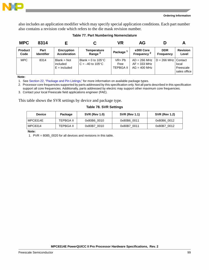
MPC8314E PowerQUICC II Pro Processor Hardware Specifications, Rev. 2
Freescale Semiconductor 99
Ordering Information
also includes an application modifier which may specify special application conditions. Each part number also contains a revision code which refers to the die mask revision number.
This table shows the SVR settings by device and package type.
Table 77. Part Numbering Nomenclature
MPC 8314 E C VR AG D A
ProductCode
PartIdentifier
Encryption Acceleration
Temperature Range 3
Package 1e300 Core
Frequency 2DDR
FrequencyRevision
Level
MPC 8314 Blank = Not includedE = included
Blank = 0 to 105CC = –40 to 105C
VR= Pb Free
TEPBGA II
AD = 266 MHzAF = 333 MHzAG = 400 MHz
D = 266 MHz Contact local Freescale sales office
Note: 1. See Section 22, “Package and Pin Listings,” for more information on available package types.2. Processor core frequencies supported by parts addressed by this specification only. Not all parts described in this specification
support all core frequencies. Additionally, parts addressed by electric may support other maximum core frequencies.3. Contact your local Freescale field applications engineer (FAE).
Table 78. SVR Settings
Device Package SVR (Rev 1.0) SVR (Rev 1.1) SVR (Rev 1.2)
MPC8314E TEPBGA II 0x80B6_0010 0x80B6_0011 0x80B6_0012
MPC8314 TEPBGA II 0x80B7_0010 0x80B7_0011 0x80B7_0012
Note: 1. PVR = 8085_0020 for all devices and revisions in this table.

MPC8314E PowerQUICC II Pro Processor Hardware Specifications, Rev. 2
100 Freescale Semiconductor
Revision History
27 Revision HistoryThis table summarizes a revision history for this document.
Table 79. Revision History
Revision Date Substantive Change(s)
2 11/2011 • In Table 66: – Corrected Note 10 to pull down.– Added pull up information.
1 11/2011 • Added Notes 4, 5, 6, and 7 in Table 2. • In Table 6:
– Decoupled PCI_CLK and SYS_CLK_IN rise and fall times.– Relaxed maximum rise/fall time of SYS_CLK_IN from 1.2 ns to 4 ns.– Modified Note 2.– Updated SYS_CLK_IN/PCI_CLK frequency from 66 MHz to 66.67 MHz.
• Added Note 4 to Table 9. • Added a note stating “eTSEC should be interfaced with peripheral operating at same voltage level.”
in Section 9.1.1, “MII, RMII, RGMII, and RTBI DC Electrical Characteristics.” • Added a note in Table 26 stating “The frequency of RX_CLK should not exceed the TX_CLK by
more than 300 ppm." • Added a note in Table 29 stating “The frequency of RX_CLK should not exceed the GTX_CLK125
by more than 300 ppm • In Table 42, changed min/max values of tCLK_TOL from 0.05 to 0.005. • Added tLALEHOV parameter to Table 44 • Replaced 50 with 50 in Section 16.5, “Receiver Compliance Eye Diagrams.” • In Table 66:
– Added Pull up and Pull down information.– Removed Note 2 from TSEC_MDIO.
• Removed configuration 2 from Table 73. • Removed Preliminary from Section 24, “Thermal.” • Removed MDIO signal from Section 25.7, “Pull-Up Resistor Requirements” as this signal is not
open drain. • Replaced LCCR with LCRR throughout. • Replaced SYS_CLKIN with SYS_CLK_IN throughout. • Replaced all LBIUCM with LBCM. • Replaced all SYS_CR_CLK_IN and SYS_CR_CLK_OUT with SYS_XTAL_IN and
SYS_XTAL_OUT, respectively. Replaced all USB_CR_CLK_IN and USB_CR_CLK_OUT with USB_XTAL_IN and USB_XTAL_OUT, respectively.
• Added rise/fall time spec for TDM CLK
0 05/2009 Initial public release

Document Number: MPC8314EECRev. 211/2011
Information in this document is provided solely to enable system and software
implementers to use Freescale Semiconductor products. There are no express or
implied copyright licenses granted hereunder to design or fabricate any integrated
circuits or integrated circuits based on the information in this document.
Freescale Semiconductor reserves the right to make changes without further notice to
any products herein. Freescale Semiconductor makes no warranty, representation or
guarantee regarding the suitability of its products for any particular purpose, nor does
Freescale Semiconductor assume any liability arising out of the application or use of
any product or circuit, and specifically disclaims any and all liability, including without
limitation consequential or incidental damages. “Typical” parameters which may be
provided in Freescale Semiconductor data sheets and/or specifications can and do
vary in different applications and actual performance may vary over time. All operating
parameters, including “Typicals” must be validated for each customer application by
customer’s technical experts. Freescale Semiconductor does not convey any license
under its patent rights nor the rights of others. Freescale Semiconductor products are
not designed, intended, or authorized for use as components in systems intended for
surgical implant into the body, or other applications intended to support or sustain life,
or for any other application in which the failure of the Freescale Semiconductor product
could create a situation where personal injury or death may occur. Should Buyer
purchase or use Freescale Semiconductor products for any such unintended or
unauthorized application, Buyer shall indemnify and hold Freescale Semiconductor
and its officers, employees, subsidiaries, affiliates, and distributors harmless against all
claims, costs, damages, and expenses, and reasonable attorney fees arising out of,
directly or indirectly, any claim of personal injury or death associated with such
unintended or unauthorized use, even if such claim alleges that Freescale
Semiconductor was negligent regarding the design or manufacture of the part.
How to Reach Us:
Home Page: www.freescale.com
Web Support: http://www.freescale.com/support
USA/Europe or Locations Not Listed: Freescale Semiconductor, Inc.Technical Information Center, EL5162100 East Elliot Road Tempe, Arizona 85284 1-800-521-6274 or+1-480-768-2130www.freescale.com/support
Europe, Middle East, and Africa:Freescale Halbleiter Deutschland GmbHTechnical Information CenterSchatzbogen 781829 Muenchen, Germany+44 1296 380 456 (English) +46 8 52200080 (English)+49 89 92103 559 (German)+33 1 69 35 48 48 (French) www.freescale.com/support
Japan: Freescale Semiconductor Japan Ltd. HeadquartersARCO Tower 15F1-8-1, Shimo-Meguro, Meguro-ku Tokyo 153-0064Japan 0120 191014 or+81 3 5437 [email protected]
Asia/Pacific: Freescale Semiconductor China Ltd. Exchange Building 23FNo. 118 Jianguo RoadChaoyang DistrictBeijing 100022China+86 10 5879 [email protected]
For Literature Requests Only:Freescale Semiconductor
Literature Distribution Center 1-800 441-2447 or+1-303-675-2140Fax: +1-303-675-2150LDCForFreescaleSemiconductor
@hibbertgroup.com
Freescale and the Freescale logo are trademarks of Freescale Semiconductor, Inc. Reg. U.S. Pat. & Tm. Off. QorIQ is a trademark of Freescale Semiconductor, Inc. All other product or service names are the property of their respective owners. The Power Architecture and Power.org word marks and the Power and Power.org logos and related marks are trademarks and service marks licensed by Power.org. © 2011 Freescale Semiconductor, Inc.