MOSFETs in ICs—Scaling, Leakage, and Other Topicshu/Chenming-Hu_ch7.pdf260 Chapter 7 MOSFETs in...
32
259 7 MOSFETs in ICs—Scaling, Leakage, and Other Topics CHAPTER OBJECTIVES How the MOSFET gate length might continue to be reduced is the subject of this chap- ter. One important topic is the off-state current or the leakage current of the MOSFETs. This topic complements the discourse on the on-state current conducted in the previ- ous chapter. The major topics covered here are the subthreshold leakage and its impact on device size reduction, the trade-off between I on and I off and the effects on circuit design. Special emphasis is placed on the understanding of the opportunities for future MOSFET scaling including mobility enhancement, high-k dielectric and metal gate, SOI, multigate MOSFET, metal source/drain, etc. Device simulation and MOSFET compact model for circuit simulation are also introduced. etal–oxide–semiconductor (MOS) integrated circuits (ICs) have met the world’s growing needs for electronic devices for computing, communication, entertainment, automotive, and other applications with continual improvements in cost, speed, and power consumption. These improvements in turn stimulated and enabled new applications and greatly improved the quality of life and productivity worldwide. 7.1 TECHNOLOGY SCALING—FOR COST, SPEED, AND POWER CONSUMPTION In the forty-five years since 1965, the price of one bit of semiconductor memory has dropped 100 million times. The cost of a logic gate has undergone a similarly dramatic drop. This rapid price drop has stimulated new applications and semiconductor technology has improved the ways people carry out just about all human endeavors. The primary engine that powered the proliferation of electronics is “miniaturization.” By making the transistors and the interconnects smaller, more circuits can be fabricated on each silicon wafer and therefore each circuit becomes cheaper. Miniaturization has also been instrumental to the improvements in speed and power consumption of ICs. ● ● M Hu_ch07v3.fm Page 259 Friday, February 13, 2009 4:55 PM
Transcript of MOSFETs in ICs—Scaling, Leakage, and Other Topicshu/Chenming-Hu_ch7.pdf260 Chapter 7 MOSFETs in...

259
7MOSFETs in ICs—Scaling, Leakage, and Other Topics
CHAPTER OBJECTIVES
How the MOSFET gate length might continue to be reduced is the subject of this chap-ter. One important topic is the off-state current or the leakage current of the MOSFETs.This topic complements the discourse on the on-state current conducted in the previ-ous chapter. The major topics covered here are the subthreshold leakage and its impacton device size reduction, the trade-off between Ion and Ioff and the effects on circuitdesign. Special emphasis is placed on the understanding of the opportunities for futureMOSFET scaling including mobility enhancement, high-k dielectric and metal gate, SOI,multigate MOSFET, metal source/drain, etc. Device simulation and MOSFET compactmodel for circuit simulation are also introduced.
etal–oxide–semiconductor (MOS) integrated circuits (ICs) have met theworld’s growing needs for electronic devices for computing,communication, entertainment, automotive, and other applications with
continual improvements in cost, speed, and power consumption. Theseimprovements in turn stimulated and enabled new applications and greatlyimproved the quality of life and productivity worldwide.
7.1 TECHNOLOGY SCALING—FOR COST, SPEED, AND POWER CONSUMPTION
In the forty-five years since 1965, the price of one bit of semiconductor memory hasdropped 100 million times. The cost of a logic gate has undergone a similarlydramatic drop. This rapid price drop has stimulated new applications andsemiconductor technology has improved the ways people carry out just about allhuman endeavors. The primary engine that powered the proliferation of electronicsis “miniaturization.” By making the transistors and the interconnects smaller, morecircuits can be fabricated on each silicon wafer and therefore each circuit becomescheaper. Miniaturization has also been instrumental to the improvements in speedand power consumption of ICs.
●
●
M
Hu_ch07v3.fm Page 259 Friday, February 13, 2009 4:55 PM

260 Chapter 7 ● MOSFETs in ICs—Scaling, Leakage, and Other Topics
Gordon Moore made an empirical observation in 1965 that the number ofdevices on a chip doubles every 18 to 24 months or so. This Moore’s Law is asuccinct description of the rapid and persistent trend of miniaturization. Each timethe minimum line width is reduced, we say that a new technology generation ortechnology node is introduced. Examples of technology generations are 0.18 µm,0.13 µm, 90 nm, 65 nm, 45 nm … generations. The numbers refer to the minimummetal line width. Poly-Si gate length may be even smaller. At each new node, all thefeatures in the circuit layout, such as the contact holes, are reduced in size to 70% ofthe previous node. This practice of periodic size reduction is called scaling.Historically, a new technology node is introduced every two to three years.
The main reward for introducing a new technology node is the reduction ofcircuit size by half. (70% of previous line width means ~50% reduction in area, i.e.,0.7 × 0.7 = 0.49.) Since nearly twice as many circuits can be fabricated on each waferwith each new technology node, the cost per circuit is reduced significantly. Thatdrives down the cost of ICs.
Besides the line width, some other parameters are also reduced with scalingsuch as the MOSFET gate oxide thickness and the power supply voltage. Thereductions are chosen such that the transistor current density (Ion/W) increaseswith each new node. Also, the smaller transistors and shorter interconnects lead tosmaller capacitances. Together, these changes cause the circuit delays to drop(Eq. 6.7.1). Historically, IC speed has increased roughly 30% at each newtechnology node. Higher speed enables new applications such as wide-band datatransmission via RF mobile phones.
● Initial Reactions to the Concept of the IC ●
Anecdote contributed by Dr. Jack Kilby, January 22, 1991
“Today the acceptance of the integrated circuit concept is universal. It was not alwaysso. When the integrated circuit was first announced in 1959, several objections wereraised. They were:
1) Performance of transistors might be degraded by the compromisesnecessary to include other components such as resistors and capacitors.
2) Circuits of this type were not producible. The overall yield would be too low.
3) Designs would be expensive and difficult to change.
Debate of the issues provided the entertainment at technical meetings for the nextfive or six years.”
In 1959, Jack Kilby of Texas Instruments and Robert Noyce of Fairchild Semiconduc-tor independently invented technologies of interconnecting multiple devices on a sin-gle semiconductor chip to form an electronic circuit. Following a 10 year legal battle,both companies’ patents were upheld and Noyce and Kilby were recognized as theco-inventors of the IC. Dr. Kilby received a Nobel Prize in Physics in 2000 for invent-ing the integrated circuit. Dr. Noyce, who is credited with the layer-by-layer planarapproach of fabricating ICs, had died in 1990.
Hu_ch07v3.fm Page 260 Friday, February 13, 2009 4:55 PM
7.1 ● Technology Scaling—For Cost, Speed, and Power Consumption 261
Scaling does another good thing. Eq. (6.7.6) shows that reducingcapacitance and especially the power supply voltage is effective in lowering thepower consumption. Thanks to the reduction in C and Vdd, power consumptionper chip has increased only modestly per node in spite of the rise in switchingfrequency, f and the doubling of transistor count per chip at each technologynode. If there had been no scaling, doing the job of a single PC microprocessorchip (operating a billion transistors at 2 GHz) using 1970 technology wouldrequire the power output of an electrical power generation plant.
In summary, scaling improves cost, speed, and power consumption perfunction with every new technology generation. All of these attributes have beenimproved by 10 to 100 million times in four decades—an engineering achievementunmatched in human history! When it comes to ICs, small is beautiful.
7.1.1 Innovations Enable Scaling
Semiconductor researchers around the world have been meeting several times ayear for the purpose of generating consensus on the transistor and circuitperformance that will be required to fulfill the projected market needs in the future.Their annually updated document: International Technology Roadmap forSemiconductors (ITRS) only sets out the goals and points out the challengingproblems but does not provide the solutions [1]. It tells the vendors ofmanufacturing tools and materials and the research community the expectedroadblocks. The list of show stoppers is always long and formidable but innovativeengineers working together and separately have always risen to the challenge anddone the seemingly impossible.
Table 7–1 is a compilation of some history and some ITRS technologyprojection. High-performance (HP) stands for high-performance computerprocessor technology. LSTP stands for the technology for low standby-powerproducts such as mobile phones. The physical gate length, Lg, is actually smallerthan the technology node. Take the 90 nm node, for example; although lithographytechnology can only print 90 nm photoresist lines, engineers transfer the patterninto oxide lines and then isotropically etch (see Section 3.4) the oxide in a dryisotropic-etching tool to reduce the width (and the thickness) of the oxide lines.Using the narrowed oxide lines as the new etch mask, they produce the gatepatterns by etching. Innumerable innovations by engineers at each node haveenabled the scaling of the IC technology.
7.1.2 Strained Silicon and Other Innovations
Ion in Table 7–1 rises rapidly. This is only possible because of the strained silicontechnology introduced around the 90 nm node [2]. The electron and hole mobilitycan be raised (or lowered) by carefully engineered mechanical strains. The strainchanges the lattice constant of the silicon crystal and therefore the E–k relationshipthrough the Schrodinger’s wave equation. The E–k relationship, in turn, determinesthe effective mass and the mobility.
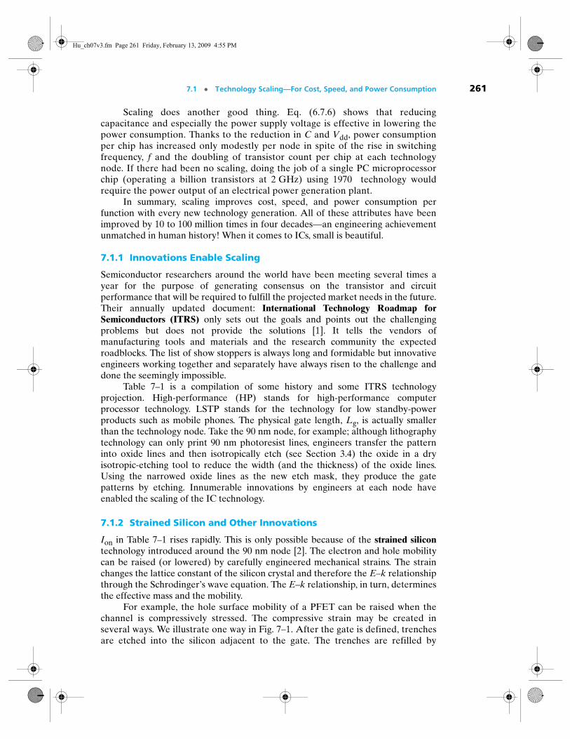
For example, the hole surface mobility of a PFET can be raised when thechannel is compressively stressed. The compressive strain may be created inseveral ways. We illustrate one way in Fig. 7–1. After the gate is defined, trenchesare etched into the silicon adjacent to the gate. The trenches are refilled by
Hu_ch07v3.fm Page 261 Friday, February 13, 2009 4:55 PM

262 Chapter 7 ● MOSFETs in ICs—Scaling, Leakage, and Other Topics
epitaxial growth (see Section 3.7.3) of SiGe—typically a 20% Ge and 80% Simixture. Because Ge atoms are larger than Si atoms and in epitaxial growth thenumber of atoms in the trench is equal to the original number of Si atoms, it is asif a large hand is forced into a small glove. A force is created that pushes on thechannel (as shown in Fig. 7–10) region and raises the hole mobility. It is alsoattractive to incorporate a thin film of Ge material in the channel itself becauseGe has higher carrier mobilities than Si [3].
In Table 7–1, EOTe or the electrical equivalent oxide thickness is the totalthickness of the gate dielectric, poly-gate depletion (if any), and the inversion layerexpressed in equivalent SiO2 thickness. It is improved (reduced) at the 45 nm nodeby a larger factor over the previous node. The enabling innovations are metal gateand high-k dielectric, which will be presented in Section 7.4.
TABLE 7–1 • Scaling from 90 nm to 22 nm and innovations that enable the scaling.
Year of Shipment 2003 2005 2007 2010 2013
Technology Node (nm) 90 65 45 32 22
Lg (nm) (HP/LSTP) 37/65 26/45 22/37 16/25 13/20
EOTe(nm) (HP/LSTP) 1.9/2.8 1.8/2.5 1.2/1.9 0.9/1.6 0.9/1.4
VDD (V) (HP/LSTP) 1.2/1.2 1.1/1.1 1.0/1.1 1.0/1.0 0.9/0.9
Ion, HP (µA/µm) 1100 1210 1500 1820 2200
Ioff , HP (µA/µm) 0.15 0.34 0.61 0.84 0.37
Ion, LSTP (µA/µm) 440 465 540 540 540
Ioff, LSTP (µA/µm) 1E-5 1E-5 3E-5 3E-5 2E-5
Innovations Strained Silicon
High-k/metal-gate
Wet lithography
New Structure
HP: High-Performance technology. LSTP: Low Standby Power technology for portable applications. EOTe: Equivalent electrical Oxide Thickness, i.e., equivalent Toxe. Ion: NFET Ion.
FIGURE 7–1 Example of strained-silicon MOSFET. Hole mobility can be raised with acompressive mechanical strain illustrated with the arrows pushing on the channel region.
Both trenchesfilled with epitaxialSiGe
Gate
N-type Si
Hu_ch07v3.fm Page 262 Friday, February 13, 2009 4:55 PM

7.2 ● Subthreshold Current—“Off” Is Not Totally “Off” 263
At the 32 nm node, wet lithography (see Section 3.3.1) is used to print the finepatterns. At the 22 nm node, new transistor structures may be used to reverse thetrend of increasing Ioff, which is the source of a serious power consumption issue.Some new structures are presented in Section 7.8.
7.2 SUBTHRESHOLD CURRENT—“OFF” IS NOT TOTALLY “OFF”
Circuit speed improves with increasing Ion; therefore, it would be desirable to use asmall Vt. Can we set Vt at an arbitrarily small value, say 10 mV? The answer is no.
At Vgs < Vt, an N-channel MOSFET is in the off state. However, a leakagecurrent can still flow between the drain and the source. The MOSFET currentobserved at Vgs < Vt is called the subthreshold current. This is the main contributorto the MOSFET off-state current, Ioff. Ioff is the Id measured at Vgs = 0 andVds = Vdd. It is important to keep Ioff very small in order to minimize the staticpower that a circuit consumes when it is in the standby mode. For example, if Ioff isa modest 100 nA per transistor, a cell-phone chip containing one hundred milliontransistors would consume 10 A even in standby. The battery would be drained inminutes without receiving or transmitting any calls. A desktop PC processor woulddissipate more power because it contains more transistors and face expensiveproblems of cooling the chip and the system.
Figure 7–2a shows a subthreshold current plot. It is plotted in a semi-log Ids vs.Vgs graph. When Vgs is below Vt, Ids is clearly a straight line, i.e., an exponentialfunction of Vgs.
Figure 7–2b–d explains the subthreshold current. At Vgs below Vt, theinversion electron concentration (ns) is small but nonetheless can allow a smallleakage current to flow between the source and the drain. In Fig. 7–2b, a larger Vgswould pull the Ec at the surface closer to EF, causing ns and Ids to rise. From theequivalent circuit in Fig. 7–2c, one can observe that
(7.2.1)
(7.2.2)
Integrating Eq. (7.2.1) yields
(7.2.3)
Ids is proportional to ns, therefore
(7.2.4)
A practical and common definition of Vt is the Vgs at which Ids = 100 nA × W/Las shown in Fig. 6–12. (Some companies may use 200 nA instead of 100 nA.).Equation (7.2.4) may be rewritten as
(7.2.5)
●● ●
dϕsdVgs------------
CoxeCoxe Cdep+------------------------------- 1
η---≡=
η 1CdepCoxe------------+=
ϕs constant Vg η⁄+=
Ids ns eqϕs kT⁄
eq constant+Vg η⁄( ) kT⁄
eqVg ηkT⁄
∝ ∝ ∝ ∝
Ids nA( ) 100 WL----- e
q Vgs Vt–( ) ηkT⁄⋅ ⋅=
Hu_ch07v3.fm Page 263 Friday, February 13, 2009 4:55 PM

264 Chapter 7 ● MOSFETs in ICs—Scaling, Leakage, and Other Topics
FIGURE 7–2 The current that flows at Vgs < Vt is called the subthreshold current. Vt ~ 0.2 V.The lower/upper curves are for Vds = 50 mV/1.2 V. After Ref. [2]. (b) When Vg is increased,Ec at the surface is pulled closer to EF, causing ns and Ids to rise; (c) equivalent capacitancenetwork; (d) subthreshold I-V with Vt and Ioff. Swing, S, is the inverse of the slope in thesubthreshold region.
Coxe
�Vg
Cdep
�s�s
��s��s
EF
Vg
Ec
EF
(b) (c)
Log (Ids )
1/S
Ioff
Vt Vgs
Vds � Vdd
100nA � W/L
mA
�A
nA
(d)
10000PMOS NMOS
(a)
1000
100
10
1
0.1
0.01
0.001�1.2 0
Vgs (V)
(Vds) � 0.05, 1.2V
I d (
�A
/�m
)
0.3 0.6 0.9 1.2�0.9 �0.6 �0.3
Hu_ch07v3.fm Page 264 Friday, February 13, 2009 4:55 PM

7.2 ● Subthreshold Current—“Off” Is Not Totally “Off” 265
Clearly, Eq. (7.2.5) agrees with the definition of Vt and Eq. (7.2.4). Thesimplicity of Eq. (7.2.5) is another reason for favoring the new Vt definition. Atroom temperature, the function exp(qVgs/kT) changes by 10 for every 60 mVchange in Vgs, therefore exp(qVgs/ηkT) changes by 10 for every η × 60 mV. Forexample, if η = 1.5, Eq. (7.2.5) states that Ids drops by ten times for every 90 mVof decrease in Vgs below Vt at room temperature. η × 60 mV is called thesubthreshold swing and represented by the symbol, S.
(7.2.6)
(7.2.7)
(7.2.8)
For given W and L, there are two ways to minimize Ioff illustrated inFig. 7–2 (d). The first is to choose a large Vt. This is not desirable because a largeVt reduces Ion and therefore degrades the circuit speed (see Eq. (6.7.1)). Thepreferable way is to reduce the subthreshold swing. S can be reduced by reducingη. That can be done by increasing Coxe (see Eq. 7.2.2), i.e., using a thinner Tox,and by decreasing Cdep, i.e., increasing Wdep.1 An additional way to reduce S, andtherefore to reduce Ioff , is to operate the transistors at significantly lower thanthe room temperature. This last approach is valid in principle but rarely usedbecause cooling adds considerable cost.
Besides the subthreshold leakage, there is another leakage currentcomponent that has becomes significant. That is the tunnel leakage through verythin gate oxide that will be presented in Section 7.4. The drain to the body junctionleakage is the third leakage component.
1 According to Eq. 6.5.2 and Eq. 7.2.2, η should be equal to m. In reality, η is larger than m becauseCoxe is smaller at low Vgs (subthreshold condition) than in inversion due to a larger Tinv as shown inFig. 5–25. Nonetheless, η and m are closely related.
S mV decade⁄( ) η 60 mV T300K--------------⋅⋅=
Ids nA( ) 100 WL----- e
q Vgs Vt–( ) ηkT⁄100 W
L----- 10
Vgs Vt–( ) S⁄⋅ ⋅=⋅ ⋅=
Ioff nA( ) 100 WL----- e
q– Vt ηkT⁄100 W
L----- 10
Vt– S⁄⋅ ⋅=⋅ ⋅=
● The Effect of Interface States ●
The subthreshold swing is degraded when interface states are present (seeSection 5.7). Figure 7–3 shows that when ϕS changes, some of the interface trapsmove from above the Fermi level to below it or vice versa. As a result, these interfacetraps change from being empty to being occupied by electrons. This change of chargein response to change of voltage (ϕS) has the effect of a capacitor. The effect of theinterface states is to add a parallel capacitor to Cdep in Fig. 7–2c. The subthresholdswing is poor unless the semiconductor-dielectric interface has low density ofinterface states such as carefully prepared Si-SiO2 interface. The subthreshold swingis often degraded after a MOSFET is electrically stressed (see sidebar in Section 5.7)and new interface states are generated.
Hu_ch07v3.fm Page 265 Friday, February 13, 2009 4:55 PM

266 Chapter 7 ● MOSFETs in ICs—Scaling, Leakage, and Other Topics
7.3 Vt ROLL-OFF—SHORT-CHANNEL MOSFETS LEAK MORE
The previous section pointed out that Vt must not be set too low; otherwise, Ioffwould be too large. The present section extends that analysis to show that thechannel length (L) must not be too short. The reason is this: Vt drops withdecreasing L as illustrated in Fig. 7–4. When Vt drops too much, Ioff becomes toolarge and that channel length is not acceptable.
FIGURE 7–3 (a) Most of the interface states are empty because they are above EF. (b) Atanother Vg, most of the interface states are filled with electrons. As a result, the interfacecharge density changes with Vg.
EF
(a)
EF
(b)
EXAMPLE 7–1 Subthreshold Leakage Current
An N-channel transistor has Vt = 0.34 V and S = 85 mV, W = 10 µm andL = 50 nm. (a) Estimate Ioff. (b) Estimate Ids at Vg = 0.17 V.
SOLUTION:
a. Use Eq. (7.2.6).
b. Use Eq. (7.2.7).
Ioff nA( ) 100 WL----- 10
Vt S⁄–⋅ ⋅ 100 10
0.05---------- 10 0.34 0.0085⁄– 2 nA=⋅ ⋅= =
Ids 100 WL----- 10
Vg Vt–( ) S⁄⋅ ⋅ 100 10
0.05---------- 10 0.17 0.34–( ) 0.085⁄ 200 nA=⋅ ⋅= =
●● ●
● Gate Length (Lg) vs. Electrical Channel Length (L) ●
Gate length is the physical length of the gate and can be accurately measured with ascanning electron microscope (SEM). It is carefully controlled in the fabricationplant. The channel length, in comparison, cannot be determined very accurately andeasily due to the lateral diffusion of the source and drain junctions. L tracks Lg butthe difference between the two just cannot be quantified precisely in spite of effortssuch as described in Section 6.11. As a result, Lg is widely used in lieu of L in datapresentations as is done in Fig. 7–4. L is still a useful concept and is used in theoreti-cal equations even though L cannot be measured precisely for small transistors.
Hu_ch07v3.fm Page 266 Friday, February 13, 2009 4:55 PM

7.3 ● Vt Roll-Off—Short-Channel MOSFETs Leak More 267
At a certain Lg, Vt becomes so low that Ioff becomes unacceptable [seeEq. (7.2.8)]. Doping the bodies of the short-channel devices more heavily than thelong-channel devices would raise their Vt. Still, at a certain Lg, Vt is so sensitive tothe manufacturing caused variation in L that the worst case Ioff becomesunacceptable. Device development engineers must design the device such that theVt roll-off does not prevent the use of the targeted minimum Lg, e.g., those listed inthe second row of Table 7–1.
Why does Vt decrease with decreasing L? Figure 7–5 illustrates a model forunderstating this effect. Figure 7–5a shows the energy band diagram along thesemiconductor–insulator interface of a long channel device at Vgs = 0. Figure 7–5bshows the case at Vgs = Vt. In the case of (b), Ec in the channel is pulled lower than
FIGURE 7–4 |Vt| decreases at very small Lg. This phenomenon is called Vt roll-off. Itdetermines the minimum acceptable Lg because Ioff is too large when Vt becomes too low ortoo sensitive to Lg.
0.01 0.1 1�0.25
�0.20
�0.15
�0.10
�0.05
0.00
Vds � 1.0 VVds � 50 mV
Vt R
oll-
off (
V)
Lg (�m)
FIGURE 7–5 a–d: Energy band diagram from source to drain when Vgs = 0 V and Vgs = Vt.a–b long channel; c–d short channel.
~0.2 V
Ec
Vds
Vgs � 0 V
Short ChannelLong Channel
Vgs � Vt-long Vgs � Vt-short
Vgs � 0 V
N� Source
N� Drain
(a) (c)
(b) (d)
Ef
Ef
Hu_ch07v3.fm Page 267 Friday, February 13, 2009 4:55 PM

268 Chapter 7 ● MOSFETs in ICs—Scaling, Leakage, and Other Topics
in case (a) and therefore is closer to the Ec in the source. When the channel Ec isonly ~0.2 eV higher than the Ec in the source (which is also ~EFn), ns in the channelreaches ~1017 cm3 and inversion threshold condition (Ids = 100nA × W/L) isreached. We may say that a 0.2 eV potential barrier is low enough to allow theelectrons in the N+ source to flow into the channel to form the inversion layer. Thefollowing analogy may be helpful for understanding the concept of the energybarrier height. The source is a reservoir of water; the potential barrier is a dam; andVgs controls the height of the dam. When Vgs is high enough, the dam is sufficientlylow for the water to flow into the channel and the drain. That defines Vt.
Figure 7–5c shows the case of a short-channel device at Vgs = 0. If the channel isshort enough, Ec will not be able to reach the same peak value as in Fig. 7–5a. As aresult, a smaller Vgs is needed in Fig. 7–5d than in Fig. 7–5b to pull the barrier down to0.2 eV. In other words, Vt is lower in the short channel device than the long channeldevice. This explains the Vt roll-off shown in Fig. 7–4.
We can understand Vt roll-off from another approach. Figure 7–6 shows acapacitor between the gate and the channel. It also shows a second capacitor, Cd,between the drain and the channel terminating at around the middle of the channel,where Ec peaks in Fig. 7–5d. As the channel length is reduced, the drain to source andthe drain to “channel” distances are reduced; therefore, Cd increases. Do not beconcerned with the exact definition or value of Cd. Instead, focus on the concept thatCd represents the capacitive coupling between the drain and the channel barrier point.
From this two-capacitor equivalent circuit, it is evident that the drain voltagehas a similar effect on the channel potential as the gate voltage. Vgs and Vds,together, determine the channel potential barrier height shown in Fig. 7–5. WhenVds is present, less Vgs is needed to pull the barrier down to 0.2 eV; therefore, Vt islower by definition. This understanding gives us a simple equation for Vt roll-off,
(7.3.1)
where Vt-long is the threshold voltage of a long-channel transistor, for which Cd = 0.More accurately, Vds should be supplemented with a constant that represents thecombined effects of the 0.2 V built-in potentials between the N– inversion layer andboth the N+ drain and source at the threshold condition [4].
(7.3.2)
Using Fig. 7–6, one can intuitively see that as L decreases, Cd increases. Recallthat the capacitance increases when the two electrodes are closer to each other.That intuition is correct for the two-dimensional geometry of Fig. 7–6, too.However, solution of the Poisson’s equation (Section 4.1.3) indicates that Cd is anexponential function of L in this two-dimensional structure [5]. Therefore,
(7.3.3)
where (7.3.4)
Xj is the drain junction depth. Equation (7.3.3) provides a semi-quantitative modelof the roll-off of Vt as a function of L and Vds. It can serve as a guide for designing
Vt Vt-long VdsCd
Coxe-----------⋅–=
Vt Vt-long Vds 0.4 V+( )Cd
Coxe-----------⋅–=
Vt Vt-long Vds 0.4 V+( ) eL ld⁄–
⋅–=
ld ToxeWdepXj3∝
Hu_ch07v3.fm Page 268 Friday, February 13, 2009 4:55 PM

7.3 ● Vt Roll-Off—Short-Channel MOSFETs Leak More 269
small MOSFET and understanding new transistor structures. At a very large L, Vtis equal to Vt-long as expected. The roll-off is an exponential function of L. The roll-off is also larger at larger Vds, which can be as large as Vdd. The acceptable Ioffdetermines the acceptable Vt through Eq. (7.2.8). This in turn determines theacceptable minimum L through Eq. (7.3.3). The acceptable minimum L is severaltimes of ld. The concept that the drain can lower the source–channel barrier andreduce Vt is called drain-induced barrier lowering or DIBL. ld may be called theDIBL characteristic length. In order to support the reduction of L at each newtechnology node, ld must be reduced in proportion to L. This means that we mustreduce Tox, Wdep, and/or Xj. In reality, all three are reduced at each node to achievethe desired reduction in ld. Reducing Tox increases the gate control or Coxe.Reducing Xj decreases Cd by reducing the size of the drain electrode. ReducingWdep also reduces Cd by introducing a ground plane (the neutral region of thesubstrate or the bottom of the depletion region) that tends to electrostaticallyshield the channel from the drain.
The basic message in Eq. (7.3.4) is that the vertical dimensions in a MOSFET(Tox, Wdep, Xj) must be reduced in order to support the reduction of the gate length.As an example, Fig. 7–7 shows that the oxide thickness has been scaled roughly inproportion to the line width (gate length).
FIGURE 7–6 Schematic two-capacitor network in MOSFET. Cd models the electrostaticcoupling between the channel and the drain. As the channel length is reduced, drain to“channel” distance is reduced; therefore, Cd increases.
FIGURE 7–7 In the past, the gate oxide thickness has been scaled roughly in proportion tothe line width.
N�
Coxe
Vgs
VdsXjCd
Wdep
Tox
P-Sub
SiO2 thickness
100
10
350
nm
250
nm
180
nm
130
nm
90 n
m
Thi
ckne
ss (
Å)
Technology node
Hu_ch07v3.fm Page 269 Friday, February 13, 2009 4:55 PM

270 Chapter 7 ● MOSFETs in ICs—Scaling, Leakage, and Other Topics
7.4 REDUCING GATE-INSULATOR ELECTRICAL THICKNESS AND TUNNELING LEAKAGE
SiO2 has been the preferred gate insulator since silicon MOSFET’s beginning. Theoxide thickness has been reduced over the years from 300 nm for the 10 µmtechnology to only 1.2 nm for the 65 nm technology. There are two reasons for therelentless drive to reduce the oxide thickness. First, a thinner oxide, i.e., a larger Coxraises Ion and a large Ion raises the circuit speed [see Eq. (6.7.1)]. The second reasonis to control Vt roll-off (and therefore the subthreshold leakage) in the presence ofa shrinking L according to Eqs. (7.3.3) and (7.3.4). One must not underestimate theimportance of the second reason. Figure 7–7 shows that the oxide thickness hasbeen scaled roughly in proportion to the line width.
Thinner oxide is desirable. What, then, prevents engineers from usingarbitrarily thin gate oxide films? Manufacturing thin oxide is not easy, but asFig. 6–5 illustrates, it is possible to grow very thin and uniform gate oxide films withhigh yield. Oxide breakdown is another limiting factor. If the oxide is too thin, theelectric field in the oxide can be so high as to cause destructive breakdown. (See thesidebar, “SiO2 Breakdown Electric Field.”) Yet another limiting factor is that long-term operation at high field, especially at elevated chip operating temperatures,breaks the weaker chemical bonds at the Si–SiO2 interface thus creating oxidecharge and Vt shift (see Section 5.7). Vt shifts cause circuit behaviors to change andraise reliability concerns.
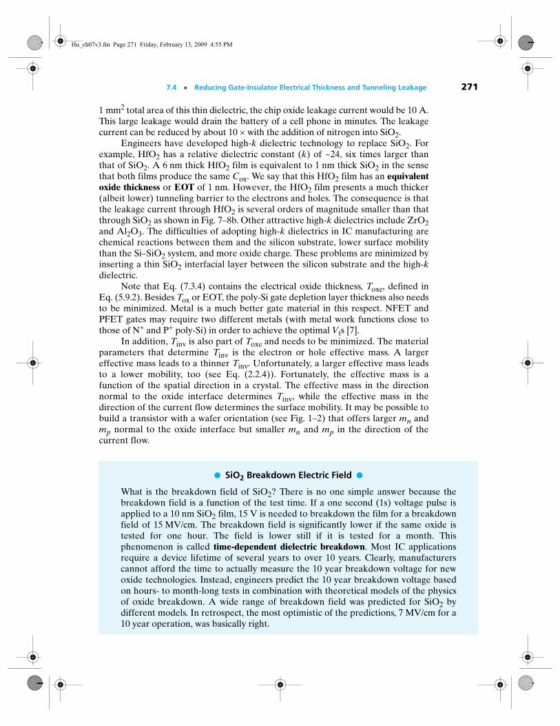
For SiO2 films thinner than 1.5 nm, tunneling leakage current becomes themost serious limiting factor. Figure 7–8a illustrates the phenomenon of gate leakageby tunneling (see Section 4.20). Electrons arrive at the gate oxide barrier at thermalvelocity and emerge on the side of the gate with a probability given by Eq. (4.20.1).This is the cause of the gate leakage current. Figure 7–8b shows that the exponentialrise of the SiO2 leakage current with decreasing thickness agrees with the tunnelingmodel prediction [6]. At 1.2 nm, SiO2 leaks 103 A/cm2. If an IC chip contains
FIGURE 7–8 (a) Energy band diagram in inversion showing electron tunneling path throughthe gate oxide; (b) 1.2 nm SiO2 conducts 103 A/cm2 of leakage current. High-k dielectric suchas HfO2 allows several orders lower leakage current to pass. (After [6]. © 2003 IEEE.)
●
●
106
0.5
Equivalent oxide thickness (nm)
Gat
e cu
rren
t den
sity
(A
/cm
2 )
1.0 1.5 2.0 2.5 3.0 3.5
104
102
100
10�2
10�4
10�6
Direct tunneling modelInversion bias| VG| � 1.0 V
Expt. DataSiO2
HfO2
(b)(a)
�
Hu_ch07v3.fm Page 270 Friday, February 13, 2009 4:55 PM
7.4 ● Reducing Gate-Insulator Electrical Thickness and Tunneling Leakage 271
1 mm2 total area of this thin dielectric, the chip oxide leakage current would be 10 A.This large leakage would drain the battery of a cell phone in minutes. The leakagecurrent can be reduced by about 10 × with the addition of nitrogen into SiO2.
Engineers have developed high-k dielectric technology to replace SiO2. Forexample, HfO2 has a relative dielectric constant (k) of ~24, six times larger thanthat of SiO2. A 6 nm thick HfO2 film is equivalent to 1 nm thick SiO2 in the sensethat both films produce the same Cox. We say that this HfO2 film has an equivalentoxide thickness or EOT of 1 nm. However, the HfO2 film presents a much thicker(albeit lower) tunneling barrier to the electrons and holes. The consequence is thatthe leakage current through HfO2 is several orders of magnitude smaller than thatthrough SiO2 as shown in Fig. 7–8b. Other attractive high-k dielectrics include ZrO2and Al2O3. The difficulties of adopting high-k dielectrics in IC manufacturing arechemical reactions between them and the silicon substrate, lower surface mobilitythan the Si–SiO2 system, and more oxide charge. These problems are minimized byinserting a thin SiO2 interfacial layer between the silicon substrate and the high-kdielectric.
Note that Eq. (7.3.4) contains the electrical oxide thickness, Toxe, defined inEq. (5.9.2). Besides Tox or EOT, the poly-Si gate depletion layer thickness also needsto be minimized. Metal is a much better gate material in this respect. NFET andPFET gates may require two different metals (with metal work functions close tothose of N+ and P+ poly-Si) in order to achieve the optimal Vts [7].
In addition, Tinv is also part of Toxe and needs to be minimized. The materialparameters that determine Tinv is the electron or hole effective mass. A largereffective mass leads to a thinner Tinv. Unfortunately, a larger effective mass leadsto a lower mobility, too (see Eq. (2.2.4)). Fortunately, the effective mass is afunction of the spatial direction in a crystal. The effective mass in the directionnormal to the oxide interface determines Tinv, while the effective mass in thedirection of the current flow determines the surface mobility. It may be possible tobuild a transistor with a wafer orientation (see Fig. 1–2) that offers larger mn andmp normal to the oxide interface but smaller mn and mp in the direction of thecurrent flow.
● SiO2 Breakdown Electric Field ●
What is the breakdown field of SiO2? There is no one simple answer because thebreakdown field is a function of the test time. If a one second (1s) voltage pulse isapplied to a 10 nm SiO2 film, 15 V is needed to breakdown the film for a breakdownfield of 15 MV/cm. The breakdown field is significantly lower if the same oxide istested for one hour. The field is lower still if it is tested for a month. Thisphenomenon is called time-dependent dielectric breakdown. Most IC applicationsrequire a device lifetime of several years to over 10 years. Clearly, manufacturerscannot afford the time to actually measure the 10 year breakdown voltage for newoxide technologies. Instead, engineers predict the 10 year breakdown voltage basedon hours- to month-long tests in combination with theoretical models of the physicsof oxide breakdown. A wide range of breakdown field was predicted for SiO2 bydifferent models. In retrospect, the most optimistic of the predictions, 7 MV/cm for a10 year operation, was basically right.
Hu_ch07v3.fm Page 271 Friday, February 13, 2009 4:55 PM

272 Chapter 7 ● MOSFETs in ICs—Scaling, Leakage, and Other Topics
7.5 HOW TO REDUCE Wdep
Equation (7.3.4) suggests that a small Wdep helps to control Vt roll-off and enablethe use of a shorter L. Wdep can be reduced by increasing the substrate doping con-centration, Nsub, because Wdep is proportional to However, Eq. (5.4.3),repeated here,
(7.5.1)
dictates that, if Vt is not to increase, Nsub must not be increased unless Cox isincreased, i.e., Tox is reduced. Equation (7.5.1) can be rewritten as Eq (7.5.2) byeliminating Nsub with Eq. (5.5.1). Clearly, Wdep can only be reduced in proportionto Tox.
(7.5.2)
This fact establishes Tox as the main enabler of L reduction according to Eq. (7.3.4).There is another way of reducing Wdep—adopt the steep retrograde doping
profile illustrated in Fig. 6–12. In that case, Wdep is determined by the thickness ofthe lightly doped surface layer. It can be shown (see sidebar) that Vt of a MOSFETwith ideal retrograde doping is
(7.5.3)
where Trg is the thickness of the lightly doped thin layer. Again, Trg in Eq. (7.5.3)can only be scaled in proportion to Tox if Vt is to be kept constant. However, Trg,the Wdep of an ideal retrograde device, can be about half the Wdep of a uniformlydoped device [see Eq. (7.5.2)] and yield the same Vt. That is an advantage of theretrograde doping. Another advantage of retrograde doping is that ionizedimpurity scattering (see Section 2.2.2) in the inversion layer is reduced and thesurface mobility can be higher. To produce a sharp retrograde profile with a verythin lightly doped layer, i.e., a very small Wdep, care must be taken to preventdopant diffusion.
This breakdown model considers a sequence of events[8]. Carrier tunnelingthrough the oxide at high field breaks up the weaker Si–O bonds in SiO2, thuscreating oxide defects. This process progresses more rapidly at those spots in theoxide sample where the densities of the weaker bonds happen to be statistically high.When the generated defects reach a critical density at any one spot, breakdownoccurs. In a longer-term stress test, the breakdown field is lower because a lower rateof defect generation is sufficient to build up the critical defect density over the longertest time. A fortuitous fact is that the breakdown field increases in very thin oxide.The charge carriers gain less energy while traversing through a very thin oxide than athick oxide film at a given electric field and are less able to create oxide defects.
● ●
1 Nsub.⁄
Vt Vfb φstqNsub2εsφst
Cox-----------------------------------+ +=
Vt Vfb φst 12εsTox
εoxWdep---------------------+
+=
Vt Vfb φst 1εsTox
εoxTrg-----------------+
+=
Hu_ch07v3.fm Page 272 Friday, February 13, 2009 4:55 PM

7.5 ● How to Reduce Wdep 273
Here is an intriguing note about reducing Wdep further. A higher Nsub inEq. (7.5.1) (and therefore a smaller Wdep) or a smaller Trg in Eq. (7.5.3) can be usedalthough it produces a large Vt than desired if this larger Vt is brought back downwith a body (or well) to source bias voltage, Vbs (see Section 6.4). The required Vbsis a forward bias across the body–source junction. A forward bias is acceptable, i.e.,the forward bias current is small, if Vbs is kept below 0.6 V.
● Derivation of Eq. (7.5.3) ●
The energy diagram at the threshold condition is shown in Fig. 7–9.
FIGURE 7–9 Energy diagram of a steep-retrograde doped MOSFET at the thresholdcondition.
The band bending, is dropped uniformly over Trg, the thickness of thelightly doped depletion layer, creating an electric field, Because of thecontinuity of the electric flux, the oxide field is Therefore,
(7.5.4)
From Eqs. (5.2.2), (7.5.4)
(7.5.5)
Trg
Ec
Ev
EF
fst
φst,�s φst Trg⁄ .=
�ox �s εs εox.⁄⋅=
Vox Tox�ox φstεsToxεoxTrg----------------= =
Vt Vfb φst 1εsTox
εoxTrg-----------------+
+=
● Predicting the Ultimate Low Limit of Channel Length—A Retrospective ●
When the channel length is too small, a MOSFET would have too large an Ioff and itceases to be a usable transistor for practical purposes. Assuming that lithography andetching technologies can produce as small features as one desires, what is theultimate low limit of MOSFET channel length?
In the 1970s, the consensus in the semiconductor industry was that the ultimatelower limit of channel length is 500 nm. In the 1980s, the consensus was 250 nm. Inthe 1990s, it was 100 nm. Now it is much smaller. What made the expertsunderestimate the channel length scaling potential?
Hu_ch07v3.fm Page 273 Friday, February 13, 2009 4:55 PM

274 Chapter 7 ● MOSFETs in ICs—Scaling, Leakage, and Other Topics
7.6 SHALLOW JUNCTION AND METAL SOURCE/DRAIN MOSFET
Figure 7–10, first introduced as Fig. 6–24b, shows the cross-sectional view of a typi-cal drain (and source) junction. Extra process steps are taken to produce the shal-low junction extension between the deep N+ junction and the channel. This shallowjunction is needed because the drain junction depth must be kept small according toEq. (7.3.4). In order to keep this junction shallow, only very short annealing at thelowest necessary temperature is used to activate the dopants and anneal out theimplantation damages in the crystal in 0.1S (flash annealing) or 1µS (laser anneal-ing) (see Section 3.6). To further reduce dopant diffusion, the doping concentrationin the shallow junction extension is kept much lower than the N+ doping density.Shallow junction and light doping combine to produce an undesirable parasiticresistance that reduces the precious Ion. That is a price to pay for suppressing Vtroll-off and the subthreshold leakage current. Farther away from the channel, asshown in Fig. 7–10, a deeper N+ junction is used to minimize total parasitic resis-tance. The width of the dielectric spacer in Fig. 7–10 should be as small as possibleto minimize the resistance.
7.6.1 MOSFET with Metal Source/Drain
A metal source/drain MOSFET or Schottky source/drain MOSFET shown inFig. 7–11a can have very shallow junctions (good for the short-channel effect) andlow series-resistance because the silicide is ten times more conductive than N+ or
A review of the historical literature reveals that the researchers weremistaken about how thin the engineers can make the gate oxide in massproduction. In the 1970s, it was thought that ~15 nm would be the limit. In the1980s, it was 8 nm, and so on. Since the Tox estimate was off, the estimates of theminimum acceptable Wdep and therefore the minimum L would be off according toEq. (7.3.4).
FIGURE 7–10 Cross-sectional view of a MOSFET drain junction. The shallow junctionextension next to the channel helps to suppress the Vt roll-off.
● ●
Silicide, e.g. NiSi2, TiSi2
Gate
Oxide
Dielectric spacerContact
N� drain
Channel
Shallow junction extension
Hu_ch07v3.fm Page 274 Friday, February 13, 2009 4:55 PM

7.6 ● Shallow Junction and Metal Source/Drain MOSFET 275
P+ Si. The only problem is that the Schottky-S/D MOSFET would have a lower Idthan the regular MOSFET if is too large to allow easy flow of carriers (electronsfor NFET) from the source into the channel.
Figure 7–11b shows the energy band diagram drawn from the source along thechannel interface to the drain. Vds is set to zero for simplicity. The energy diagram issimilar to that of a conventional MOSFET at Vg = 0 in that a potential barrier stopsthe electrons in the source from entering the channel and the transistor is off. In theon state, Fig. 7–11c, channel Ec is pulled down by the gate voltage, but not at thesource/drain edge, where the barrier height is fixed at (see Section 4.16). Thisbarrier does not exist in a conventional MOSFET as shown in Fig. 7–11d, and theycan degrade Id of the metal S/D MOSFET.
To unleash the full potentials of Schottky S/D MOSFET, a very low-Schottky junction technology should be used (for NFETs). A thin N+ region can beadded between the metal and the channel. This minimizes the effect of the barrierson current flow as shown in Fig. 4–46. Attention must be paid to reduce the largereverse leakage current of a low- Schottky drain to body junction [9].
FIGURE 7–11 (a) Metal source/drain is the ultimate way to reduce the increasinglyimportant parasitic resistance; (b) energy band diagrams in the off state; (c) in the on statethere may be energy barriers impeding current flow. These barriers do not exist in theconventional MOSFET (d) and must be minimized.
Metal
(a)
P-body
sourceMetaldrain
Gate
(b)
S D
Channel
Vg � 0
EF
Vg � Vt
Vg � Vt
Conventional MOSFET
S DChannel
EF
EF
N� N�
(c)
(d)
φB
φB
φB
φBn
Hu_ch07v3.fm Page 275 Friday, February 13, 2009 4:55 PM

276 Chapter 7 ● MOSFETs in ICs—Scaling, Leakage, and Other Topics
7.7 TRADE-OFF BETWEEN Ion AND Ioff AND DESIGN FOR MANUFACTURING
Subthreshold Ioff would not be a problem if Vt is set at a very high value. That is notacceptable because a high Vt would reduce Ion and therefore reduce circuit speed.Using a larger Vdd can raise Ion, but that is not acceptable either because it wouldraise the power consumption, which is already too large for comfort. Decreasing Lcan raise Ion but would also reduce Vt and raise Ioff.
QUESTION ● Which, if any, of the following changes lead to both sub-threshold leakage reduction and Ion enhancement? A larger Vt. A larger L. A smaller Vdd.
Figure 7–12 shows a plot of log Ioff vs. Ion of a large number of transistors [2].The trade-off between the two is clear. Higher Ion goes hand-in-hand with largerIoff. The spread in Ion (and Ioff) is due to a combination of unintentionalmanufacturing variances in Lg and Vt and intentional difference in the gate length.
Techniques have been developed to address the strong trade-off between Ionand Ioff, i.e., between speed and standby power consumption.
One technique gives circuit designers two or three (or even more) Vts tochoose from. A large circuit may be designed with only the high-Vt devices first.Circuit timing simulations are performed to identify those signal paths and circuitswhere speed must be tuned up. Intermediate-Vt devices are substituted into them.Finally, low-Vt devices are substituted into those few circuits that need even morehelp with speed. A similar strategy provides multiple Vdd. A higher Vdd is providedto a small number of circuits that need speed while a lower Vdd is used in the othercircuits. The larger Vdd provides higher speed and/or allows a larger Vt to be used(to suppress leakage). Yet the dynamic power consumption (see Eq. (6.7.6)) can bekept low because most of the circuits operate at the lower Vdd.
FIGURE 7–12 Log Ioff vs. linear Ion. The spread in Ion (and Ioff) is due to the presence ofseveral slightly different drawn Lgs and unintentional manufacturing variations in Lg and Vt.(After [2]. © 2003 IEEE.)
●
●
0.91
10
100
1000
1 1.1 1.2 1.3 1.4 1.5
Ion (mA/�m)
I off (
nA/�
m)
Hu_ch07v3.fm Page 276 Friday, February 13, 2009 4:55 PM

7.8 ● Ultra-Thin-Body SOI and Multigate MOSFETs 277
In a large circuit such as a microprocessor, only some circuit blocks need tooperate at high speed at a given time and other circuit blocks operate at lower speedor are idle. Vt can be set relatively low to produce large Ion so that circuits that needto operate at high speed can do so. A well bias voltage, Vsb in Eq. (6.4.6), is applied tothe other circuit blocks to raise the Vt and suppress the subthreshold leakage. Thistechnique requires intelligent control circuits to apply Vsb where and when needed.
This well bias technique also provides a way to compensate for the chip-to-chipand block-to-block variations in Vt that results from nonuniformity among devices dueto inevitable variations in manufacturing equipment and process. Many techniques atthe border between manufacturing and circuit design can help to ease the problem ofmanufacturing variations. These techniques are collectively known as design formanufacturing or DFM. A major cause of the device variations is the imperfect controlof Lg in the lithography process. Some of the variation is more or less random variationin nature. The other part is more or less predictable, called systematic variation. Oneexample of the systematic variations is the distortion in photolithography due to theinterference of neighboring patterns of light and darkness. Elaborate mathematicaloptical proximity correction or OPC (see Section 3.3) reshapes each pattern in thephotomask to compensate for the effect of the neighboring patterns. Another exampleis that the carrier mobility and therefore the current of a MOSFET is changed by themechanical stress effect (see Section 7.1.1) created by nearby structures, e.g., shallowtrench isolation or other MOSFETs. Sophisticated simulation tools can analyze themechanical strain and predict the Ion based on the neighboring structures and feed theIon information to circuit simulators to obtain more accurate simulation results. Anexample of random variation is the gate edge roughness or waviness caused by thegraininess of the photoresist and the poly-crystalline Si. Yet another example of randomvariation is the random dopant fluctuation phenomenon. The statistical variation of thenumber of dopant atoms and their location in small size MOSFET creates significantvariations in the threshold voltage. It requires complex design methodologies toinclude the intra-chip and inter-chip random variations in circuit design.
7.8 ULTRA-THIN-BODY SOI AND MULTIGATE MOSFETS
There are alternative MOSFET structures that are less susceptible to Vt roll-offand allow gate length scaling beyond the limit of conventional MOSFET.Figure 7–6 gives a simple description of the competition between the gate and thedrain over the control of the channel barrier height shown in Fig. 7–5. We want tomaximize the gate-to-channel capacitance and minimize the drain-to-channelcapacitance. To do the former, we reduce Tox as much as possible. To accomplishthe latter, we reduce Wdep and Xj as much as possible. It is increasingly difficult tomake these dimensions smaller. The real situation is even worse. In thesubthreshold region, Tox may be a small part Toxe in Eq. (7.3.4) because theinversion-layer thickness, Tinv in Sec. 5.9, is large. Imagine that Tox could be madeinfinitesimally small. This would give the gate a perfect control over the potentialbarrier height—but only right at the Si surface. The drain could still have morecontrol than the gate along other leakage current paths that are some distancebelow the Si surface as shown in Fig. 7–13. At this submerged location, the gate isfar away and the gate control is weak. The drain voltage can pull the potential
● ●
Hu_ch07v3.fm Page 277 Friday, February 13, 2009 4:55 PM

278 Chapter 7 ● MOSFETs in ICs—Scaling, Leakage, and Other Topics
barrier down and allow leakage current to flow along this submerged path. Thereare two transistor structures that can eliminate the leakage paths that are far awayfrom the gate [10]. One is called the ultra-thin-body MOSFET or UTB MOSFET.The other is multigate MOSFET. They are presented next.
7.8.1 Ultra-Thin-Body MOSFET and SOI
There are two ways to eliminate these submerged leakage paths. One is to use an ultra-thin-body structure as shown in Fig. 7–14 [11]. This MOSFET is built in a thin Si film onan insulator (SiO2). Since the Si film is very thin, perhaps less than 10 nm, no leakagepath is very far from the gate. (The worst-case leakage path is along the bottom of the Sifilm.) Therefore, the gate can effectively suppress the leakage. Figure 7–15 shows thatthe subthreshold leakage is reduced as the Si film is made thinner. It can be shown thatthe thin Si thickness should take the places of Wdep and Xj in Eq. (7.3.4) such that Lgcan be scaled roughly in proportion to TSi, the Si thickness. TSi should be thinner thanabout one half of the gate length in order to reap the benefit of the UTB MOSFETconcept to sustain scaling. UTB MOSFETs, as the multigate MOSFETs of the nextsection, offer additional device benefits. Because small ld (Eq. (7.3.4)) can be obtainedwithout heavy channel doping, carrier mobility is improved. The body effect that isdetrimental to circuit speed (see Section 6.4) is eliminated because the body is fullydepleted and floating and has no fixed voltage. One challenge posed by UTBMOSFETs is the large source/drain resistance due to their thinness. The solution is tothicken the source and drain with epitaxial deposition. These raised source/drains arevisible in Figs. 7–14 and 7–15.
FIGURE 7–13 The drain could still have more control than the gate along another leakagecurrent path that is some distance below the Si surface.
FIGURE 7–14 The SEM cross section of UTB device. (After [11]. © 2000 IEEE.)
Leakage path
DS
CgCd
Gate
Source DrainSiO2 Tsi � 3 nm
Hu_ch07v3.fm Page 278 Friday, February 13, 2009 4:55 PM

7.8 ● Ultra-Thin-Body SOI and Multigate MOSFETs 279
FIGURE 7–15 The subthreshold leakage is reduced as the Si film (transistor body) is madethinner. Lg = 15 nm. (After [11]. © 2000 IEEE.)
Tsi � 7 nm
Tsi � 5 nm
Tsi � 3 nm
0.0 0.2 0.4Gate voltage, Vg (V)
Dra
in c
urre
nt, I
d (A
/�m
)
0.6 0.8 1.010�11
10�10
10�9
10�8
10�7
10�6
10�5
10�4
10�3
10�2
SiO2
S DG
● SOI-Silicon on Insulator ●
Figure 7–16 shows the steps of making an SOI or silicon-on-Insulator wafer [12].(The conventional wafer is sometimes called bulk silicon wafer for clarity.) Step 1 isto implant hydrogen into a silicon wafer that has a thin SiO2 film at the surface. Thehydrogen concentration peaks at a distance D below the surface. Step 2 is to placethe first wafer, upside down, over a second plain wafer. The two wafers adhere toeach other by the atomic bonding force. A low temperature annealing causes thetwo wafers to fuse together. Step 3 is to apply another annealing step that causesthe implanted hydrogen to coalesce and form a large number of tiny hydrogenbubbles at depth D. This creates sufficient mechanical stress to break the wafer atthat plane. The final step, Step 4, is to polish the surface. Now the SOI wafer isready for use.
The Si film is of high quality and suitable for IC manufacturing. Even withoutusing an ultra-thin body, SOI provides a speed advantage because the source/drain tobody junction capacitance is practically eliminated as the source and drain diffusionregions extend vertically to the buried oxide. The cost of an SOI wafer is higher thanan ordinary Si wafer and increases the cost of IC chips. For these reasons, only somemicroprocessors, which command high prices and compete on speed, have employedthis technology so far. Figure 7–17 shows the cross-sectional SEMs of an SOIproduct. SOI also finds other compelling applications because it offers extraflexibility for making novel structures such as the ultra-thin-body MOSFET andsome multigate MOSFET structures that can be scaled to smaller gate length beyondthe capability of bulk MOSFETs.
Hu_ch07v3.fm Page 279 Friday, February 13, 2009 4:55 PM

280 Chapter 7 ● MOSFETs in ICs—Scaling, Leakage, and Other Topics
7.8.2 FinFET - Multigate MOSFET
The second way of eliminating deep submerged leakage paths is to provide gatecontrol from more than one side of the channel as shown in Fig. 7–18. The Si film is
FIGURE 7–16 Steps of making an SOI wafer. (After [12].)
FIGURE 7–17 The cross-sectional electron micrograph of an SOI integrated circuit. The lowerlevel structures are transistors and contacts. The upper two levels are the vias and theinterconnects, which employ multiple layers of materials to achieve better reliability and etch stops.
H� ions
Wafer A
A
B
B
Si bulk
New A New B
SOI wafer
or
A
A
A
Wafer B
Step 1
Step 2
Step 3
Step 4
Si
Silicon substrate
Buried Oxide
Hu_ch07v3.fm Page 280 Friday, February 13, 2009 4:55 PM

7.8 ● Ultra-Thin-Body SOI and Multigate MOSFETs 281
very thin so that no leakage path is far from one of the gates. (The worst-case pathis along the center of the Si film.) Therefore, the gate(s) can suppress leakagecurrent more effectively than the conventional MOSFET. Because there are morethan one gate, the structure may be called multigate MOSFET. The structure shownin Fig. 7–18 is a double-gate MOSFET. Shrinking TSi automatically reduces Wdepand Xj in Eq. (7.3.4) and Vt roll-off can be suppressed to allow Lg to shrink to assmall as a few nm. Because the top and bottom gates are at the same voltage andthe Si film is fully depleted, the Si surface potential moves up and down with Vg mVfor mV in the subthreshold region. The voltage divider effect illustrated in Fig. 7–1cdoes not exist and η in Eq. (7.2.4) is the desired unity and Ioff is very low. There isno need for heavy doping in the channel to reduce Wdep. This leads to low verticalfield and less impurity scattering; as a result the mobility is higher (see Section 6.3).Finally, there are two channels (top and bottom) to conduct the transistor current.For these reasons, a multigate MOSFET can have shorter Lg, lower Ioff, and largerIon than a single-gate MOSFET. But, there is one problem—how to fabricate themultigate MOSFET structure.
There is a multigate structure that is attractive for its simplicity offabrication and it is illustrated in Fig. 7–19. Consider the center structure inFig. 7–19. The process starts with an SOI wafer or a bulk Si wafer. A thin fin of Siis created by lithography and etching. Gate oxide is grown over the exposedsurfaces of the fin. Poly-Si gate material is deposited over the fin and the gate ispatterned by lithography and etching. Finally, source/drain implantation is
FIGURE 7–18 A schematic sketch of a double-gate MOSFET with gates connected.
FIGURE 7–19 Variations of FinFET. Tall FinFET has the advantage of providing a large Wand therefore large Ion while occupying a small footprint. Short FinFET has the advantage ofless challenging lithography and etching. Nanowire FET gives the gate even more control overthe transistor body by surrounding it. FinFETs can also be fabricated on bulk Si substrates.
SiSource
Gate
Gate 1
Drain
Tox
Tsi
Vg
Oxide
TallFinFET
ShortFinFET
NanowireFET
D
S
G
G G
D
SLg
D
S
Hu_ch07v3.fm Page 281 Friday, February 13, 2009 4:55 PM

282 Chapter 7 ● MOSFETs in ICs—Scaling, Leakage, and Other Topics
performed. The final structure in Fig. 7–19 is basically the multigate structure inFig.7–18 turned on its side. This structure is called the FinFET because its Si bodyresembles the back fin of a fish [13]. The channel consists of the two verticalsurfaces and the top surface of the fin. The channel width, W, is the sum of twicethe fin height and the width of the fin.
Several variations of FinFET are shown in Fig. 7–19 [14,15]. A tall FinFEThas the advantage of providing a large W and therefore large Ion while occupyinga small footprint. A short FinFET has the advantage of less challenging etching.In this case, the top surface of the fin contributes significantly to the suppressionof Vt roll-off and to leakage control. This structure is also known as a triple-gateMOSFET. The third variation gives the gate even more control over the Si wireby surrounding it. It may be called a nanowire FET and its behaviors shown inFig. 7–20 can be modeled with the same methods and concepts used to model thebasic MOSFETs. FinFETs with Lg as small as 3 nm have been experimentallydemonstrated. It will allow transistor scaling beyond the scaling limit of theconventional planar transistor.
7.9 OUTPUT CONDUCTANCE
Output conductance limits the transistor voltage gain. It has been introduced inSection 6.13. However, its cause and theory are intimately related to those of Vtroll-off. Therefore, the present chapter is a fitting place to explain it.
FIGURE 7–20 Simulated I–V curves of a nanowire MOSFET. R is the nanowire radius. (After [16].)
0.0 0.5 1.0 1.5 2.00.0
2.0 � 10�6
4.0 � 10�6
6.0 � 10�6
8.0 � 10�6
1.0 � 10�5
1.2 � 10�5
1.4 � 10�5
Dra
in c
urre
nt (
A)
Drain voltage (V)
3-D simulation model
0.0 0.5 1.0 1.5 2.01E-17
1E-15
1E-13
1E-11
1E-9
1E-7
1E-5
1E-3 R � 12.5 nmVds�1V
R � 2.5 nmTox�1.5 nmL�1 �m
Dra
in c
urre
nt (
A)
Gate voltage (V)
3-D simulationmodel
R � 2.5 nm Tox�1.5 nmL�1mm
Vgs � 2 V
Vgs � 1.5 V
Vgs � 1 V
Gate Drain
Source
● ●
Hu_ch07v3.fm Page 282 Friday, February 13, 2009 4:55 PM

7.10 ● Device and Process Simulation 283
What device design parameters determine the output conductance? Let usstart with Eq. (6.13.1),
(7.9.1)
Since Ids is a function of Vgs – Vt [see Eq. (6.9.11)], it is obvious that
(7.9.2)
The last step is the definition of gmsat given in Eq. (6.6.8). Now, Eq. (7.9.1) can beevaluated with the help of Eq. (7.3.3).
(7.9.3)
(7.9.4)
Intrinsic voltage gain was introduced in Eq. (6.13.5). Equation (7.3.3) statesthat increasing Vds would reduce Vt. That is why Ids continues to increase withoutsaturation. The output conductance is caused by the drain/channel capacitivecoupling, the same mechanism that is responsible for Vt roll-off. This is why gds islarger in a MOSFET with shorter L. To reduce gds or to increase the intrinsicvoltage gain, we can use a large L and/or reduce ld. Circuit designers routinely usemuch larger L than the minimum value allowed for a given technology node whenthe circuits require large voltage gains. Reducing ld is the job of device designersand Eq. (7.3.4) is their guide. Every design change that improves the suppression ofVt roll-off also suppresses gds and improves the voltage gain.
Vt dependence on Vds is the main cause of output conductance in very shortMOSFETs. For larger L and Vds close to Vdsat, another mechanism may be thedominant contributor to gds—channel length modulation. A voltage, Vds–Vdsat, isdissipated over a finite (non-zero) distance next to the drain. This distance increaseswith increasing Vds. As a result, the effective channel length decreases with increasingVds. Ids, which is inversely proportional to L, thus increases without true saturation.It can be shown that gds, due to the channel length modulation, is approximately
( 7.9.5)
where ld is given in Eq. (7.3.4). This component of gds can also be suppressed withlarger L and smaller Tox, Xj, and Wdep.
7.10 DEVICE AND PROCESS SIMULATION
There are commercially available computer simulation suites [17] that solve all theequations presented in this book with few or no approximations (e.g., Fermi–Diracstatistics is used rather than Boltzmann approximation). Most of these equationsare solved simultaneously, e.g., Fermi–Dirac probability, incomplete ionization ofdopants, drift and diffusion currents, current continuity equation, and Poisson
gdsdldsatdVds-------------
dldsatdVt
-------------dVtdVds------------⋅=≡
dldsatdVt
-------------d– ldsatdVgs
---------------- gmsat–= =
gds gmsat eL ld⁄–
×=
Instrinsic voltage gaingmsatgds
------------= eL ld⁄–
=
gdsld Idsat⋅
L Vds Vdsat–( )------------------------------------=
● ●
Hu_ch07v3.fm Page 283 Friday, February 13, 2009 4:55 PM
284 Chapter 7 ● MOSFETs in ICs—Scaling, Leakage, and Other Topics
equation. Device simulation is an important tool that provides the engineers withquick feedback about device behaviors. This narrows down the number of variablesthat need to be checked with expensive and time-consuming experiments.Examples of simulation results are shown in Figs. 7–15 and 7–20. Each of the figurestakes from minutes to several hours of simulation time to generate.
Related to device simulation is process simulation. The input that a userprovides to the process simulation program are the lithography mask pattern,implantation dose and energy, temperatures and times for oxide growth andannealing steps, etc. The process simulator then generates a two- or three-dimensional structure with all the deposited or grown and etched thin films anddoped regions. This output may be fed into a device simulator together with theapplied voltages and the operating temperature as the input to the devicesimulator.
7.11 MOSFET COMPACT MODEL FOR CIRCUIT SIMULATION
Circuit designers can simulate the operation of circuits containing up to hundredsof thousands or even more MOSFETs accurately, efficiently, and robustly.Accuracy must be delivered for DC as well as RF operations, analog as well digitalcircuits, memory as well as processor ICs. In circuit simulations, MOSFETs aremodeled with analytical equations much like the ones introduced in this and theprevious two chapters. More details are included in the model equations than thistextbook can introduce. These models are called compact models to highlight theircomputational efficiency in contrast with the device simulators described inSection 7.10.
It could be said that the compact model (and the layout design rules) is thelink between two halves of the semiconductor industry—technology/manufacturingon the one side and design/product on the other. A compact model must capture allthe subtle behaviors of the MOSFET over wide ranges of voltage, L, W, andtemperature and present them to the circuit designers in the form of equations.Some circuit-design methodologies, such as analog circuit design, use circuitsimulations directly. Other design methodologies use cell libraries. A cell library is acollection of hundreds of small building blocks of circuits that have been carefullydesigned and characterized beforehand using circuit simulations.
At one time, nearly every company developed its own compact models. In1997, an industry standard setting group selected BSIM [18] as the first industrystandard model. If the Ids equation of BSIM is printed out on paper, it will fill sev-eral pages.
Figure 7–21 shows selected comparisons of a compact model and measureddevice data to illustrate the accuracy of the compact model [19]. It is also importantfor the compact model to accurately model the transistor behaviors for any L andW that a circuit designer may specify. Figure 7–22 illustrates this capability. Finally,a good compact model should provide fast simulation times by using simple modelequations. In addition to the IV of N-channel and P-channel transistors, the modelalso includes capacitance models, gate dielectric leakage current model, and source
● ●
Hu_ch07v3.fm Page 284 Friday, February 13, 2009 4:55 PM

7.12 ● Chapter Summary 285
and drain junction diode model. Noise and high-frequency models are usuallyprovided, too.
7.12 CHAPTER SUMMARY
To reduce cost and improve speed in order to open up new applications, transistorsand interconnects are downsized periodically. Very small MOSFETs are prone tohave excessive leakage current called Ioff. The basic component of Ioff is thesubthreshold current
(7.2.8)
FIGURE 7–21 Selected comparisons of BSIM and measured device data to illustrate the accuracy of acompact model. (After [18].)
FIGURE 7–22 A compact model needs to accurately model the transistor behaviors for any L and W thatcircuit designers may specify. (After [19]. © 1997 IEEE.)
4.84
�4
�5
�6
�7
�8
�9
�10
�11
�12
3.87
2.90
1.94
00.0 0.8 1.6
Lines : modelSymbols : data
Lines : modelSymbols : data
2.4Vd (V)
Vgs (V) �
2.002.503.003.504.00
Vbs (V) �
0.00�0.66�1.32�1.98�2.64�3.30
I d (
mA
)
Log
Id
(A)
W/L � 10.0/0.4, T � 27oC, VB � 0 V W/L � 20.0/0.4, T � 27oC, Vd � .05 V
3.2 4.0 0.0 0.66 1.32 1.98Vg (V)
2.64 3.3
W � 20 �m Tox � 9 nmVgs � 3.292 V Tox � 9 nm
Vsub � 0 V
W � 20 �m
Vgs � 2.707 V
Vgs � 2.122 V
Vgs � 1.537 V
Vgs � 0.952 V
Vbs � �3.3 V
Vbs � �2.64 VVbs � �1.98 V
Vbs � �1.32 V
Vbs � �0.66 V
Vbs � 0 V
Vth
(V)
I dsa
t (m
A)
L (�m) L (�m)
1.6
8
6
4
2
0
1.4
1.2
1.0
0 1 2 3 4 5 6 0 1 2 3 4 5
0.8
0.6
0.4
● ●
Ioff nA( ) 100 WL----- e
q– Vt ηkT⁄100 W
L----- 10
Vt– S⁄⋅ ⋅=⋅ ⋅=
Hu_ch07v3.fm Page 285 Friday, February 13, 2009 4:55 PM

286 Chapter 7 ● MOSFETs in ICs—Scaling, Leakage, and Other Topics
S is the subthreshold swing. To keep Ioff below a given level, there is a mini-mum acceptable Vt. Unfortunately, a larger Vt is deleterious to Ion and speed.Therefore, it is important to reduce S by reducing the ratio Toxe/Wdep. Furthermore,Vt decreases with L, a fact known as Vt roll-off, caused by DIBL.
(7.3.3)
where (7.3.4)
Since Vt is a sensitive function of L, even the small (a few nm) manufacturing vari-ations in L can cause problematic variations in Vt, Ioff, and Ion. To allow L reduction,Eq. (7.3.3) states that ld must be reduced, i.e., Toxe, Wdep, and/or Xj must be reduced.
Tox reduction is limited mostly by gate tunneling leakage, which can besuppressed by replacing SiO2 with a high-k dielectric such as HfO2. Metal gate canreduce Toxe by eliminating the poly-Si gate depletion effect.
Wdep can be reduced with retrograde body doping. Xj can be reduced with mSflash annealing or the metal source–drain MOSFET structure. Xj and Wdep can alsobe reduced with the ultra-thin-body SOI device structure or the multigateMOSFET structure. More importantly, these new structures eliminate the morevulnerable leakage paths, which are the farthest from the gate.
Equation (7.3.3) also provides a theory for output conductance of the shortchannel transistors.
(7.9.3)
PROBLEMS
● Subthreshold Leakage Current ●
7.1 Assume that the gate oxide between an n+ poly-Si gate and the p-substrate is 11 Åthick and Na = 1E18 cm–3.
(a) What is the Vt of this device?
(b) What is the subthreshold swing, S?
(c) What is the maximum leakage current if W = 1 µm, L = 18 nm? (Assume Ids =100 W/L (nA) at Vg = Vt.)
● Field Oxide Leakage ●
7.2 Assume the field oxide between an n+ poly-Si wire and the p-substrate is 0.3 µm thickand that Na = 5E17 cm–3.
(a) What is the Vt of this field oxide device?
(b) What is the subthreshold swing, S?
(c) What is the maximum field leakage current if W = 10 µm, L = 0.3 µm, andVdd = 2.0 V?
● Vt Roll-off ●
7.3 Qualitatively sketch log(Ids) vs. Vg (assume Vds = Vdd) for the following:
(a) L = 0.2 µm, Na = 1E15 cm–3.
(b) L = 0.2 µm, Na = 1E17 cm–3.
Vt Vt-long Vds 0.4V+( ) eL ld⁄–
⋅–=
Id ToxeWdepXj3∝
gds gmsat eL ld⁄–
×=
● ●
Hu_ch07v3.fm Page 286 Friday, February 13, 2009 4:55 PM

Problems 287
(c) L = 1 µm, Na = 1E15 cm–3.
(d) L = 1 µm, Na = 1E17 cm–3.
Please pay attention to the positions of the curves relative to each other and label all curves.
● Trade-off between Ioff and Ion ●
7.4 Does each of the following changes increase or decrease Ioff and Ion? A larger Vt. Alarger L. A shallower junction. A smaller Vdd. A smaller Tox. Which of these changescontribute to leakage reduction without reducing the precious Ion?
7.5 There is a lot of concern that we will soon be unable to extend Moore’s Law. In yourown words, explain this concern and the difficulties of achieving high Ion and low Ioff.
(a) Answer this question in one paragraph of less than 50 words.
(b) Support your description in (a) with three hand-drawn sketches of your choice.
(c) Why is it not possible to maximize Ion and minimize Ioff by simply picking the rightvalues of Tox, Xj, and Wdep? Please explain in your own words.
(d) Provide three equations that help to quantify the issues discussed in (c).
7.6 (a) Rewrite Eq. (7.3.4) in a form that does not contain Wdep but contains Vt. Do so byusing Eqs. (5.5.1) and (5.4.3) assuming that Vt is given.
(b) Based on the answer to (a), state what actions can be taken to reduce theminimum acceptable channel length.
7.7 (a) What is the advantage of having a small Wdep?
(b) For given L and Vt, what is the impact of reducing Wdep on Idsat and gate? (Hint:consider the “m” in Chapter 6)
Discussion: Overall, smaller Wdep is desirable because it is more important to be able to suppress Vt roll-off so that L can be scaled.
● MOSFET with Ideal Retrograde Doping Profile ●
7.8 Assume an N-channel MOSFET with an N+ poly gate and a substrate with an idealizedretrograde substrate doping profile as shown in Fig. 7–23.
FIGURE 7–23
x
P�
Very light P type
OxideGate Substrate
Nsub
Tox Xrg
Hu_ch07v3.fm Page 287 Friday, February 13, 2009 4:55 PM
288 Chapter 7 ● MOSFETs in ICs—Scaling, Leakage, and Other Topics
(a) Draw the energy band diagram of the MOSFET along the x direction from thegate through the oxide and the substrate, when the gate is biased at thresholdvoltage. (Hint: Since the P region is very lightly doped you may assume that thefield in this region is constant or dε/dx = 0). Assume that the Fermi level in the P+
region coincides with Ev and the Fermi level in the N+ gate coincides with Ec.Remember to label Ec, Ev, and EF.
(b) Find an expression for Vt of this ideal retrograde device in terms of Vox. AssumeVox is known. (Hint: Use the diagram from (a) and remember that Vt is thedifference between the Fermi levels in the gate and in the substrate. At threshold,Ec of Si coincides with the Fermi level at the Si–SiO2 interface).
(c) Now write an expression for Vt in terms of Xrg, Tox, εox, εsi and any other commonparameters you see fit, but not in terms of Vox. Hint: Remember Nsub in the lightlydoped region is almost 0, so if your answer is in terms of Nsub, you might want torethink your strategy. Maybe εoxεox = εsiεsi could be a starting point.
(d) Show that the depletion layer width, Wdep in an ideal retrograde MOSFET can beabout half the Xdep of a uniformly doped device and still yield the same Vt.
(e) What is the advantage of having a small Wdep?
(f) For given L and Vt, what is the impact of reducing Wdep on Idsat and inverterdelay?
REFERENCES
1. International Technology Roadmap for Semiconductors (http://public.itrs.net/)
2. Ghani, T., et al. “A 90 Nm High Volume Manufacturing Logic Technology Featuring Novel45 nm Gate Length Strained Silicon CMOS Transistors,” IEDM Technical Digest. 2003,978–980.
3. Yeo, Y-C., et al. “Enhanced Performance in Sub-100nm CMOSFETs Using StrainedEpitaxial Si-Ge.” IEDM Technical Digest. 2000, 753–756.
4. Liu, Z. H., et al. “Threshold Voltage Model for Deep-Submicrometer MOSFETs.” IEEETrans. on Electron Devices. 40, 1 (January 1993), 86–95.
5. Wann, C. H., et al. “A Comparative Study of Advanced MOSFET Concepts.” IEEETransactions on Electron Devices. 43, 10 (October 1996), 1742–1753.
6. Yeo, Yee-Chia, et al. “MOSFET Gate Leakage Modeling and Selection Guide forAlternative Gate Dielectrics Based on Leakage Considerations.” IEEE Transactions onElectron Devices. 50, 4 (April 2003), 1027–1035.
7. Lu, Q., et al. “Dual-Metal Gate Technology for Deep-Submicron CMOS Transistor,” Symp.on VLSI Technology Digest of Technical Papers, 2000, 72–73.
8. Chen, I. C., et al. “Electrical Breakdown in Thin Gate and Tunneling Oxides.” IEEE Trans.on Electron Devices. ED-32 (February 1985), 413–422.
9. Kedzierski, J., et al. “Complementary Silicide Source/Drain Thin-Body MOSFETs for the20 nm Gate Length Regime.” IEDM Technical Digest, 2000, 57–60.
10. Hu, C. “Scaling CMOS Devices Through Alternative Structures,” Science in China(Series F). February 2001, 44 (1) 1–7.
11. Choi, Y-K., et al. “Ultrathin-body SOI MOSFET for Deep-sub-tenth Micron Era,” IEEEElectron Device Letters. 21, 5 (May 2000), 254–255.
12. Celler, George, and Michael Wolf. “Smart Cut™ A Guide to the Technology, the Process,the Products,” SOITEC. July 2003.
● ●
Hu_ch07v3.fm Page 288 Friday, February 13, 2009 4:55 PM

General References 289
13. Huang, X., et al. “Sub 50-nm FinFET: PMOS.” IEDM Technical Digest, (1999), 67–70.
14. Yang, F-L, et al. “25 nm CMOS Omega FETs.” IEDM Technical Digest. (1999), 255–258.
15. Yang, F-L, et al. “5 nm-Gate Nanowire FinFET.” VLSI Technology, 2004. Digest ofTechnical Papers, 196–197.
16. Lin, C-H., et al. “Corner Effect Model for Compact Modeling of Multi-Gate MOSFETs.”2005 SRC TECHCON.
17. Taurus Process, Synoposys TCAD Manual, Synoposys Inc., Mountain View, CA.
18. http://www-device.eecs.berkeley.edu/~bsim3/bsim4.html
19. Cheng, Y., et al. “A Physical and Scalable I-V Model in BSIM3v3 for Analog/Digital CircuitSimulation.” IEEE Trans. on Electron Devices. 44, 2, (February 1997), 277–287.
GENERAL REFERENCES
1. Taur, Y., and T. H. Ning. Fundamentals of Modern VLSI Devices. Cambridge, UK:Cambridge University Press, 1998.
2. Wolf, S. VLSI Devices. Sunset Beach, CA: Lattice Press, 1999.
● ●
Hu_ch07v3.fm Page 289 Friday, February 13, 2009 4:55 PM

Hu_ch07v3.fm Page 290 Friday, February 13, 2009 4:55 PM


![SYNCH RECTIFICATION web July2015 mm [Read-Only] · PFC PRIMARY SYNCH RECT CC/CV SUPERVISOR Primary side SMPS Secondary side. Synchronous rectification ICs • Drive power MOSFETs](https://static.fdocuments.in/doc/165x107/5f074bef7e708231d41c48d7/synch-rectification-web-july2015-mm-read-only-pfc-primary-synch-rect-cccv-supervisor.jpg)