MOSFET Small Signal Model and Analysis •Just as we did...
14
ECE 3040 - Dr. Alan Doolittle Georgia Tech MOSFET Small Signal Model and Analysis •Just as we did with the BJT, we can consider the MOSFET amplifier analysis in two parts: •Find the DC operating point •Then determine the amplifier output parameters for very small input signals.
Transcript of MOSFET Small Signal Model and Analysis •Just as we did...

ECE 3040 - Dr. Alan DoolittleGeorgia Tech
MOSFET Small Signal Model and Analysis
•Just as we did with the BJT, we can consider the MOSFET amplifier analysis in two parts:
•Find the DC operating point
•Then determine the amplifier output parameters for very small input signals.

ECE 3040 - Dr. Alan DoolittleGeorgia Tech
MOSFET Small Signal Model and Analysis
Linear Two Port Network
+V1
-
i1 i2+V2
-
I1=y11V1 + y12V2
I2=y21V1 + y22V2
General “y-parameter” Network
Non-Linear I-V relationship
(BJT, MOSFET,
etc…)
+V1
-
i1 i2+V2
-
Linearize over “small
signal range”
IGS=y11VGS + y12VDS
IDS=y21VGS + y22VDS
MOSFET “y-parameter” Network
vGS
vDS
iDS
iGS

ECE 3040 - Dr. Alan DoolittleGeorgia Tech
IGS=y11VGS + y12VDS
IDS=y21VGS + y22VDS
[ [ [IGS y11 y12 VGS
IDS y21 y22 VDS
[[[
=QVQVi
jij
DSGSV
Iy
,,,∂
∂=
Derivative of current-voltage equation evaluated at the Quiescent Point
MOSFET Small Signal Model and Analysis
( )[ ]( ) TNGSDSDSTNGSn
DS VVVforVVVK
I −≥+−= λ12
2
MOSFET Amplifiers are biased into Saturation (or Active Mode)
1.) Input Conductance
2.) Output Conductance
3.) Transconductance
00000 1211 ==⇒=∂∂
=∂∂
⇒= yandyVI
andVI
IDS
GS
GS
GSGS
( )222 2 TGS
n
DS
DS VVK
yVI
−==∂∂ λ
( )( )DSTGSnGS
DS VVVKyVI
λ+−==∂∂
121

ECE 3040 - Dr. Alan DoolittleGeorgia Tech
MOSFET Small Signal Model and AnalysisCompare with BJT Results
( )DS
DSTGS
no
V
IVV
Kgy
+=−==
λ
λ12
222
( )( )
−
=+−==
2
121TNGS
DSDSTGSnm VV
IVVVKgy λ
CEA
C
VVI
y+
=22
T
C
VI
y =21
MOSFET BJT
There is a large amount of symmetry between the MOSFET and the BJT
Each of these parameters act in the
same manner

ECE 3040 - Dr. Alan DoolittleGeorgia Tech
MOSFET Small Signal Model and AnalysisPutting the mathematical model into a small signal equivalent circuit
Compare this to the BJT small signal equivalent circuit
ECE 3040 - Dr. Alan DoolittleGeorgia Tech
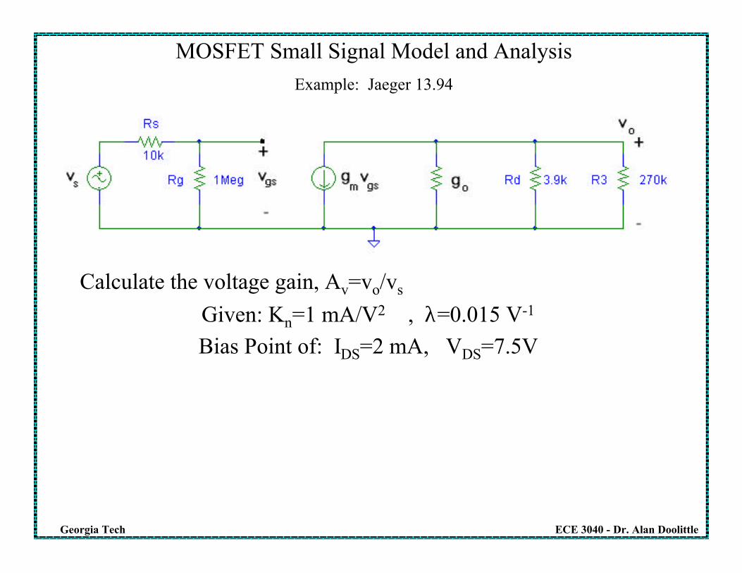
MOSFET Small Signal Model and AnalysisExample: Jaeger 13.94
Calculate the voltage gain, Av=vo/vs
Given: Kn=1 mA/V2 , λ=0.015 V-1
Bias Point of: IDS=2 mA, VDS=7.5V
ECE 3040 - Dr. Alan DoolittleGeorgia Tech
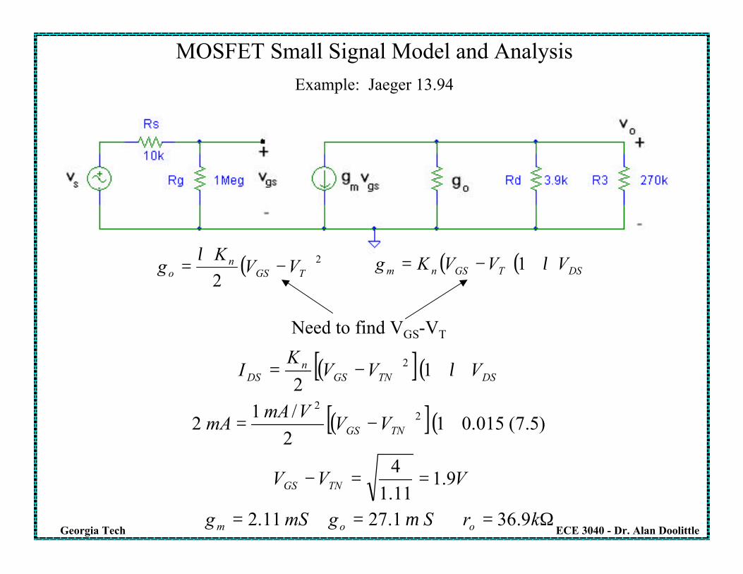
MOSFET Small Signal Model and AnalysisExample: Jaeger 13.94
( )2
2 TGSn
o VVK
g −=λ ( )( )DSTGSnm VVVKg λ+−= 1
Need to find VGS-VT
( )[ ]( )
( )[ ]( )
Ω=⇒==∴
==−
+−=
+−=
krSgmSg
VVV
VVVmA
mA
VVVK
I
oom
TNGS
TNGS
DSTNGSn
DS
9.361.2711.2
9.111.14
)5.7(015.012/1
2
12
22
2
µ
λ
ECE 3040 - Dr. Alan DoolittleGeorgia Tech
MOSFET Small Signal Model and AnalysisExample: Jaeger 13.94
( ) ( )
[ ]VVvv
vv
vv
A
kmSRRdrgvv
andMegk
Megvv
vv
vv
vv
A
GS
o
s
GS
s
ov
omGS
o
s
GS
GS
o
s
GS
s
ov
/27.7
35.748.31.2399.0110
1
−===∴
−=−=−==+
=
==
ECE 3040 - Dr. Alan DoolittleGeorgia Tech
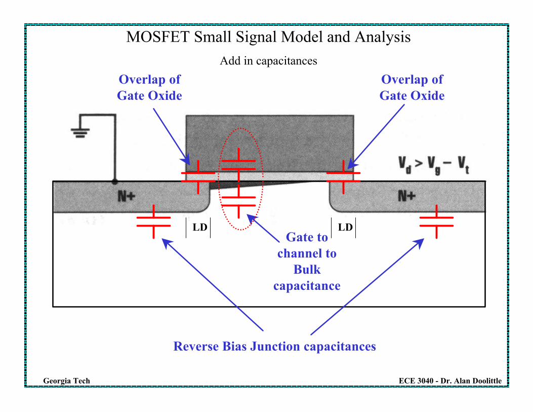
MOSFET Small Signal Model and AnalysisAdd in capacitances
Reverse Bias Junction capacitances
Overlap of Gate Oxide
Gate to channel to
Bulk capacitance
Overlap of Gate Oxide
LD LD

ECE 3040 - Dr. Alan DoolittleGeorgia Tech
MOSFET Small Signal Model and AnalysisComplete Model of a MOSFET
Reverse Bias Junction capacitances
Overlap of Gate Oxide and Gate to
channel capacitance
Overlap of Gate Oxide
Gate to channel to
Bulk capacitance
FSBmmb
Vgg
φγ
22 +=
Due to effective modulation of the threshold voltage.

ECE 3040 - Dr. Alan DoolittleGeorgia Tech
MOSFET Small Signal Model and AnalysisSPICE MOSFET Model
SPICE models the drain current ( IDS ) of an n-channel MOSFET using the following parameters/equations (SPICE variables are shown in ALLCAPPITAL LETTERS)
Cutoff: IDS = 0
Linear:
Saturation:
Threshold Voltage:
Channel LengthLEFF=L-2LD
( )[ ] ( )( )DSDSGSDSEFF
DS VLAMBDAVVTHVVLWKP
I +−−
= 12
2
( )[ ] ( )( )DSGSEFF
DS VLAMBDAVTHVLWKP
I +−
= 1
22
( )PHIVPHIGAMMAVTOV BSTH 22 −−+=

ECE 3040 - Dr. Alan DoolittleGeorgia Tech
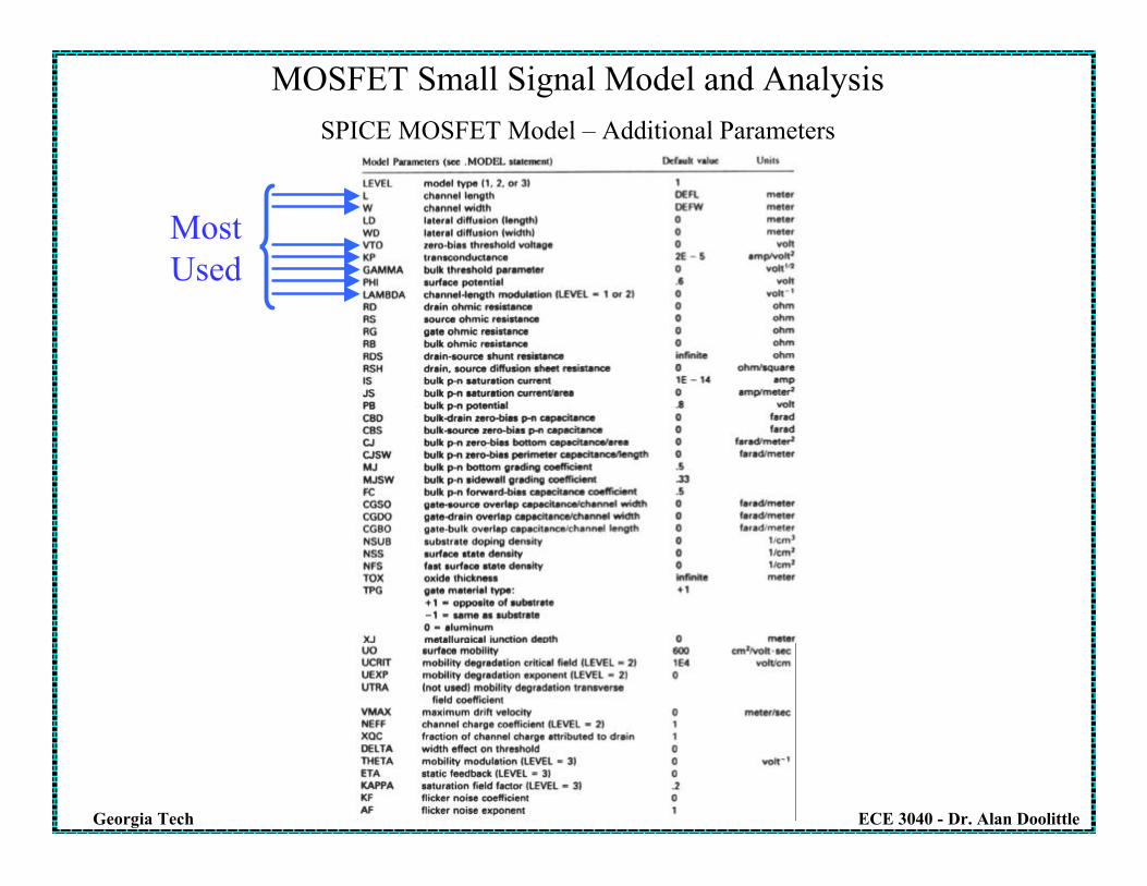
MOSFET Small Signal Model and AnalysisSPICE MOSFET Model – Additional Parameters
SPICE takes many of it’s parameters from the integrated circuit layout design:
L
W AD=WxLdiff(drain)
Ldiff(drain)Ldiff(source)
AS=WxLdiff(source)
Source Gate Drain
L = polysilicon gate length W = polysilicon gate width
AD = drain area AS = source area
PD = perimeter of drain diffusion (not including edge under gate)
PS = perimeter of source diffusion (not including edge under gate)
NRD = number of “squares” in drain diffusion
NRS = number of “squares” in source diffusion
PS=2xLdiff(source)+W PD=2xLdiff(drain)+W
Specified in terms of the minimum feature size
ECE 3040 - Dr. Alan DoolittleGeorgia Tech
MOSFET Small Signal Model and AnalysisSPICE MOSFET Model – Additional Parameters
Most Used
ECE 3040 - Dr. Alan DoolittleGeorgia Tech
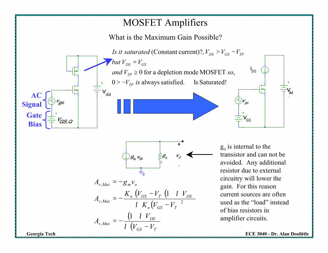
MOSFET AmplifiersWhat is the Maximum Gain Possible?
( )( )( )
( )( )TGS
DSMaxv
TGSn
DSTGSnMaxv
omMaxv
VVV
A
VVK
VVVKA
vgA
−+
−=
−+−
−=
−=
λλ
λλ
1
1
,
2,
,
Saturated! Issatisfied. always0, MOSFET modedepletion afor 0
,current)?(Constant
⇒−>≥=
−>
isVsoVand
VVbut
VVVsaturateditIs
TP
TP
GSDS
TPGSDS
go is internal to the transistor and can not be avoided. Any additional resistor due to external circuitry will lower the gain. For this reason current sources are often used as the “load” instead of bias resistors in amplifier circuits.
Gate Bias
AC Signal