MOSFET Compact Model Extensions for Circuit Simulation… · Simulation: A Perspective from...
32
MOSFET Compact Model Extensions for Circuit TRD / STD / T2D MOSFET Compact Model Extensions for Circuit Simulation: A Perspective from Industry Workshop on Next Generation MOSFET Compact Model EPFL, December 15-16, 2011 Presenter: André Juge
Transcript of MOSFET Compact Model Extensions for Circuit Simulation… · Simulation: A Perspective from...

MOSFET Compact Model Extensions for Circuit
TRD / STD / T2D
MOSFET Compact Model Extensions for Circuit Simulation: A Perspective from Industry
Workshop on Next Generation MOSFET Compact ModelEPFL, December 15-16, 2011Presenter: André Juge
Abstract
� MOSFET Compact Model Extensions for Circuit Simulation: A Perspective from Industry
� While CMOS Technology scaling has been steadily pursued to offer deca-nanometer devices, Circuit Design Community has benefited from successful development of core compact models able to capture important aspects of MOSFET electrical behavior in Circuit simulation tools. While BSIM4 models is still widely used within Industry for planar Bulk and SOI CMOS technologies, new MOSFET model generation (PSP, HiSIM…) has enabled high accuracy for design of Analog-Rf Circuits. Last, innovative modeling solutions are coming to Industry for new devices like planar FDSOI or 3D Finfet transistors.
TRD / STD / T2D
� Beyond the successful development of core device models from Academia, model extensions need to be developed in Industry for a bunch of Technology and Design dependent effects, in close interaction with the Design tool providers to enable adaptation of Design flow.
� Presentation will overview and highlight examples of modeling extensions developed in Industry to account for realistic conditions in device operation, considering device design and circuit operation; examples of applications dealing with modeling of MOSFET Parasitics, Layout Proximity effects, Process variations, and Simulation of Degradation will be presented. The presentation is intended to bring compact modelers with a survey of such effects through their potential impact, and examples of implementation.
2
Contents
� MOSFET Compact Model Extensions for Circuit Simulation: A Perspective from Industry
� Objective� Parasitic capacitances
TRD / STD / T2D
� Parasitic capacitances� Layout Proximity effects� Process variations and Statistical Variability� Reliability aware Design� Summary and Perspective
3

Objective Objective
Circuit SimulationDC/AC/TR/Noise
Vdd, Temp, Process
Core Compact Model I(V) Q(V) Noise
W/L/Nf & Temperature
LayoutParasitics
LayoutProximityEffects
ProcessVariations
AgeingHCI, NBTI,
TRD / STD / T2D4
�Core models primarily account for Bias, Geometry (W/L/NF) and Temperature dependences of devices characteristics, and need information from other tools to account for real Design, Manufacturing, and Operating conditions.
� Extended models are developed in Industry to account for MOSFET Parasitics, Layout Proximity effects, Process Variations, Statistical Variability, met by individual components after circuit integration, and Ageing effects considering device operation conditions.
�Circuit simulation methodologies need to be developped concurently with modeling effort to allow manufacturing of high yield and reliable products. Integration of Solutions in Design flow is a must.
VariationsStatisticalVariability
HCI, NBTI, PBTI,…

MOSFET Parasitic effects
� Extrinsic Parasitic capacitances
� Dependences to Layout
TRD / STD / T2D
� Modeling/Simulation approach
� Perspective and ITRS
5

MOSFET Parasitic Capacitances
Cgg + BE cap to pads
Cgg
Cgg channel +overlaps
-43%
TRD / STD / T2D6
� Even for Planar Mosfets, Parasitic Capacitances surrounding gate is a 3D problem� Cgg @Lnom almost x2 through lateral coupling between Gate and SD regions� Cgg depends on W/L, S/D cts number/pitch, distance between gate and S/D cts
+overlaps
Nmos Lnominal Gate CapacitanceMOSFET with 3D view of fully contacted SD access
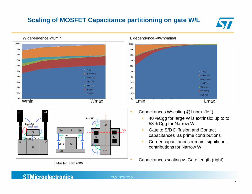
Scaling of MOSFET Capacitance partitioning on gate W/L
W dependence @Lmin L dependence @Wnominal
TRD / STD / T2D7
G
B
S
G
Cfringe
C3int
Cgate2ct
B D
cs
Ge Gc
m1
m1
SB
3Cext
Ccorner
C7
D
cs
S
Ge
Gc
AA
Cg_b
J.Mueller, SSE 2006
� Capacitances Wscaling @Lnom (left)� 40 %Cgg for large W is extrinsic; up to to
53% Cgg for Narrow W� Gate to S/D Diffusion and Contact
capacitances as prime contributions� Corner capacitances remain significant
contributions for Narrow W
� Capacitances scaling vs Gate length (right)
WmaxWmin LmaxLmin

MOSFET capacitances in real Design (S/D Contact Position vs Gate)
TRD / STD / T2D
� Capacitance dependence on SD contact position and number of contacts is significant and must be accounted in real designs
� Solutions:
� Core models or PEX tools, provided number of Mosfet instance parameters is kept minimum for large size circuit simulation
� Pre-Layout design phase: compact core model, with limited layout assumptions� Post-Layout design phase: PEX tool more adaptative to deal with variations in
Layout style.
8
Semi-regular Std cell layout (Example)Scaling Capacitances vs distance S/D Cts to Gate

MOSFET capacitances in real Design (Adaptative simulation flow)
� Pre-layout simulation (default layout) � Post-layout simulation (real layout)
circuit
contains:-network
- device instantiation - device parameters
(As/Ad/Sa/Sb/…) computed from layout
- device parameters can be
LVS stepcontains:
- network- device instantiation
TRD / STD / T2D 9
circuitnetlist
- device parameters can be “geometrical” or “electrical”
back annotatedcircuit netlist
PEX
Simulationresults
simuSimulation
results
circuitnetlist
- device instantiation- device parameters
(As/Ad/Sa/Sb/…) for default layout
- Mosfet R C parasitics for default layout , computed
by SPICE model simu
Addition of R C parasitics, computed from layout
Applies to MOSFET devices and interconnect

Verification DOEs: Impact on RO frequency
RO dgc
FEX09 Min
FEX10 X 1.43
FEX11 X 2.5
FEX12 X 5
TRD / STD / T2D10
•F increase vs dgc: benefit of extrinsic capacitance reduction•Efficient CAD accuracy monitoring methodology.
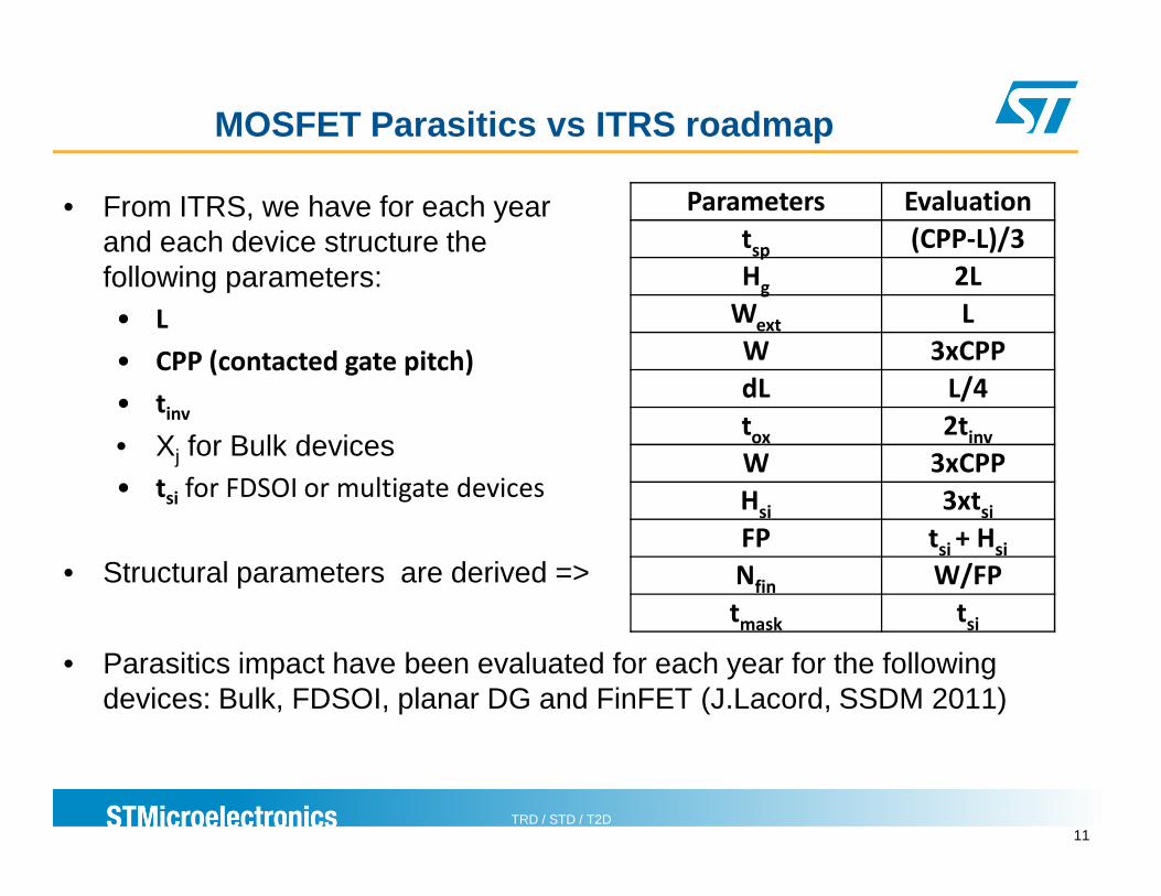
MOSFET Parasitics vs ITRS roadmap
Parameters Evaluation
tsp (CPP-L)/3
Hg 2L
Wext L
W 3xCPP
dL L/4
tox 2tinv
W 3xCPP
• From ITRS, we have for each year and each device structure the following parameters:• L
• CPP (contacted gate pitch)
• tinv
• Xj for Bulk devices
TRD / STD / T2D11
W 3xCPP
Hsi 3xtsi
FP tsi + Hsi
Nfin W/FP
tmask tsi
• Xj for Bulk devices• tsi for FDSOI or multigate devices
• Structural parameters are derived =>
• Parasitics impact have been evaluated for each year for the following devices: Bulk, FDSOI, planar DG and FinFET (J.Lacord, SSDM 2011)
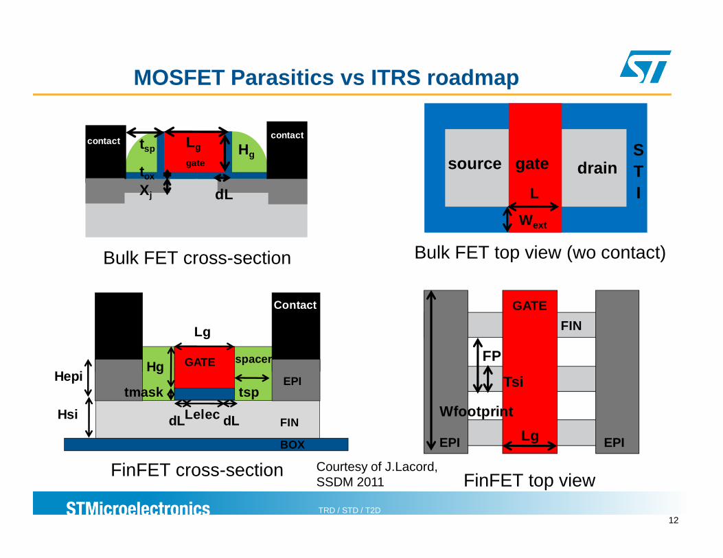
MOSFET Parasitics vs ITRS roadmap
gatesource drainSTIL
Wext
Bulk FET top view (wo contact)Bulk FET cross-section
contact
gate
contacttsp Lg
tox
Xj dL
Hg
TRD / STD / T2D
FinFET cross-section
12
Lg
tsp
Hsi
Hg
Lelec dLdL
tmaskHepi
BOX
FIN
EPI
Contact
GATE spacer
4
FIN
EPIEPI
GATE
Lg
Tsi
FP
Wfootprint
FinFET top viewCourtesy of J.Lacord, SSDM 2011
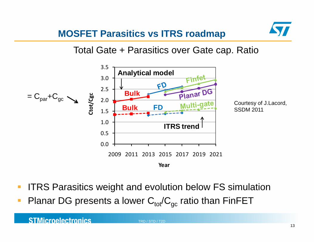
MOSFET Parasitics vs ITRS roadmap
1.0
1.5
2.0
2.5
3.0
3.5
Cto
t/C
gc Bulk
Bulk FD
Analytical model
= Cpar+Cgc
Total Gate + Parasitics over Gate cap. Ratio
Courtesy of J.Lacord, SSDM 2011
TRD / STD / T2D13
0.0
0.5
1.0
2009 2011 2013 2015 2017 2019 2021
Year
ITRS trend
� ITRS Parasitics weight and evolution below FS simulation� Planar DG presents a lower Ctot/Cgc ratio than FinFET

Layout Proximity effects
� Overview
� Modeling approach� STI example
TRD / STD / T2D
� Modeling Accuracy dilemna
� Simulation flow
� CAD Accuracy
14
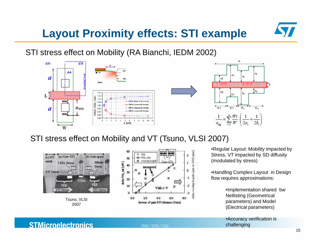
Layout Proximity effects: STI example
STI stress effect on Mobility (RA Bianchi, IEDM 2002)
TRD / STD / T2D15
Tsuno, VLSI 2007
STI stress effect on Mobility and VT (Tsuno, VLSI 2007)•Regular Layout: Mobility impacted by Stress, VT impacted by SD diffusity (modulated by stress)
•Handling Complex Layout in Design flow requires approximations:
•Implementation shared bw Netlisting (Geometrical parameters) and Model (Electrical parameters)
•Accuracy verification is challenging

MOSFET Layout Proximity effects overviewEffect Contributions Critical
distancePost-LayoutPer Instance parameters
WPE Ion scattering onwell photoresist
>1um SCA, SCB, SCC
STI(LOD) STI StressSD diffusion
1umLocal
SA, SB
STI (OD2OD) Litho and EtchSTI stress
Context1um
VT and Mu correction
Active corner rounding
Litho and Etch Local Weff correction
Gate pitch Litho and EtchCESL Stress
ContextContext up to 1 um
VT and Mu correction
WP
TRD / STD / T2D
CESL StressSD diffusion
Context up to 1 umLocal
correction
Gate cornerrounding
Litho and Etch Local Leff correction
Contacts position SD RseriesChannel stress
Local Rs and Cs correction
Others …
16
WN
• A bunch of Design dependent effects related to distances between Well, Gate, Active, Contact layer patterns and related density context•Different physical effects interplay; impact, amplitude are technology dependent•Each transistor sensitivity to each effect also depends on instance W/L

MOSFET proximity effects: Accuracy dilemna
� A bunch of effects with 1-10% impact of performance (Low Power technology), and more (High Power technology , where Stress effect is dominant)
� Characterization dilemna: Layout DOEs� WPE: 4W x 4L x 6 distances x 2 orientations x 2
N/P devices= 394 DUTs � Overall about 2K DUTs per N/P device, not
considering interaction between effects!
� CAD Netlisting dilemna : Post Layout extraction� Nb Geometrical instances > 100, loss of simulation
TRD / STD / T2D17
Layout example
� Nb Geometrical instances > 100, loss of simulation efficiency
� Pre-processing of geometrical/ electrical parameter variation through LVS: a must!
� Modeling:� Compact modeling of all effects with interactions is
not experimentally applicable� Focus on first order layout effects and their
dependence with W/L� Monitoring of CAD + Models accuracy through test
structures offering efficient test methods

MOSFET capacitances in real Design (Adaptative simulation flow)
� Pre-layout simulation (default layout) � Post-layout simulation (real layout)
circuit
contains:-network
- device instantiation - device parameters
(computed from layout-
- device parameters can be
LVS step
contains:- network
- device instantiation-
TRD / STD / T2D 18
circuitnetlist
- device parameters can be “geometrical” (Sa/Sb/Sc…)
or “electrical” (dvt, dmu)
back annotatedcircuit netlist
PEX
Simulationresults
simuSimulation
results
circuitnetlist
-- device parameters
(Sa/Sb/Sc…) for default layout
- Mosfet R C parasitics for default layout , computed by
SPICE model simu
Addition of R C parasitics, computed from layout
Applies to MOSFET devices and interconnect

MOSFET Layout Proximity effects: CAD Accuracy
PCpitch
TRD / STD / T2D
� Example of Monitoring Gate Pitch effects with Ring Oscillator: CAD to Silicon mismatch can be depicted
19
Process Variations/ Statistical Variability
� Classification
� Sources of variations
� Model requirements
TRD / STD / T2D
� Model requirements
� Impact of Global/Local Variations: RO example
� Corner vs Statistical models
20

Classification of VariationsS
yste
-m
atic
>
TRD / STD / T2D21
Sta
tis-
tical
Variations Sources at Circuit scale
Classification from D.J.Frank (IBM)
Where Compact Model Extensions can help
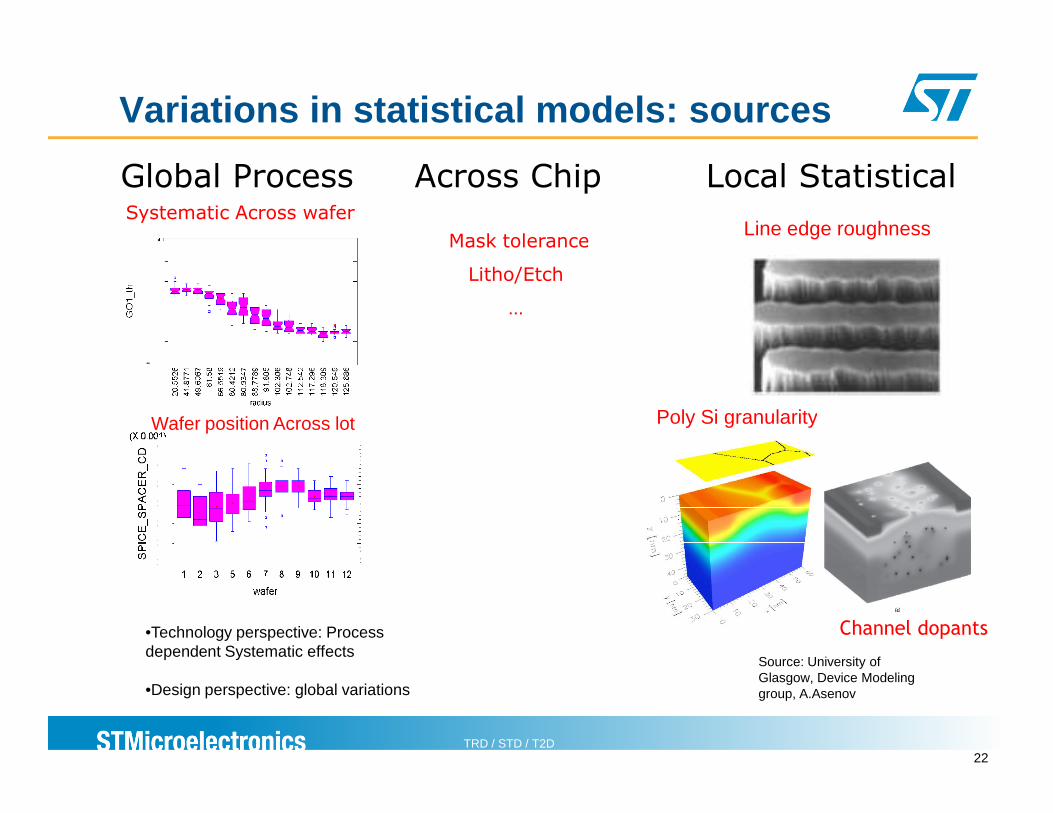
Variations in statistical models: sources
Global Process Systematic Across wafer
Local Statistical
Poly Si granularity
Line edge roughness
Across Chip
Mask tolerance
Litho/Etch
…
TRD / STD / T2D22
Wafer position Across lot
•Technology perspective: Process dependent Systematic effects
•Design perspective: global variations
Channel dopants
Poly Si granularity
Source: University of Glasgow, Device Modeling group, A.Asenov

Modeling Improvements for Local Statistical Variations (Mismatch)
� Sram SNM: � Full statistical Compact Model � Moments up to 4th order
[P.Asenov VARI 2011]
[P.Asenov VARI 2011]
TRD / STD / T2D23
Image from [Mezzomo SSE’10]
Image from [Mezzomo SSE’10]
� Analog: � SCE effect� AVT scaling on L � (pocket implants)

Impact Global/Local Variations impact: RO example
Global
Local
Global+Local
W ref: Idsat
Global
Local
Inverter: Trise
Inverter ring: Period
σ Idsat(a.u)
Trise(a.u)
Period(a.u.)
Global 1 1 1
Local 1 1 0.16
All 1.4 1.4 1.02
TRD / STD / T2D24
Global+Local
Global
Local
Global+Local
Period
�Variations impact :� Transistor: Local ~ Global� Inverter Rise time : Local ~ Global� Inverter Ring Period: Local << Global
�Circuit design needs: � Accurate compact statistical models� Accurate and Efficient simulation methods
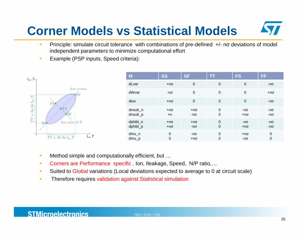
Corner Models vs Statistical Models
M SS SF TT FS FF
dLvar +nσ 0 0 0 -nσ
dWvar -nσ 0 0 0 +nσ
dtox +nσ 0 0 0 -nσ
dnsub_n dnsub_p
+nσ+n
+nσ-nσ
00
-nσ+nσ
-nσ-nσ
� Principle: simulate circuit tolerance with combinations of pre-defined +/- nσ deviations of model independent parameters to minimize computational effort
� Example (PSP inputs, Speed criteria):
TRD / STD / T2D25
� Method simple and computationally efficient, but …� Corners are Performance specific . Ion, Ileakage, Speed, N/P ratio,…� Suited to Global variations (Local deviations expected to average to 0 at circuit scale)� Therefore requires validation against Statistical simulation
dphibl_n dphibl_p
+nσ+nσ
+nσ-nσ
00
-nσ+nσ
-nσ-nσ
dmu_ndmu_p
00
-nσ+nσ
00
+nσ-nσ
00

Corner vs Statistical Models: RO example
Ion
Courtesy P.Lemoigne
TRD / STD / T2D26
� Corners ∆Ion ~ +/- 3σ, ∆tpd > +/- 3σ
tpd
Perspectives
� New devices (FDSOI planar, Finfets)
� Methodologies
� Statistical model accuracy
� Corner model methodology
TRD / STD / T2D
� Corner model methodology
� Efficient /Accurate MC simulation
27

Reliability Aware Design
� Reliability aware design
� Reliability aware modeling
� Results: Std Cells
TRD / STD / T2D
� Results: Std Cells
28
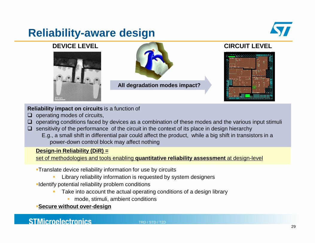
Reliability-aware design
All degradation modes impact?
DEVICE LEVEL CIRCUIT LEVEL
Reliability impact on circuits is a function of � operating modes of circuits, � operating conditions faced by devices as a combination of these modes and the various input stimuli
TRD / STD / T2D29
� operating conditions faced by devices as a combination of these modes and the various input stimuli � sensitivity of the performance of the circuit in the context of its place in design hierarchy
E.g., a small shift in differential pair could affect the product, while a big shift in transistors in a power-down control block may affect nothing
Design-in Reliability (DiR) = set of methodologies and tools enabling quantitative reliability assessment at design-level
�Translate device reliability information for use by circuits� Library reliability information is requested by system designers
�Identify potential reliability problem conditions� Take into account the actual operating conditions of a design library
� mode, stimuli, ambient conditions�Secure without over-design
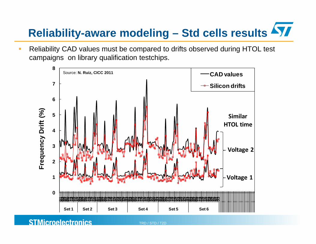
5
6
7
8
Fre
quen
cy D
rift
(%)
CAD values
Silicon drifts
Similar
HTOL time
Reliability-aware modeling – Std cells results� Reliability CAD values must be compared to drifts observed during HTOL test
campaigns on library qualification testchips.
Source: N. Ruiz, CICC 2011
TRD / STD / T2D
0
1
2
3
4
01 03 05 07 09 11 13 15 17 19 01 03 05 07 09 11 13 15 17 19 21 01 03 05 07 09 11 13 15 17 19 21 23 25 27 29 31 33 01 03 05 07 09 11 13 15 17 19 21 23 25 27 29 31 33 01 03 05 07 09 11 13 15 17 19 21 23 25 27 29 31 33 01 03 05 07 09 11 13 15 17 19 21 23 25 27 29 31 33
Set 1 Set 2 Set 3 Set 4 Set 5 Set 6
Fre
quen
cy D
rift
(%)
Voltage 1
Voltage 2
HTOL time

Summary� Mosfet parasitics are performance limiting factors
� Extrinsic cap may exceed ~x2 intrinsic cap for coming device generations
� Impact of Layout effects is difficult to estimate for coming technologies (as long as impact of each individual effect is less than 10 %) .� The experimental methodology learnings to account for these effects in current
technologies will help
TRD / STD / T2D
� Statistiscal Variability has raised from an Analog concern to a limiting factor for SRAM yield (Vddmin,…) � Both Process Variations and Statistical Variability remain concerns for modeling
new devices for Low Power / High Performance applications
� Reliability aware Design is coming: requires a set of methodologies and tools enabling quantitative life-time assessment at circuit-level
� In Industry, those subjects will keep attention from the Modeling and Reliability expert communities from now and through the coming years.
31
Acknowledgements� Prof A.Asenov and Device Modeling Group (University of Glasgow)
� for highlights on Variability modeling and simulation
� Dr Gerard Ghibaudo (IMEP)� for highlights on Variability characterization and modeling
� EU ENIAC Modern project
TRD / STD / T2D
� EU ENIAC Modern project � for supporting development of solutions for Statistical Variability
and Reliability
� ST team : � David Hoguet, Jean-Claude Marin, Vincent Quenette, Joris
Lacord, Vincent Huard, N. Ruiz, E. Pion, F.Cacho, Clément Charbuillet, P.Lemoigne
32