Monolithic buck converter for DDR memory termination€¦ · This is information on a product in...
28
This is information on a product in full production. November 2015 DocID027688 Rev 3 1/28 PM8908 Monolithic buck converter for DDR memory termination Datasheet - production data Features Integrated MOSFETs for high efficiency Current COT architecture 1 V to 3.5 V input voltage (V IN ) 5.0 V supply voltage (V CC ) Constant frequency mode 1% output voltage accuracy Two programmable switching frequencies (0.6 MHz or 1 MHz) ADJ output voltage from 0.5 V to 2 V Embedded bootstrap diode OV/UV/OC and overtemperature protection Soft-off with integrated discharge resistor External tracking Power Good output QFN20 3.5 x 4.0 mm compact package Applications Memory termination regulator for DDR3, DDR4 and low power DDR3/DDR4 Notebook/desktop/server Low voltage application for 1 V to 3.5 V input rails Description The PM8908 is a high efficiency monolithic step- down switching regulator designed mainly for the DDR termination. The IC operates from 1 V to 3.5 V input voltage (V IN ). The device uses a COT control loop that provides very good performances in terms of load and line transients. The current sense is internally thermally compensated for optimum precision. The output voltage is adjusted from 0.5 V to 2 V with ± 1% accuracy overtemperature variations. The PM8908 also provides external tracking support. The PM8908 provides positive and negative overcurrent protection as well as over/undervoltage and overtemperature protection. PGOOD output easily provides real- time information on the output voltage. The PM8908 is available in a QFN20 3.5 x 4.0 mm package. QFN20 3.5 x 4.0 mm Table 1. Device summary Order code Package Packaging PM8908TR QFN20 (3.5 x 4.0 mm) Tape and reel www.st.com
Transcript of Monolithic buck converter for DDR memory termination€¦ · This is information on a product in...

This is information on a product in full production.
November 2015 DocID027688 Rev 3 1/28
PM8908
Monolithic buck converter for DDR memory termination
Datasheet - production data
Features
Integrated MOSFETs for high efficiency
Current COT architecture
1 V to 3.5 V input voltage (VIN)
5.0 V supply voltage (VCC)
Constant frequency mode
1% output voltage accuracy
Two programmable switching frequencies (0.6 MHz or 1 MHz)
ADJ output voltage from 0.5 V to 2 V
Embedded bootstrap diode
OV/UV/OC and overtemperature protection
Soft-off with integrated discharge resistor
External tracking
Power Good output
QFN20 3.5 x 4.0 mm compact package
Applications
Memory termination regulator for DDR3, DDR4 and low power DDR3/DDR4
Notebook/desktop/server
Low voltage application for 1 V to 3.5 V input rails
Description
The PM8908 is a high efficiency monolithic step-down switching regulator designed mainly for the DDR termination.
The IC operates from 1 V to 3.5 V input voltage (VIN).
The device uses a COT control loop that provides very good performances in terms of load and line transients. The current sense is internally thermally compensated for optimum precision.
The output voltage is adjusted from 0.5 V to 2 V with ± 1% accuracy overtemperature variations.
The PM8908 also provides external tracking support.
The PM8908 provides positive and negative overcurrent protection as well as over/undervoltage and overtemperature protection. PGOOD output easily provides real-time information on the output voltage.
The PM8908 is available in a QFN20 3.5 x 4.0 mm package.
QFN20 3.5 x 4.0 mm
Table 1. Device summary
Order code Package Packaging
PM8908TR QFN20 (3.5 x 4.0 mm) Tape and reel
www.st.com

Contents PM8908
2/28 DocID027688 Rev 3
Contents
1 Typical application circuit and block diagram . . . . . . . . . . . . . . . . . . . . 4
1.1 Application circuit . . . . . . . . . . . . . . . . . . . . . . . . . . . . . . . . . . . . . . . . . . . . 4
1.2 Block diagram . . . . . . . . . . . . . . . . . . . . . . . . . . . . . . . . . . . . . . . . . . . . . . . 5
2 Pin description and connection diagrams . . . . . . . . . . . . . . . . . . . . . . . 6
Pin description . . . . . . . . . . . . . . . . . . . . . . . . . . . . . . . . . . . . . . . . . . . . . . . . . . . . 6
3 Thermal data . . . . . . . . . . . . . . . . . . . . . . . . . . . . . . . . . . . . . . . . . . . . . . . 8
4 Electrical specifications . . . . . . . . . . . . . . . . . . . . . . . . . . . . . . . . . . . . . . 9
4.1 Absolute maximum ratings . . . . . . . . . . . . . . . . . . . . . . . . . . . . . . . . . . . . . 9
4.2 Electrical characteristics . . . . . . . . . . . . . . . . . . . . . . . . . . . . . . . . . . . . . . 10
5 Device description . . . . . . . . . . . . . . . . . . . . . . . . . . . . . . . . . . . . . . . . . 13
5.1 Power section . . . . . . . . . . . . . . . . . . . . . . . . . . . . . . . . . . . . . . . . . . . . . . 13
5.2 Device configuration . . . . . . . . . . . . . . . . . . . . . . . . . . . . . . . . . . . . . . . . . 14
5.3 Startup and shutdown management . . . . . . . . . . . . . . . . . . . . . . . . . . . . . 14
Soft-off . . . . . . . . . . . . . . . . . . . . . . . . . . . . . . . . . . . . . . . . . . . . . . . . . . . . . . . . . . 16
5.4 Output voltage monitoring and protection . . . . . . . . . . . . . . . . . . . . . . . . 16
5.4.1 Overvoltage protection . . . . . . . . . . . . . . . . . . . . . . . . . . . . . . . . . . . . . . 16
5.4.2 Undervoltage protection . . . . . . . . . . . . . . . . . . . . . . . . . . . . . . . . . . . . . 17
5.4.3 Power Good (PGOOD) . . . . . . . . . . . . . . . . . . . . . . . . . . . . . . . . . . . . . 17
5.4.4 Overcurrent protection . . . . . . . . . . . . . . . . . . . . . . . . . . . . . . . . . . . . . . 17
5.4.5 Overtemperature protection . . . . . . . . . . . . . . . . . . . . . . . . . . . . . . . . . . 18
6 Application information . . . . . . . . . . . . . . . . . . . . . . . . . . . . . . . . . . . . . 19
6.1 Output voltage setting . . . . . . . . . . . . . . . . . . . . . . . . . . . . . . . . . . . . . . . 19
6.2 Droop setting . . . . . . . . . . . . . . . . . . . . . . . . . . . . . . . . . . . . . . . . . . . . . . 19
6.3 Non-droop setting . . . . . . . . . . . . . . . . . . . . . . . . . . . . . . . . . . . . . . . . . . . 20
6.4 Inductor design . . . . . . . . . . . . . . . . . . . . . . . . . . . . . . . . . . . . . . . . . . . . . 20
6.5 Output capacitors . . . . . . . . . . . . . . . . . . . . . . . . . . . . . . . . . . . . . . . . . . . 21
6.6 Input capacitors . . . . . . . . . . . . . . . . . . . . . . . . . . . . . . . . . . . . . . . . . . . . 21
6.7 Compensation network . . . . . . . . . . . . . . . . . . . . . . . . . . . . . . . . . . . . . . . 22

DocID027688 Rev 3 3/28
PM8908 Contents
28
7 Package information . . . . . . . . . . . . . . . . . . . . . . . . . . . . . . . . . . . . . . . . 23
7.1 QFN20 package information . . . . . . . . . . . . . . . . . . . . . . . . . . . . . . . . . . 24
8 Revision history . . . . . . . . . . . . . . . . . . . . . . . . . . . . . . . . . . . . . . . . . . . 27

Typical application circuit and block diagram PM8908
4/28 DocID027688 Rev 3
1 Typical application circuit and block diagram
1.1 Application circuit
Figure 1. Typical application circuit
Figure 2. Typical memory termination application circuit
L
RPGOOD
PM8908
PGOOD
EN
MODE
VOUTCOMP
REFIN
PGND
PHASE
BOOT
VINVCC
GND
VIN = 1 V to 3.5 VVCC = 5 V
CBOOT
CF
COUT
CVINCVCC
20 4, 5
1, 2, 3
11, 12, 13, 14, 15
16
10
8
9
6
19
17
18
R1
RF
RM
REF7
R2
CREF
VOUT
CP
L
RPGOOD
PM8908
PGOOD
EN
MODE
VOUTCOMP
REFIN
PGND
PHASE
BOOT
VINVCC
GND
VDDQ = 1.2 V VCC = 5 V
CBOOT
CF
COUT
CVINCVCC
20 4, 5
1, 2, 3
11, 12, 13, 14, 15
16
10
8
9
6
19
17
18
R1
RF
RM
REF7
R2
CREF
VOUT = 0.6 V
VDDQ
R1=R2
CP

DocID027688 Rev 3 5/28
PM8908 Typical application circuit and block diagram
28
1.2 Block diagram
Figure 3. Block diagram
COT CONTROL LOGIC,
PROTECTIONS&
ADAPTIVEDEAD TIMES VCC
VCC UVLO
DEAD TIMES
Discharge
THERMAL MONITOR
PM8908
PGOOD
EN
REF
VOUT
COMP
REFIN
PGND
PHASE
BOOT
VIN
GND
SS
PHASE
VCCMODE
Voltage Reference
DelayVOUT
Hy
Hy
REFIN -16%
REFIN +16%
CLCurrent
Limit
K
OV
UV
REFIN -30%
REFIN +20%
VOUT
PGND
Pin description and connection diagrams PM8908
6/28 DocID027688 Rev 3
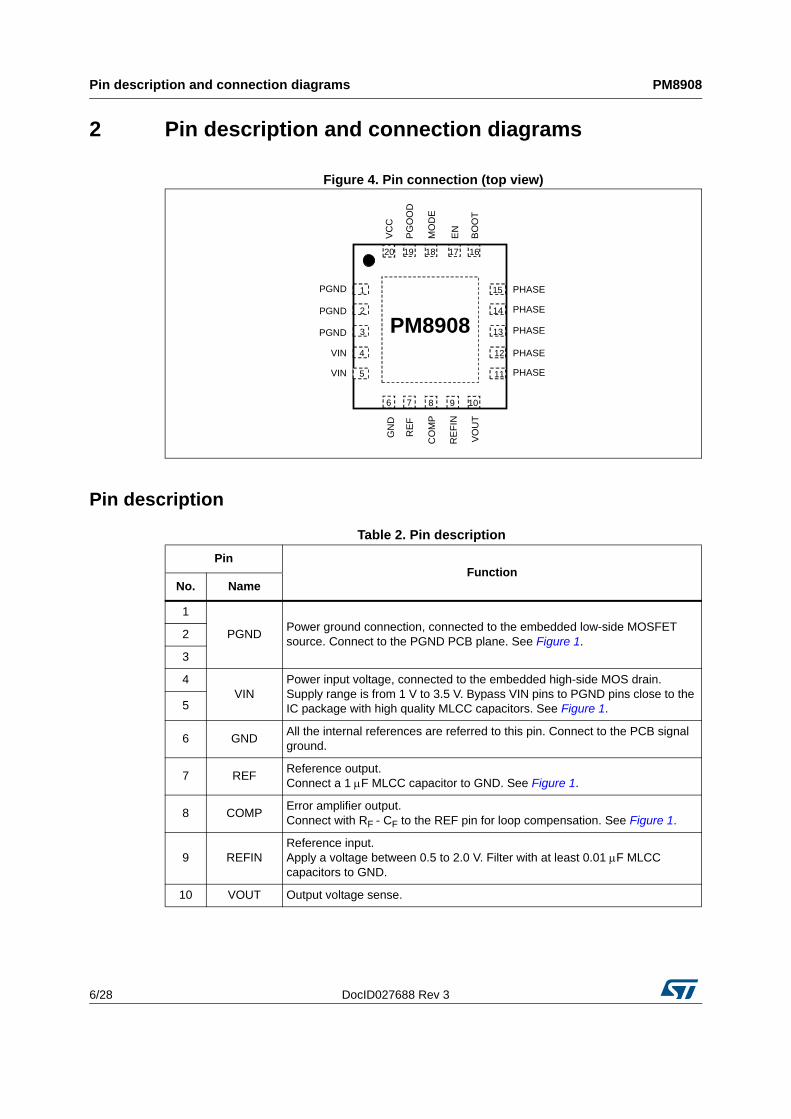
2 Pin description and connection diagrams
Figure 4. Pin connection (top view)
Pin description
1
2
3
4
PM8908PGND
VIN
PHASE
12
15
14
13
1819 1617
BO
OT
EN
MO
DE
PG
OO
D
CO
MP
1098
RE
FIN
VO
UT
RE
F7
5 11
6
20
PGND
PGND
VIN
VC
CG
ND
PHASE
PHASE
PHASE
PHASE
Table 2. Pin description
PinFunction
No. Name
1
PGNDPower ground connection, connected to the embedded low-side MOSFET source. Connect to the PGND PCB plane. See Figure 1.
2
3
4VIN
Power input voltage, connected to the embedded high-side MOS drain.Supply range is from 1 V to 3.5 V. Bypass VIN pins to PGND pins close to the IC package with high quality MLCC capacitors. See Figure 1.5
6 GNDAll the internal references are referred to this pin. Connect to the PCB signal ground.
7 REFReference output. Connect a 1 F MLCC capacitor to GND. See Figure 1.
8 COMPError amplifier output.Connect with RF - CF to the REF pin for loop compensation. See Figure 1.
9 REFINReference input.Apply a voltage between 0.5 to 2.0 V. Filter with at least 0.01 F MLCC capacitors to GND.
10 VOUT Output voltage sense.

DocID027688 Rev 3 7/28
PM8908 Pin description and connection diagrams
28
11
PHASEOutput inductor connection. The pins are connected to the embedded MOSFETs (high-side source and low-side drain). Connect directly to the output inductor. See Figure 1.
12
13
14
15
16 BOOTBootstrap pin.It provides power supply for the floating high-side MOS driver.Connect with 0.1 µF to PHASE. See Figure 1.
17 EN Enable.
18 MODESwitching frequency and the OCL programming pin. See Table 6 on page 14.
This pin must not be left floating.
19 PGOOD
Power Good pin.Open drain output set free after SS has finished and pulled low when VOUT is out of the PGOOD window or any protection is triggered. Pull up to VCC, if not used it can be left floating.
20 VCCDevice power supply.Operative voltage is 5.0 V. Filter with at least 1µF MLCC vs. GND.
Thermal padThe thermal pad of the device. Connect to the PCB ground plane with multiple VIAS.
Table 2. Pin description (continued)
PinFunction
No. Name

Thermal data PM8908
8/28 DocID027688 Rev 3
3 Thermal data
Table 3. Thermal data
Symbol Parameter Value Unit
RthJAThermal resistance junction to ambient
(Device soldered on demonstration board)40 °C/W
TMAX Maximum junction temperature 150 °C
TSTG Storage temperature range -55 to 150 °C
TJ Junction temperature range -40 to 150 °C

DocID027688 Rev 3 9/28
PM8908 Electrical specifications
28
4 Electrical specifications
4.1 Absolute maximum ratings
Note: Absolute maximum ratings are those values beyond which damage to the device may occur. These are stress ratings only and functional operation of the device at these conditions is not implied. Exposure to absolute maximum rated conditions for extended periods may affect device reliability. All voltage values are with respect to the network ground terminal.
Table 4. Absolute maximum ratings
Symbol Parameter Value(1)
1. All voltages need to be lower than VCC under any condition.
Unit
VCC To PGND, GND -0.3 to 7 V
VIN To PGND, GND -0.3 to 4 V
BOOT
To PGND, GND -0.3 to 11 V
To PGND, GND, t < 10 ns -0.3 to 12.2(2)
2. Regardless of application configuration, it is mandatory not to exceed the AMR voltage value on the BOOT and PHASE pins.
V
To PHASE -0.3 to 7 V
PHASETo PGND, GND -2 to 4 V
To PGND, GND, t < 10 ns -2.2 to 7.5(2) V
PGOOD To PGND, GND -0.3 to 7 V
EN To PGND, GND -0.3 to 7 V
VOUT To PGND, GND -1.0 to 3.6 V
REFIN, COMP, REF, MODE To GND -0.3 to 3.6 V

Electrical specifications PM8908
10/28 DocID027688 Rev 3
4.2 Electrical characteristics
VCC = 5.0 V ± 5%, TA = 25 °C (unless otherwise specified).
Table 5. Electrical characteristics
Symbol Parameter Test conditions Min. Typ. Max. Unit
Supply current and undervoltage lockout
IIN VIN shutdown current Shutdown, EN = 0 V 0.3 5 A
ICC VCC supply currentEN = H, VBOOT = 4.5 V, VCC = 4.5 V, VIN = 3.5V, VM = GND
2 3.6 mA
ICCSD VCC shutdown current Shutdown, EN = 0 V 4 10 A
IBSS Boot input currentVBOOT = 9 V, VPHASE = 3.5 V,
VCC = 5.5 V150 A
VCC VCC supply voltage 4.5 5.0 5.5 V
VCC UVLOVCC turn-on VCC rising 4.2 4.37 4.5 V
Hysteresis 440 mV
REF UVLOVREF turn-on REF rising 1.8 V
Hysteresis 100 mV
Oscillator, off-time and on-time
fSW Oscillator accuracyRM = 100 k 1
MHzRM = 47 k 0.6
tOFF-min Minimum off-timeVIN = 1.5 V, VOUT = 0.9 V, VREFIN = 1 V, fSW = 1 MHz / 0.6 MHz
170 ns
Reference and GM amplifier
VOUT Output voltage accuracy VREFIN = 1 V, no droop -1 +1 %
VREF Voltage reference IREF = 0 1.95 2.0 2.05 V
GM Transconductance(1) 1.00 mS
ICSKCOMP pin maximum sinking current
VCOMP = 2 V, VREFIN - VOUT = -80 mV 80 A
ICSRCOMP pin maximum sourcing current
VCOMP = 2 V, VREFIN - VOUT = 80 mV -80 A
VCMCommon mode input voltage range(1) 0 2 V
VDMDifferential mode input voltage range(1) 0 80 mV
VOSet Input offset 0 mV
F-3dB -3 dB frequency(1) 4.5 6.0 7.5 MHz
ACS Current sense gainGain from the current of the LS to PWM comp when PWM = OFF
47 53 59 mV/A

DocID027688 Rev 3 11/28
PM8908 Electrical specifications
28
Soft-end
RDS Phase discharge resistance 47
Overcurrent protection
IOCL Positive overcurrent threshold LS sourcing, RM = 47 k 4 7.6 11 A
IOCLN Negative overcurrent threshold LS sourcing, RM = 47 k -11 - 7.6 - 4 A
Bootstrap switch
RBSS Boot switch on-resistance IBOOT = 10 mA, TA = 25 °C 12
Over and undervoltage protection
OVP OVP threshold VOUT rising 117 120 123%
VREFIN
tOVPd OVP delayTime from the VOUT pinout of + 20% of REFIN to OVP fault
10 s
UVP UVP threshold VOUT falling 65 68 71%
VREFIN
tUVPd UVP delayTime from the VOUT pinout of -30% of REFIN to UVP fault
256 s
Undervoltage fault enable delay
Time from EN = H to undervoltage ready 2.4 ms
External tracking
Time from EN = H to undervoltage ready9 ms
Overtemperature protection
OTP
Thermal shutdown threshold(1) 145 °C
Thermal shutdown hysteresis(1) 10 °C
PGOOD
PGOOD
Upper thresholdVOUT rising 116
% VREFIN
Hysteresis 8
Lower thresholdVOUT falling 84
Hysteresis 8
VPGOOD,LPGOOD voltage low impedance
IPGOOD_SINK = 4 mA, VCC = 4.5 V 0.3 V
IPGOOD,HPGOOD leakage high impedance
VPGOOD = 5.5 V 1 A
tPGd PGOOD startup delay timeExternal tracking
Time from EN = H to PGOOD high10 ms
tPGHd PGOOD high delay time Rising edge 0.8 1 1.2 ms
tPGLd PGOOD low delay time Falling edge(2) 10 s
Table 5. Electrical characteristics (continued)
Symbol Parameter Test conditions Min. Typ. Max. Unit

Electrical specifications PM8908
12/28 DocID027688 Rev 3
ENABLE
ENInput logic high EN rising 2 V
Input logic low EN falling 0.5 V
IEN EN input current VEN = 5 V 3 A
MODE
IM Mode current VMODE from GND to 2.4 V 15 A
SOFT-START
tSS Soft-start time From EN = H to VOUT 2.4 ms
td Delay soft-start time From EN = H to VOUT ramp starts 750 s
1. Guaranteed by design, not subject to test.
2. Delay time not valid if the UVLO or EN shutdown events are occurring.
Table 5. Electrical characteristics (continued)
Symbol Parameter Test conditions Min. Typ. Max. Unit

DocID027688 Rev 3 13/28
PM8908 Device description
28
5 Device description
The PM8908 is a high efficiency synchronous step-down monolithic switching regulator capable to deliver or sink the current.
The power input voltage (VIN) can range from 1 V to 3.5 V, the signal input voltage (VCC) can range from 4.5 V to 5.5 V.
The output voltage is regulated to the REFIN voltage which comes from an external reference voltage. The output voltage accuracy is better than ±1% over the line, load and temperature.
The PM8908 embeds low RDS(on) N-channel MOSFETs for both HS (high-side) and LS (low-side).
The high-switching frequency selectable in two values - 600 kHz or 1 MHz and the small package allows very compact VR solutions.
In the COT the tON is function of VIN, VOUT and switching frequency (fSW), as shown in Equation 1:
Equation 1
The PM8908 features a full set of protections and output voltage monitoring:
Precise and accurate overcurrent limit (internally compensated against temperature variations)
Over and undervoltage protection
Overtemperature protection
Undervoltage lockout on analog supply (VCC)
Power Good open drain output easily provides real-time information about the output voltage.
The dedicated ENABLE pin (EN) offers easy control on the power sequencing. Forcing the EN low, the device enters the shutdown state and absorbs a total quiescent current from VCC and VIN less than 15 µA.
5.1 Power section
The PM8908 integrates two low RDS(on) N-channel MOSFETs as low-side and high-side switches, optimized for fast switching transition and high efficiency over the entire load range.
The HS MOSFET drain is connected to the VIN pins (power input), the LS MOSFET source is connected to the PGND pins (power ground), and the HS MOSFET source and LS MOSFET drain are connected together and to the PHASE pins (see Figure 1 on page 4). The driving section is supplied from the VCC pins that assure the proper driving voltage over all the VIN range.
tON
VOUT
VIN fSW-----------------------=

Device description PM8908
14/28 DocID027688 Rev 3
To properly supply the power section is advised following:
Bypass VIN pins to PGND pins as close as possible to the IC package with high quality MLCC capacitors.
Connect the bootstrap capacitor (typically a 100 nF ceramic capacitor rated to stand VIN voltage) from the BOOT pin to the PHASE pin to supply the HS driver.
Caution: Do not connect an external bootstrap diode. The IC already integrates an active bootstrap switch to charge the bootstrap capacitor, saving the cost of this external component.
The PM8908 embodies the anti shoot-through and adaptive deadtime control to minimize low-side body diode conduction time and consequently to reduce power losses:
When the gate driving voltage of the HS drops (to check high-side MOSFET turn-off), the LS MOSFET is suddenly switched on
When the gate driving voltage of the LS drops (to check low-side MOSFET turn-off), the HS MOSFET is suddenly switched on.
5.2 Device configuration
The PM8908 has a programming pin - MODE (pin 18) - which allows choosing the regulator switching frequency and the OCL threshold. This programming feature is performed by selecting the proper resistor, to be mounted between the pin 18 to ground, as summarized in Table 6.
Note: The MODE pin must not be left floating.
5.3 Startup and shutdown management
The IC monitors the supply voltage on the VCC pin. Once VCC voltage is above the UVLO (undervoltage lockout) threshold and the EN pin is above the turn-on threshold:
If the IC is configured for tracking application (see Figure 2 on page 4), the output voltage is regulated to the REFIN voltage. In order to discriminate between the non-tracking and the tracking, there is a delay time of 750 s required between the EN or the VCC UVLO threshold and REFIN voltage. REFIN voltage must be applied within 9 ms (typ.) from the EN high (see Figure 5).
If the IC is configured for non-tracking application, the output voltage is regulated to the REFIN voltage, and the device provides a precise 2.4 ms soft-start time (see Figure 6).
The power input (VIN) does not have a undervoltage protection function.
Table 6. Switching frequency and OCL (see Figure 1 on page 4)
RM fSW [kHz] OCL (A)
47 k 600 7.6
68 k 600 5.4
100 k 1000 5.4

DocID027688 Rev 3 15/28
PM8908 Device description
28
Figure 5. PM8908 turn-on (tracking startup)
Figure 6. PM8908 turn-on (non-tracking startup)
VccVCC UVLO
EN
EN thr
REFIN
td VOUT=REFIN
PGOOD
tPGd
300mV
VccVCC UVLO
EN
EN thr
REFIN
tdc VOUT=REFIN
PGOODtd
300mV
tSS tPGHd

Device description PM8908
16/28 DocID027688 Rev 3
Figure 7. PM8908 startup time diagram
Soft-off
The PM8908 implements the soft-off sequence turning off both the HS and LS MOSFETs and connecting the integrated discharge resistor (47 ) between the PHASE and PGND pin.
The PM8908 begins the soft-off sequence, and remains in a latched state, if one of thefollowing conditions occurs: VCC voltage falls below UVLO threshold
OVP (overvoltage protection)
UVP (undervoltage protection)
EN pin is pulled low.
The cycling VCC and EN the IC recover from the latched state with a new soft-start sequence.
5.4 Output voltage monitoring and protection
The PM8908 monitors the output voltage status through the VOUT pin and compares the voltage on this pin with the REFIN voltage in order to provide over and undervoltage protection as well as the PGOOD signal.
5.4.1 Overvoltage protection
Overvoltage protection is active as soon as the device is enabled, the VCC is above the respective undervoltage lockout level and REFIN is higher than 300 mV.
tdc= 550 us(typ)
If R
EF
IN>
300
mV
, P
M8
908
will
per
form
SS
by
itse
lf in
2.4
ms
(typ
)
PM8908Latches UVP
0
PM8908 will not perform any SS by itself but will follow REFIN as it is observable on REFIN pin. REFIN need to have an external SS.
PM
8908
will
not
per
form
SS
by
itse
lf. S
tep
tran
sitio
n ob
serv
abl
e a
t the
en
d of
the
Gre
y re
gion
td=750 us(typ)
Case 1 Case 3Case 2
9 ms(typ)
EN

DocID027688 Rev 3 17/28
PM8908 Device description
28
The protection is triggered when the voltage sensed on the VOUT pin rises over the OVP threshold and the device acts as follows:
De-asserts the PGOOD signal
The HS MOSFET is suddenly forced OFF
The LS MOSFET is turned on (to discharge the output and protect the load). When VOUT drops below the UVP threshold the LS MOSFET is turned off and the discharge resistor is on. If VOUT recrosses the UVP threshold, the LS is turned on again and the discharge resistor is off.
In the overvoltage protection state the negative overcurrent limit (OCLN) is masked.
This protection is latched, cycled EN or VCC to recover.
5.4.2 Undervoltage protection
If VOUT falls below the UVP threshold for at least 256 s the IC stops switching and starts a soft-off sequence.
The device acts as follows:
De-asserts the PGOOD signal
The HS MOSFET and LS MOSFET are forced OFF
The discharge resistor is on.
This protection is latched, cycled EN or VCC to recover.
The UVP protection is enabled after the soft-start end.
5.4.3 Power Good (PGOOD)
The PGOOD is an open drain output. During the startup, the PGOOD goes high after 1 ms from the threshold detected.
The PGOOD is forced low, to communicate that the output voltage is no longer in regulation, if one of the following conditions is verified:
The voltage of the VOUT pin exits from the PGOOD window
The device is disabled, EN is forced low
VCC voltage is below the UVLO threshold
Any protection is triggered (OVP, UVP, OTP).
5.4.4 Overcurrent protection
Overcurrent protection is active as soon as the device is enabled and VCC voltage is above the UVLO level.
The overcurrent function protects the converter from a shorted output or overload by sensing the output current information across the low-side integrated MOSFET.
Positive OCL
If the monitored current information is bigger than the overcurrent thresholds, an overcurrent event is detected. The IC delays the next tON until the current drops below the positive OCL limit.

Device description PM8908
18/28 DocID027688 Rev 3
The maximum available load current, with the valley current limit technique, is equal to Equation 2:
Equation 2
It is the sum of the valley current limit plus the half of the inductor current ripple.
During the overcurrent event the Vout drops until the UVP threshold, de-asserts the PGOOD pin and then enters into the latch state.
Negative OCL
The negative OCL circuit operates when the converter is sinking the current from the output load. The IC trigs the next tON until the current drops below the negative OCL limit.
During the overcurrent event the Vout goes up until the OVP threshold, de-asserts the PGOOD pin and then enters into the latch state.
5.4.5 Overtemperature protection
It is recommended that the device never exceeds the maximum allowable junction temperature. This temperature increase is mainly caused by the total power dissipated from the integrated power MOSFETs.
To avoid any damage to the device when reaching high temperature, the PM8908 implements a thermal shutdown feature: when the junction temperature reaches 145 °C the device turns off both MOSFETs. When the junction temperature drops to 135 °C, the device restarts with a new soft-start sequence.
ILOADmax IOCL12--- I+=

DocID027688 Rev 3 19/28
PM8908 Application information
28
6 Application information
6.1 Output voltage setting
The PM8908 integrates a 2 V internal reference (VREF), with the total accuracy of ±1%.
The output voltage, in non-tracking configuration, can be easily programmed connecting the R1 and R2 resistors as follows (see also Figure 8).
Connect the REFIN to the REF pin through the R1 resistor
Connect the REFIN pin to the GND through the R2 resistor
Therefore, the output voltage setting is easily achieved using Equation 3 to select the value of the ROS resistor:
Equation 3
Figure 8. Resistor divider configuration
6.2 Droop setting
In order to reduce the necessary output capacitance amount, the PM8908 can perform the load dependent behavior if the compensation network capacitor, CC, is avoided. The sensed current is used for reference voltage, in the PWM comparator inverting input. So doing, the programmed output voltage is:
Equation 4
where:
VOUT
VREF
1 R1 R2 +--------------------------------=
REFIN9
R1
VREF7
R2
VOUT VREFIN VDROOP–=
VDROOP
ACS ILOADRDROOP GM------------------------------------=

Application information PM8908
20/28 DocID027688 Rev 3
with:
RDROOP is the resistor between the COMP pin and the REF pin (see also Figure 9)
ILOAD is the output current
GM is the transconductance of the amplifier (1 mS)
ACS is the current sense gain (53 mV/A)
Figure 9. Typical application with droop configuration
6.3 Non-droop setting
The advantage of a non-droop configuration is that the load regulation is flat. It can be implemented by connecting a resistor (RC) and a capacitor (CC) between the COMP pin and the REF pin (see also Figure 1 on page 4).
6.4 Inductor design
The inductance value is defined by a compromise between the dynamic response time, the efficiency, the cost, and the size. The inductor must be calculated to maintain the ripple current (IL) between 20% and 30% of the maximum output current (typ.). The inductance value can be calculated with the following relationship:
Equation 5
where fSW is the switching frequency, VIN is the input voltage, and VOUT is the output voltage.
L
RPGOOD
PM8908
PGOOD
EN
MODE
VOUTCOMP
REFIN
PGND
PHASE
BOOT
VINVCC
GND
VIN = 1 V to 3.5 VVCC = 5 V
CBOOT
COUT
CVINCVCC
20 4, 5
1, 2, 3
11, 12, 13, 14, 15
16
10
8
9
6
19
17
18
R1
RDROOP
RM
REF7
R2
CREF
VOUT
CP
LVIN VOUT–
FSW IL------------------------------
VOUT
VIN--------------=

DocID027688 Rev 3 21/28
PM8908 Application information
28
6.5 Output capacitors
The output capacitors are basic components to define the ripple voltage across the output and for the fast transient response of the power supply. They depend on the output voltage ripple requirements, as well as any output voltage deviation requirement during a load transient.
During steady-state conditions, the output voltage ripple is influenced by both the ESR and the capacitive value of the output capacitors as follows:
Equation 6
Equation 7
where IL is the inductor current ripple. In particular, the expression that defines VOUT_C takes into consideration the output capacitor charge and discharge as a consequence of the inductor current ripple.
6.6 Input capacitors
The input capacitor bank is designed considering, mainly, the input RMS current that depends on the output deliverable current (IOUT) and the duty cycle (D) for the regulation as follows:
Equation 8
The equation reaches its maximum value, IOUT/2, with D = 0.5. The losses depend on the input capacitor ESR and, in the worst case, are:
Equation 9
VOUT_ESR IL ESR=
VOUT_C IL1
8 COUT FSW ---------------------------------------=
Irms IOUT D 1 D– =
P ESR IOUT 2 2=

Application information PM8908
22/28 DocID027688 Rev 3
6.7 Compensation network
The PM8908 device implements a constant on-time control loop. The compensation network is shown in Figure 10.
Figure 10. Compensation network
The following procedure shall be followed in order to calculate the best network external components value. Select RF value in order to obtain the desired closed loop regulator bandwidth
according to Equation 10:
Equation 10
where:
– fT is the crossover frequency, it should be less than about 1/10 of the switching frequency
– RCS = 53 m Select CF according to Equation 11:
Equation 11
Select CP according to Equation 12:
Equation 12
Check the phase margin obtained and repeat the whole procedure if necessary.
COMP
REFIN
CF
8
9
RF
REF7
CREF
CP
OUTT
OUTT
M
CSOUTTF
CESRf
CESRf
g
RCfR
5215
212
FT
F
Rf
C
52
1
OUTT
C
OUTP
CESRf
R
CESRC
521

DocID027688 Rev 3 23/28
PM8908 Package information
28
7 Package information
In order to meet environmental requirements, ST offers these devices in different grades of ECOPACK® packages, depending on their level of environmental compliance. ECOPACK specifications, grade definitions and product status are available at: www.st.com. ECOPACK is an ST trademark.

Package information PM8908
24/28 DocID027688 Rev 3
7.1 QFN20 package information
Figure 11. QFN20 3.5 x 4 x 1.0 mm package outline

DocID027688 Rev 3 25/28
PM8908 Package information
28
Figure 12. Recommended footprint
Table 7. QFN20 3.5 x 4 x 1.0 mm package mechanical data
SymbolDimensions (mm)
Min. Typ. Max.
A 0.90 0.95 1.00
A1 0.00 0.02 0.05
A3 0.152
b 0.18 0.25 0.30
D 3.4 3.5 3.6
D2 2.00 2.10 2.20
E 3.9 4.0 4.1
E2 2.50 2.60 2.70
e 0.50
L 0.35 0.40 0.45
K 0.20

Package information PM8908
26/28 DocID027688 Rev 3
Figure 13. QFN20 3.5 x 4 x 1.0 mm tape and reel
Figure 14. QFN20 3.5 x 4 x 1.0 mm winding direction

DocID027688 Rev 3 27/28
PM8908 Revision history
28
8 Revision history
Table 8. Document revision history
Date Revision Changes
30-Mar-2015 1 Initial release.
22-Oct-2015 2– Added footnote 2 to Table 4.
– Added minimum and maximum dimension values for symbols D and E in Table 7.
09-Nov-2015 3 First public release.

PM8908
28/28 DocID027688 Rev 3
IMPORTANT NOTICE – PLEASE READ CAREFULLY
STMicroelectronics NV and its subsidiaries (“ST”) reserve the right to make changes, corrections, enhancements, modifications, and improvements to ST products and/or to this document at any time without notice. Purchasers should obtain the latest relevant information on ST products before placing orders. ST products are sold pursuant to ST’s terms and conditions of sale in place at the time of order acknowledgement.
Purchasers are solely responsible for the choice, selection, and use of ST products and ST assumes no liability for application assistance or the design of Purchasers’ products.
No license, express or implied, to any intellectual property right is granted by ST herein.
Resale of ST products with provisions different from the information set forth herein shall void any warranty granted by ST for such product.
ST and the ST logo are trademarks of ST. All other product or service names are the property of their respective owners.
Information in this document supersedes and replaces information previously supplied in any prior versions of this document.
© 2015 STMicroelectronics – All rights reserved