Molecular Wires: Density Functional Theory (DFT) Study Electronic … · 2015-07-10 · Electronic...
14
Electronic and Magnetic Properties of Silicon Supported Organometallic Molecular Wires: Density Functional Theory (DFT) Study Xia Liu, 1 Yingzi Tan, 1 Xiuling Li 2 , Xiaojun Wu 2,3 and Yong Pei *1 1 Department of Chemistry, Key Laboratory of Environmentally Friendly Chemistry and Applications of Ministry of Education,Xiangtan University, Hunan Province 411105, P. R. China 2 CAS Key Laboratory of Materials for Energy Conversion, Department of Material Science and Engineering and Hefei National Laboratory of Physical Science at the Microscale, University of Science and Technology of China, Hefei, Anhui 230026, China. 3 Synergetic Innovation Center of Quantum Information & Quantum Physics, University of Science and Technology of China, Hefei, Anhui 230026, China. Electronic Supplementary Material (ESI) for Nanoscale. This journal is © The Royal Society of Chemistry 2015
Transcript of Molecular Wires: Density Functional Theory (DFT) Study Electronic … · 2015-07-10 · Electronic...

Electronic and Magnetic Properties of Silicon Supported Organometallic
Molecular Wires: Density Functional Theory (DFT) Study
Xia Liu,1 Yingzi Tan,1 Xiuling Li2, Xiaojun Wu2,3 and Yong Pei*1
1Department of Chemistry, Key Laboratory of Environmentally Friendly Chemistry and Applications of
Ministry of Education,Xiangtan University, Hunan Province 411105, P. R. China 2CAS Key Laboratory of
Materials for Energy Conversion, Department of Material Science and Engineering and Hefei National
Laboratory of Physical Science at the Microscale, University of Science and Technology of China, Hefei,
Anhui 230026, China. 3Synergetic Innovation Center of Quantum Information & Quantum Physics, University
of Science and Technology of China, Hefei, Anhui 230026, China.
Electronic Supplementary Material (ESI) for Nanoscale.This journal is © The Royal Society of Chemistry 2015
Part I: Validation of computational model and parameters
The parameters and slab models used in present studies have been carefully tested.
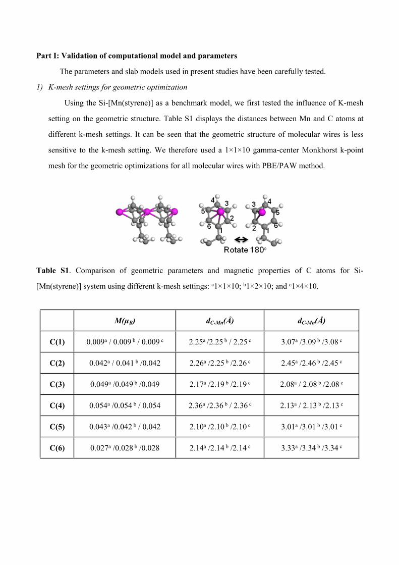
1) K-mesh settings for geometric optimization
Using the Si-[Mn(styrene)] as a benchmark model, we first tested the influence of K-mesh
setting on the geometric structure. Table S1 displays the distances between Mn and C atoms at
different k-mesh settings. It can be seen that the geometric structure of molecular wires is less
sensitive to the k-mesh setting. We therefore used a 1×1×10 gamma-center Monkhorst k-point
mesh for the geometric optimizations for all molecular wires with PBE/PAW method.
Table S1. Comparison of geometric parameters and magnetic properties of C atoms for Si-
[Mn(styrene)] system using different k-mesh settings: a1×1×10; b1×2×10; and c1×4×10.
M(µB) dC-Mn(Å) dC-Mn(Å)
C(1) 0.009a / 0.009 b / 0.009 c 2.25a /2.25 b / 2.25 c 3.07a /3.09 b /3.08 c
C(2) 0.042a / 0.041 b /0.042 2.26a /2.25 b /2.26 c 2.45a /2.46 b /2.45 c
C(3) 0.049a /0.049 b /0.049 2.17a /2.19 b /2.19 c 2.08a / 2.08 b /2.08 c
C(4) 0.054a /0.054 b / 0.054 2.36a /2.36 b / 2.36 c 2.13a / 2.13 b /2.13 c
C(5) 0.043a /0.042 b / 0.042 2.10a /2.10 b /2.10 c 3.01a /3.01 b /3.01 c
C(6) 0.027a /0.028 b /0.028 2.14a /2.14 b /2.14 c 3.33a /3.34 b /3.34 c

2) Effect of K-mesh setting and Si-layer thickness on the band structure
We have extensively investigated the band structure of silicon slab models with or without
styrene modifications using different k-mesh setting and different Si-layers.
We first tested the effect of k-mesh setting on the band structure of Si slab models (with and
without styrene modifications) and Si-[Mn(styrene)]. From Figure S1, it can be found that the band
structures are less sensitive to the k-mesh density. For the six-layer Si slab models with or without
styrene modifications, the different k-mesh setting leads to the same band gap values and band
structures.
(a)
(b)
Figure S1. Comparison of the energy band structures of (a) a six-layer H-passivated Si slab model and (b) a six-layer H-passivated Si slab model with styrene modification, using different k-mesh settings and HSE06 method.

However, it is found that the band gap of six-layer Si-slabs is much larger than the bulk silicon.
From the HSE06 results, both the six-layer Si-slabs have a quite large band gap around ~2.0 eV,
which is much larger than the bulk Si-crystal (~1.12 eV). We therefore further examined the band
structure of Si-slab models with different silicon layers. From Figure S2, it is found that when the Si-
layer is increased from 6 to 16, the band gap of Si-[styrene]∞ decreases to 1.35 eV. Several
theoretical and experimental studies have found the similar tendency. For example, Vazhappilly et al.
reported the HSE results of band gap of H-passivated Si(111) slabs [J. Phys. Chem. C 2014, 118,
4429−4436]. They found that the band gap of H-passivated Si(111) was 1.71, 1.50 and 1.45 eV,
respectively, using 4, 8 and 12 Si-layer models. Bassani et al. also found that the band gap of
nanocrystalline Si multilayers presented a large increase for decreasing Si layer thickness [Appl. Surf.
Sci. 1997, 117/118, 670-676].
Figure S2. Band structure of Si-[(styrene)]∞ with different layer of Si-atoms using the HSE06 functional. The k-mesh setting for band structure calculations is 1×1×10 plus additional 20 k-points along the Γ to X direction.
Despite of the band gap of silicon slab is significantly affected by the slab thickness, the
electronic structure properties of the molecular wires are less perturbed as the energy bands near to
the Fermi level are mainly contributed by the surface molecular wire. Figure S3 and S4 displays the
energy band structure of Si-[Mn(styrene)]∞ with or without neighboring H-atom defect and
[Mn(styrene)]∞-[Cr(styrene)]∞ with different slab thickness. It can be found that for Si-
[Mn(styrene)]∞ with neighboring H-atom defect and [Mn(styrene)]∞-[Cr(styrene)]∞, slab models
containing six- or ten-layer Si-atoms demonstrate very similar band structure and electronic
properties (FM metal or Half Metal). However, the band structure of Si-[Mn(styrene)]∞ is somewhat

sensitive to the Si-layer thickness. With the increase of silicon layer from 6 to 14, the band gap in
spin up and down channels was narrowed to 0.25 and 0.1 eV, respectively.
(a) Six-Layer Si-slab
(b) Ten-Layer Si-slab
Figure S3. Band structures of [Mn(styrene)]∞-[Cr(styrene)]∞ and Si-[Mn(styrene)]∞ with one row H-atom defect. (a) Six layer Si-slab. (b) Ten layer Si-slab. The k-mesh setting for band structure calculations is 1×1×10 plus additional 20 k-points along the Γ to X direction.

Figure S4. Band structures of Si-[Mn(styrene)]∞. The k-mesh setting for band structure calculations
is 1×1×10 plus additional 20 k-points along the Γ to X direction.
Based on above results, we think that for the Si/molecular wire systems that demonstrate
semiconductor or half-metallic properties, it is necessary to consider the effect of Si-layer thickness
so as to accurately describe the band structure near to the Fermi energy levels. As a result, in present
studies we first used a six-layer Si-slab model to determine the ground properties of Si-molecular
wire system. However, for certain systems which demonstrate semiconductor or half metal properties,
a 10-layer Si-slab model is used for the energy bands calculations. Without specific annotation, the
reported electronic properties in this work are derived from a ten-layer silicon slab model and the k-
mesh setting is 1×1×10 for density of state calculation and additional 20 k-points along the Γ→X
direction are added for energy band plot.

Figure S5. The distance between TM atom (TM = V, Cr and Mn) and C atoms in adjacent phenyl rings. The local magnetic moment on each C atom is displayed. These geometric parameters are obtained by the PBE/PAW calculations based on a six-layer Si-slab model.

(a)
300K
800K

1000K
1500K
(b)
Figure S6. (a) A reduced four-layer silicon substrate model was used in MD simulation. The two bottom silicon layers as well as bottom hydrogen atoms are fixed during MD simulations. (b)The evolution of total electronic energy (ET), kinetic energy (EK), total magnetic moment of unit cell (MM) and temperature during the 2.2ps simulations at different temperature. The MD simulations are carried using the PBE/PAW method for electronic energy calculation and the Nosé-Hoover method is used for temperature control. The time-step in MD simulations is 1fs.

Figure S7. The plotted spin density isosurface of [TM(styrene)]∞. Spin up and down densities are
distinguished by yellow and blue colors, respectively.

Figure S8. Band structure of various Si-[TM(styrene)]∞ SMWs predicted by PBE functional and PBE+U methods.

(a)
(b)Figure S9. (a) Because of the silicon substrate affects very slightly on the electronic and magnetic properties of the surface supported molecular wire, we therefore used a simplified gas phase molecular wire model with the silicon substrate is removed to understand the electronic structure of the doped Mn atom. Using this simplified model, we can get a more clear insight into the splitting behavior of Mn 3d orbital. The lattice constant c is 7.72 Å and the calculated magnetic moment of Mn atom in the gas phase wire (3.76 µB) is the same as that in surface supported wire. (b) The HSE06 band structure of gas phase Mn-styrene molecular wire.

Ti-HSE06 V-HSE06
(a) Band structure of Si-[Ti(styrene)]∞ and Si-[V(styrene)]∞ SMWs
V-V HSE06 Cr-Cr HSE06 Mn-Mn HSE06
(b) Band structure of [TM(styrene)]∞-[TM(styrene)]∞ DMWs
Figure S10. Band structure of various Si-[TM(styrene)]∞ SMWs and DMWs predicted by HSE06 functional based on a six-layer Si-slab model.

Table S1. Absolute electronic energies of defected [Mn(styrene)]∞ SMWs with different spin
configurations. Si ( i = 1 to 7) denotes local magnetic moment on each Mn atom. The configuration
of [Mn(styrene)]∞ SMWs is given in Fig. 6a in the context.
E (eV) S1 S2 S3 S4 S5 S6 S7
-1280.7525 3.063 1.922 -2.658 3.157 -2.621 2.067 -2.166
-1280.9925 2.947 3.161 -2.545 -3.183 2.572 -2.051 2.130
-1281.0698 -0.483 3.144 -1.360 -3.120 -3.116 1.813 -0.281
-1281.1027 3.110 3.081 -1.265 2.706 -3.254 -2.992 0.868
-1281.3832 2.107 2.369 -2.236 3.135 -1.416 3.055 2.105
-1281.5324 2.223 -2.326 -3.231 2.607 -2.079 3.030 2.163
-1281.5404 3.044 2.548 2.846 2.750 2.936 3.080 -0.847
-1281.5424 3.094 3.135 3.105 3.098 3.102 3.124 2.954
-1281.5644 -2.206 2.413 3.248 -2.442 2.510 3.023 2.382
-1281.5989 2.472 -3.084 2.302 -3.127 2.628 3.161 -0.799
-1281.6392 -2.308 2.371 -0.938 3.464 2.796 2.798 2.017
-1281.7352 2.216 -2.187 3.137 3.188 3.127 2.707 -2.274
-1281.7716 -2.214 2.388 3.205 3.135 3.088 -2.108 2.140
-1281.8475 -2.219 2.341 3.200 -2.655 2.819 2.544 -2.268
-1282.0956 -0.257 2.789 3.328 2.540 -3.136 2.789 2.328
-1282.2121 -2.221 2.356 3.221 3.095 3.159 0.210 0.080
-1282.2356 -2.312 2.347 2.737 2.047 3.151 3.084 -0.436


![Molecular Wires, Switches and Memories · devices, and memories. Molecular electronics [1-3] is conceptually different from conventional solid state semiconductor electronics. It](https://static.fdocuments.in/doc/165x107/5ecb1229c78cbc769f459166/molecular-wires-switches-and-memories-devices-and-memories-molecular-electronics.jpg)


