
MODULE TITLE : ELECTRONICS TOPIC TITLE : AMPLIFIERS LESSON ... · 12/3/2015 · ADJUSTABLE GAIN...
40
MODULE TITLE : ELECTRONICS TOPIC TITLE : AMPLIFIERS LESSON 3 : LINEAR APPLICATIONS OF OP AMPS EL - 3 - 3 © Teesside University 2012
Transcript of MODULE TITLE : ELECTRONICS TOPIC TITLE : AMPLIFIERS LESSON ... · 12/3/2015 · ADJUSTABLE GAIN...

MODULE TITLE : ELECTRONICS
TOPIC TITLE : AMPLIFIERS
LESSON 3 : LINEAR APPLICATIONS OF OP AMPS
EL - 3 - 3
© Teesside University 2012
Steve
Text Box
________________________________________________________________________________________
INTRODUCTION________________________________________________________________________________________
In this lesson, we start to use the operational amplifier as a functional block.
We have moved on from individual transistor circuits.
We shall investigate a number of circuits which can perform linear analytic
functions on signals, such as amplifying, adding, subtracting, filtering,
integrating and differentiating.
________________________________________________________________________________________
YOUR AIMS________________________________________________________________________________________
At the end of this lesson, you should be able to:
• analyse simple op amp circuits
• design simple active filters.
________________________________________________________________________________________
STUDY ADVICE________________________________________________________________________________________
You may find it quite useful to make a separate summary of all the op amp
circuits we investigate, together with just their function and basic equation; it
acts as an aide memoire.
The most common error in applying the formulae derived in this lesson is
carelessness with signs. Remember that, if I ask you for the output voltage of
an amplifier, or the gain of an amplifier, the sign is part of the answer!
1
Teesside University Open Learning(Engineering)
© Teesside University 2012
Steve
Text Box

________________________________________________________________________________________
BASIC APPLICATIONS________________________________________________________________________________________
In the previous lesson, we introduced the basic ideal operational amplifier. In
this lesson, we shall be building up a library of applications. We shall assume
a perfect amplifier; i.e. one which has infinite gain, no input current and
infinite bandwidth. In practice of course, no amplifier is ideal and, in the next
lesson, we shall try to see what effects the imperfections cause.
Remember the basic formula for the gain of the op amp in inverting mode.
INVERTER
FIG. 1
This is a special case of the basic application we looked at in the last lesson;
here the two resistors R1 and R2 are the same.
V
V
R
Ro
in
= = −– 1 ........................................ ( )2
R
Vin
R
Vo
0 V
–+
V
V
R
Ro
in
= – 2
1
................................................ ( )1
2
Teesside University Open Learning(Engineering)
© Teesside University 2012
Steve
Text Box

ADJUSTABLE GAIN CIRCUITS OR SCALERS
In many cases, we may want adjustable gain. Of course, one can replace either
R1 or R2 by a variable resistance, but the following circuits have some
advantages. In these circuits, we take an adjustable fraction, x, of the input or
the output. Obviously, x is less than or equal to 1.
FIG. 2(a) and (b)
From FIGURE 2(a), we obtain the following relationship.
This is just an application of the fundamental gain rule of the op amp.
For FIGURE 2(b), assume the point V1 is a virtual earth.
V
R
xV
R
V
V x
R
R
in o
o
in
– –
–
0 0
1
1 2
2
1
=
= ........................................... ( )4
V
Vx
R
Ro
in
= – 2
1
........................................... ( )3
(a) (b)
R
Vin
Vo
0 V
–+
R1
R2
xVin
0 V
Vin Vo
0 V
–+
R1
R2
V1
RxVo
0 V
3
Teesside University Open Learning(Engineering)
© Teesside University 2012
Steve
Text Box

These formulae assume that R1 and R2 are much greater than the potentiometer
resistance R.
In Figure 2(b), what happens if x is set to 0?
....................................................................................................................................................
....................................................................................................................................................
....................................................................................................................................................
________________________________________________________________________________________
If x → 0, gain tends to A, the gain of the op amp (not infinity in practice!).
From a practical point of view, it is often desirable to prevent x going to 0 by
including a fixed resistor in series with the potentiometer.
WORKED EXAMPLE 1
In the circuit of FIGURE 3, find the exact gain.
FIG. 3
Vin Vo
0 V
–+R1
0 V
R2
100 kΩ
1 kΩ
R310 kΩ
R4
100 kΩ
4
Teesside University Open Learning(Engineering)
© Teesside University 2012
Steve
Text Box

We could use equation (4) if x can be deduced. Now, an approximate answer
would give x as , but this does not take into account the loading
effect of R2. Because V– is a virtual earth, R2 is effectively in parallel with R4.
This leads to the following expression for x.
Hence, gain is calculated from equation (4) as follows.
Put in the values given in FIGURE 3.
If we had used x as , the gain would have been calculated as –1010.
This is quite a useful circuit, because we have achieved a high gain without
using very high resistance ratios, or making R1 very low.
R
R R4
3 4+( )
Gain = ⎛⎝⎜
⎞⎠⎟
+( ) + ×( )–
1010
10 10 10 10 10
10
5
4
5 3 5 3 5
3 ××⎛
⎝⎜⎞
⎠⎟
=
10
1020
5
–
Gain =+
=+( ) +
–
–
R
R
R R R
R R
R
R
R R R R R
R
2
1
3 4 2
4 2
2
1
3 4 2 4 2
4 RR2
xR R
R R R=
+4 2
3 4 2
R
R R4
3 4+( )
5
Teesside University Open Learning(Engineering)
© Teesside University 2012
Steve
Text Box

SUMMER
FIG. 4
Since input current = feedback current, we can write the following equation.
The circuit gives the inverted algebraic sum of all input signals and can, of
course, be extended to any number of inputs.
For Vin1 = +1 V, Vin2 = –2 V, Vin3 = +3 V, R2 = 10 kΩΩ, Ri1 = 1 kΩΩ, Ri2 = 1.5 kΩΩ and
Ri3 = 10 kΩΩ, find Vo.
....................................................................................................................................................
....................................................................................................................................................
....................................................................................................................................................
....................................................................................................................................................
....................................................................................................................................................
________________________________________________________________________________________
The value of Vo is +0.33 V.
VR
RV
R
RV
R
RVo
iin
iin
iin= + +
⎡
⎣⎢
⎤
⎦⎥– 2
11
2
22
2
33 ................. ( )5
Vin1
Vo
0 V
–+
R2
Vin2
Vin3
Ri1
Ri2
Ri3
6
Teesside University Open Learning(Engineering)
© Teesside University 2012
Steve
Text Box

DIFFERENTIAL AMPLIFIER
FIG. 5
Assume that the amplifier is ideal.
Note that V1 is not a virtual earth, since V2 is not 0 V. V1 is here virtually equal
to V2.
V V
R
V V
Rin o1 1
1
1
2
– –= ..............................................
.
( )
–
6
2 2
3
2
4
V V
R
V
Rin = .....................................................
.......................
( )7
1V V= ................................. ( )8
Vin1
Vo
0 V
–+
R2
Vin2
R4
R1
R3
V1
V2
7
Teesside University Open Learning(Engineering)
© Teesside University 2012
Steve
Text Box

Rearrangement of equation (7) allows us to determine V2.
We could have deduced this straight from the diagram. How?
....................................................................................................................................................
....................................................................................................................................................
________________________________________________________________________________________
Because it is just a voltage divider.
Rearrangement of equation (6) yields the equation below.
Since V1 = V2, and substituting for V2 from equation (9), we can obtain an
equation with V1 and V2 eliminated.
This can then be arranged to express the output voltage in terms of the input
voltages.
V
R
V
RV
R R R
R R R Rin o
in1
1 22
4 1 2
3 4 1 2
= ++( )
+( )–
V
R
V
RV
R Rin o1
1 21
1 2
1 1= + +⎡
⎣⎢
⎤
⎦⎥
V
RV
R R
R V V R R
VR
in
in
2
32
3 4
4 2 2 4 3
24
1 1= +⎡
⎣⎢
⎤
⎦⎥
= +( )
=VV
R Rin2
4 3+ ........................................... ( )9
8
Teesside University Open Learning(Engineering)
© Teesside University 2012
Steve
Text Box

As we would expect, the output depends on both Vin1 and Vin2.
Choice of the resistors can considerably simplify this equation.
If
then the equation simplifies to that below in equation (11).
So now we have a differential amplifier with a well defined gain.
If Vin1 + 3 V, Vin2 = +4 V, R1 = 1 kΩΩ and R2 = R3 = R4 = 10 kΩΩ, find Vo.
....................................................................................................................................................
....................................................................................................................................................
....................................................................................................................................................
....................................................................................................................................................
....................................................................................................................................................
....................................................................................................................................................
________________________________________________________________________________________
The value of Vo is –8 V.
VR
RV Vo in in= ( )– –2
11 2 .............................. ( )11
R
R
R
R1
2
3
4
=
VR
RV V
R
R
R
R
o in in=+
⎛⎝⎜
⎞⎠⎟
+⎛⎝⎜
⎞⎠⎟
⎡
⎣
– –2
11 2
1
2
3
4
1
1
⎢⎢⎢⎢⎢⎢
⎤
⎦
⎥⎥⎥⎥⎥
........... ( )10
9
Teesside University Open Learning(Engineering)
© Teesside University 2012
Steve
Text Box

NON-INVERTING AMPLIFIER
FIG. 6
From equation (10) and putting Vin1 = 0, R3 = 0 and replacing R4 by an open
circuit (∞), we obtain the following simple relationship.
This gives us a non-inverting amplifier; i.e. the gain is positive. The minimum
gain is 1! With the inverting amplifier, we can get gains less than 1.
BUFFER
FIG. 7
From equation (12), with R1 = ∞ and R2 = 0, we have the special case of a
buffer.
V Vo in= 2 ............................................. ( )13
Vo–+Vin2
V
V
R
Ro
in2
2
1
1= + ............................................. ( )12
Vo–+
R2
Vin2
R10 V
10
Teesside University Open Learning(Engineering)
© Teesside University 2012
Steve
Text Box

REVIEW OF CIRCUITS EXAMINED
We have built up a repertoire of circuits which can:
• give high programmable negative or positive gains
• add or subtract multiple inputs
• provide buffer amplifiers with gains of +1 or –1.
________________________________________________________________________________________
FREQUENCY DEPENDENT CIRCUITS________________________________________________________________________________________
INTRODUCTION
FIG. 8
When we consider sine waves, operational amplifiers can be used as active
filters to provide amplification or attenuation and/or phase-shift for selected
frequency ranges of the input signal. The usual advantages of operational
amplifiers are retained.
These advantages are that the gain is:
• defined accurately by the ratio of impedances
• independent of the load.
Vin
Vo–+
Z2
Z1
0 V
11
Teesside University Open Learning(Engineering)
© Teesside University 2012
Steve
Text Box

Equation (14) below gives the general relationship.
G(jω) is the gain expressed as a frequency dependent complex number, and
can be plotted on a Bode Diagram.
In general, the output is a sine wave with the same frequency as the input, but
with a different amplitude and displaced in phase. By choosing Z1 and Z2
appropriately, we can design low-pass, high-pass and band-pass filters. The
filters can be cascaded to give second and higher order filters, discussion of
which is beyond the scope of this module.
Let us compare a basic first-order low-pass filter with a similar active filter.
LOW-PASS FILTER
(a) Passive Filter
The circuit is shown in FIGURE 9(a).
where
and
Z
R
C
RC
R
CR
Z R R
L
L
L
L
s
2
1
1 1=
+=
+
= +
j
jj
ω
ωω
V
V
Z
Z Zo
s
=+2
2 1
V
VG
Z
Zo
in
j
jj
j
j ........
ωω
ωωω
( )( ) = ( ) =
( )( )– 2
1
......... ( )14
12
Teesside University Open Learning(Engineering)
© Teesside University 2012
Steve
Text Box

So
(b) Active Filter
The circuit is shown in FIGURE 9(b).
FIG. 9 Passive and Active Filter
Vo–+
C
R1Rs
R2
Vs
RL
Source Filter Load
Rs
Vs
RLC
Source Filter Load
R
Vo
Z2
V
V
RC
R R
Z
Z
R
R R
o
s s
s
=+
=⎛⎝⎜
⎞⎠⎟
=+( ) +
––
–
2
1
2
1
2
1
1
1
j
j
ω
ωωCR2( )
V
V
R
CRR
CRR R
R
R
o
s
L
Ls
L
L
=+( )
++ +
⎧⎨⎩
⎫⎬⎭
=
–
–
112
2jj
ωω
++ +( ) ++⎡⎣ ⎤⎦
+ +( )⎧⎨⎪
⎩⎪
⎫⎬⎪
⎭⎪R R
CR R R
R R RsL s
L s
1jω
13
Teesside University Open Learning(Engineering)
© Teesside University 2012
Steve
Text Box

We now draw the conclusions shown in FIGURE 10.
FIG. 10
It is clear that active filters can be designed so that they are largely
independent of source and load impedances, and that they can be designed to
have any desired gain.
In general, active filters can be designed to use smaller values of capacitance
(cheaper) and to avoid the use of inductors which are heavy and bulky, and
often lead to electrical interference and audible noise.
DC Gain
InputResistance
Passive Active
Always < 1
Depends on Rs and RLas well as R and C
Depends only onC and R2
Normally it iseasy to chooseR1 » Rs
NormallyRs < R < RLotherwise there areloading problems asRs + RL changes.
But this is sometimesdifficult to achieve.
Bandwidth
=1
CR
Depends on load RL
Can be
programmedby R2
Rs + R1( )
14
Teesside University Open Learning(Engineering)
© Teesside University 2012
Steve
Text Box

However, active filters can only be used for signal conditioning; they cannot
be used in the filtering of high power circuits.
INTEGRATOR
This is the first of two special frequency dependent circuits which will now be
investigated.
FIG. 11
Since input current = feedback current, use of the basic relationship for a
capacitor gives the following equation.
Integrate both sides with respect to t.
VV
RCto
in=⌠
⌡
⎮⎮⎮⎮
– d ...................................... ( )15
V
RC
V
tin o– –0 0
=( )d
d
Vin
Vo–+
C
R
0 V
15
Teesside University Open Learning(Engineering)
© Teesside University 2012
Steve
Text Box
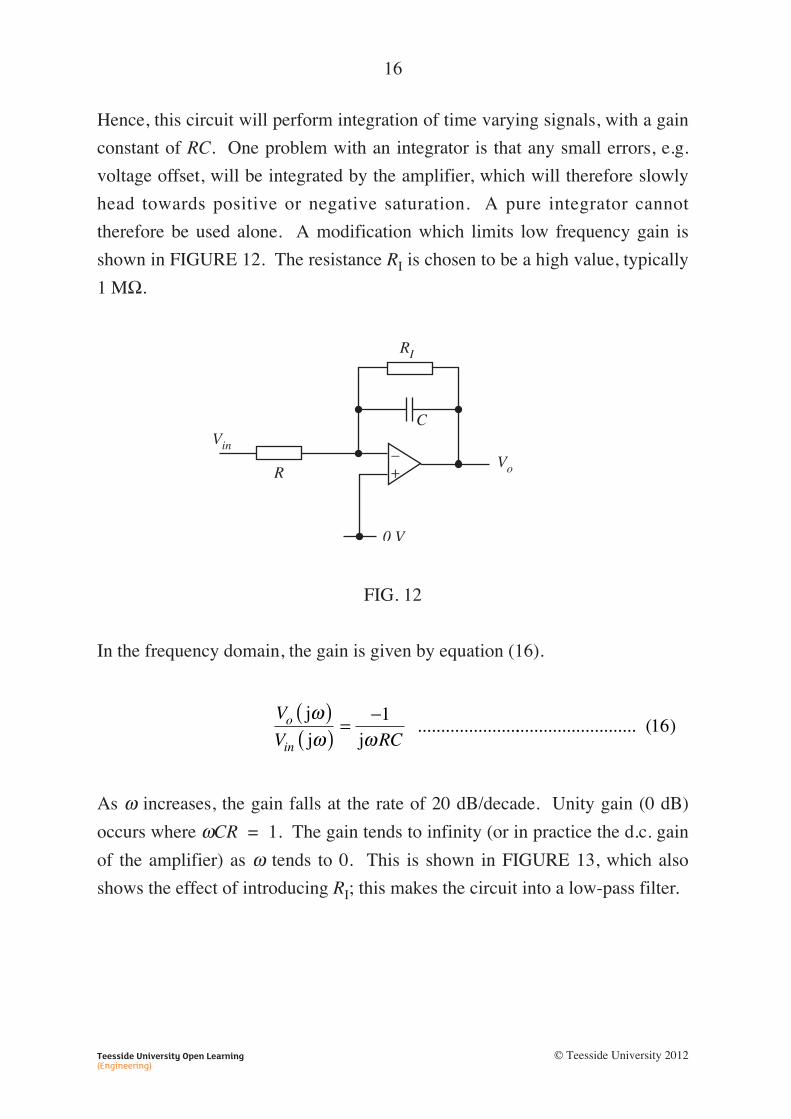
Hence, this circuit will perform integration of time varying signals, with a gain
constant of RC. One problem with an integrator is that any small errors, e.g.
voltage offset, will be integrated by the amplifier, which will therefore slowly
head towards positive or negative saturation. A pure integrator cannot
therefore be used alone. A modification which limits low frequency gain is
shown in FIGURE 12. The resistance RI is chosen to be a high value, typically
1 MΩ.
FIG. 12
In the frequency domain, the gain is given by equation (16).
As ω increases, the gain falls at the rate of 20 dB/decade. Unity gain (0 dB)
occurs where ωCR = 1. The gain tends to infinity (or in practice the d.c. gain
of the amplifier) as ω tends to 0. This is shown in FIGURE 13, which also
shows the effect of introducing RI; this makes the circuit into a low-pass filter.
V
V RCo
in
j
j j .....................
ωω ω
( )( ) = −1
........................... ( )16
Vin
Vo–+
C
R
RI
0 V
16
Teesside University Open Learning(Engineering)
© Teesside University 2012
Steve
Text Box

FIG. 13
DIFFERENTIATOR
FIG. 14
Vin
Vo–+
C
R
0 V
0
Gain(dB)
Effect of RI
–20 dB/decade
Frequencydecade
10m 10m+1
ω = 1CR
Log10ω
17
Teesside University Open Learning(Engineering)
© Teesside University 2012
Steve
Text Box

Assuming an ideal op amp, the following equation holds.
This represents an ideal differentiator, but it is rarely used in this form.
In the frequency domain, the gain is given by equation (18)
Note that the gain increases as frequency!
This property which the differentiator has of amplifying any high frequency
signal means that any 'noise' in the input is also greatly amplified; and the
higher the noise frequency, the greater the gain. A modification to reduce the
gain at high frequencies is shown in FIGURE 15, which also shows the
frequency response.
G CRj j ..............................ω ω( ) = − ...................... ( )18
CV
t
V
R
V RCV
t
in o
oin
d
d
Sod
d ...............
=−
= − ................................. ( )17
18
Teesside University Open Learning(Engineering)
© Teesside University 2012
Steve
Text Box

FIG. 15
Feedback Impedancej j
Input I
= =+
RC
R
C R22
2
2 2
11ω ω
mmpedancej
j
j
Soj
j
= + =+
( )
RC
C R
C
V
Vo
in
11
1 1
1
1 1
ωω
ω
ωωω
ωω ω( ) =
+( ) +( )–j
j j .........
C R
C R C R1 2
1 1 2 21 1................. ( )19
Vin
Vo–+
0 V
R1C1
C2
R2
0
Gain(dB)
+20 dB/decade
Response withoutR1 and C2
ω = 1C1R2
Log10ω
–20 dB/decade
ω = 1C2R2 ω = 1
C1R1
R1= 0
19
Teesside University Open Learning(Engineering)
© Teesside University 2012
Steve
Text Box
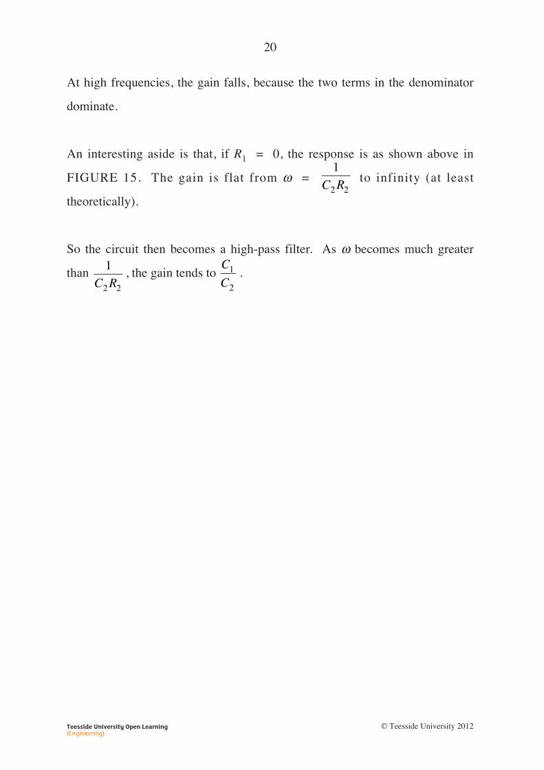
At high frequencies, the gain falls, because the two terms in the denominator
dominate.
An interesting aside is that, if R1 = 0, the response is as shown above in
FIGURE 15. The gain is flat from ω = to infinity (at least
theoretically).
So the circuit then becomes a high-pass filter. As ω becomes much greater
than , the gain tends to .C
C1
2
1
2 2C R
1
2 2C R
20
Teesside University Open Learning(Engineering)
© Teesside University 2012
Steve
Text Box

________________________________________________________________________________________
NOTES________________________________________________________________________________________
...................................................................................................................................................
...................................................................................................................................................
...................................................................................................................................................
...................................................................................................................................................
...................................................................................................................................................
...................................................................................................................................................
...................................................................................................................................................
...................................................................................................................................................
...................................................................................................................................................
...................................................................................................................................................
...................................................................................................................................................
...................................................................................................................................................
...................................................................................................................................................
...................................................................................................................................................
...................................................................................................................................................
...................................................................................................................................................
...................................................................................................................................................
...................................................................................................................................................
...................................................................................................................................................
...................................................................................................................................................
...................................................................................................................................................
...................................................................................................................................................
...................................................................................................................................................
...................................................................................................................................................
...................................................................................................................................................
...................................................................................................................................................
...................................................................................................................................................
...................................................................................................................................................
...................................................................................................................................................
...................................................................................................................................................
21
Teesside University Open Learning(Engineering)
© Teesside University 2012
Steve
Text Box

________________________________________________________________________________________
SELF-ASSESSMENT QUESTIONS________________________________________________________________________________________
1. Find the output voltage Vo of the following circuits. REMEMBER
THAT SIGNS ARE IMPORTANT!
Vo–+
0 V
10 kΩ
1 kΩ
–1 VVo
–+
0 V
15 kΩ
1 kΩ–0.5 V
Vo–+
0 V
100 kΩ
–100 V
Vo–+
0 V
15 kΩ1 kΩ–0.5 V
1.5 kΩ
12 kΩ
10 kΩ
+2 V
–4 V
–3 V
(a) (b)
(c) (d)
100 kΩ1MΩ
100 kΩ
VX
22
Teesside University Open Learning(Engineering)
© Teesside University 2012
Steve
Text Box

2. What is the gain in each of the following circuits?
3. Design an amplifier circuit which gives an output of +10 V when the
input is –2V, and has an output of 0 V when the input is –6 V.
Hint: Sketch the gain line, get an equation for the straight line and then
match the equation with one of the circuits we have developed. You can
use one or two amplifiers and you will need a reference voltage.
Vo–+
0 V
10 kΩ
1 kΩ
Vo–+
0 V
10 kΩ
1 kΩ
Vo–+
0 V
100 kΩ
Vo–+
0 V
20
(a) (b)
(c)
(d)
100 kΩ
10 kΩ
10 kΩ
0 V
Vin
10 kΩ
0 V
Vin
1 kΩ
10 kΩ
20 kΩ20 kΩ
20 kΩ10 kΩ20 kΩ
Vin
VX VY
100 kΩ
–+
0 VVin
VX
10 kΩ
100 kΩ
23
Teesside University Open Learning(Engineering)
© Teesside University 2012
Steve
Text Box

4. Find the peak output of the amplifier shown below.
Hint: How do you find the maximum of a signal?
5.
Show that the expression for gain in the circuit above is
GCR
CRj
j
jω
ωω
( ) =+1 2
1
Vo
0 V
–+R1
Vin
R2C
R2 sin β
R
Vo
0 V
–+3 sin 2β
2R
24
Teesside University Open Learning(Engineering)
© Teesside University 2012
Steve
Text Box

6. Sketch the shape of the outputs of (i) an op amp integrator and (ii) a
differentiator to the following input wave-forms.
Hint: Remember the definitions of integration and differentiation.
7. Design an active low-pass filter with a low frequency gain of –15 and a
bandwidth of 400 radians/second.
8. Obtain the gain expression for the circuit opposite. Show that the
magnitude of the gain is +1 for all frequencies.
Hint: you can use a modified gain expression from one of the circuits we
have already derived, or you can obtain the gain from first principles.
0A
A
T T
t
0A t
0
A
tA
Sine wave
(a)
(b)
(c)
25
Teesside University Open Learning(Engineering)
© Teesside University 2012
Steve
Text Box

Vin Vo
0 V
–+
R
C
R
R
26
Teesside University Open Learning(Engineering)
© Teesside University 2012
Steve
Text Box

________________________________________________________________________________________
SELF-ASSESSMENT QUESTIONS________________________________________________________________________________________
1. (a) Apply equation (1) for the gain of an inverting amplifier.
(b) Apply equation (12) for the gain of a non-inverting amplifier.
(c) Apply the Summer equation.
(d) It is easy to see that
V V Vo x x= − ⎛⎝⎜
⎞⎠⎟ = −100
100
Vo = ⎛⎝⎜
⎞⎠⎟ −( ) + ⎛
⎝⎜⎞⎠⎟ ( ) + ⎛
⎝⎜⎞⎠
151
0 5151 5
21512
.. ⎟⎟ −( ) + ⎛
⎝⎜⎞⎠⎟ −( )⎡
⎣⎢⎤⎦⎥
= − + − −[ ]
41510
3
7 5 20 5 4 5. .
== − 3V
VR
RVo in= +
⎛⎝⎜
⎞⎠⎟
= +⎛⎝⎜
⎞⎠⎟ ( ) =
1
1101
1 11
2
12
– – V
VR
RVo in=
⎛⎝⎜
⎞⎠⎟
= ⎛⎝⎜
⎞⎠⎟ ( ) = +
–
– – . .
2
1
151
0 5 7 5V
27
Teesside University Open Learning(Engineering)
© Teesside University 2012
Steve
Text Box

We have to find Vx. Because V1 is a virtual earth, the input circuit
becomes a voltage divider, in which the resistance of the two 100 kΩresistors in parallel is 50 kΩ. This is shown below.
Hence,
2. (a) We can use the differential amplifier formula, putting Vin1 = 0.
VR
RV
R
R
R
R
o in= −+
⎛⎝⎜
⎞⎠⎟
+⎛⎝⎜
⎞⎠⎟
⎡
⎣
⎢⎢⎢
2
12
1
2
3
4
0
1
1
–
⎢⎢⎢
⎤
⎦
⎥⎥⎥⎥⎥
= ++⎛
⎝⎜⎞⎠⎟
+( )
= +
101
110
1 1
5 5
2
2
V
V
in
in.
Vo = + 4 76. V
Vx = ×+ ×
−( )
= −
50 1010 50 10
100
4 76
3
6 3
. V
1 MΩ
100 kΩ
–100 V
100 kΩ
0 V
Vx
28
Teesside University Open Learning(Engineering)
© Teesside University 2012
Steve
Text Box

(b) Use the formula derived in Worked Example 1.
(c) This is an extension of the circuit of Question 1(d).
We now find by a similar process. See the circuit below.
20 kΩ
0 V
Vx
Vin
20 kΩ 10 kΩ
20 kΩ 20 kΩ
V
Vx
in
V
V
V
V
o
y
y
x
= −
=Ω Ω
Ω Ω + Ω
=
1
12
20 k 20 k
20 k 20 k 10 k
treati[ nng the circuit as a divider]
Gain =+( ) +
=+( ) +
–
–
R
R
R R R R R
R R2
1
3 4 2 4 2
4 2
101
10 1 10 100
10
120= −
29
Teesside University Open Learning(Engineering)
© Teesside University 2012
Steve
Text Box

The overall gain is calculated as follows.
(d) For the inverting amplifier,
For the differential amplifier,
V V V
V V
V
o x in
in in
i
= − −( )
= − −⎡⎣ ⎤⎦ −( )
= − −
10
10 10
10 11 nn
inV
( )
= + 110
V Vx in= − 10
V
V
V
V
V
V
V
Vo
in
o
y
y
x
x
in
=
= −( ) ⎛⎝⎜
⎞⎠⎟
⎛⎝⎜
⎞⎠⎟
= −
112
13
166
V
Vx
in
=Ω Ω + Ω Ω( )
Ω Ω + Ω Ω(20 k k 20 k 20 k
20 k k 20 k 20 k
10
10 )) + Ω
=
20 k
13
30
Teesside University Open Learning(Engineering)
© Teesside University 2012
Steve
Text Box

3. The two input/output conditions define two points on a straight line, the
graph of which is sketched overleaf; the equation of the line is
The gain is positive.
There are many possible solutions.
Solution by Adapting a Differential Amplifier
From equation (10), we can see that the input in this case must be Vin2, because
of the positive gain requirement.
Try putting R3 = 0 and R4 as an open circuit. Then use equation (10).
VR
RV V
R
R
R
R
o in in=⎛⎝⎜
⎞⎠⎟
+ +⎛⎝⎜
⎞⎠⎟
⎛
⎝⎜⎞
⎠⎟
=
2
11
1
2
2
1
111
2
1
1⎛⎝⎜
⎞⎠⎟
+ +⎛⎝⎜
⎞⎠⎟
⎛
⎝⎜⎞
⎠⎟V V
R
Rin in
Vin
Vo
+10
–6 –2
V Vo in= +2 5 15.
31
Teesside University Open Learning(Engineering)
© Teesside University 2012
Steve
Text Box

Making this identical with the target equation gives two conditions.
The second of these conditions gives = 1.5.
Choose R2 = 15 kΩ and R1 = 10 kΩ from the E12 series to satisfy this
condition.
The first condition then gives the following equation.
Hence,
The circuit is shown below.
–10 V 10 kΩ
Vo–+
Vin
15 kΩ
R1
R2
Vin1 10= − V
− ( ) = +1 5 151. Vin
R
R2
1
−⎛⎝⎜
⎞⎠⎟
= + + =R
RV
R
Rin2
11
2
1
15 1 2 5and .
32
Teesside University Open Learning(Engineering)
© Teesside University 2012
Steve
Text Box

Solution by Using Two Amplifers
The first amplifier gives a gain of –2.5.
The second is a summer with a gain of –1.
4. This is a fairly difficult question. First get an expression for the output.
Differentiate with respect to β.
d
d
[Usin
Vo
ββ β
β β
= −
= − ( )
2 3 2
2 3 2 12
cos – cos
cos – cos – gg double angle formula]
Vo = − 2 1 5 2sin – . sinβ β
V V
V
V
V
o x
x
in
in
= − ( )
= − +
= − −( ) +
= + +
–
.
.
15
15
2 5 15
2 5 15
Vo–+
–+
100 kΩ10 kΩ
0 V
10 kΩ
0 V 10 kΩ–15 V
Vx
39 kΩ1 kΩVin
33
Teesside University Open Learning(Engineering)
© Teesside University 2012
Steve
Text Box

The peak of the output will be where = 0.
Solve this quadratic for cos β.
Hence,
Not all these are maxima; if you sketch the wave-forms of 2sinβ and
1.5sin2β and add them, you will see that the solutions we want are given
by ±55.9°.
Hence,
5. The complex gain is given by –
In this case, we have the following values of Z1 and Z2.
Hence, G
RC
R
CR
CRj
j j
jω
ω ωω
( ) =+
⎛⎝⎜
⎞⎠⎟
=+( )
– –2
1
2
1
11
Z RC
Z R2 2 1 11= + =
jand
ω
Z
Z2
1
Vo (max)
V
At
= − ( ) ×( )
= −
2 55 9 1 5 2 55 9
3 05
sin . – . sin .
.
ββ = − = +55 9 3 05. , .Vo (max) V
β = ± ° ± °55 9 153 3. .or
cos
. .
β = − ± −
= −
2 4 7212
0 56 0 89or
2 6 3 02cos cos –β β+ =
d
d
Vo
β
34
Teesside University Open Learning(Engineering)
© Teesside University 2012
Steve
Text Box

6. Integration Response Differentiation Response
The total area under a graph The slope of a graph
(Remember the – sign!)
(a)
t t
∞
(b)
t t
∞
(c)
t
0
+cos
t0
–cos
35
Teesside University Open Learning(Engineering)
© Teesside University 2012
Steve
Text Box

7. The gain of an active low-pass filter is given by the equation below (see
notes).
We require a d.c. gain of –15. Hence = 15.
We also require that ωCR2 = 1 when ω = 400.
It is best to make C small and R large, so try C = 10 nF.
Therefore,
Select R2 = 270 kΩ as the nearest value in the E12 series.
Finally,
Select R1 = 18 kΩ, which is a standard value in the E12 series.
8. We can adapt the differential amplifier formula, equation (10), by putting
V V V R R R R RCin in in1 2 2 3 4= = = = = =, and
1j1 ω
RR
12
3
15270
1015
18= = × = kΩ
R28 1
400 10 250= ×( ) =− −kΩ
R
R2
1
GR
R CRj
jω
ω( ) = =
+– 2
1 2
11
36
Teesside University Open Learning(Engineering)
© Teesside University 2012
Steve
Text Box
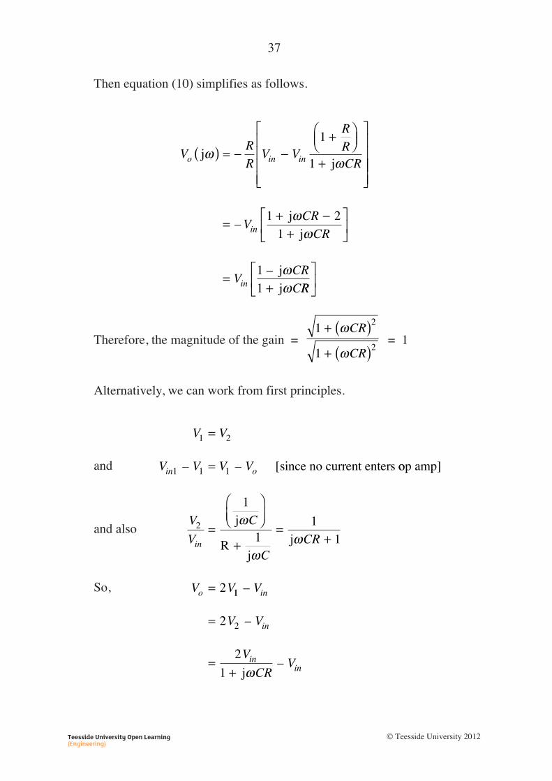
Then equation (10) simplifies as follows.
Therefore, the magnitude of the gain = = 1
Alternatively, we can work from first principles.
and
and also
So,
V V
V V V Vin o
1 2
1 1 1
=
=– – [since no current enters oop amp]
j
Rj
j
V
V
C
CCR
V V
in
o
2
1
11
1
2
=
⎛⎝⎜
⎞⎠⎟
+=
+
=
ω
ωω
11
22
2
1
–
–
–
V
V V
V
CRV
in
in
inin
=
=+ jω
1
1
2
2
+ ( )+ ( )
ω
ω
CR
CR
VR
RV V
R
RCRo in inj
jω
ω( ) = − −
+⎛⎝⎜
⎞⎠⎟
+
⎡
⎣
⎢⎢⎢⎢
⎤
⎦
⎥⎥
1
1 ⎥⎥⎥
= + −+
⎡
⎣⎢
⎤
⎦⎥
=+
–
–
VCR
CR
VCR
C
in
in
1 21
11
jj
jj
ωω
ωω RR
⎡
⎣⎢
⎤
⎦⎥
37
Teesside University Open Learning(Engineering)
© Teesside University 2012
Steve
Text Box

Finally,V
V
CR
CR
CR
CR
o
in
=− +( )
+
=+
2 1
1
11
j
j
jj
ωω
ωω
–
38
Teesside University Open Learning(Engineering)
© Teesside University 2012
Steve
Text Box

________________________________________________________________________________________
SUMMARY________________________________________________________________________________________
The operational amplifier has proved to be a versatile implement in the design
of a wide range of linear circuits.
The lesson has developed the theory of d.c. amplifier circuits for the:
• inverter
• scaler
• summer
• differential amplifier
• non-inverting amplifier
• buffer.
We have also investigated frequency dependent circuits for the:
• low-pass filter
• integrator
• differentiator.
Many more circuits are possible and, indeed, a comprehensive treatment of
active filters alone could easily run to a full module. This lesson has provided
the groundwork.
39
Teesside University Open Learning(Engineering)
© Teesside University 2012
Steve
Text Box