Modulateur passe-haut et application dans la réception ... · Modulateur ∆ passe-haut et...
209
HAL Id: pastel-00006055 https://pastel.archives-ouvertes.fr/pastel-00006055 Submitted on 10 May 2010 HAL is a multi-disciplinary open access archive for the deposit and dissemination of sci- entific research documents, whether they are pub- lished or not. The documents may come from teaching and research institutions in France or abroad, or from public or private research centers. L’archive ouverte pluridisciplinaire HAL, est destinée au dépôt et à la diffusion de documents scientifiques de niveau recherche, publiés ou non, émanant des établissements d’enseignement et de recherche français ou étrangers, des laboratoires publics ou privés. Modulateur Σ∆ passe-haut et application dans la réception multistandards Hasham Ahmed Khushk To cite this version: Hasham Ahmed Khushk. Modulateur Σ∆ passe-haut et application dans la réception multistandards. Electronique. Télécom ParisTech, 2009. Français. <pastel-00006055>
Transcript of Modulateur passe-haut et application dans la réception ... · Modulateur ∆ passe-haut et...
HAL Id: pastel-00006055https://pastel.archives-ouvertes.fr/pastel-00006055
Submitted on 10 May 2010
HAL is a multi-disciplinary open accessarchive for the deposit and dissemination of sci-entific research documents, whether they are pub-lished or not. The documents may come fromteaching and research institutions in France orabroad, or from public or private research centers.
L’archive ouverte pluridisciplinaire HAL, estdestinée au dépôt et à la diffusion de documentsscientifiques de niveau recherche, publiés ou non,émanant des établissements d’enseignement et derecherche français ou étrangers, des laboratoirespublics ou privés.
Modulateur Σ∆ passe-haut et application dans laréception multistandards
Hasham Ahmed Khushk
To cite this version:Hasham Ahmed Khushk. Modulateur Σ∆ passe-haut et application dans la réception multistandards.Electronique. Télécom ParisTech, 2009. Français. <pastel-00006055>
Thèse
présentée pour obtenir le grade de docteur
de l’Ecole Nationale Supérieure des Télécommunications
Spécialité : Electronique et Communications
Hasham Ahmed KHUSHK
Modulateur Σ∆ passe-hautet application dans la réception
multistandards
Soutenance le 27 novembre 2009 devant le jury composé de
Philippe Benabes Rapporteurs
Dominique Dallet
Patrick Garda Examinateurs
Dominique Morche
Patrick Loumeau Directeurs de thèse
Van Tam Nguyen


3
To my parents, my brothers and sisters.

4

5
Acknowledgements
This PhD has been performed in the auspices of group SIAM (Systèmes Intégrés Analogiqueset Mixtes) of Department COMELEC (Communications & Électronique) of Telecom-ParisTech. The three years of graduate studies here have brought about a remarkablepositive change in my attitude towards problem solving. I have learned the essence ofresearch and development and at the same time I have developed a firm belief in the farreaching capabilities of mankind. This has been possible by working and interacting witha group of very intelligent, resourceful and kind personalities. Surely without them, mystay in Telecom-ParisTech would not be as fruitful.
First and foremost, I would like to express my most sincere gratitude to my immediateadvisor, Doctor Van Tam Nguyen, who accepted me as his first doctoral candidate, showedconfidence in me and gave me numerous advice in academics, research and career. He isa person of great scientific acumen and admirable human values. He was by my sidethroughout the three years and taught me how to find paths in the dark alleys of research.I extend my utmost thankfulness to my PhD director, Professor Patrick Loumeau for hisguidance and encouragement. His experience and expertise in the subject are matchless.Having a highly diverse knowledge base, his suggestions were of immense importance. Hewas of great help in getting out of many complex circumstances. I take great pride inhaving worked with these two gentlemen, who are the specialists in the domain of dataconverters. I have learned a lot from them.
I am indebted to Hussein Fakhoury for his keen interest in my research and for thelengthy and productive discussions on the subject. His profound knowledge and extensiveexperience in the area of Analog IC Design coupled with his helping nature proved to be atreasure for me. Without his designed op-amps it would not have been possible to validatemy modulator designs.
I am extremely grateful to the members of my jury who gave their consent to analyzeand consequently validate my work. I feel honored that my work got approved by suchwell renowned specialists.
The moments spent with many peers is perhaps one of the best memories that I will takewith me of my graduate studies. I have very much enjoyed being in the company of friendslike Sumanto, Chadi, Farhan, Shivam, Mai, Denis, David, Francisco, Davi, Eric, Gutem-berg, Alban, Pietro, Shahkar, Masood, Naveed, Khalil, Leonid, Fahad, Christophe, Nilda,Victoria, Krisztina, Elena, Catherine, Christine, Alexandra, Fatima, Wissam, Manel,Asma, Sami and the list goes on and on. I cherish the memories of my prolonged discus-sions with Chadi on scientific and philosophical topics, dinner plans with Babu(Sumanto),Farhan and Shivam, happy hour outings on fridays with Mai, Francisco and Davi.
I am most fortunate to have my family: my parents, my brothers and sisters. Theirconstant encouragement has pushed me to be the best that I can be. I must mention myfather’s telephonic lectures, which kept me motivated during these three years. I expressmy heartfelt appreciation of my brothers Zubair and Suhayb, who left no stone unturnedright from my childhood to educate me. I am certain that this work has been a productof my family’s love and support throughout my life.

6

7
Abstract
In high-pass (HP) ∆Σ modulator the signal band is located at Fs/2, as opposed to dc forthe traditional low-pass (LP) ∆Σ modulator. Thus the noise shaping completely coversthe low frequency noises such as 1/f noise and offset, and they have no effect on theperformance of the HP modulator, which is not the case in a LP modulator. This inherentimmunity against low frequency noises makes HP ∆Σ modulator the preferred choice fornoise-sensitive applications like Discrete-time Fs/2 receivers, bio-medical instrumentation,time-interleaved ∆Σ architectures etc.
In this thesis, research has been carried out at various abstraction levels to optimize theHP ∆Σ modulator operation. A top-down approach is adopted to achieve this objective.Beginning with the RF receiver architecture, the newly created Fs/2 receiver is selectedfor its enhanced compatibility with HP ∆Σ modulator as compared to other state of theart receiver architectures namely zero-IF and low-IF receivers.
After the receiver topology, the next level of design i-e ∆Σ modulator architecture isaddressed. For this, a detailed study on state-of-the-art LP ∆Σ modulator topologies iscarried out, including various second-order topologies, higher-order single loop structuresand MASH structures. We illustrate the latest generation of MASH structures which arefree from digital cancellation filters and thus do not require digital calibration techniquesto counter the mismatch between analog and digital components: Multi-stage closed loop(MSCL) and its enhanced version Generalized multi stage closed loop (GMSCL). Thesystem-level modeling of various circuit level parameters of traditional second-order struc-ture called Boser structure is illustrated. This study provides us with specifications fortransistor level design.
Since the low-frequency noise problem poses challenges for the use of LP modulatorsin high-resolution applications, the contemporary topologies of LP modulators are con-verted for HP operation. We also propose a new second-order unity-STF architecturewhich is advantageous over other topologies in terms of complexity and performance. Be-havioral modeling of the proposed structure’s circuit-level parameters is carried out, whichfurnishes us with its specifications. These specifications are compared with other second-order topologies. Since the second-order modulator is unable to provide the requiredperformance, the cascaded or MASH structures for HP operation are explored and a noveltechnique to improve the traditional MASH topologies in terms of input dynamic rangeand highest-achieved SNR is proposed. The proposed single-stage second-order topologyis used as an individual stage of this new cascade structure. But the mismatch and noiseleakage problems still exist in this structure, so GMSCL topology is adopted for HP op-eration and its structure is modified to incorporate the proposed second-order topology.A recently proposed technique is applied on the quantizer to increase the dynamic rangeof the converter and to eliminate the need of Dynamic Element Matching (DEM) by di-minishing DAC non-linearities. Detailed comparison of performance in the face of circuitnon-idealities is performed between HP and LP modulators’ various toplogies. It providesinteresting information about various shortcomings and advantages of HP structures overLP ones.
The next level of design is the conception of a suitable switched-capacitor high-pass

8
filter for HP ∆Σ modulator. The absence of a suitable HP filter has been the mainbottle-neck in the realization of HP modulators. Traditional implementations of HP filtersrevolved around switched capacitor integrator to extract HP filter function. These wereinadequate as they resulted in increased power consumption, surface area and reducedbandwidth. But a new scheme has been recently introduced, which resolves these issuesand brings the performance of HP filter close to an integrator. We study and analyse threedifferent types of switched-capacitor implementations of HP filter and compare them onthe basis of consumption, noise immunity and speed and finally select the best one whichhas a performance comparable to that of switched-capacitor integrator.
The final abstraction level is the transistor level design of the proposed GMSCL HParchitecture, which is performed in 65nm CMOS process. Much attention is given to thedesign of operational transconductance amplifier since it is the major building block ofhigh pass filters and is the most power consuming element. The target applications areUMTS with 3.84MHz conversion band at 80dB dynamic range and WiMAX with 25MHzbandwidth at 52dB dynamic range.
9
Résumé Étendu
Introduction
La prolifération des standards sans fil et la diminution de la taille des terminaux radioen même temps pousse vers la matérialisation du concept nouvellement créé de SoftwareDefined Radio (SDR). Ce système de communication est prévu pour réaliser des terminauxradio multibande, multimode en définissant des fonctionnalités de la radio dans les logiciels[1]. De cette façon, le terminal radio est adapté aux différents protocoles et personnalisépour divers services par seulement une reprogrammation de la fonctionnalité de la radio.
Cependant, ceci rend difficile la conception de récepteurs RF. Dans un SDR idéal, lasolution pour augmenter à la fois l’intégration et la reconfiguration du récepteur est fournipar le transfert de l’interface de conversion analogique-numérique juste après l’antenne.L’avantage intrinsèque de ce plan est que le traitement du signal numérique supprimeles non idéalités associées au traitement du signal analogique: bruit dispositif, les non-linéarités, désappariements des composants, etc. L’évolution des technologies CMOS versdes transistors de plus petites tailles est également favorable à une augmentation du niveaude traitement du signal numérique dans la mise en œuvre du récepteur [2].
Aujourd’hui, le traitement numérique peut fonctionner à une fréquence très élevée etpeut ainsi traiter des signaux à haute fréquence. La limite entre le front-end RF et bandede base numérique est déplacé à plus haute fréquence, mais pas encore à la fréquence RF.Un des points limitant majeur est la conception du convertisseur analogique-numérique(CAN) qui peut convertir le signal aux hautes fréquences. Avec les technologies CMOSactuelles, il n’est pratiquement pas possible de concevoir un CAN qui convertit le signaldirectement en RF.
Cependant, le traitement doit être effectué autant que possible dans le numériqueen raison de la faiblesse des coûts, de la possibilité de reconfiguration et de stabilité.Pour avancer dans cette direction, un récepteur fondé sur le sous-échantillonnage a étéproposé. Le signal RF est sous-échantillonné dès que possible. La descente en fréquenceest réalisé par le sous-échantillonneur avec le traitement des signaux en temps discret. Uncas particulier de récepteur RF qui utilise un sous-échantillonnage temps discret est Fs/2IF récepteur [3, 4]. Cette architecture réduit la fréquence du signal de RF à un IF deFs/2 (moitié de la fréquence d’échantillonnage), rendant ainsi le modulateur Σ∆ passe-haut (PH) le choix naturel pour les CAN. Ce CAN est d’une complexité très réduite parrapport au modulateur Σ∆ passe-bande (PB).
Outre l’avantage de convertir directement en IF, le modulateur Σ∆ PH a le potentiel
10
d’éliminer efficacement les DC-offsets et les bruits à basse fréquence, comme le bruit descintillement [5, 6, 7], qui sont une source de préoccupation dans les modulateurs Σ∆passe-bas traditionnels. Cette caractéristique est particulièrement intéressante pour lesconvertisseurs Σ∆ à entrelacement temporel où l’offset du canal est suffisamment enlevépar une opération PH [8].
En dépit de ces avantages potentiels, le concept de modulation Σ∆ PH n’a pas reçubeaucoup d’attention, principalement en raison de sa mise en œuvre difficile et les incerti-tudes quant à sa stabilité et ses performances en présence de non-idéalités de circuit. Ladifficulté a été la mise en œuvre du filtre passe-haut, qui a la même importance qu’un inté-grateur pour le modulateur Σ∆ passe-bas. La mise en œuvre traditionnelle implique uneboucle autour d’un intégrateur; c’est une solution très coûteuse en raison de l’augmentationde la consommation d’énergie et de la surface. Toutefois, récemment, une nouvelle archi-tecture du filtre PH a été proposée. Elle permet de se débarrasser des inconvénients del’architecture traditionnelle et propulse donc un intérêt renouvelé pour les modulateursΣ∆ PH.
Compte tenu de ses potentialités, cette thèse est axée sur la modulation Σ∆ PH engénéral et son application au mode multi-récepteurs sans fil en particulier. Nos objectifsconsistent à étudier son principe, ses performances et la stabilité et à le comparer à desmodulateurs passe-bas, d’une part et de l’appliquer pour atteindre multi-modal fonction-nalité du récepteur sans fil sur l’autre.
Pour atteindre ces objectifs, une nouvelle architecture de modulateur Σ∆ PH simpleboucle à fonction de transfert de signal (STF) unitaire a été proposée. Elle est ensuiteutilisée pour construire une architecture PH: “Generalized-Multi-Stage-Closed-Loop (GM-SCL)”. Le modulateur PH proposé doit fournir les spécifications du standard EDGE/GSM,tandis que la structure GMSCL PH est utilisée pour les standards UMTS/WLAN.
Architecture du Récepteur RF
Les front-end RF de différentes architectures de récepteur radio concurrentes, sont dis-cutés dans ce chapitre. La topologie Superhétérodyne de récepteur RF est la plus popu-laire commercialement en raison de sa performance. Pour répondre à l’augmentation descontraintes sur le frontal du récepteur, y compris l’intégrabilité et de reconfiguration, denouvelles topologies de récepteur sont en cours d’introduction. Le récepteur Digital IFest exposé, qui est un type d’architecture superhétérodyne où le signal est numérisé auniveau de IF. Le récepteur à conversion directe présente l’avantage de la simplicité et lenombre de composants réduit. Il se débarrasse des éléments qui ne sont pas intégrables.Mais il a des problèmes de désappariement entre les voies I et Q, du DC-offset et du bruitde scintillement qui corrompent le signal. Le récepteur Low-IF se débarrasse des prob-lèmes associés au récepteur à conversion directe, mais il introduit son propre problème del’image. Pour cela, les filtres de rejet d’images doivent être utilisés mais sont coûteux enconsommation et en surface. Pour rendre les récepteurs intégrables, reconfigurable et flex-ible (réalisation du concept de radio logicielle), la technique d’échantillonnage passe-bandeest utilisée. Elle contribue à réduire le nombre de composants analogiques en numérisant

11
le signal à des stades antérieurs dans le frontal du récepteur. Une application de cettetechnique de réception est l’architecture récemment introduit : Fs/2 IF récepteur. Sonschéma de principe est illustré dans la Fig. 1.
RF BPF LNA
ADC
generator generatorclockclock
subsampling
ADC
BPF
BPF
BB LPF
I
IFanalog signal
Basebanddigital signal
Low IFdigital signal
BP−AAF
Multiplier
BB LPF
QMultiplier
SinewaveGenerator
Digital
Sampler
Sampler
BP−AAF
BP−AAFHarmonicSampling
subsamplingRF IF
Harmonic
Harmonic
PRESELECTOR
Input (f0)
sinωt
cosωt
π/2 π/2
Figure 1: L’architecture du Récepteur Fs/2 IF
Il résout les problèmes des récepteurs à conversion directe et des récepteurs à faible IF,tout en conservant les avantages de chacun d’eux. Dans cette architecture, la fréquenced’échantillonnage est choisie de telle sorte que après la descente en fréquence, le signal utiletombe à la moitié de la fréquence d’échantillonnage. En conséquence, l’image est le con-jugué du signal, et donc évite des filtres de rejection de la bande image. En outre, puisquele signal est centré à IF = Fs/2, le DC-offset des différents composants, bruit de scin-tillement et les produits des non-linéarités du second ordre (IP2) ne dégrade pas le signal.Le bruit de scintillement est bien ce qui limite généralement les implémentations CMOSdes architectures zéro-IF, pour des normes à bande étroite. Pour numériser directement cesignal, un type spécial de CAN avec des modulateurs Σ∆ PH est nécessaire.
Une chaîne de réception RF de ce type qui traite les deux protocoles sans fil: GSM etWiFi est défini dans [3]. L’architecture de récepteur est illustrée à la Fig. 2.
Figure 2: Dual-Mode Fs/2 Récepteur d’échantillonnage en temps discret [3]
Il se compose d’un filtre RF, un Low Noise Transconductance Amplifier (LNTA), deuxétages de traitement du signal à temps discret analogiques (DTASPs) et d’un CAN. Le

12
signal d’entrée RF est d’abord filtré, amplifié et converti en un courant. Il est ensuitetransmis à la première tranche DTASP, où il est filtré et remis en quadrature à la premièrefréquence intermédiaire. Une deuxième étape de translation vers les basses fréquencesdécime encore le taux d’échantillonnage et filtre le signal IF, avant qu’il soit enfin numérisé.
Les Plans de Fréquence proposés
Après l’étude de l’état-de-l’art des récepteurs RF, et compte tenu des performances desCANs disponibles, le plan de fréquences illustré à la Fig. 3 est proposé. Notez que con-trairement au frontal du récepteur présenté plus tôt [3], l’architecture Fs/2 est adoptée àla fois pour les deux protocoles pour ne pas être sensible au bruit de scintillement et auDC-offset dans le traitement du signal.
(a)
(b)
IIR 1FIR 1
FIR 2 IIR 2 ADC2.4GHz
7 3
IIR 1FIR 1
7 FIR 2 9 IIR 2 ADC900MHz
Fc
2nd DTASP1st DTASP
1st DTASP 2nd DTASP
(SINC2)
(SINC2)
Fs = 228.57MHzsignal @Fs/2
Fs = 28.57MHzsignal @Fs/2
Fc
Fs = 1.8GHzsignal @Fc signal @Fs/2
Fs = 257.14MHz
Fs = 685.71MHzsignal @Fs/2signal @Fc
Fs = 4.8GHz
Figure 3: (a) Plan de Fréquence en mode GSM, (b) Plan de Fréquence en mode WIFI
Le CAN pour le mode GSM fonctionne à la vitesse 28.57MHz, tandis que le CAN pourle mode WiFi est configuré pour fonctionner à 228.57MHz.
Dans les travaux de recherche effectués dans notre laboratoire, tous les blocs dans lachaîne de récepteur multi-mode de fonctionnement ont déjà été conçus [3], avec un accentparticulier sur la conception d’un filtre anti-repliement [9]. L’objectif de ce travail derecherche est de proposer et de concevoir un CAN à partir d’un modulateur Σ∆ PH quipeut prendre en charge plusieurs normes sans fil et être intégré dans la chaîne de réceptiondéjà conçue.
Modulateur Σ∆ et Sa Modélisation au Niveau Système
Le principe de base du CAN Σ∆ est qu’il échange la résolution de sortie avec la vitessede conversion. Dans un tel CAN, le signal analogique est converti en un code de faiblerésolution à une fréquence beaucoup plus élevée que le taux de Nyquist, et puis le bruit dequantification en excès est éliminé par les filtres numériques [10]. Ainsi, plus le rapport desuréchantillonnage du CAN Σ∆ est élevé, plus les contraintes sur les blocs analogiques sont

13
relâchées. Fig. 4 montre le schéma de base d’un modulateur Σ∆ et de son modèle linéairecorrespondant. Le modulateur Sigma-Delta se compose d’un chemin feedforward formépar un filtre de boucle et un quantificateur de B-bits, et un chemin de rétroaction négativequi les entoure, en utilisant un convertisseur numérique-analogique (CNA) à B-bits aussi[11]. Dans le modèle linéaire comme l’illustre dans la Fig. 4, le CNA est supposé être idéalet l’erreur de quantification injectée est supposée être un bruit blanc additif. Bien quecette approximation n’est pas valable pour les quantificateurs avec une faible résolution, ilest néanmoins utilisé pour la simplicité des calculs.
−−
(b)(a)
H(z)H(z)
DAC
B
DAC
Qin
E
YXYXQin
Figure 4: Modulateur Σ∆ de Base (a) Schéma, (b) Correspondant modèle linéaire
Le filtre de boucle est tout simplement un intégrateur qui peut être facilement mis enœuvre avec des techniques à capacités commutées. Pour un modulateur Σ∆ généraliséd’ordre L, les fonctions de transfert sont:
STF (z) = z−L (1)
NTF (z) = (1 − z−1)L (2)
Pour parvenir à une fonction de transfert d’ordre L, L blocs de base soit L intégrateurssont nécessaires. Fig. 5 montre les réponses en fréquence des NTF s pour différentesvaleurs de L. Lorsque l’ordre du modulateur est supérieur à un, la réponse en fréquencede la NTF présente la caractéristique des filtres passe-haut. Plus on augmente l’ordre dumodulateur, plus le bruit sera rejeté en basses fréquences.
De cette façon, le signal de sortie pour le modèle idéal linéaire peut être écrite comme:
Y (z) = X(z)z−L + E(z)(1 − z−1)L (3)
Le modulateur Σ∆ du second ordre est populaire car il fournit un bon compromis en-tre performance et complexité. Il peut également être utilisé comme un bloc de base pourdes modulateurs d’ordre supérieur. Plusieurs architectures de second ordre sont proposéesdans la littérature, notamment Boser-structure [12], Silva-structure [13] et Oberst-structure[14]. Leurs avantages et inconvénients sont examinés en détails. Puisque le modulateurde second ordre ne produit pas une performance suffisante pour de nombreuses applica-tions, d’autres modulateurs qui permettent une mise en forme du bruit d’ordre supérieursont étudiés en détail. Il existe deux grandes familles de modulateur d’ordre supérieur 1)les modulateurs d’ordre supérieur en simple boucle, 2) les multi-boucles ou des structures

14
0 0.05 0.1 0.15 0.2 0.25 0.3 0.35 0.4 0.45 0.50
2
4
6
8
10
12
14
16
Normalized Frequency
|NT
F|
L=1
L=2
L=3
L=4
Figure 5: Réponses en fréquence de NTFs pour modulateurs des ordres L différentes
MASH (Multi-stAge noise SHaping). Quatre techniques importantes pour une mise enforme de bruit plus élevée en simple boucle existent: le Cascade d’Intégrateurs avec Dis-tributed Feedback (CIFB), le Cascade de Résonateurs avec Distributed Feedback (CRFB),le Cascade d’Intégrateurs avec Distributed Feedforward (CIFF), le Cascade de Résonateursavec Distributed Feedforward (CRFF). Dans les structures MASH, les topologies les plusperformantes sont Generalized Multi-Stage Closed Loop (GMSCL) [15, 16] et les modula-teurs Σ∆ MASH robustes [17].
Modélisation au Niveau Système
La modélisation au niveau système aide à déterminer les spécifications des éléments consti-tutifs fondamentaux de modulateur Σ∆. Elle est la première étape dans la conception decircuits intégrés analogiques. Aux fins de la modélisation au niveau système, la structureclassique de Boser [12] est choisie. La modélisation est effectuée pour la gigue d’horloge, lebruit thermique du commutateur et le bruit des amplificateurs-operationnels (ampli-op).La modélisation au niveau des ampli-op comprend la saturation, le gain-DC fini, le pro-duit gain-bande passante fini et le “slew rate” fini. Les non-idéalités du comparateur: leDC-offset et l’hystérésis sont également pris en compte. Il se trouve qu’on a besoin d’unampli-op avec ±1.3V ref de dynamique de sortie, 40dB de gain-DC, 5Fs de produit GBWet 1.8Fs SR pour atteindre une performance proche de l’état idéal.

15
Modulateur Σ∆ Passe-Haut
Le principe de fonctionnement du modulateur Σ∆ PH est le même que celui du modulateurΣ∆ passe-bas: le bruit de quantification est mis en forme hors de la bande du signal parun filtre de boucle. La différence réside dans le placement de la bande du signal. Dans lecas de modulateur Σ∆ PH, il se situe à Fs/2, où Fs est la fréquence d’échantillonnage, parrapport à une bande passante en bande de base pour le modulateur Σ∆ passe-bas. Ainsi, latransformation d’un passe-bas en modulateur passe-haut est une transformation passe-hautà passe-bas de la fonction de transfert bruit de quantification. Cette transformation permetau modulateur Σ∆ PH d’être complètement insensible aux bruits de basses fréquences.
Structure d’Unité-STF proposée
Une nouvelle structure dont la STF est unitaire et qui pallie les insuffisances des architec-tures de modulateur existantes est proposée. Cette topologie de conversion passe-haut estillustrée à la Fig. 6. Il s’agit d’une structure mixte “feedforward-feedback” dans laquellele signal attaque le comparateur directement. Le signal utile est annulé à l’entrée de deuxfiltres passe-haut. Ainsi le problème des distorsions du signal utile par le deuxième ampli-op, associé à l’architecture à base de Oberst, a été adressé. Les filtres passe-haut sont misen œuvre à l’aide de filtres à retard, ce qui élimine la question de l’augmentation de lacharge sur l’ampli-op mis en œuvre dans le premier filtre passe-haut, ce qui n’est pas le casdans la structure de base Oberst. Les problèmes relatifs à la topologie à base de Silva ontété résolus en changeant le chemin auxiliaire feedforward, tel que montré dans la Fig. 6.
−
−
OutputDigitalAnalog
Input
DAC
high−pass filter high−pass filter
z−1
1+z−1z−1
1+z−1
a4 = 0.5
a3 = 4/5
a5 = 1/5
a1 = 0.5 a2 = 0.5
a4 = 0.5
Figure 6: Structure proposée pour l’unité-STF modulateur Σ∆ passe-haut
Ceci détend les exigences imposées à l’additionneur puisqu’il n’y a que deux branches àajouter comparé aux trois branches requises dans la structure à base de Silva. Dans ce cas,l’implémentation de cet additionneur passivement, implique une atténuation plus faible dusignal ce qui réduit les exigences de conception du quantificateur. La charge sur le premierampli-op a également été réduite car il n’y a pas de condensateur feedforward à charger.
Analyse Comparative des Modulateurs Σ∆ PH Boucle Unique
Nous comparons les quatre architectures (Boser, Silva, Oberst, Proposée) en prenantcomme critère, les contraintes imposées à l’ampli-op. Les excursions de filtres passe-haut

16
sont un paramètre important pour la comparaison, car ils sont directement liés à la varia-tion de tension de l’ampli-op mise en œuvre dans les filtres passe-haut. Nous voulons garderces excursions à un niveau minimal pour simplifier la conception des ampli-op. D’autresnon-idéalités comme le gain-DC fini, le GBW fini et SR fini dépendent de l’architecture dumodulateur et du flux du signal dans la topologie.
Les quatre architectures avec les valeurs des coefficients, utilisées pour l’analyse decomparaison sont présentées dans la Fig. 7.
Excursions de Sortie des Filtres Passe-Haut
Les histogrammes montrant les excursions de sortie de deux filtres passe-haut dans lesquatre topologies en compétition sont présentés sur la Fig. 8
Les résultats présentés sur la Fig. 8 montrent que la structure PH basée sur celle deBoser a la plus grande excursion pour le premier filtre, ce qui est normal puisque il traiteà la fois le signal utile et le bruit de quantification. Toutes les autres structures ont lesmêmes excursions pour le premier filtre passe-haut parce qu’elles traitent juste le bruit dequantification. Ces excursions sont bien dans la fourchette des −V ref ↔ V ref , soit le pasde quantification et sont facilement réalisables. La tension de saturation de l’amplificateuropérationnel est normalement fixée par le pas de quantification soit la gamme de tension−V ref ↔ V ref , mais puisque les excursions de la structure basée sur celle de Boserdépasse cette gamme, nous devons concevoir des ampli-op avec des dynamiques de sortieplus élevées, ce qui augmentera la consommation électrique, qui peut devenir importantedans les technologies à basse tension.
L’excursion du deuxième filtre passe-haut est très inférieur pour la structure à base deSilva, puis vient l’architecture proposée, et enfin les structures de Boser et Oberst. Maistous sont bien à l’intérieur de l’excursion de la quantification et sont donc faciles à réaliser.
L’effet des Non-Idéalités de l’Ampli-Op
La performance du filtre passe-haut est directement liée à la performance fournie par sonampli-op. Les non-idéalités des amplificateurs opérationnels dont le DC-gain fini et nonlinéaire, le fini GBW et le SR fini provoquent un transfert incomplet de la charge dansles capacités commutées (SC) mise en œuvre dans le filtre passe-haut qui est une causemajeure de dégradation des performances de modulateurs Σ∆ PH.
DC-Gain Fini la résolution les équations de transfert de charge pour le filtre PH stan-dard, en présence de l’ampli-op avec un DC-gain fini révèle que la fonction de transfertexacte pour le premier filtre PH est la suivante:
Hpractical(z) = 0.5A0
A0+3.51z−1
1 + A0−0.99A0+3.51z−1
(4)
Où A0 représente le gain-DC de l’ampli-op. En utilisant l’Éqn. 4 comme la fonctionde transfert pour le premier filtre passe-haut, toutes les architectures discutées plus tôtont été simulées pour différentes valeurs de A0 pour comparer l’effet de cette non-idéalité

17
OutputAnalogInput
Digital
DAC
high passfilter
high pass filter
−
OutputDigital
DAC
high passfilter
high pass filterAnalogInput −
−
OutputDigitalAnalog
Input
DAC
high−pass filter high−pass filter
−
DAC
OutputAnalogInput
Digital
high passfilter
high pass filter
−
(a) Boser-based HP Structure
0.5 0.5z−1
1+z−1z−1
1+z−1
(c) Oberst-based HP Structure
0.5 0.5
0.25
0.25z−1
z−1
1+z−11
1+z−1
z−1
1+z−1z−1
1+z−1
0.5
(d) Proposed HP Structure
0.5 1/5
0.5 0.5 4/5
z−1
1+z−1
0.50.5
−4/9
4/9
1/9
z−1
1+z−1
(b) Silva-based HP Structure
Figure 7: Quatre structures utilisées pour l’analyse comparative
sur les différentes architectures. Le signal d’entrée est une sinusoïde avec une amplitudede 0,4 normalisée par rapport à l’étape de quantification soit -8dBFS et sa fréquence vaut0.4993Fs. Le résultat de la simulation est montré dans la Fig. 9.

18
−1.5 −1 −0.5 0 0.5 1 1.50
50
100
150
200
First High Pass Filter Output Voltage Normalized wrt Vref
Num
ber o
f Occ
uren
ce
−1.5 −1 −0.5 0 0.5 1 1.50
100
200
300
400
Second High Pass Filter Output Voltage Normalized wrt Vref
Num
ber o
f Occ
uren
ce
Proposed
Silva−based
Oberst−based
Boser−based
Proposed
Silva−based
Oberst−based
Boser−based
Figure 8: Comparaison d’excursion de sortie des filtres passe-haut à Vin=-8dBFS
0 10 20 30 40 50 6010
15
20
25
30
35
40
45
50
55
Op−Amp DC Gain (dB)
SN
DR
(d
B)
Vin=−8dBFS, OSR=32
Proposed structure
Oberst−based structure
Silva−based structure
Boser−based structure
Ideal op−amp
Figure 9: SNR vs. DC-Gain d’Ampli-Op
Cette figure montre que toutes les architectures requièrent un ampli-op avec un gain-DC de 45 dB pour acquérir le rapport signal sur bruit de quantification (SQNR) pourl’amplitude d’entrée fixée. On peut constater que l’architecture proposée est plus robusteque les autres architectures en présence d’un gain-DC faible.
19
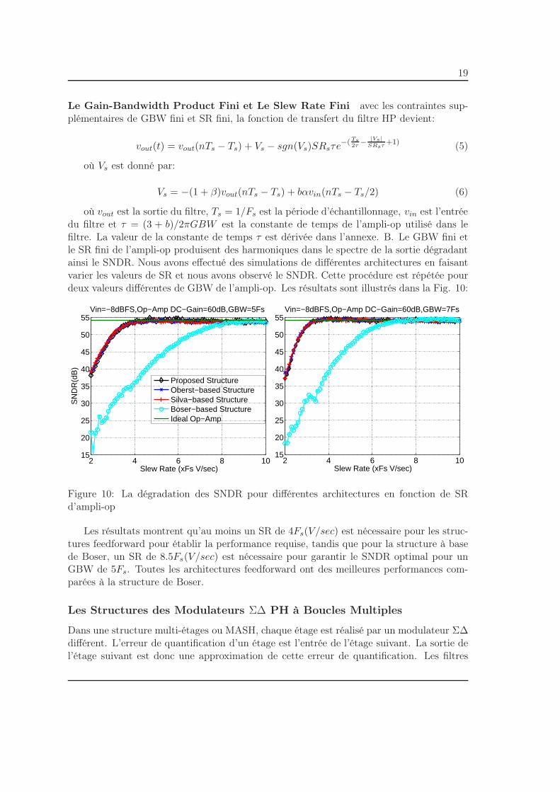
Le Gain-Bandwidth Product Fini et Le Slew Rate Fini avec les contraintes sup-plémentaires de GBW fini et SR fini, la fonction de transfert du filtre HP devient:
vout(t) = vout(nTs − Ts) + Vs − sgn(Vs)SRsτe−(Ts2τ
−|Vs|
SRsτ+1) (5)
où Vs est donné par:
Vs = −(1 + β)vout(nTs − Ts) + bαvin(nTs − Ts/2) (6)
où vout est la sortie du filtre, Ts = 1/Fs est la période d’échantillonnage, vin est l’entréedu filtre et τ = (3 + b)/2πGBW est la constante de temps de l’ampli-op utilisé dans lefiltre. La valeur de la constante de temps τ est dérivée dans l’annexe. B. Le GBW fini etle SR fini de l’ampli-op produisent des harmoniques dans le spectre de la sortie dégradantainsi le SNDR. Nous avons effectué des simulations de différentes architectures en faisantvarier les valeurs de SR et nous avons observé le SNDR. Cette procédure est répétée pourdeux valeurs différentes de GBW de l’ampli-op. Les résultats sont illustrés dans la Fig. 10:
2 4 6 8 1015
20
25
30
35
40
45
50
55
Slew Rate (xFs V/sec)
SN
DR
(dB
)
Vin=−8dBFS,Op−Amp DC−Gain=60dB,GBW=5Fs
2 4 6 8 1015
20
25
30
35
40
45
50
55
Slew Rate (xFs V/sec)
Proposed StructureOberst−based StructureSilva−based StructureBoser−based StructureIdeal Op−Amp
Vin=−8dBFS,Op−Amp DC−Gain=60dB,GBW=7Fs
Figure 10: La dégradation des SNDR pour différentes architectures en fonction de SRd’ampli-op
Les résultats montrent qu’au moins un SR de 4Fs(V/sec) est nécessaire pour les struc-tures feedforward pour établir la performance requise, tandis que pour la structure à basede Boser, un SR de 8.5Fs(V/sec) est nécessaire pour garantir le SNDR optimal pour unGBW de 5Fs. Toutes les architectures feedforward ont des meilleures performances com-parées à la structure de Boser.
Les Structures des Modulateurs Σ∆ PH à Boucles Multiples
Dans une structure multi-étages ou MASH, chaque étage est réalisé par un modulateur Σ∆différent. L’erreur de quantification d’un étage est l’entrée de l’étage suivant. La sortie del’étage suivant est donc une approximation de cette erreur de quantification. Les filtres
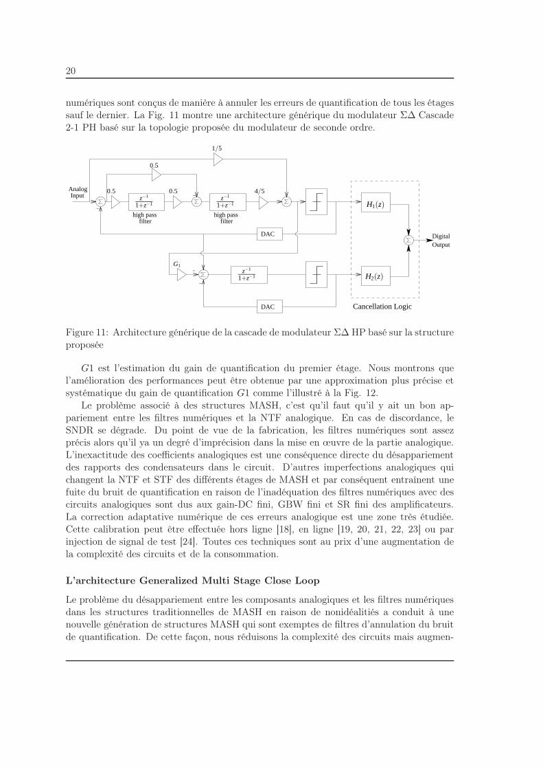
20
numériques sont conçus de manière à annuler les erreurs de quantification de tous les étagessauf le dernier. La Fig. 11 montre une architecture générique du modulateur Σ∆ Cascade2-1 PH basé sur la topologie proposée du modulateur de seconde ordre.
−
AnalogInput
high passfilter
−
filterhigh pass
DAC
DAC
−
−
Cancellation Logic
OutputDigital
0.5
1/5
z−1
1+z−1z−1
1+z−1 H1(z)
0.5 0.5 4/5
G1
H2(z)z−1
1+z−1
Figure 11: Architecture générique de la cascade de modulateur Σ∆ HP basé sur la structureproposée
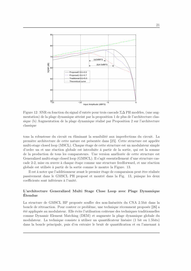
G1 est l’estimation du gain de quantification du premier étage. Nous montrons quel’amélioration des performances peut être obtenue par une approximation plus précise etsystématique du gain de quantification G1 comme l’illustré à la Fig. 12.
Le problème associé à des structures MASH, c’est qu’il faut qu’il y ait un bon ap-pariement entre les filtres numériques et la NTF analogique. En cas de discordance, leSNDR se dégrade. Du point de vue de la fabrication, les filtres numériques sont assezprécis alors qu’il ya un degré d’imprécision dans la mise en œuvre de la partie analogique.L’inexactitude des coefficients analogiques est une conséquence directe du désappariementdes rapports des condensateurs dans le circuit. D’autres imperfections analogiques quichangent la NTF et STF des différents étages de MASH et par conséquent entraînent unefuite du bruit de quantification en raison de l’inadéquation des filtres numériques avec descircuits analogiques sont dus aux gain-DC fini, GBW fini et SR fini des amplificateurs.La correction adaptative numérique de ces erreurs analogique est une zone très étudiée.Cette calibration peut être effectuée hors ligne [18], en ligne [19, 20, 21, 22, 23] ou parinjection de signal de test [24]. Toutes ces techniques sont au prix d’une augmentation dela complexité des circuits et de la consommation.
L’architecture Generalized Multi Stage Close Loop
Le problème du désappariement entre les composants analogiques et les filtres numériquesdans les structures traditionnelles de MASH en raison de nonidéalitiés a conduit à unenouvelle génération de structures MASH qui sont exemptes de filtres d’annulation du bruitde quantification. De cette façon, nous réduisons la complexité des circuits mais augmen-
21
−15 −10 −5 030
40
50
60
70
80
90
Input Amplitude (dBFS)
SQ
NR
(dB
)
Proposal2:G1=3.0
Proposal1:G1=3.7
Traditional:G1=5.0
Theoretical curve
(b)4.5dBFS
(a)3dBFS
Figure 12: SNR en fonction du signal d’entrée pour trois cascade Σ∆ PH modèles, (une aug-mentation) de la plage dynamique atteint par la proposition 1 de plus de l’architecture clas-sique (b) Augmentation de la plage dynamique réalisé par Proposition 2 sur l’architectureclassique
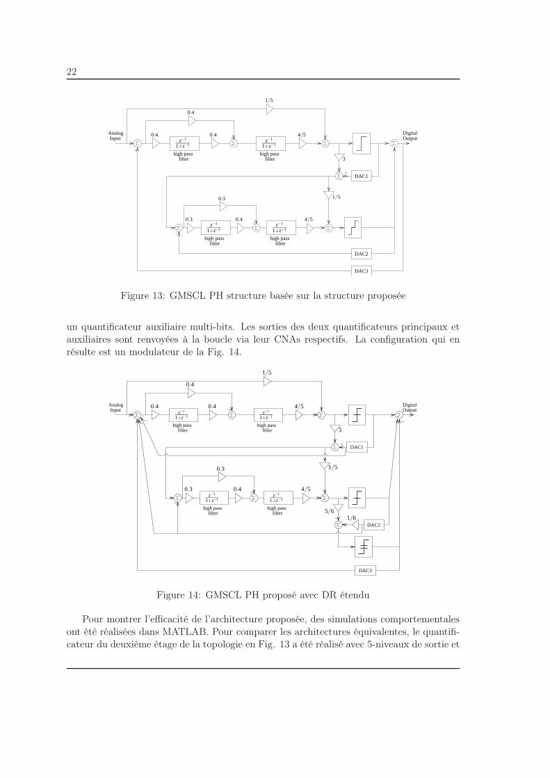
tons la robustesse du circuit en éliminant la sensibilité aux imperfections du circuit. Lapremière architecture de cette nature est présentée dans [25]. Cette structure est appeléemulti-stage closed loop (MSCL). Chaque étage de cette structure est un modulateur simpled’ordre un et une réaction globale est introduite à partir de la sortie, qui est la sommede la production de tous les comparateurs. Une version améliorée de cette structure estGeneralized multi-stage closed loop (GMSCL). Il s’agit essentiellement d’une structure cas-cade 2-2, mise en œuvre à chaque étape comme une structure feedforward, et une réactionglobale est utilisée à partir de la sortie comme le montre la Figure. 13.
Il est à noter que l’additionneur avant le premier étage de comparaison peut être réaliséepassivement dans le GMSCL PH proposé et montré dans la Fig. 13, puisque les deuxcoefficients sont inférieurs à l’unité.
L’architecture Generalized Multi Stage Close Loop avec Plage DynamiqueÉtendue
La structure de GMSCL HP proposée souffre des non-linéarités du CNA 2.5bit dans laboucle de rétroaction. Pour contrer ce problème, une technique récemment proposée [26] aété appliquée au modulateur. Elle évite l’utilisation coûteuse des techniques traditionnellescomme Dynamic Element Matching (DEM) et augmente la plage dynamique globale dumodulateur. La technique consiste à utiliser un quantificateur linéaire (1 bit ou 1.5bits)dans la boucle principale, puis d’en extraire le bruit de quantification et en l’amenant à
22
−high pass
filter
−
filterhigh pass
−
DigitalOutput
DAC1
DAC2
DAC3
AnalogInput
high passfilter
high passfilter
−
−
4/5z−1
1+z−1z−1
1+z−1
1/5
z−1
1+z−1z−1
1+z−1
3
1/5
4/50.4 0.4
0.4
0.3 0.4
0.3
Figure 13: GMSCL PH structure basée sur la structure proposée
un quantificateur auxiliaire multi-bits. Les sorties des deux quantificateurs principaux etauxiliaires sont renvoyées à la boucle via leur CNAs respectifs. La configuration qui enrésulte est un modulateur de la Fig. 14.
DAC3
DAC2
−high pass
filter
−
filterhigh pass
−DAC1
AnalogInput
high passfilter
high passfilter
−
−
OutputDigital
−−−
1/5
4/5z−1
1+z−1z−1
1+z−1
1/5
z−1
1+z−1z−1
1+z−1
3
4/50.4 0.4
0.4
0.3 0.4
0.3
1/65/6
Figure 14: GMSCL PH proposé avec DR étendu
Pour montrer l’efficacité de l’architecture proposée, des simulations comportementalesont été réalisées dans MATLAB. Pour comparer les architectures équivalentes, le quantifi-cateur du deuxième étage de la topologie en Fig. 13 a été réalisé avec 5-niveaux de sortie et

23
il utilise quatre comparateurs. L’architecture proposée (Fig. 14) a un comparateur et unquantificateur auxiliaire 4-niveaux dans la deuxième étape et donc quatre comparateurs.La modélisation des non-linéarités du CNA de moyenne 0 et de variance 1% a été introduitedans ces deux structures. Le résultat de la simulation présentée à la Fig. 15 montre que lastructure proposée fournie une performance 7dB meilleure que l’architecture traditionnelledu point de vue du SNR et 4dB d’amélioration de la performance du point de vue de laDR.
−60 −50 −40 −30 −20 −10 0 1010
20
30
40
50
60
70
80
90
100
110
Input Amplitude (dBFS)
SN
DR
(dB
)
Proposed
Traditional7dB
Figure 15: Comparaison des performances de deux structures GMSCL PH avec 1% non-linéarités du CNA
L’implémentation du Filtre Passe-Haut
Le filtre passe-haut est une composante majeure de modulateur Σ∆ PH. La fonction detransfert pour le filtre PH est réalisé en appliquant la transformation, z → −z, à unintégrateur basé sur un circuit à capacités commutées:
Hpasse−bas(z) =z−1
1 − z−1(7)
Il en résulte:
HPH(z) =−z−1
1 + z−1(8)

24
Ce filtre a un zéro à DC par opposition à un zéro à Fs/2 pour l’intégrateur à capacitéscommutées. Il y a trois filtres PH dans l’état de l’art: filtre à base d’intégrateur, filtre àbase de chopper et filtre amélioré.
Le Filtre à Base d’Intégrateur
La première mise en œuvre du filtre PH illustrée dans la Fig. 16 a été présenté dans [27]pour l’implémentation du modulateur Σ∆ passe-bande.
−
+
+
−
input+
input−
Td
Td
Sd
Sd
T
T
S
ST
T
Sd
Sd
S
S
Td
Td
C1A
C1B
C3A
C2A
C2B
C3B
out put−
out put+
Figure 16: Filtre PH faite par une boucle de rétroaction autour de l’intégrateur
Il est conçu par l’introduction d’une boucle supplémentaire de feed-back autour del’intégrateur, de telle sorte que la fonction de transfert pour le filtre HP est réalisé. Lesproblèmes associés à cette mise en œuvre comprennent une sensibilité accrue au bruit desampli-op [28], une haute contribution du bruit thermique des interrupteurs, une grandesuperficie et une consommation d’énergie élevée.
Le Filtre à Base de Chopper
La deuxième implémentation montrée dans la Fig. 17, est basée sur l’approche de lamodulation du signal d’entrée pour le ramener en bande de base, puis le signal est intégrépar l’intégrateur, et ensuite modulé pour remonter à la fréquence IF.
Toutefois, le traitement du signal se produit encore en bande de base au sein del’intégrateur. Les avantages obtenus par le déplacement à IF sont perdues une fois que lesignal est modulé vers la bande de base dans le domaine analogique, réintroduisant la né-cessité d’utiliser les techniques dites de “chopper stabilization (SHC)” et “correlated doublesampling (CDS)”.
25
−
+
+
−
(a)
(b)
input+
input−
S
STd
Td
Sd
T
T
ChopB
ChopB
ChopB
ChopB
out put−
out put+
C1A
C1B
Sd
ChopA ChopAC2B
ChopA ChopAC2A
S
T
ChopA
ChopB
Figure 17: (a) Filtre PH fait en hachant l’entrée et la sortie du signal d’intégrateur, (b)Son chronogramme associé
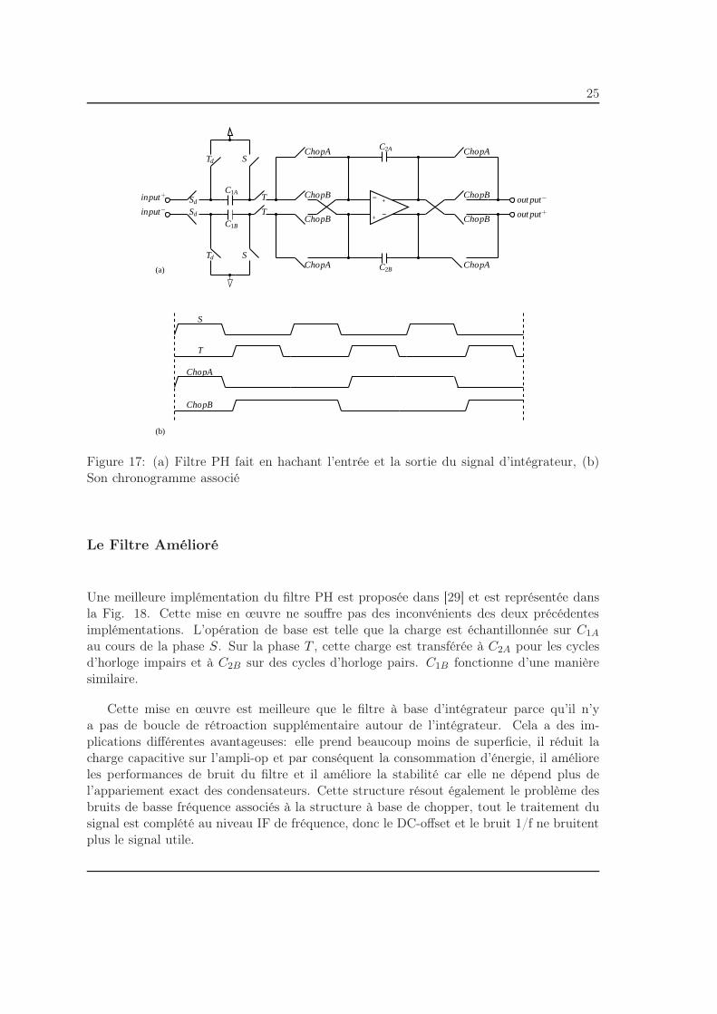
Le Filtre Amélioré
Une meilleure implémentation du filtre PH est proposée dans [29] et est représentée dansla Fig. 18. Cette mise en œuvre ne souffre pas des inconvénients des deux précédentesimplémentations. L’opération de base est telle que la charge est échantillonnée sur C1A
au cours de la phase S. Sur la phase T , cette charge est transférée à C2A pour les cyclesd’horloge impairs et à C2B sur des cycles d’horloge pairs. C1B fonctionne d’une manièresimilaire.
Cette mise en œuvre est meilleure que le filtre à base d’intégrateur parce qu’il n’ya pas de boucle de rétroaction supplémentaire autour de l’intégrateur. Cela a des im-plications différentes avantageuses: elle prend beaucoup moins de superficie, il réduit lacharge capacitive sur l’ampli-op et par conséquent la consommation d’énergie, il amélioreles performances de bruit du filtre et il améliore la stabilité car elle ne dépend plus del’appariement exact des condensateurs. Cette structure résout également le problème desbruits de basse fréquence associés à la structure à base de chopper, tout le traitement dusignal est complété au niveau IF de fréquence, donc le DC-offset et le bruit 1/f ne bruitentplus le signal utile.

26
−
+
+
−
(a)
(b)
T
ChopA
ChopB
SC
hopATd
Td
Sd
Sd
T
T
S
S
C1A
C1B
C2A
C2B
out put−
out put+
input+
input−
Cho
pBC
hopB
Cho
pA
Cho
pAC
hopA
Cho
pB
Cho
pB
Figure 18: (a) Filtre PH amélioré, (b) Son chronogramme associé
La Comparaison Analytique
Les trois implémentations de filtre PH sont comparées théoriquement du point de vue deleur immunité contre le bruit du commutateur, le bruit d’ampli-op, les capacités parasiteset non-idéalités d’ampli-op soit finie DC-gain, finie GBW et SR. Cette analyse est présentéede façon concise dans le Tableau. 1.
Ces résultats prouvent que le filtre PH amélioré est le meilleur parmi les trois implé-mentations. Non seulement il est à l’abri du bruit de scintillement et DC-offsets, il offreégalement la résistance maximum contre les bruits de commutateur, le bruit d’ampli-op etces non-idéalités.
La Comparaison Pratique
L’analyse comparative analytique est prouvée par la simulation des circuits avec le simula-teur électrique: SPECTRE de Cadence. A cet effet, les modèles-macros des blocs de basesont utilisés. Dans la première expérience, on mesure le SNDR du modulateur en faisantvarier la fréquence d’échantillonnage pour chaque type de filtre tout en gardant l’ampli-opGBW constant.
Le résultat se reflète dans la Fig. 19:Cela montre que le filtre à base de chopper et le filtre amélioré peuvent fonctionner à
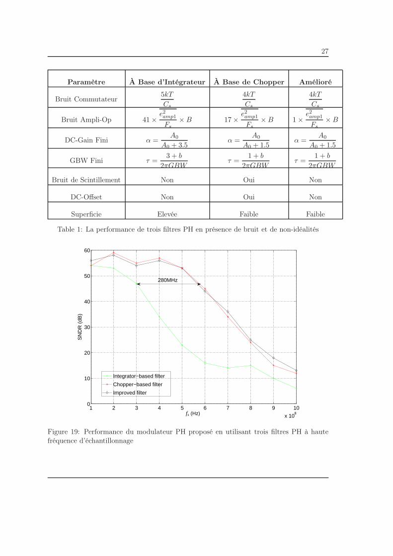
27
Paramètre À Base d’Intégrateur À Base de Chopper Amélioré
Bruit Commutateur5kT
Cs
4kT
Cs
4kT
Cs
Bruit Ampli-Op 41 ×e2amp1
Fs× B 17 ×
e2amp1
Fs× B 1 ×
e2amp1
Fs× B
DC-Gain Fini α =A0
A0 + 3.5α =
A0
A0 + 1.5α =
A0
A0 + 1.5
GBW Fini τ =3 + b
2πGBWτ =
1 + b
2πGBWτ =
1 + b
2πGBW
Bruit de Scintillement Non Oui Non
DC-Offset Non Oui Non
Superficie Elevée Faible Faible
Table 1: La performance de trois filtres PH en présence de bruit et de non-idéalités
1 2 3 4 5 6 7 8 9 10
x 108
0
10
20
30
40
50
60
SN
DR
(dB
)
Improved filter
Integrator−based filter
Chopper−based filter
280MHz
fs (Hz)
Figure 19: Performance du modulateur PH proposé en utilisant trois filtres PH à hautefréquence d’échantillonnage

28
une fréquence d’échantillonnage qui est supérieure à 280MHz par rapport à la fréquenced’échantillonnage la plus élevées possible pour le filtre à base d’intégrateur en utilisant lamême ampli-op. En d’autres termes, à la même consommation d’énergie, le modulateurréalisé avec un filtre à base d’intégrateur peut convertir moins de bande passante que lemodulateur construit avec les deux autres topologies de filtre.
Dans la deuxième expérience, nous prouvons la réjection excellente du bruit obtenupar le filtre amélioré par rapport aux deux autres topologies. Le bruit de l’amplificateuropérationnel ramené à l’entrée a été généré en MATLAB. Il est injecté dans le circuit enajoutant une source de tension à chaque entrée de l’ampli-op. Les valeurs de cette sourcede tension sont lues à partir de MATLAB. Le circuit pour le modulateur PH proposé,construit avec la topologie de filtre amélioré, y compris les sources de bruit de l’ampli-opest illustré dans la Fig. 20.
−
+
+
−
−
+
+
−
DAC
ChopBChopAChopA
ChopB ChopA ChopA ChopBTd
Td
Sd
Sd
S
S
T
T
ChopB
Sd
Sd
Td
Td
C5
C5
T
T
input−V re f−
ChopB
ChopB ChopBChopAChopA
ChopA ChopA ChopBTd
C4
C4
Sd
Sd
T
SS
Td
T
V re f−
V re f +
Digitalout put
input+
input−
Td
Td
Sd
Sd
S
S
V re f +
V re f−
C2A
C2B
C1A
C1B
e+amp
e−amp
C1A
C1B
Td Sd
C1A
SdTd
input+V re f +
C1B
C2A
C2B
Figure 20: Injection de bruit dans le modulateur
e+amp et e−amp sont les sources de bruit généré en MATLAB et lu directement dans
SPECTRE. Le résultat de la simulation de l’injection du bruit dans les trois filtres estindiqué sur la Fig. 21.
Cette figure montre que le filtre à base d’intégrateur et le filtre amélioré réussissent àéviter le bruit de basse fréquence-bruit de scintillement, tandis que dans le filtre à base dechopper, le bruit de scintillement corrompt la bande du signal et en résulte la réductionde la SNR. Pour un OSR de 32, le filtre à base d’intégrateur, le filtre à base de chopperet le filtre amélioré donnent une SNDR de 55dB, 52dB et 21dB respectivement. Ainsi,3dB de SNR est perdu à cause de la désavantageuse mise en forme du bruit d’ampli-opà haute fréquence dans la structure à base d’intégrateur et 30dB sont gaspillées en raisonde la corruption du signal utile par le bruit à basse fréquence dans la structure à base dechopper. Ces caractéristiques font du filtre amélioré un choix idéal pour la grande vitesseet haute résolution à consommation réduite.

29
10−4
10−3
10−2
10−1
−100
−90
−80
−70
−60
−50
−40
−30
−20
−10
0
integrator−based filter
Frequency (xFs Hz)
PS
D (
dB/H
z)improved filter
chopper−based filter
Figure 21: Spectre de sortie de modulateur en présence de bruit d’ampli-op pour les troisfiltres
La Conception en 65nm CMOS
Le CAN développé au niveau système dans les chapitres précédents a été conçu au niveautransistor en CMOS 65nm. Ce CAN est conçu pour satisfaire les exigences de performancedes normes spécifiées dans le Tableau. :
Au vu de la diversité des exigences de performance, il devient évident que le CANdoit être reconfigurable. La reconfiguration est fournie par le changement de la fréquenced’échantillonnage (Fs) et de l’ordre du modulateur (M). Dans le mode GSM/EDGE,puisque la bande passante du signal est faible, une Fs de 28.57MHz (OSR = 28.57MHz
2×135KHz ≈105) et une mise en forme du 2ème ordre du bruit avec un seul bit de quantificationsont utilisés. Ainsi, le deuxième étage de la structure GMSCL PH est désactivée dansle mode GSM/EDGE pour réduire la consommation. Pour le mode de fonctionnementUMTS/WLAN , la fréquence d’échantillonnage est élevée à 228.57MHz et l’ordre du mod-ulateur est porté à 4, avec un étage supplémentaire de quantificateur auxiliaire.
Le Schéma Global du Circuit
Le schéma du modulateur en mode GSM est présenté dans sa version non différentielle pourplus de simplicité dans la Fig. 22. Le commutateur d’entrée du modulateur est de type“bootstrap” pour satisfaire les exigences de linéarité. Les autres commutateurs sont descommutateurs CMOS. La capacité d’échantillonnage à l’entrée du modulateur est choisie

30
Standard GSM/EDGE UMTS WLAN
Taux de conversion 270KHz 3.84MHz 25MHz
Bande passante du signal 135kHz 1.92MHz 12.5MHz
Fréquence d’échantillonnage (Fs) 28.57MHz 228.57MHz 228.57MHz
Ordre du Modulateur (P ) 2 4+aux. quantizer 4+aux. quantizer
SNR 80dB 80dB 52dB
Table 2: ADC Spécification
égale à 600fF pour répondre aux spécifications de bruit thermique.
−1
−1
−1
−1
+
−
+
− +
−
−1
Td
Sd
T
S
A
B
Sd
Td
1.125p
Sd
S
Sd
1.5p
Sd
V re f n1
inputOTA1
OTA2
Sd
T
Td S
T
Td
A B A B
A B A B
100f
600f450f
400f
T
45
0f
out put
T d
V re f p1
Figure 22: Modulateur global non différentiel en mode GSM avec son chronogramme as-socié
Le modulateur utilisé est du 2ème ordre avec l’architecture proposée et un quantifica-teur 1 bit. Ce modulateur fournit les performances nécessaires de SNDR pour un OSR de84. La taille des condensateurs diminue avec le flux de signal en raison de l’augmentationde la mise en forme du bruit.
Le schéma du modulateur non différentiel en mode ULAN est présenté sur la Fig. 23.Il utilise la structure proposée-GMSCL PH avec une dynamique améliorée par l’ajout d’unquantificateur auxiliaire dans le dernier étage comme décrit précédemment.
La mise en œuvre au niveau transistor d’un CAN multi-mode fonctionnant sur leprincipe du modulation Σ∆ passe-haut est présenté. Le CAN a deux modes de fonc-

31
−1
−1
−1
−1
−
1
−1
−1
−1
+
−
+
− +
−
+
− +
−
+
−
+
−
−1
−1
100f
S
T d
100f
100f
Td
Td
100f
Sd
Td
1.125p
Sd
S
Sd
1.5p
Sd
inputOTA1
OTA2
Sd
T
Td S
T
Td
A B A B
A B A B
100f
600f450f
400f
Sd
Td
300f
OTA4
S
T
A B A B400f
200f
100f
100fSd
Sd
Sd
OTA3T
A B A B
300f
Sd
Sd
Sd
Sd
200f
Sd
50f
Sd
200f
Sd
Sd
Y1
Td
45
0f
Sd
Td
Y2 Σ
2b
Y3
Sd
Sd
Td
T d,Y2
V re f n1
V re f p1
V re f p1
V re f n1
V re f p1V re f p2V re f p3V re f p4V re f n4V re f n3V re f n2V re f n1
V re f n1
V re f p1
V re f p1
V re f n1
V re f n1
V re f p1
Vco
mp1
Vco
mp2
Vco
mp3
Td,Y
Td,Y1
V re f n1
V re f p1
Td,Y1
Td,Y2
Y
Td,−Y1
Td,−Y2
T d T d T d
50f50f50f
Figure 23: Modulateur global non différentiel en mode UMTS/WLAN
tionnement: GSM/EDGE et UMTS/WLAN. Cette reconfiguration permet une économied’énergie significative.
Les Résultats de Simulations
La simulation électrique avec des OTA (et le circuit CMFB), quantificateur et CNA im-plementés au niveau transistor est effectuée avec succès pour le mode GSM. Le spectrede sortie à l’entrée pleine échelle est illustré dans la Fig. 24. Comme présenté dans lafigure, la résolution de 80-dB est atteinte à l’OSR minimum de 84 et de la fréquenced’échantillonnage de 28.57MHz.
Pour les modes UMTS/WiFi de fonctionnement, une distorsion importante est observéedans la bande du signal. Le résultat de la simulation propre de ces modes est prévu dansune extension éventuelle de ce travail de recherche.

32
10−4
10−3
10−2
10−1
100
−100
−80
−60
−40
−20
0
20
Frequency (xFs Hz)
PS
D (
dB/H
z)
Fs=28.57MHz,Fin=14.18MHz,OSR=84,SNDR=80dB
fb
Figure 24: Résultat de simulation en mode GSM
Conclusion
La première partie de cette thèse a présenté les architectures de récepteur radio pourles systèmes de communication sans fil d’aujourd’hui du point de vue de la reconfigura-tion, intégrabilité et consommation d’énergie. Un pas en avant important vers la miseen œuvre de la notion de SDR sont les récepteurs d’échantillonnage RF qui utilisent lesous-échantillonnage pour réduire la fréquence de signal de RF à IF. De cette façon, letraitement du signal en temps discret, qui est fortement intégrable, est introduit dès ledébut. En utilisant le sous-échantillonnage, les exigences de vitesse sur les blocs suivantssont assouplies. Le défi dans ce scénario est le filtrage anti-repliements pour minimiser lacorruption du signal par des brouilleurs en-bande et hors-bande. Ceci est accompli par desfiltres à capacités commutées passifs. L’état de l’art des récepteurs utilise une downcon-version en deux étapes, chaque étape à l’aide de sous-échantillonnage, afin de parvenir àun compromis acceptable entre la fréquence du signal abaissée en fréquence et le filtrageanti-repliement. Bien que, avec l’augmentation des performances des CAN, il est devenupossible d’utiliser la “downconversion” en une seule étape pour diminuer le nombre decomposants. Le sous-échantillonnage est réalisé de telle manière que le signal est placé àFs/2 pour profiter des avantages des deux: zéro-IF et low-IF. Dans ce scénario, le candidatnaturel pour le CAN est le modulateur Σ∆ PH.
La deuxième partie de cette thèse a examiné l’état de l’art des modulateurs Σ∆. Com-mençant par des architectures classiques feed-back, ensuite les récentes architectures feed-forward sont discutés avec leurs avantages et leur inconvénients. Les modulateurs d’ordresupérieur à boucle unique et modulateurs en plusieurs étages, qui sont inévitables pour desapplications nécessitant une haute résolution, sont également exposés. La modélisation au
33
niveau du système du modulateur classique: Boser second ordre [12] est effectuée afin dedémontrer les exigences relatives pour les ampli-op dans cette topologie.
La troisième partie est liée à l’étude du modulateur Σ∆ PH. Ce dernier rejette le bruitde quantification en basse fréquence. La bande du signal est située à environ la moitié dela fréquence d’échantillonnage, il est donc compatible avec le récepteur Fs/2 IF en tempsdiscret et, en outre, totalement à l’abri des DC-offsets et du bruit de scintillement. Diversestopologies existantes de modulateur Σ∆ passe-bas sont présentées après leur adaptation aufonctionnement PH, et une nouvelle architecture du second ordre ayant une STF unitaireest proposée. Elle soulage les problèmes liés à l’architecture traditionnelle feedforward ensupprimant la nécessité d’un additionneur actif. Une nouvelle technique pour concevoirdes structures en cascade ou MASH est également proposée ce qui augmente la dynamiqueen entrée du modulateur. Cette technique est basée sur l’étude systématique du gain dequantification du premier étage et l’adaptation de filtres numériques avec ce gain. Unétat de l’art des architectures des modulateurs Σ∆ multi-étages, ce qui est libre de fil-tres numériques d’annulation, appelé Generalized-Multi-Stage-Closed-Loop (GMSCL) estconçu pour un fonctionnement PH. Enfin, un quantificateur auxiliaire est ajouté dans ledeuxième étage, afin d’augmenter la gamme dynamique en entrée et de diminuer l’effetdes non-linéarités du CAN global. Une comparaison entre les modulateurs Σ∆ PH etpasse-bas est également réalisée. Elle révèle que les modulateurs PH sont plus sensibles àla gigue d’horloge ce qui augmente les contraintes sur le circuit de génération d’horloge.Les modulateurs passe-bas d’autre part sont de plus en plus sensibles à l’hystérésis dansle comparateur nécessitant un plan pour réduire les exigences sur le comparateur.
La quatrième partie de ce travail de recherche visait à sélectionner la meilleure archi-tecture du filtre PH qui est l’élément de base de modulateur Σ∆ PH. Après une analysecomparative approfondie des trois topologies en compétition, celle qui a été introduiterécemment et basée sur l’alternance des condensateurs est sélectionnée. Ses avantages deréduction de la consommation et du bruit sont prouvés analytiquement et par simulations.
Enfin, une implementation multi-standard, multi-mode d’un CAN en CMOS 65nm estprésentée. Il a trois modes de fonctionnement: GSM, UMTS et WiFi/WiMax. En modeGSM, le modulateur Σ∆ PH de second ordre proposé est utilisé, tandis que pour l’UMTSet le WiFi/WiMax le modulateur GMSCL PH du quatrième ordre avec un quantificateurauxiliaire est utilisé pour la conversion.

34
35
Contents
1 Introduction 391.1 Motivation and Goals . . . . . . . . . . . . . . . . . . . . . . . . . . . . . . 391.2 Organization . . . . . . . . . . . . . . . . . . . . . . . . . . . . . . . . . . . 40
2 RF Receiver Architecture 432.1 Introduction . . . . . . . . . . . . . . . . . . . . . . . . . . . . . . . . . . . . 432.2 Superheterodyne Receiver . . . . . . . . . . . . . . . . . . . . . . . . . . . . 442.3 Digital-IF Receiver . . . . . . . . . . . . . . . . . . . . . . . . . . . . . . . . 452.4 Direct Conversion Receiver . . . . . . . . . . . . . . . . . . . . . . . . . . . 462.5 Low-IF Receiver . . . . . . . . . . . . . . . . . . . . . . . . . . . . . . . . . 482.6 Bandpass Sampling Receiver . . . . . . . . . . . . . . . . . . . . . . . . . . . 49
2.6.1 Theory of bandpass sampling . . . . . . . . . . . . . . . . . . . . . . 502.6.2 Drawback of subsampling - Noise spectrum aliasing . . . . . . . . . . 512.6.3 Bandpass Receiver Configuration . . . . . . . . . . . . . . . . . . . . 532.6.4 Fs/2 IF Bandpass-Sampling Receiver . . . . . . . . . . . . . . . . . . 55
2.6.4.1 RF Stage . . . . . . . . . . . . . . . . . . . . . . . . . . . . 572.6.4.2 First DTASP Stage . . . . . . . . . . . . . . . . . . . . . . 572.6.4.3 Second DTASP Stage . . . . . . . . . . . . . . . . . . . . . 582.6.4.4 Frequency Plans . . . . . . . . . . . . . . . . . . . . . . . . 592.6.4.5 Proposed Frequency Plans . . . . . . . . . . . . . . . . . . 60
2.7 Conclusion . . . . . . . . . . . . . . . . . . . . . . . . . . . . . . . . . . . . . 61
3 ∆Σ Modulator and System Level Modeling 633.1 Introduction . . . . . . . . . . . . . . . . . . . . . . . . . . . . . . . . . . . . 633.2 Working Principle . . . . . . . . . . . . . . . . . . . . . . . . . . . . . . . . 64
3.2.1 Stability . . . . . . . . . . . . . . . . . . . . . . . . . . . . . . . . . . 673.3 Second-Order ∆Σ Modulator Architectures . . . . . . . . . . . . . . . . . . 68
3.3.1 Boser Structure . . . . . . . . . . . . . . . . . . . . . . . . . . . . . . 683.3.1.1 Linear Analysis . . . . . . . . . . . . . . . . . . . . . . . . . 693.3.1.2 Disadvantage of Boser Structure . . . . . . . . . . . . . . . 70
3.3.2 Silva Structure . . . . . . . . . . . . . . . . . . . . . . . . . . . . . . 703.3.2.1 Linear Analysis . . . . . . . . . . . . . . . . . . . . . . . . . 713.3.2.2 Disadvantages of Silva Structure . . . . . . . . . . . . . . . 71

36 CONTENTS
3.3.3 Oberst Structure . . . . . . . . . . . . . . . . . . . . . . . . . . . . . 713.3.3.1 Linear Analysis . . . . . . . . . . . . . . . . . . . . . . . . . 723.3.3.2 Disadvantages of Oberst Structure . . . . . . . . . . . . . . 72
3.4 Higher-Order ∆Σ Modulator Architectures . . . . . . . . . . . . . . . . . . . 733.4.1 Single-Loop Higher-Order . . . . . . . . . . . . . . . . . . . . . . . . 73
3.4.1.1 Cascade of integrators with distributed feedback (CIFB)structure . . . . . . . . . . . . . . . . . . . . . . . . . . . . 74
3.4.1.2 Cascade of resonators with distributed feedback (CRFB)structure . . . . . . . . . . . . . . . . . . . . . . . . . . . . 75
3.4.1.3 Cascade of integrators with distributed feedforward (CIFF)structure . . . . . . . . . . . . . . . . . . . . . . . . . . . . 75
3.4.1.4 Cascade of resonators with distributed feedforward (CRFF)structure . . . . . . . . . . . . . . . . . . . . . . . . . . . . 76
3.4.2 Multi-Stage Modulators . . . . . . . . . . . . . . . . . . . . . . . . . 763.4.3 Classic Cascade 2-1 MASH Structure . . . . . . . . . . . . . . . . . . 77
3.4.3.1 Linear Analysis . . . . . . . . . . . . . . . . . . . . . . . . . 783.4.4 Advanced MASH Structures . . . . . . . . . . . . . . . . . . . . . . . 79
3.5 Multibit Modulators . . . . . . . . . . . . . . . . . . . . . . . . . . . . . . . 803.6 Continuous Time and Hybrid (Continuous Time/Discrete Time) Modulators 823.7 System Level Modeling . . . . . . . . . . . . . . . . . . . . . . . . . . . . . . 84
3.7.1 Clock Jitter . . . . . . . . . . . . . . . . . . . . . . . . . . . . . . . . 853.7.2 Switch and Op-Amp Noise . . . . . . . . . . . . . . . . . . . . . . . . 85
3.7.2.1 Switch Thermal Noise . . . . . . . . . . . . . . . . . . . . . 853.7.2.2 Op-amp Noise . . . . . . . . . . . . . . . . . . . . . . . . . 87
3.7.3 Op-amp Non-Idealities . . . . . . . . . . . . . . . . . . . . . . . . . . 873.7.3.1 Saturation . . . . . . . . . . . . . . . . . . . . . . . . . . . 873.7.3.2 Finite DC-Gain . . . . . . . . . . . . . . . . . . . . . . . . 893.7.3.3 Finite Gain-Bandwidth Product and Slew Rate . . . . . . . 91
3.7.4 Comparator Non-Idealities . . . . . . . . . . . . . . . . . . . . . . . . 933.8 Conclusion . . . . . . . . . . . . . . . . . . . . . . . . . . . . . . . . . . . . . 96
4 High-Pass ∆Σ Modulator 974.1 Introduction . . . . . . . . . . . . . . . . . . . . . . . . . . . . . . . . . . . . 974.2 Principle . . . . . . . . . . . . . . . . . . . . . . . . . . . . . . . . . . . . . . 974.3 Single-Loop HP ∆Σ Modulator Structures . . . . . . . . . . . . . . . . . . . 99
4.3.1 Boser-based Structure . . . . . . . . . . . . . . . . . . . . . . . . . . 994.3.2 Silva-based Structure . . . . . . . . . . . . . . . . . . . . . . . . . . . 1004.3.3 Oberst-based Structure . . . . . . . . . . . . . . . . . . . . . . . . . 1014.3.4 Proposed Unity-STF Structure . . . . . . . . . . . . . . . . . . . . . 101
4.3.4.1 Linear Analysis . . . . . . . . . . . . . . . . . . . . . . . . . 1014.3.4.2 Refining the Proposed Architecture . . . . . . . . . . . . . 102
4.4 Comparative Analysis of Single-Loop HP Modulators . . . . . . . . . . . . . 1054.4.1 High-Pass Filter Output Excursion . . . . . . . . . . . . . . . . . . . 1074.4.2 Op-Amp Non-Idealities Effect . . . . . . . . . . . . . . . . . . . . . . 110

37
4.4.2.1 Finite DC-Gain . . . . . . . . . . . . . . . . . . . . . . . . 1104.4.2.2 Finite Gain-Bandwidth Product and Slew Rate . . . . . . . 112
4.5 Multi-Stage HP ∆Σ Modulator Structures . . . . . . . . . . . . . . . . . . . 1134.5.1 Cascade 2-1 HP Delta Sigma Modulator Structure . . . . . . . . . . 1144.5.2 Quantizer Linear Model and Quantizer Gain Calculation . . . . . . . 1154.5.3 Quantization Noise Cancellation Filters’ Designing . . . . . . . . . . 116
4.5.3.1 Second-Stage Quantizer Gain G2 . . . . . . . . . . . . . . . 1174.5.3.2 First-Stage Quantizer Gain G1 . . . . . . . . . . . . . . . . 117
4.5.4 Generalized Multi Stage Close Loop . . . . . . . . . . . . . . . . . . 1214.5.5 Generalized Multi Stage Close Loop with Extended Dynamic Range 122
4.6 Conclusion . . . . . . . . . . . . . . . . . . . . . . . . . . . . . . . . . . . . . 125
5 High-Pass Filter Implementation 1295.1 Introduction . . . . . . . . . . . . . . . . . . . . . . . . . . . . . . . . . . . . 1295.2 Integrator-based Structure . . . . . . . . . . . . . . . . . . . . . . . . . . . . 130
5.2.1 Switch Noise . . . . . . . . . . . . . . . . . . . . . . . . . . . . . . . 1305.3 Op-Amp Noise . . . . . . . . . . . . . . . . . . . . . . . . . . . . . . . . . . 132
5.3.1 Parasitic Capacitances . . . . . . . . . . . . . . . . . . . . . . . . . . 1365.3.2 Op-Amp Non-Idealities . . . . . . . . . . . . . . . . . . . . . . . . . 138
5.3.2.1 Finite DC-Gain . . . . . . . . . . . . . . . . . . . . . . . . 1385.3.2.2 Finite Gain-Bandwidth Product and Slew Rate . . . . . . . 139
5.4 Chopper-based Structure . . . . . . . . . . . . . . . . . . . . . . . . . . . . . 1415.4.1 Switch Noise . . . . . . . . . . . . . . . . . . . . . . . . . . . . . . . 1415.4.2 Op-Amp Noise . . . . . . . . . . . . . . . . . . . . . . . . . . . . . . 1425.4.3 Parasitic Capacitances . . . . . . . . . . . . . . . . . . . . . . . . . . 1455.4.4 Op-Amp Non-Idealities . . . . . . . . . . . . . . . . . . . . . . . . . 146
5.4.4.1 Finite DC-Gain . . . . . . . . . . . . . . . . . . . . . . . . 1465.4.4.2 Finite Gain-Bandwidth Product and Slew Rate . . . . . . . 147
5.5 Improved Structure . . . . . . . . . . . . . . . . . . . . . . . . . . . . . . . . 1495.5.1 Switch Noise . . . . . . . . . . . . . . . . . . . . . . . . . . . . . . . 1505.5.2 Op-Amp Noise . . . . . . . . . . . . . . . . . . . . . . . . . . . . . . 1515.5.3 Parasitic Capacitances . . . . . . . . . . . . . . . . . . . . . . . . . . 1545.5.4 Op-Amp Non-Idealities . . . . . . . . . . . . . . . . . . . . . . . . . 155
5.5.4.1 Finite DC-Gain . . . . . . . . . . . . . . . . . . . . . . . . 1555.5.4.2 Finite Gain-Bandwidth Product and Slew Rate . . . . . . . 156
5.5.5 High Frequency Performance Analysis . . . . . . . . . . . . . . . . . 1585.5.6 Noise Analysis . . . . . . . . . . . . . . . . . . . . . . . . . . . . . . 159
5.5.6.1 Noise Generation . . . . . . . . . . . . . . . . . . . . . . . . 1605.5.6.2 Noise Injection in Circuit . . . . . . . . . . . . . . . . . . . 160
5.6 Comparative Analysis between Low-Pass and High-Pass ∆Σ Modulators . . 1615.6.1 Clipping . . . . . . . . . . . . . . . . . . . . . . . . . . . . . . . . . . 1625.6.2 Op-Amp DC-Gain . . . . . . . . . . . . . . . . . . . . . . . . . . . . 1625.6.3 Op-Amp GBW and SR . . . . . . . . . . . . . . . . . . . . . . . . . 1635.6.4 Clock Jitter . . . . . . . . . . . . . . . . . . . . . . . . . . . . . . . . 163

38 CONTENTS
5.6.5 Comparator Hysteresis . . . . . . . . . . . . . . . . . . . . . . . . . . 1645.7 Conclusion . . . . . . . . . . . . . . . . . . . . . . . . . . . . . . . . . . . . . 166
6 Design in 65nm CMOS 1676.1 Introduction . . . . . . . . . . . . . . . . . . . . . . . . . . . . . . . . . . . . 1676.2 System level specifications . . . . . . . . . . . . . . . . . . . . . . . . . . . . 1686.3 Global Circuit Schematic . . . . . . . . . . . . . . . . . . . . . . . . . . . . 1686.4 Passive Adder . . . . . . . . . . . . . . . . . . . . . . . . . . . . . . . . . . . 1706.5 Quantizer . . . . . . . . . . . . . . . . . . . . . . . . . . . . . . . . . . . . . 1746.6 DAC . . . . . . . . . . . . . . . . . . . . . . . . . . . . . . . . . . . . . . . . 1746.7 Simulation results . . . . . . . . . . . . . . . . . . . . . . . . . . . . . . . . . 1756.8 Conclusion . . . . . . . . . . . . . . . . . . . . . . . . . . . . . . . . . . . . . 177
7 Conclusion and Perspectives 1797.1 Summary . . . . . . . . . . . . . . . . . . . . . . . . . . . . . . . . . . . . . 1797.2 Perspectives . . . . . . . . . . . . . . . . . . . . . . . . . . . . . . . . . . . . 180
A Charge-Transfer Transient in Integrator 183A.0.1 Phase S,n . . . . . . . . . . . . . . . . . . . . . . . . . . . . . . . . . 184A.0.2 Phase T,n-1/2 . . . . . . . . . . . . . . . . . . . . . . . . . . . . . . 184
B Charge-Transfer Transient in Integrator-based HP Filter 187B.0.3 Phase S,n . . . . . . . . . . . . . . . . . . . . . . . . . . . . . . . . . 188B.0.4 Phase T,n-1/2 . . . . . . . . . . . . . . . . . . . . . . . . . . . . . . 188
C Charge-Transfer Transient in Chopper-based HP Filter 191C.0.5 Phase S,Chop A,n . . . . . . . . . . . . . . . . . . . . . . . . . . . . 191C.0.6 Phase T,Chop A,n-1/2 . . . . . . . . . . . . . . . . . . . . . . . . . . 191
D Charge-Transfer Transient in Improved HP Filter 195D.0.7 Phase S,A,n . . . . . . . . . . . . . . . . . . . . . . . . . . . . . . . . 195D.0.8 Phase T,Chop A,n-1/2 . . . . . . . . . . . . . . . . . . . . . . . . . . 195
Bibliography 208

39
Chapter 1
Introduction
1.1 Motivation and Goals
The proliferation of wireless standards and the diminution of radio-terminals’ size at thesame time is pushing towards the materialization of newly created concept of software de-fined radio (SDR). This communication system is expected to realise multiband, multimoderadio terminals by defining radio functionality in software [1]. This way, the radio terminalis adapted to different protocols and customized for diverse services by just reprogrammingthe radio functionality.
This, however, makes the RF-receiver design a challenging task. In an ideal SDR, thesolution for increasing both the receiver integration and reconfigurability is provided bytransferring the analog-to-digital-conversion interface from the baseband to RF i-e just afterthe antenna. The inherent advantage of this scheme is that the digital signal processingeliminates the non-idealities associated with analog signal processing i-e device noise andnon-linearities, components mismatch etc. The evolution of CMOS technologies towardssmaller transistor feature sizes also favours an increased level of digital signal processingin receiver implementation [2].
Nowadays the DSP can operate at a very high frequency and can thus process highfrequency signals. The boundary between the RF front-end and the digital baseband ismoved to higher frequency, but not yet at RF frequency. The major bottleneck is the designof analog-to-digital-converter (ADC) which can convert the signal at high frequencies.With the current CMOS technologies, it is practically not possible to design an ADCwhich converts the signal directly at RF.
However, the processing has to be carried out as much as possible in digital due tothe low costs, reconfigurability possibility and stability. To go forward in this direction,sub-sampling receiver was proposed. The RF signal is sub-sampled as soon as possible.The frequency downconversion is carried out by the sub-sampler with discrete-time signalprocessing. One special case of RF receiver which uses discrete-time subsampling is Fs/2IF receiver [3, 4]. This architecture downscales the frequency from RF to an IF of Fs/2(one-half of the sampling frequency), thereby making High-Pass (HP) ∆Σ modulator thenatural choice for ADC. This ADC is of much reduced complexity as compared to Band-

40 1. Introduction
Pass (BP) ∆Σ modulator.Besides the advantage of converting directly at IF, HP ∆Σ modulator has the poten-
tial to efficiently eliminate the dc-offsets and low-frequency noises like flicker noise [5, 6, 7]which are a source of concern in traditional LP ∆Σ modulators. This feature is particu-larly interesting for time-interleaved ∆Σ converters where the channel-offset is sufficientlyremoved by HP operation [8], and a simple digital channel equalization technique wouldminimize effectively the channel gain mismatch effect [30].
Inspite of these potential advantages, the concept of HP ∆Σ modulation has not re-ceived much attention, mostly due to its difficult implementation and the uncertainty aboutits stability and performance in the presence of circuit nonidealities. The basic hindranceblock has been the implementation of high pass filter, which is analogous to an integratorin LP ∆Σ modulator. The traditional implementation involves a feedback loop aroundan integrator and is an expensive solution because of increased power consumption andsurface area. However, recently a new architecture of HP filter has been proposed, whichgets rid of the drawbacks of the traditional one and hence propels a renewed interest inHP ∆Σ modulators.
Keeping in view its potentials, this thesis is focused on HP ∆Σ modulator in generaland its application to multi-mode wireless receivers in particular. Our objectives consistof studying its principle, its performance and stability and comparing it to LP modulatorson one hand and applying it to achieve multi-modal wireless receiver functionality on theother.
To achieve these objectives, a new unity signal-transfer-function (STF) single-loopHP ∆Σ modulator architecture has been proposed. It is then used to construct a HPgeneralized-multi-stage-closed-loop (GMSCL) architecture. The proposed HP unity-STFsingle-loop modulator provides the specifications of EDGE/GSM standard, while the HPGMSCL structure is used for UMTS/WLAN standards.
1.2 Organization
We use a top-down approach to present our work. Beginning with the radio receiverarchitecture in Chapter 2, we explain the newly created concept of Fs/2 receiver andcompare it with other state of the art receiver architectures i-e zero-IF and low-IF receivers.
After having chosen the receiver topology, we move on to the next level of design i-e∆Σ modulator architecture. For this we embark on a detailed state-of-the-art study onLP ∆Σ modulators in Chapter 3. This includes various second-order topologies, higher-order single-loop structures and MASH structures. We also discuss the latest generationof MASH structures which are free from digital cancellation filters and thus do not requiredigital calibration techniques to counter the mismatches between analog and digital compo-nents. Multi-stage closed loop (MSCL) is one of these structures and its enhanced versionis Generalized multi stage closed loop (GMSCL) [15, 16]. This follows by a system-levelmodeling of various circuit level parameters of traditional second-order structure calledBoser structure. This study provides us with specifications for transistor level design.
In Chapter 4, the problems associated with LP modulators are identified, leading to

41
their natural solution: HP modulators. The principle of HP modulation is exposed fol-lowed by various second-order topologies. We propose a new second-order feedforwardarchitecture which is advantageous over contemporary topologies in terms of complexityand performance. Behavioral modeling of the proposed structure’s circuit-level parametersis carried out, which furnishes us with its specifications. These specifications are thencompared with other second-order topologies. We, then present cascaded or MASH struc-tures for high-pass operation and propose a novel technique to improve the traditionalMASH topologies in terms of input dynamic range and highest-achieved SNR. The pro-posed single-stage second-order topology is used an individual stage of this new cascadestructure. GMSCL is adopted for high-pass operation and its structure is modified toextract more SNR out of it. Finally a recently proposed technique is applied on the quan-tizer to increase the dynamic range of the converter and to eliminate the need of DynamicElement Matching (DEM) by diminishing DAC non-linearities. This technique consists ofemploying an auxiliary quantizer to process the quantization error of the main quantizer.
The next level of design is the conception of a suitable switched-capacitor HP filterfor HP ∆Σ modulator, which is the subject of Chapter 5. We study and analyse threedifferent types of switched-capacitor implementations of HP filter and compare them onthe basis of consumption, noise immunity and speed and finally select the best one whichhas a performance comparable to that of switched-capacitor integrator.
In Chapter 6, we present the transistor level design of a reconfigurable multi-modeADC in 65nm 2P7M CMOS process which uses the HP ∆Σ architectures proposed in thepreceding chapters. Much attention is given to the design of operational transconductanceamplifier since it is the major building block of high pass filters and is the most powerconsuming element. Alongwith the design of OTA, comparator, DAC and passive adder’sdesign is also detailed. Finally in Chapter 7, we present the perspectives and future researchdirections.

42 1. Introduction
43
Chapter 2
RF Receiver Architecture
2.1 Introduction
When designing an ADC, it has to be kept in mind that it will be used in what type of RFfront-end receiver architecture. Thus the ADC techniques change in accordance with theoverall receiver topology. RF front-end receiver is currently defined as the chain of elementsfrom antenna to the ADC. This chain consists of various devices and circuits working atradio frequency band (RF), intermediate frequency band (IF) and analog baseband. ADCis often considered as the boundary between the RF and digital parts of the receiver, butwith the advancements in ADCs design which are running at higher and higher samplingrates with each new technology, the ADCs and the associated digital signal processors cannow be labelled as IF or even RF devices. Under these circumstances, ADCs and someportion of digital signal processing will soon become a part of RF front-end receiver. Ra-dio receiver architecture choice is driven by many factors, including integration capability,reconfigurability, cost, performance etc. At present, most commercial implementationsof RF transceivers are using superheterodyne architecture because of its superior perfor-mance compared to other topologies. But the recent advancements in CMOS technologiesand integrability of more and more components have triggered interest in the more re-cent receiver architectures like direct conversion receiver (or zero-IF receiver or homodynereceiver) and low-IF receivers. Direct conversion receiver achieves great cost saving byremoving completely the IF portion and providing the gain in baseband section of thereceiver which is completely integrable. Multimode operation is also easily supported bydirect-conversion receiver without any component addition. The problems inherent in zeo-IF receiver have led to the creation of a modified structure called low-IF structure. Thewireless receivers based on CMOS technologies have a preference for low-IF architecturebecause it gets rid of the problems of dc-offset and flicker noise which are serious in CMOScircuits. The latest evolution in the field of wireless receiver design is IF bandpass sam-pling receiver which uses the principle of subsampling to bring down the RF signal to IF byvoluntary aliasing. The factor behind the success of this receiver is the enhancement of thesampling rate and resolution of the ADCs with an acceptable power consumption. Thisreceiver be considered as another step towards the realization of the concept of software

44 2. RF Receiver Architecture
radio. An interesting class of this receiver structure is Fs/2 IF receiver which combinesthe advantages of both direct-conversion and low-IF receivers. In this chapter, the variousreception schemes are discussed in order of their arrival in the wireless arena i-e Super-heterodyne receiver, Digital-IF receiver, Direct Conversion receiver, Low-IF receiver, IFBandpass sampling receiver and its application to the Fs/2 IF receiver. Special attentionis paid to the suitability of these schemes to the ∆Σ modulators in general and high-pass∆Σ modulators in particular.
2.2 Superheterodyne Receiver
The superheterodyne architecture is the classical and the most common receiver topologywhich appeared in 1910s. It consists of mixing an incoming signal with an offset frequencylocal oscillator (LO) at more than one point in the receiver chain to bring down the signalfrom RF to multiple IF stages. The most common superheterodyne structure in today’sradio receivers consists of two-stage downconversion i-e two IFs. The reason for using two-stage downconversion is that it achieves an acceptable compromise between image rejectionand adjacent channel suppression [31]. Fig. 2.1 shows a simple two-stage down-conversionsuperheterodyne architecture.
LNA RF BPF
IRF
DEMODULATOR/I/Q
RF BPF
PRESELECTOR
RFA
BBA
RF DOWNCONVERTER
UHF LO
IFA IF BPF VGA
ADC
ADC
RF
DSP
IF DOWN−CONVERTER
VHF LO
BB LPF
BB LPF
BBA
I CHANNEL
Q CHANNEL
Input (f0)
fLO = | f0− IF|
π/2
IF
fLO = IF
Figure 2.1: Superheterodyne receiver architecture and signal flow
The signal flow through its different building blocks can be explained as following: Firstof all, the out of band blockers are attenuated by the RF bandpass filter, thus it has tobe designed separately for each standard. Moreover, it is an off-chip device thus posinga problem for complete receiver integration. The signal is then amplified by an LNA,which must have a sufficiently low noise so as not to corrupt the useful weak signals and atthe same time it must have enough dynamic range to handle the inband interferers. Theunwanted signals are still present at the image frequency since the RF bandpass filter isusually incapable of attenuating them to the system noise level, therefore an image rejectfilter is used before the mixer to diminish these images. As a design technique, the first
45
intermediate frequency must be chosen relatively high so that the image is sufficiently faraway from the signal. This results in reduced constraints on the image reject filter andallows effective filtering. The next device in the chain is a mixer whose function is to bringdown the signal from RF to a relatively high IF. The mixer must handle the completedynamic range of the input signal. After the mixer, the signal passes through yet anotherband pass filter to achieve the channel filtering. Like the previous band pass filters, thisfilter is implemented as an off chip surface acoustic wave (SAW) filter accompanied by ahigh in-band loss. The output drive of the mixer must therefore boost the signal levelto compensate for this loss. The signal is then reduced to baseband by another mixer.The operation of channel selection has been shared by bandpass filters at two IFs in thesystem with the penalty of increased dynamic range in the second mixer. Now that thesignal is clean from images and interferers, it is amplified to be finally fed to the ADC.The major disadvantage of this receiver architecture is the use of external filters whichrender it difficult for integration. Moreover, the filters are usually single ended and henceachieving good isolation between pins becomes necessary to reduce interference betweenthem. To circumvent the problem of external filters, image-reject architectures have beenproposed [32, 33] but they are unable to give good performance because of gain and phasemismatches resulting in imperfect image suppression. Because of its inherent problems,Superheterodyne architecture is no more the preferred choice of the designers for wirelesscommunication systems. Both high-pass and low-pass ∆Σ modulators can be used withthis receiver architecture depending on the value of second intermediate frequency. If it isequal to zero, then low pass modulator has to be used; and if it is equal to fs/2, then high-pass modulator has to be employed for ADC operation. If the IF is something betweenzero and fs/2, then bandpass modulator is the only choice which is an expensive solution.
2.3 Digital-IF Receiver
An interesting modification of superheterodyne structure is digital-IF structure. The ideabehind this architecture is to transfer the IF-block signal processing from analog to digitaldomain. As shown in Fig. 2.2, the incoming signal is digitized after being down-convertedfrom RF to IF and hence the rest of the signal processing, for example second set of mixingand filtering is performed in the digital domain. After digitization, the signal is mixed withthe quadrature phases of a digital sinusoid, and low-pass filtered to yield the quadraturebaseband signals. The major advantage of this approach is that the digital processingavoids the problem of I and Q mismatch.
The hindrance block in this signal flow is the performance requirements on the ADC.The signal level attacking the ADC is very weak in this design, so it is a tough task todesign the ADC which keeps the quantization and thermal noise levels below the signallevel. Secondly, since the IF bandpass filter alone cannot sufficiently filter the adjacentinterferers, the nonlinearity of the ADC has to be kept so small that the corruption of thesignal by intermodulation products is minimized. In addition, the ADC needs to have highdynamic range to cater for signal level variations due to path loss and multipath fading.Another constraint on ADC is that it must support an input bandwidth which is at least

46 2. RF Receiver Architecture
LNA RF BPF
IRF
SinewaveGenerator
Digital
Multiplier
RF BPF
PRESELECTOR
RFA RF DOWNCONVERTER
UHF LO
IFA IF BPF VGA
ADC
Multiplier
BB LPF
BB LPF
I
Q
Input (f0)
fLO = | f0− IF| cosωt
sinωt
Figure 2.2: Digital-IF receiver
equal to the value of IF while maintaining an acceptable figure of merit. To alleviate theseproblems partially, the idea of subsampling in the sample and hold circuit of the ADCis introduced. This reduces the input bandwidth requirement of the ADC and hence thepower consumption. The potential of the Digital-IF and Sampling-IF has made them thesubject of active research [34, 35, 36].
2.4 Direct Conversion Receiver
Direct conversion receiver gets its name because it downconverts the signal directly fromRF to baseband without using any intermediate frequency stages. It is also known withthe names of zero-IF receiver or homodyne receiver. It was invented many decades ago,but always remained unsuccessful because of the problems that could not be resolved dueto its discrete implementations. In the 90s it again came to limelight, because of severalreasons: Its potential to be integrated in advanced cmos technologies because of reducedRF element count and technical homogenity [37], elimination of image related problemsencountered in superheterodyne receivers because in homodyne receiver the signal is itsown image and thus is not troublesome.
The direct conversion receiver architecture is shown in Fig. 2.3. An RF bandpass filterplaced at the input is the only off-chip element in this receiver. The LNA must handlethe same dynamic range as for the superheterodyne receiver and it must boost the weaksignals above the noise floor injected by the mixer. The mixer modulates the signal directlyto baseband. The quadrature I and Q channels have to be separated necessarily at thispoint for typical phase and frequency modulated signals in this receiver architecture; thereason is that the two sidebands of the RF spectrum contain different information andresult in indistinguishable mixture if they overlap with each other without being separatedout in two phases. Only one local-oscillator frequency needs to be synthesized renderingthe frequency planning an straightforward task. Since the IF is zero, the signal is its ownimage and hence the need for expensive image reject filters is avoided. The only filteringrequired is channel filtering which is carried out by active low-pass filters as opposed topassive IF filters (SAW filters) in superheterodyne receiver. These active filters are eas-ily amenable to monolithic integration resulting in the reduced cost and size of overalltransceiver. Another advantage of using active low-pass filters is that their bandwidth can

47
I/QDEMODULATOR/
DOWN−CONVERTER
BBA
BBA
UHF LO
RF BPF
RF
RFALNA
BBA
BBA
RF BPF
ADC
ADC
DSP
I CHANNEL
Q CHANNEL
LPF
LPF
π/2
fLO = f0
Input (f0)
Figure 2.3: Direct conversion receiver architecture and signal flow
be designed as adjustable. This makes the receiver reconfigurable and a good candidatefor multimode operation. It is important to note that reconfiguration is achieved witha common adjustable analog baseband circuitry without using a dedicated filter for eachstandard. With all these advantages, direct conversion receiver is still considered prob-lematic because of the issues involved in its implementation. The major hindrances aredc-offset (specially time-varying), I/Q mismatch and flicker noise. DC-offsets are mainlyinjected into the signal while performing the operation of mixing. These are generatedby imperfections in the mixer. Since they are implicitly in-band, it is difficult to filterthem from the wanted signal. In this case, it becomes necessary to keep their value suffi-ciently below the useful signal to achieve the required signal to noise ratio. Unfortunately,the amplification provided by LNA is not enough for this purpose and is limited by thelevel of in-band interferers. Thus the dc-offset can be much greater in magnitude thanthe desired baseband signal. Many sources contribute to the generation of these offsets.Imbalance in the two mixers leads to a dc signal. Leakage signal from the local oscillatorto the input of the mixer or the input of the LNA also results in dc offsets. This process isknown as self-mixing. These two dc-offsets are generally invariable with time and can becancelled with suitable circuitry. Time variable self-mixing is much more complicated tohandle. This situation arises when LO signal leaks to the antenna, it radiates this signalinto the environment and consequently this signal comes back to the receiver after beingreflected from the moving objects. Since the input signal changes with time, the dc-offsetgenerated also changes with time. Nonlinearities in the mixer may also cause moving dc-signal due to other interferers. This necessitates an adaptive offset cancellation scheme[31]. I/Q imbalance is other associated problem due to quadrature down-conversion inthese receivers. Since the down-converted signal resides near zero frequency, flicker noiseor 1/f noise of devices is also of serious concern in the back-end blocks. In these type of

48 2. RF Receiver Architecture
receivers, even-order distortion also becomes an issue. These problems have limited thisarchitecture to use within a limited set of applications [38, 39, 40]. For direct conversionreceivers, low-pass modulator is the only choice for ADC since the signal occupies base-band. Like direct-conversion receiver, low-pass ADC also suffers from dc-offsets and flickernoise destroying the useful signal. Special and expensive techniques have to be used toreduce the harmful effect of these low frequency noises in low-pass ∆Σ modulator.
2.5 Low-IF Receiver
Keeping in view the limitations of ZIF structures, a new receiver architecture called low-IF receiver was introduced in late 90s [41, 42, 43]. The LO frequency is offset from thecarrier frequency by a small, but nonzero amount, as a result the downconverted signal isaway from dc by this small IF. This receiver architecture combines the advantages of bothsuperheterodyne and homodyne receivers. Since the signal resides at IF, dc-offsets do notcorrupt the useful signal. On the other hand, it reduces the RF filters count by bringingthe signal directly to a sufficiently low IF where filtering can be performed by on-chip low-pass filters. Even-order distortion products have less effect as is the case in any bandpasssystem. And in addition, low-IF receiver is also immune to flicker noise since the signal isaway from low frequencies where flicker noise is high. This feature makes low-IF receiverthe first choice for highly integrated transceivers in advanced cmos technologies which aregetting more and more flicker noise. An special case of Low-IF receiver, called fs/2 receiveris shown alongwith its associated signal flow in Fig. 2.4. In this type of receiver [4], theIF is forced to be equal to half the sampling frequency of the ADC.
I/QDEMODULATOR/
DOWN−CONVERTER
RF BPF
RF
RFALNA
LIFA
LIFA
RF BPF
ADC
ADC
I CHANNEL
Q CHANNEL
LPF
LIFA
LIFA
UHF LO
DSP
PRESELECTOR
LPF
π/2
Input (f0)
fLO = | f0− IF|
IFIF
Figure 2.4: Low-IF receiver architecture and signal flow
The main challenge in the design of low-IF receiver is reducing the image signal level.

49
In ZIF structure, the image signal is equal to the desired signal and hence a relativelysmall image rejection (≈ 25dB) proves sufficient for many applications [42]. This level ofperformance is provided by standard quadrature image reject mixers. On the other hand,image signal in low-IF receivers is not related to the useful signal and can be more than20dB larger [42, 43]. This calls for an image rejection in the range of 60-80dB [43]. Toachieve high image rejection, it is necessary to minimize the imbalance between I and Qsignal paths. Numerous techniques have been applied to achieve a good balance betweenquandrature signal paths, including complex quadrature downconversion [44] and a com-bination of the quadrature downconversion and complex bandpass filtering [45]. Anotherdesign aspect of low-IF receiver is the choice of IF. Low IF reduces the image-rejectioncapability of the receiver; high IF, on the other hand increases the constraints on the ADCwhich has to function at atleast twice the IF. To address this issue, a recent implementationof low-IF receiver for GSM uses two stage down conversion; first IF is set at 200MHz whichis dictated by anti-aliasing requirements then this signal is downconverted once more to20MHz to meet the 40MHz sampling frequency of ADC. Two possible choices, in case ofusing ∆Σ type ADC in this recevier scheme are high-pass and band-pass ∆Σ modulator.Band-pass ∆Σ modulator is not the preferred solution because of two reasons: 1) it iscomplicated to design requiring more surface and power, 2) Since the IF has to be lessthan fs/2 for this kind of ADC, this makes the design of image-rejection schemes evenmore difficult. Therefore the best choice of ADC for this receiver flow is high-pass ∆Σmodulator as is chosen in [4].
2.6 Bandpass Sampling Receiver
The RF-receiver architectures are evolving towards the realization of the concept of soft-ware radio. In an ideal software defined radio, the ADC is placed in the RF front-end afterthe antenna and operates at the sampling frequency which is twice the greatest carrierfrequency, and the rest of the processing is performed by powerful digital signal processors.The main issue in the implementation of this idealistic receiver architecture is that, withthe current technology it is not possible to design circuits that can process samples at suchhigh rates and with acceptable power consumption for mobile stations. To circumvent thisproblem, the concept of band-pass sampling receiver has been introduced which inheritssome features of the ideal software radio. In the band-pass sampling receiver (also knownas harmonic sampling receiver), the RF signal is sampled at a rate lower than the highestfrequency of interest to achieve frequency down-conversion by intentional aliasing and toreduce the speed requirements on the following blocks. In this scheme, the sampling raterequirement is no longer based on the RF carrier, but on the bandwidth of the usefulsignal resulting in a significant reduction in the processing rate. This scheme, at a firstglance, seems to simplify the receiver architecture, as the analog RF front-end containsonly band-pass filters and low-noise amplifiers followed by a powerful ADC carrying outbandpass sampling and digitizing. The issue here is that the ratio of the RF carrier to theundersampling (subsampling ratio) rate cannot be kept high. The reason being that dueto spectrum folding, the noise of the whole band is aliased back into the useful signal band

50 2. RF Receiver Architecture
causing a significant increase in the noise density and hence the deterioration of signal tonoise ratio. The higher the subsampling ratio, the higher the noise density in the signalband. Keeping in view this problem, the band-pass sampling can be applied in the super-heterodyne receiver at the point of I/Q down-converter to reduce the subsampling ratiowithout exerting extra pressure on the following blocks.
2.6.1 Theory of bandpass sampling
The sampling theory (Nyquist criterion) shows that, in order to avoid aliasing and to com-pletely reconstruct a given signal, the sampling rate must be at least twice the highestfrequency component in the signal. In the case of baseband signals, the useful informationcovers the entire band from zero frequency to cutoff frequency. However, the RF signalsused in the wireless communications are usually narrow-band but centered on high fre-quencies carriers, in which case, the minimum sampling rate (in its classical definition)would be quite unrealistic. The bandpass sampling theorem shows that the minimumuniform sampling rate to avoid aliasing depends on the signal bandwidth instead of thehighest frequency of interest. The minimum sampling rate for aliasing-free can be as lowas twice of the signal bandwidth if the carrier frequency of the signal is properly chosen.However, the minimum sampling rate fs,min = 2 ·BW (where BW is the signal bandwidth)is just a theoretical value, given that any imperfection in an implementation based on thissampling rate can cause aliasing if no margins are considered. Assume that a band-passanalog signal has its lowest frequency of interest fL and the highest frequency of interestfH (the bandwidth of the signal equals BW = fH − fL ). The bandpass analog signal canbe exactly reconstructed after sampling and digitizing if the sampling rate fs meets thefollowing two inequalities [46]:
(n − 1)fs
2< fL and fH <
nfs
2
where n is an integer given by 1 ≤ n ≤ ⌊fH/BW ⌋ (where ⌊·⌋ denotes the largestinteger). A sampling rate fs that meets these two inequalities ensures that the resultingspectra of the sampled signal has no overlapping or aliasing, as clearly illustrated in Fig.2.5.
From the previous inequalities, the acceptable uniform sampling rates which result inaliasing-free downconversion can be calculated to be:
2fH
n≤ fs ≤
2fL
n − 1(2.1)
The maximum allowable value nmax for the bandpass signal with the lowest and highestfrequencies fL and fH is thus equal to:
nmax =fH
fH − fL
Equation. 2.1 can be described graphically as shown in Fig. 2.6 for n = 1, 2, ..., 5(where the normalized sampling frequency fs/BW versus the normalized highest frequency

51
(a)
(c)
(b)
0
0
0
RF signalspectrum
Sampling pulse
Sampled signal
spectrum
spectrum
BW
(n+1) fs/2(n−1) fs/2− fs/2
− fs/2−n fs/2
fL fH
fs/2− fs−(n−1) fs/2
n fs/2fs/2
fs
f
f
f
Figure 2.5: Spectra of bandpass sampling (a) RF signal spectrum, (b) sampling pulsespectrum and (c) sampled signal spectrum
fH/BW is plotted as presented in [46]). The areas inside the wedges are the permissiblezones for sampling without aliasing. The shadowed area represents the sampling rates thatresult in aliasing.
It is apparent that the aliasing-free ranges of the sampling rate and the highest signalfrequency of interest, ∆s and ∆fH , increase with normalized sampling rate and the highestsignal frequency. The smaller the integer number n is, the broader the permissible areafor sampling without aliasing will be. The value of n is usually lower than 10 when thebandpass sampling technique is used for converting an RF signal to a low IF or basebandsignal [47].
2.6.2 Drawback of subsampling - Noise spectrum aliasing
It is known that a resistor charging a capacitor gives rise to a total thermal noise withpower kT/C [48], where k is Boltzmann constant, T is the absolute temperature and C isthe capacitance. The on-resistance of the switch will introduce thermal noise at the output.The noise is stored on the capacitor along with the instantaneous value of the input voltagewhen the switch turns off. As shown in Fig. 2.7, the resistor Ron and sampling capacitorC construct a lowpass filter with a transfer function of:
H(f) =1
1 + j2πfRonC(2.2)
with the 3dB bandwidth of f3dB = 1/(2πRonC). Thermal noise is known as addi-tive white gaussian noise (AWGN) in communication theory, i.e. having a delta-functionautocorrelation with a flat Power Spectral Density (PSD).
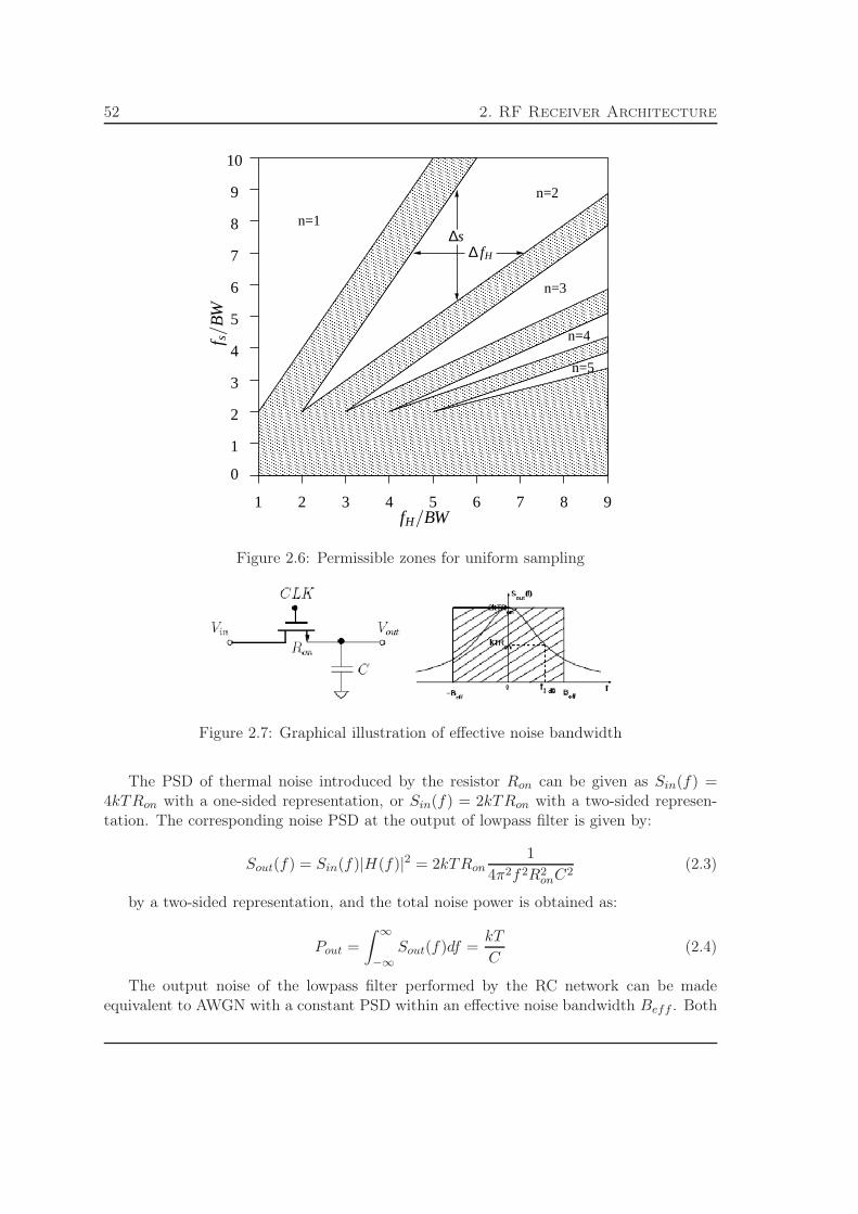
52 2. RF Receiver Architecture
1 2 3 4 5 6 7 8 9
9
8
7
6
5
4
3
2
1
10
0
n=1
n=3
n=4
n=5
n=2
fH/BW
∆ fH
∆sf s/B
W
Figure 2.6: Permissible zones for uniform sampling
Figure 2.7: Graphical illustration of effective noise bandwidth
The PSD of thermal noise introduced by the resistor Ron can be given as Sin(f) =4kTRon with a one-sided representation, or Sin(f) = 2kTRon with a two-sided represen-tation. The corresponding noise PSD at the output of lowpass filter is given by:
Sout(f) = Sin(f)|H(f)|2 = 2kTRon1
4π2f2R2onC2
(2.3)
by a two-sided representation, and the total noise power is obtained as:
Pout =
∫
∞
−∞
Sout(f)df =kT
C(2.4)
The output noise of the lowpass filter performed by the RC network can be madeequivalent to AWGN with a constant PSD within an effective noise bandwidth Beff . Both

53
noise sources share the same noise power kT/C (Fig. 2.7), thus:
Pout =kT
C= 2kTRon · Beff
and
Beff =1
4RonC=
π
2f3dB
The effective noise bandwidth of the sampling device Beff depends on the ON resistanceof the switch and the sampling capacitance, and it is normally larger than the maximumfrequency of the input signal. When using bandpass sampling, the wideband kT/C noisewill be folded due to the effect of subsampling [49] as illustrated in Fig. 2.8.
Figure 2.8: Noise aliasing due to subsampling
In this way, the resulting SNR is lower than the equivalent lowpass sampling system inthe presence of the same noise source. The SNR degradation in dB is given as [44]:
SNRdeg ≈ 10log10Beff
B· B
Fs/2= 10log10
2Beff
Fs(2.5)
In addition to kT/C noise, strong interfering channels placed on alias frequencies arealso folded on top of the useful signal as a result of bandpass sampling, as shown in Fig.2.9. This corrupts the useful signal irreversibly forcing the need of efficient anti-aliasingmechanism.
2.6.3 Bandpass Receiver Configuration
A block diagram of the bandpass-sampling radio receiver architecture is presented in Fig.2.10.
In this receiver architecture, harmonic sampling is used in the RF stage to bring downthe signal frequency from RF to a low IF. The choice of the low-IF is tricky because it hasto be high enough to avoid the aliasing on one hand and it has to be low enough so thatthe ADC and the subsequent DSP can support it. An important thing to notice about thisstructure is that its analog block configuration is much simpler than the classical archi-tectures presented previously. This structure is also known as digital direction conversionreceiver. Its RF front-end consists of two stages of gain adjustable LNA to achieve a lownoise figure and certain gain control range and an RF band-pass SAW filter to suppress

54 2. RF Receiver Architecture
I2I1 I3SA1 A2
I1
I2
I3
S
Fs Fs Fs
(k−1) ·Fs k ·Fs Fc
f
f0 FIF−Fs/2 Fs/2
(k +1) ·Fs
Figure 2.9: Interferers’ aliasing due to subsampling
SinewaveGenerator
Digital
Multiplier
Multiplier
BB LPF
BB LPF
I
Q
BPFRF BPF
PRESELECTOR
LNA2LNA1 RF BPF
sampling
generator
ADC
clock
SamplingHarmonic
Low IFdigital signal
cosωt
sinωt
Input (f0)
Figure 2.10: Bandpass RF sampling receiver architecture
out-of-band interferers and decrease the aliased noise. The filtered and amplified RF signalis then subsampled at the ADC, and the analog RF signal is converted to low-IF digitalsignal.The low-IF digital signal after being equally split in two branches is mixed with apair of quadrature digital LO signals generating base-band digital I and Q signals. Digi-tal low-pass filters are then applied to the base-band I and Q signals to perform channelfiltering. Since the channel filtering is only carried out in the digital domain, the signalattacking the ADC contains strong in-band interferers, and hence, it must have enoughdynamic range to deal with both strong interference and weak useful signal.
The technique of band-pass sampling is not only used for RF signals but also forIF signals. The subsampling of IF signal takes place in a superheterodyne receiver asillustrated in Fig. 2.11.
The remarkable difference between the subsampling superheterodyne receiver and the

55
LNA RF BPF
IRF
sampling
generator
ADC
clock
SamplingHarmonic
SinewaveGenerator
Digital
Multiplier
Multiplier
BB LPF
BB LPF
I
Q
RF BPF
PRESELECTOR
RFA RF DOWNCONVERTER
UHF LO
IFA IF BPF
Low IFdigital signal
cosωt
sinωt
Input (f0)
fLO = | f0− IF|
Figure 2.11: Bandpass IF sampling receiver architecture
classical superheterodyne receiver is that the ADC in the former is moved forward to theIF block output i-e the output of the IF SAW filter. The sampling rate of the ADC is closeto a subharmonic of the IF:
fs =fIF − fLIF
n(2.6)
where n = ⌊fIF
fs⌋. The ADC output, which is a digital signal at IF, is converted to
base-band I and Q signals by the digital quadrature down-converter. The base-band I andQ signals then pass through low-pass filters which act as channel filters to diminish theinterferers near the desired signal.
The key challenge in the band-pass sampling architecture is the design of ADC. Withthe current CMOS technologies in view, the ADC for a band-pass sampling IF signal ismore realistic than for a band-pass sampling RF signal. The bandwidth requirement forADC is much less when subsampling an IF signal as compared to when subsampling anRF signal. The dynamic range requirement for the ADC used in band-pass sampling ofan IF signal is also relaxed (usually 5 to 6 bits) than that applied in band-pass samplingof an RF signal. The reason is that the IF SAW filter in the former case suppresses theinterference level before the signal attacks the ADC and hence reduces the dynamic rangerequirement of the ADC.
2.6.4 Fs/2 IF Bandpass-Sampling Receiver
One interesting category of band-pass sampling receivers is Fs/2 IF bandpass samplingreceiver. This receiver architecture is exposed in Fig. 2.12. It was proposed by STMi-croelectronics and implemented as a discrete-time RF sampling receiver in CMOS 90nmtechnology for the GSM standard [4, 50]. The main difference with the earlier realiza-tions resides in the fact that the intermediate frequency used during downconversion stepsis half the sampling rate (Fs/2). This imposes the following constraint while doing thesubsampling to bring down the signal from carrier frequency Fc to intermediate frequencyFs/2:

56 2. RF Receiver Architecture
Fs =Fc
N + 1/2(2.7)
The RF signal after being passed through low-noise amplifier and bandpass filters issubsampled at first stage from RF to IF. At this stage it is impossible to downconvertthe signal directly to low-IF because the sampling frequency is dictated by the anti-aliasrequirement [4]. To meet GSM requirements, a sampling frequency of 200MHz (Fc/4.5) wasproposed in [4]. If an ADC is used at this sampling frequency, it needs unreasonable powerconsumption. Therefore another stage of subsampling-based downconversion is needed,which brings down the signal at 40MHz which is digitized directly by the high-pass ∆Σmodulators (ADCs).
RF BPF LNA
ADC
generator generatorclockclock
subsampling
ADC
BPF
BPF
BB LPF
I
IFanalog signal
Basebanddigital signal
Low IFdigital signal
BP−AAF
Multiplier
BB LPF
QMultiplier
SinewaveGenerator
Digital
Sampler
Sampler
BP−AAF
BP−AAFHarmonicSampling
subsamplingRF IF
Harmonic
Harmonic
PRESELECTOR
Input (f0)
sinωt
cosωt
π/2 π/2
Figure 2.12: Fs/2 IF sampling receiver architecture
The fact that the signal is forcibly placed at Fs/2 after downconversion makes thisreceiver design to take the advantages of both zero-IF and low-IF structures. Like zero-IFstructures, there is no image signal problem since the image is the conjugate of the usefulsignal itself. Hence, the expensive image reject filters are avoided. Similarly, like low-IFstructures, this solution ensures - with no complexity increase with respect to low-passfilters - that flicker noise and second-order nonlinearity products (IP2) do not degradethe signal. Flicker noise is indeed what limits the CMOS implementations of zero-IFarchitecture for narrow-band standards. To enhance the anti-aliasing capability of thiscircuit, a completely passive anti-aliasing circuit is proposed in [9]. With the similarreceiver architecture as [4, 50], and using this better anti-aliasing technique [9], an RFreceiver chain is defined in [3] which addresses two wireless protocols i-e GSM and WiFi.This receiver scheme is illustrated in Fig. 2.13 and its functionality is explained in detailin the follwing sections.
It comprises of an RF filter, a transconductance LNA, two discrete-time analog signalprocessing stages (DTASPs) and ADCs. The RF input signal is first filtered, amplifiedand converted to a current. It is then fed to the first DTASP block, where it gets IIR/FIRfiltered and quadrature downconverted to the first intermediate frequency. A second down-conversion stage further decimates the sampling rate and filters the IF signal before it isfinally digitized.

57
Figure 2.13: Dual-Mode Fs/2 discrete-time sampling receiver [3]
2.6.4.1 RF Stage
RF filters limit the reconfigurability of multistandard receivers and current research workstowards the suppression of these filters. In this design however, the RF filter was conserved,as it relaxes the requirements on both the LNA and anti-alias filter. Only one transcon-ductance LNA is used and its current is permanently switched between the in-phase andquadrature paths. This minimizes the I/Q gain mismatches and improves the image re-jection of the receiver. The drawback is that the integration period is halved, which inturn halves the LNA gain. Great attention must be paid to the generation of the clocksignals because a slight overlapping between I/Q successive sampling phases can shortenthe quadrature paths and corrupt the useful signal.
2.6.4.2 First DTASP Stage
The LNTA output current is integrated during a Tc/4 time interval, alternately betweenthe I and Q paths. This results in a sampled data stream with a sampling rate of 2Fc
per quadrature path. The IIR filter is employed to prevent the LNTA’s output fromsaturating and is made up of a single pole. However, in contrast to the previous GSMreceiver [4], in this receiver architecture, it precedes the AAF/decimation stage, resultingin the capacitors’ switching at a rate of 2Fc rather than Fs. The operation of the 1stDTASP block is illustrated in Fig. 2.14 for comprehension.
It is a series combination of current integrator, voltage sampler and discrete-time IIRfilter. The transition from continuous-time to discrete-time occurs at the output of thesimplistic sampler. The first decimation stage is preceded by a 2nd order anti-alias filter,which theoretically squares the rejection achieved in the previous design. The desiredsignal is downconverted through the decimation process to a first intermediate frequencyand fed to a second DTASP block. The RF signal is sampled at a rate of 2Fc which resultsin a first spectrum folding, depicted in Fig. 2.15.
It is important to note that this first sampling doesn’t have any dedicated anti-aliasfilter and benefits only from the attenuations brought by the RF SAW and continuous-timesinc filters. The desired signal at frequency Fc is not shifted during the sampling process,
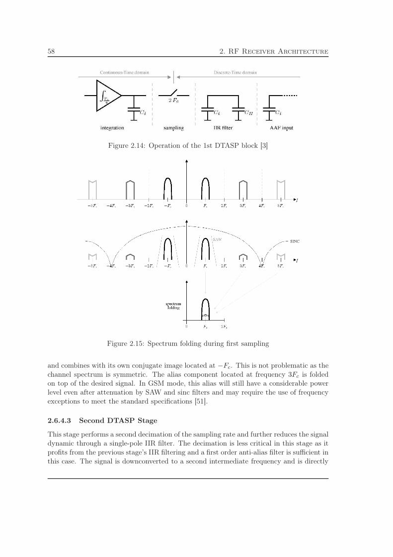
58 2. RF Receiver Architecture
Figure 2.14: Operation of the 1st DTASP block [3]
Figure 2.15: Spectrum folding during first sampling
and combines with its own conjugate image located at −Fc. This is not problematic as thechannel spectrum is symmetric. The alias component located at frequency 3Fc is foldedon top of the desired signal. In GSM mode, this alias will still have a considerable powerlevel even after attenuation by SAW and sinc filters and may require the use of frequencyexceptions to meet the standard specifications [51].
2.6.4.3 Second DTASP Stage
This stage performs a second decimation of the sampling rate and further reduces the signaldynamic through a single-pole IIR filter. The decimation is less critical in this stage as itprofits from the previous stage’s IIR filtering and a first order anti-alias filter is sufficient inthis case. The signal is downconverted to a second intermediate frequency and is directly

59
fed to the ADC.
2.6.4.4 Frequency Plans
The frequency plans of this receiver architecture, adopted for each of the GSM/WIFImodes, are detailed in this section. Values for decimation ratios, sampling and intermediatefrequencies are derived as well.
GSM Mode The frequency plan of the GSM mode is depicted in Fig. 2.16. The desiredsignal is always centered at half the sampling frequency (Fs/2) to avoid degradations causedby flicker noise and IP2 products and is assured by setting the decimation ratios to oddvalues.
Figure 2.16: GSM mode frequency plan [3]
The first decimation ratio is dictated by the anti-alias requirement, since alias rejectionis directly proportional to signal bandwidth over sampling frequency ratio. For a secondorder anti-alias filter, this rejection is given by:
20log(2Fs
BW)2 ≥ Palias − SdBm + SNRmin (2.8)
which imposes a minimum sampling frequency of:
Fs,min =200KHz
2· 10−111/40 ≃ 60MHz (2.9)
Note that this expression does not account for the attenuation brought by the SAWfilter, and even in this case, has resulted in a considerably low sampling frequency. This ishowever a theoretical value. In practice, capacitor mismatches at circuit level degrade thenotches of the anti-alias filter and force the use of much higher sampling frequencies.
Another drawback of setting a low value for the sampling frequency is that, it results ina high decimation ratio, which in turn increases the complexity of the filter circuit design(longer rotating capacitor banks). The first decimation ratio was therefore set to M1 = 5,leading to a sampling frequency of 360 MHz and to a first intermediate frequency of 180MHz.
The second DTASP stage had to adapt the sampling rate to the 40 MS/s ∆Σ ADCconstraint. The second decimation ratio was thus set to M2 = 360/40 = 9 and the signalwas downconverted to a second intermediate frequency of 20 MHz.

60 2. RF Receiver Architecture
WiFi Mode In WiFi mode, owing to the large channel bandwidth, the flicker noisebecomes less significant. Fs/2 architecture is not considered necessary anymore and thedesired signal is downconverted and processed directly at DC (Zero IF). The RF signal isfirst sampled at twice the channel frequency (2Fc), as in the GSM mode. IIR and anti-aliasfilters are still centered around the RF channel. The signal is then downconverted to DCby setting the decimation ratio to an even value.
In this configuration, the RF stage remains unchanged and the anti-alias filter is theonly block that has to be reconfigured. The frequency plan for WiFi mode is given inFig. 2.17. Only the first DTASP stage was actually implemented on circuit. The seconddownconversion stage and the ADC are added to give a complete illustration of the receiver.
Figure 2.17: WIFI mode frequency plan [3]
Like in GSM mode, the first decimation ratio is dictated by the alias rejection require-ments. Using the same second order anti-alias filter, the minimum sampling frequency isnow equal to :
Fs,min =20MHz
2· 10(−20+65+21.1)/40 ≃ 450MHz (2.10)
The sampling frequency was set to a much higher value than the minimum required, toaccount for notch degradations at circuit level. The decimation ratio was set to M1 = 4 inorder to facilitate the reconfigurability of the anti-alias filter. Once downconverted to DC,the signal is buffered and outputted for measurement. The second DTASP stage (whichwas not implemented) includes a first order anti-alias filter, a decimation by M2 = 2 anda single pole IIR filter. The sampling rate is lowered to 600 MHz and the signal is fed tothe ADC for digitization.
2.6.4.5 Proposed Frequency Plans
After studying the recent state-of-the-art RF receiver front-ends, and keeping in viewthe available ADC performances which are detailed in the next chapters, the frequencyplan illustrated in Fig. 2.18 is proposed. Note that in contrast to the receiver front-endpresented earlier [3], Fs/2 architecture is adopted for both the protocols to stay clear fromFlicker noise and dc-offsets throughout the signal processing.
The ADC for GSM mode runs at the speed of 28.57MHz, while the ADC for WiFimode is configured to operate at 228.57MHz.

61
(a)
(b)
IIR 1FIR 1
FIR 2 IIR 2 ADC2.4GHz
7 3
IIR 1FIR 1
7 FIR 2 9 IIR 2 ADC900MHz
Fc
2nd DTASP1st DTASP
1st DTASP 2nd DTASP
(SINC2)
(SINC2)
Fs = 228.57MHzsignal @Fs/2
Fs = 28.57MHzsignal @Fs/2
Fc
Fs = 1.8GHzsignal @Fc signal @Fs/2
Fs = 257.14MHz
Fs = 685.71MHzsignal @Fs/2signal @Fc
Fs = 4.8GHz
Figure 2.18: (a) GSM mode frequency plan, (b) WIFI mode frequency plan
2.7 Conclusion
The RF front-ends of various competing radio receiver architectures are discussed in thischapter. Superheterodyne receiver topology is the most commercially popular RF receiverbecause of its performance. To cater for the increased constraints on receiver front-endsthese days, including integrability and reconfigurability, newer and innovative receivertopologies are being introduced. Digital IF receiver is exposed, which is a type of Su-perheterodyne architecture where the signal is digitized in the IF stage. Direct Conversionreceiver is explained which has the advantages of simplicity and reduced component count.It gets rid of the components which are difficult to the integrated. But it has the problemsof imbalance between I and Q signal paths, dc-offset and flicker noise directly corruptingthe signal. Low-IF receiver gets rid of the problems associated with direct-conversion re-ceiver but it introduces its own problem i-e image signal corrupting the useful signal afterdown-conversion. Image-reject filters need to be introduced which are expensive. To makethe receivers integrable, reconfigurable and flexible (realization of software radio concept),the technique of bandpass sampling is used which helps in reducing the analog componentcount by digitizing the signal at earlier stages in the front-end receiver. One application ofthis reception technique is the recently introduced receiver architecture : Fs/2 IF receiver.It solves the problems of both direct-conversion and low-IF receivers, while enjoying theadvantages of both of them. In this architecture, the sampling frequency is selected suchthat after downconversion, the useful signal falls at half of the sampling frequency. Asa result, the image is the conjugate of the signal, hence avoiding the image-reject filters.Moreover, since the signal is centered at IF = Fs/2, the dc-offsets of various componentsand device flicker noise do not corrupt the signal. To directly digitize this signal, a specialkind of ADC, called high-pass ∆Σ modulator, is required.
In the research work conducted at our laboratory, all the blocks in the receiver chainfor multi-mode operation have already been designed [3], with a special focus on efficientanti-alias filter design [9]. The objective of the rest of this research work is to propose and

62 2. RF Receiver Architecture
design an efficient ADC i-e high-pass ∆Σ modulator that can support multiple wirelessstandards and be integrated in the receiver chain already designed.

63
Chapter 3
∆Σ Modulator and System LevelModeling
3.1 Introduction
ADCs with high resolution are widely used in the areas of instrumentation, measurement,telecommunications, digital signal processing, consumer electronics, etc. With the ad-vancements in the Very Large Scale Integration (VLSI) technologies, the focus is shiftedon oversampling and ∆Σ converters for applications requiring high precision analog-to-digital conversion with narrow bandwidth [52, 12, 10, 53]. They are preferred because oftheir inherent relaxed sensitivity to analog circuit errors and reduced analog processingas compared to other analog-to-digital conversion techniques. These advantages come atthe expense of relatively large amount of digital processing and the working of the majorpart of circuit at a clock rate which is much higher than the analog-to-digital conversionrate. Because of using higher clock rates and feedback loop, these converters tend to berobust in the face of analog circuit imperfections [52] and do not require trimmed compo-nents which are considered necessary in conventional high precision Nyquist rate ADCs.Because of these reasons high precision ∆Σ ADCs can be implemented using high densityVLSI processes. These processes are optimized for digital circuitry where analog accuracyis sacrificed for circuit density and speed. Thus, the integration capability of ∆Σ ADCs inthese processes makes it possible to design integrated, smaller, robust and less expensivesystems.
∆Σ ADC is a system which consists of a ∆Σ modulator followed by a digital decima-tion filter. The ∆Σ modulator over-samples the input signal i-e performs sampling at arate much higher than the nyquist rate. The ratio of this rate to the Nyquist rate is calledover-sampling ratio (OSR). After over-sampling, it typically performs very coarse analog-to-digital conversion at the resulting narrow-band signal. By using coarse digital-to-analogconversion and feedback, the quantization error introduced by the coarse quantizer is spec-trally shaped i-e the major portion of the noise power is shifted outside the signal band.This process is called quantization noise shaping. The digital decimation filter removes theout-of-band portion of the quantization error and brings back the output rate to Nyquist

64 3. ∆Σ Modulator and System Level Modeling
rate.This entire process of oversampling coupled by quantization noise shaping and deci-
mation filtering results in high precision ADC despite the fact that coarse ADC and DACare used. In particular, 1-bit ADC and 1-bit DAC are often employed which have theadded advantage that static errors in their outputs only affect the gain and offset of thesystem without introducing any distortion. Another advantage of oversampling is the re-laxed requirements on analog anti-aliasing filter because much of the required anti-aliasingfunctionality is provided by the digital decimation filter.
In this chapter, the principle of ∆Σ modulation is explained, single-loop second-orderarchitectures are exposed and various higher order topologies are discussed. Multibit quan-tizer techniques along with their inherent problems and their solutions are presented. Con-tinuous time (CT) ∆Σ modulators are introduced, followed by recently published hybrid(CT and DT) structures. In the end, system level modeling of various components, includ-ing quantizer, op-amp and comparator is presented along with simulation results.
3.2 Working Principle
The basic working of ∆Σ ADC is that it exchanges output resolution with conversion speed.In such ADC, the analog signal is converted into a low resolution code at a frequencymuch higher than the Nyquist rates, and then the excess quantization noise is removedby the following digital filters [10]. Thus, if OSR is high, the oversampling ∆Σ ADCsare very suitable for CMOS VLSI digital technology, because they do not require highperformance analog building blocks. Fig. 3.1 shows the basic block diagram of a Delta-Sigma modulator and its corresponding linear model. The Delta-Sigma modulator consistsof a feedforward path formed by a loop filter and a B-bit quantizer, and a negative feedbackpath around them, using a B-bit DAC [11]. In the linear model as illustrated in Fig. 3.1, theDAC is assumed to be ideal and the injected quantization error is assumed as an additivewhite noise approximation. Although this approximation is not valid for low-resolutionquantizers, it is nonetheless used for simplicity of calculations.
−−
(b)(a)
H(z)H(z)
DAC
B
DAC
Qin
E
YXYXQin
Figure 3.1: Basic ∆Σ Modulator (a) Block diagram, (b) Corresponding linear model
In this way, the modulator can be considered as a two-input, one-output linear system.The signal transfer function, STF (z) of this system is:
STF (z) =Y (z)
X(z)=
H(z)
1 + H(z)(3.1)

65
and the noise transfer function, NTF (z) is:
NTF (z) =Y (z)
E(z)=
1
1 + H(z)(3.2)
By using superposition principle, the output signal is obtained as the combination ofthe input signal and the noise signal, with each being filtered by the corresponding transferfunction:
Y (z) = STF (z)X(z) + NTF (z)E(z) (3.3)
By properly selecting the loop filter, the signal transfer function and the noise transferfunction of a theoretical 1st order ∆Σ modulator yield in the z-domain:
STF (z) = z−1 (3.4)
NTF (z) = (1 − z−1) (3.5)
Solving Eqns. 3.1 and 3.4 gives:
H(z) =z−1
1 − z−1(3.6)
Note that loop-filter is simply an integrator which can be easily implemented withswitched-capacitor techniques. For a generalized Lth order ∆Σ modulator, the transferfunctions become:
STF (z) = z−L (3.7)
NTF (z) = (1 − z−1)L (3.8)
To achieve a transfer function of Lth order, L basic building blocks i-e L integratorsare required. Fig. 3.2 plots the frequency responses of NTF s with different values of L.When the modulator order is higher than one, the frequency response of NTF presents thecharacteristic of high-pass filters. The higher the order L is, the more quantization errorenergy is suppressed at low frequencies.
In this way, the output signal for the ideal linear model can be written as:
Y (z) = X(z)z−L + E(z)(1 − z−1)L (3.9)
The input signal X(z) experiences just L delays as it passes through the modulator,while the quantization noise E(z) experiences an Lth order high-pass filtering as it makesits way through Lth order ∆Σ modulator. If the quantization step is small compared to thequantizer input amplitude, the quantization error can be assumed to be a random process.Taking ∆ as the quantization step, the quantization error is bound between [−∆/2 ↔ ∆/2]with a uniform probability density of 1/∆ [54]. The variance of the quantization error iscalculated as:

66 3. ∆Σ Modulator and System Level Modeling
0 0.05 0.1 0.15 0.2 0.25 0.3 0.35 0.4 0.45 0.50
2
4
6
8
10
12
14
16
Normalized Frequency
|NT
F|
L=1
L=2
L=3
L=4
Figure 3.2: Frequency responses of NTFs for different modulator orders L
e2 = σ2(e) =1
∆
∫ ∆/2
−∆/2e2de =
∆2
12(3.10)
Hence, the in-band power of the filtered quantization error is found to be:
PQ =
∫ fb/2
−fb/2
∆2
12|NTF (f)|2df ≈
∆2
12
π2L
(2L + 1)OSR2L+1(3.11)
Ideally, the full-scale range of the modulator input is approximately given by that of thequantizer. In a B-bit quantization case, this range equals ±(2B − 1)∆/2, so the full-scaleinput amplitude is (2B − 1)∆/2 and its power at the ADC output can be approximatedto:
Psignal∼= (AFS)2
2=
(
(2B − 1)∆2
)2
2≈ 22B−3∆2 (3.12)
Using Eqns. 3.11 and 3.12, the dynamic range (DR) of an ideal oversampling noise-shaping converter yields:
DR(dB) ≈ 10log10
[
3
2
(2L + 1)
π2LOSR2L+1(2B − 1)2
]
(3.13)
The theoretical DR is a function of the modulator order L, oversampling ratio OSR,and the numbers of bits in the quantizer B. Equation 3.13 reveals that an additional bit in
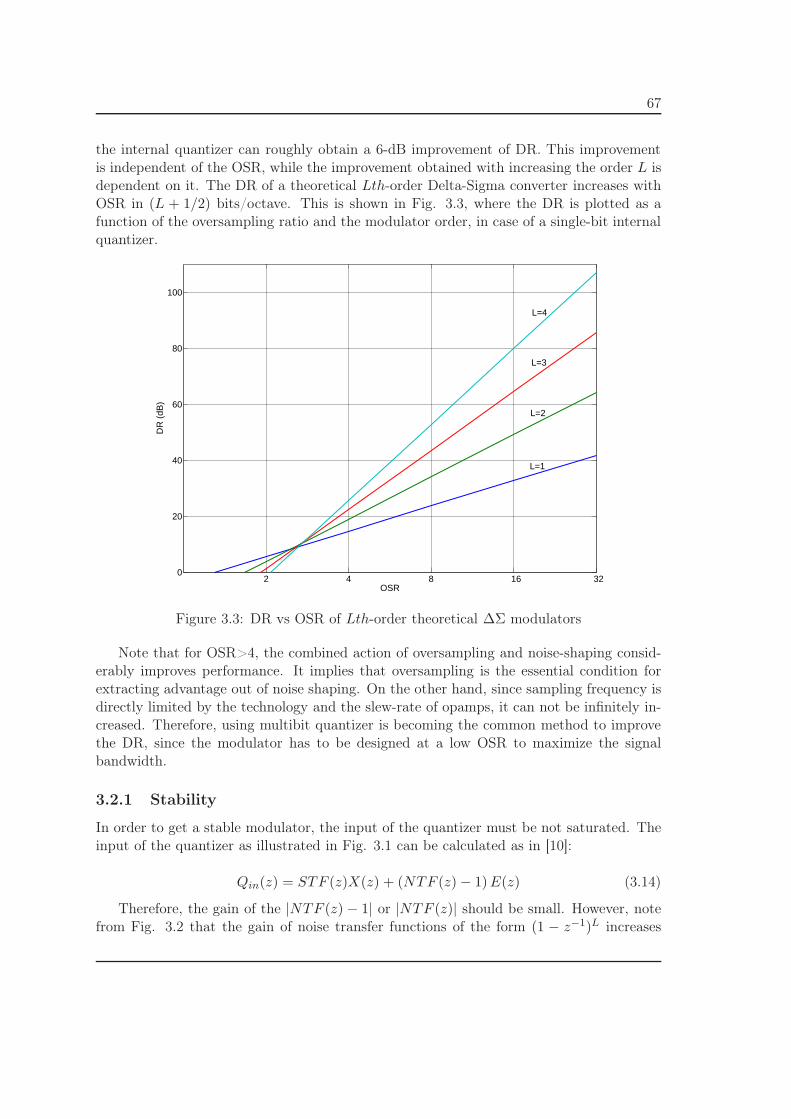
67
the internal quantizer can roughly obtain a 6-dB improvement of DR. This improvementis independent of the OSR, while the improvement obtained with increasing the order L isdependent on it. The DR of a theoretical Lth-order Delta-Sigma converter increases withOSR in (L + 1/2) bits/octave. This is shown in Fig. 3.3, where the DR is plotted as afunction of the oversampling ratio and the modulator order, in case of a single-bit internalquantizer.
2 4 8 16 320
20
40
60
80
100
OSR
DR
(dB
)
L=1
L=4
L=2
L=3
Figure 3.3: DR vs OSR of Lth-order theoretical ∆Σ modulators
Note that for OSR>4, the combined action of oversampling and noise-shaping consid-erably improves performance. It implies that oversampling is the essential condition forextracting advantage out of noise shaping. On the other hand, since sampling frequency isdirectly limited by the technology and the slew-rate of opamps, it can not be infinitely in-creased. Therefore, using multibit quantizer is becoming the common method to improvethe DR, since the modulator has to be designed at a low OSR to maximize the signalbandwidth.
3.2.1 Stability
In order to get a stable modulator, the input of the quantizer must be not saturated. Theinput of the quantizer as illustrated in Fig. 3.1 can be calculated as in [10]:
Qin(z) = STF (z)X(z) + (NTF (z) − 1) E(z) (3.14)
Therefore, the gain of the |NTF (z) − 1| or |NTF (z)| should be small. However, notefrom Fig. 3.2 that the gain of noise transfer functions of the form (1 − z−1)L increases
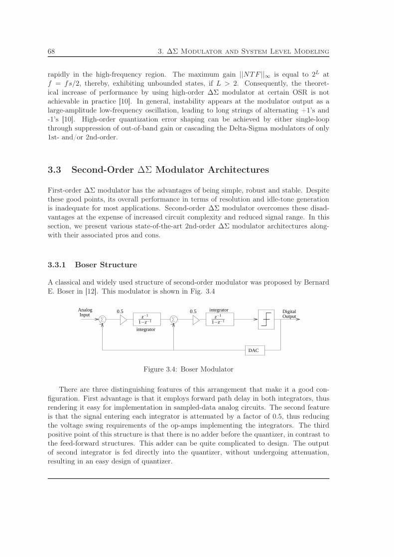
68 3. ∆Σ Modulator and System Level Modeling
rapidly in the high-frequency region. The maximum gain ||NTF ||∞ is equal to 2L atf = fs/2, thereby, exhibiting unbounded states, if L > 2. Consequently, the theoret-ical increase of performance by using high-order ∆Σ modulator at certain OSR is notachievable in practice [10]. In general, instability appears at the modulator output as alarge-amplitude low-frequency oscillation, leading to long strings of alternating +1’s and-1’s [10]. High-order quantization error shaping can be achieved by either single-loopthrough suppression of out-of-band gain or cascading the Delta-Sigma modulators of only1st- and/or 2nd-order.
3.3 Second-Order ∆Σ Modulator Architectures
First-order ∆Σ modulator has the advantages of being simple, robust and stable. Despitethese good points, its overall performance in terms of resolution and idle-tone generationis inadequate for most applications. Second-order ∆Σ modulator overcomes these disad-vantages at the expense of increased circuit complexity and reduced signal range. In thissection, we present various state-of-the-art 2nd-order ∆Σ modulator architectures along-with their associated pros and cons.
3.3.1 Boser Structure
A classical and widely used structure of second-order modulator was proposed by BernardE. Boser in [12]. This modulator is shown in Fig. 3.4
OutputAnalogInput
Digital
DAC
− −integrator
integrator0.5 0.5z−1
1−z−1z−1
1−z−1
Figure 3.4: Boser Modulator
There are three distinguishing features of this arrangement that make it a good con-figuration. First advantage is that it employs forward path delay in both integrators, thusrendering it easy for implementation in sampled-data analog circuits. The second featureis that the signal entering each integrator is attenuated by a factor of 0.5, thus reducingthe voltage swing requirements of the op-amps implementing the integrators. The thirdpositive point of this structure is that there is no adder before the quantizer, in contrast tothe feed-forward structures. This adder can be quite complicated to design. The outputof second integrator is fed directly into the quantizer, without undergoing attenuation,resulting in an easy design of quantizer.
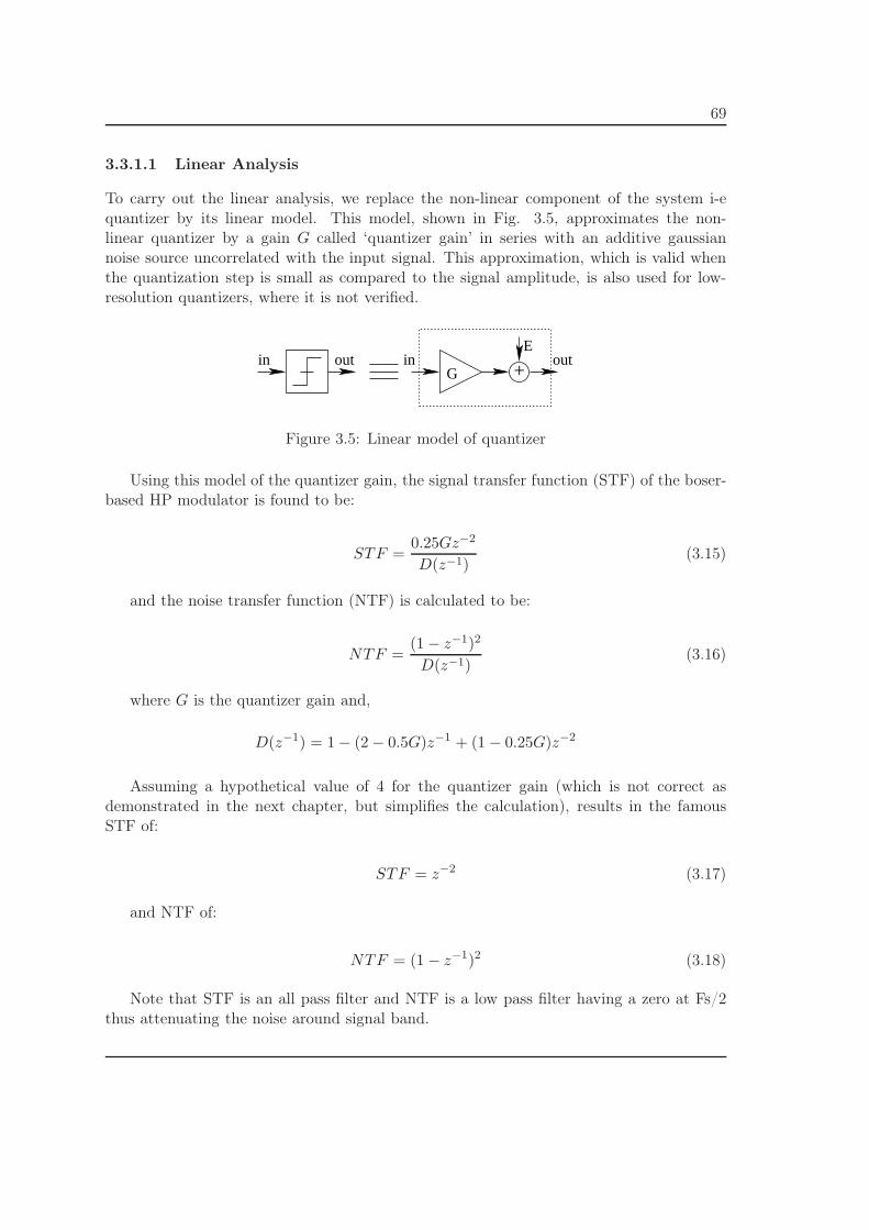
69
3.3.1.1 Linear Analysis
To carry out the linear analysis, we replace the non-linear component of the system i-equantizer by its linear model. This model, shown in Fig. 3.5, approximates the non-linear quantizer by a gain G called ‘quantizer gain’ in series with an additive gaussiannoise source uncorrelated with the input signal. This approximation, which is valid whenthe quantization step is small as compared to the signal amplitude, is also used for low-resolution quantizers, where it is not verified.
G
E
+in outoutin
Figure 3.5: Linear model of quantizer
Using this model of the quantizer gain, the signal transfer function (STF) of the boser-based HP modulator is found to be:
STF =0.25Gz−2
D(z−1)(3.15)
and the noise transfer function (NTF) is calculated to be:
NTF =(1 − z−1)2
D(z−1)(3.16)
where G is the quantizer gain and,
D(z−1) = 1 − (2 − 0.5G)z−1 + (1 − 0.25G)z−2
Assuming a hypothetical value of 4 for the quantizer gain (which is not correct asdemonstrated in the next chapter, but simplifies the calculation), results in the famousSTF of:
STF = z−2 (3.17)
and NTF of:
NTF = (1 − z−1)2 (3.18)
Note that STF is an all pass filter and NTF is a low pass filter having a zero at Fs/2thus attenuating the noise around signal band.

70 3. ∆Σ Modulator and System Level Modeling
3.3.1.2 Disadvantage of Boser Structure
Boser-based structure is basically a feedback-only structure. The input signal has to tra-verse through all the integrators to reach the quantizer. The principal disadvantage of thisstructure thus stems from the fact that the signal entering the integrators consists of notonly the quantization noise, but also the input signal. Any op-amp non-linearity in theintegrators directly generates the input signal harmonics in the signal band, thus degradingthe signal-to-noise-and-distortion-ratio (SNDR).
3.3.2 Silva Structure
José Silva working at Oregon State University revolutionized the ∆Σ architectures byproposing a new architecture in [13] which took care of the shortcoming of Boser architec-ture. His proposed architecture is shown in Fig. 3.6
OutputAnalogInput
Digitalintegrator
DAC
integrator−
2
z−1
1−z−1z−1
1−z−1
Figure 3.6: Silva Modulator
This architecture is basically feedforward in nature; input signal is fed directly to thequantizer and thus does not have to traverse the integrators. As a result, the non-linearitiesof the op-amps constituting the integrators do not distort the input signal. This is why,this architecture is also called low-distortion architecture. The refined version of thisarchitecture with optimized coefficients is presented in [55] and shown in Fig. 3.7.
OutputDigital
integrator
integrator
−
DAC
AnalogInput
0.50.5
4/9
z−1
1−z−1z−1
1−z−1
4/9
1/9
Figure 3.7: Optimized version of Silva Structure (Rusu Structure)
It has to be noted that the sum of the coefficients before the comparator is one; withthis set of coefficients, the adder can be implemented passively. Passive adder reduces thepower consumption of the circuit by avoiding the use of an op-amp (active adder). Usingan active adder is basically equivalent to utilizing the resources of a third-order modulatorwhile getting the performance of only a second-order modulator.

71
3.3.2.1 Linear Analysis
Replacing the quantizer by its linear model as shown in Fig. 3.5 and discussed in Section.3.3.1.1 and performing the analysis of refined Silva-based structure results in the STF of:
STF =G/9
D(z−1)(3.19)
and similarly the NTF is found to be:
NTF =(1 − z−1)2
D(z−1)(3.20)
where G is the quantizer gain and,
D(z−1) = 1 − (2 − 2G
9)z−1 + (1 − G
9)z−2
Assuming a value of 9 for G (for the ease of calculation) results in:
STF = 1, NTF = (1 − z−1)2 (3.21)
Since STF is one, the input signal is cancelled out at the input of first integrator andhence the linearity requirements of the op-amp are very relaxed resulting in its easy design.
3.3.2.2 Disadvantages of Silva Structure
The Silva structure uses one adder before the quantizer. It can be implemented as eitherpassive or active adder. In the case of using a passive adder, we reduce the signal swingat the 2nd integrator output because of additional parasitic capacitances of the summingnode [14]. Passive adder also increases the design requirements of comparator because itsinput signal is attenuated and thus it needs higher sensitivity. The other possibility is usingan active adder. Active adder on the other hand involves an opamp, which increases thepower consumption of the modulator. The second problem associated with this structureis that the first opamp has to charge both the sampling capacitor of the second opamp,and the feedforward capacitor which is used for implementing the adder. Thus it increasesthe capacitive loading on the amplifier hence augmenting its power consumption.
3.3.3 Oberst Structure
A new modulator architecture has been proposed recently in literature [14], which ishalfway between feedback and feedforward architectures. Its operation is illustrated inFig. 3.8. This modulator uses the advantages of both Boser and Silva structures i-e thereis no adder before the quantizer and the input signal attacks directly the second integrator,thus the first integrator, which is the most critical one does not process the input signalresulting in relaxed requirements of the opamp. The distortions generated in the secondintegrator are first-order noise-shaped and hence are less critical.

72 3. ∆Σ Modulator and System Level Modeling
OutputDigital
DAC
AnalogInput
− −integrator
integrator0.5 0.5
0.25
0.25z−1
z−1
1−z−11
1−z−1
Figure 3.8: Oberst Structure
3.3.3.1 Linear Analysis
Replacing the quantizer by its linear model as shown in Fig. 3.5 and discussed in Section.3.3.1.1 and performing the analysis of Oberst structure results in the STF of:
STF =G/4
D(z−1)(3.22)
and similarly the NTF is found to be:
NTF =(1 − z−1)2
D(z−1)(3.23)
where G is the quantizer gain and,
D(z−1) = 1 − (2 − G
2)z−1 + (1 − G
4)z−2
Assuming a value of 4 for G results in:
STF = 1, NTF = (1 − z−1)2 (3.24)
Unity STF results in the cancellation of useful signal at the input to the first integrator,and hence the non-linearities of its op-amp do not generate distortions. On the other hand,the signal entering the second integrator contains a portion of input signal, hence its non-idealities corrupt the useful signal appearing at the output.
3.3.3.2 Disadvantages of Oberst Structure
The Oberst architecture is still constrained by the nonlinearities of the opamp which im-plements the second integrator, even though they are first-order noise shaped. The otherdisadvantage arises from the fact that the second integrator is a delay less filter and thusthe capacitive loading on the opamp comprising the first filter increases during the inte-gration phase, since it has to charge both its own feedback capacitor and the samplingcapacitor of the next filter. The third disadvantage is the use of small coefficients 0.25for second integrator in this architecture. For the implementation of this small coefficient,we have to use an integration capacitor of (1/0.25)Cs = 4Cs, which makes a big capaci-tor value and thus results in higher power consumption for charging this capacitor. The

73
fourth disadvantage is the presence of feedback with a delay. This complicates the designnecessitating an extra capacitor.
3.4 Higher-Order ∆Σ Modulator Architectures
There are two existing techniques to achieve higher-order ∆Σ modulation 1)Single loophigher order 2)MASH (Multi-stAge noise SHaping) or cascaded higher order. Single looparchitectures are affected by the unstability of modulator due to excess gain of NTF in highfrequecies. To counter this problem various techniques have been adopted which attenuatethe NTF gain in high frequecies at the expense of higher NTF gain at low frequencies thusdegraded signal to quantization ratio (SQNR). MASH topologies on the other hand areunconditionally stable since they are formed by cascade of lower order modulators. Theyare prone to noise leakage because of analog and digital components mismatch.
3.4.1 Single-Loop Higher-Order
As discussed earlier in Section. 3.2 and shown in Fig. 3.2, the gain of the noise transferfunction of the form (1−z−1)L increases exponentially in the high-frequency region reachingits maximum value ||NTF ||∞ of 2L at f = Fs/2, where L is the modulator order. For singleloop modulator with one bit internal quantizer to remain stable, Lee’s rule [56] dictatesthat this gain must be smaller than 1.5. There are two techniques to attenuate the NTFgain at high frequencies, the first one converts NTF to Butterworth filter while the otherone changes NTF to inverse Chebyshev filter. Both of these techniques result in loss ofSQNR due to higher gain of NTF in the signal band. Butterworth filter is obtained by aclassic cascade of integrators by choosing the appropriate coefficients. It has an NTF ofthe form:
NTFButterworth =(1 − z−1)L
D(z)(3.25)
Where (1 − z−1)L is the noise-shaping factor, and D(z) is the Lth-order polynomialwhich reduces the NTF gain at high frequencies. Since, all the zeros are placed on dc, theNTF has a good response at dc level, but it degrades at higher frequencies [10].
NTF can be further improved by placing notches in the signal band for further shapingof the quantization noise, while preserving its controlled high-frequency gain, and thereforemaintaining the modulator stability. This type of response is provided by inverse Cheby-shev filter which is realized by placing local feedback loops around integrators to formresonators [57]. NTF achieved with this filter is given by:
NTFinverseChebyshev =(1 − z−1)LG(z)
D(z)(3.26)
where G(z) results in generating optimal complex-conjugate pairs of zeros which createripples at the stop band of the signal. The zeros are optimally spread over the bandresulting in in-band noise power reduction of 13dB relative to the Butterworth filter for

74 3. ∆Σ Modulator and System Level Modeling
4th order modulator [58]. As a result, the maximum achievable SQNR of Lth-order inverseChebyshev filters is higher than that of Butterworth filters. However, in comparison withthe theoretical NTF, the in-band noise attenuation of both alternatives is poor.
3.4.1.1 Cascade of integrators with distributed feedback (CIFB) structure
The generalized Lth-order cascade of integrators with distributed feedback as well as dis-tributed input coupling (CIFB) structure is shown in Fig. 3.9. It consists of L cascadeddelaying-integrators, with the feedback signal as well as the input signal being fed to eachintegrator with different weight factors ai and bi respectively.
Input
Output
− − − − −
b1 b2 b3 b4
a1 a2 a3 a4
c1 c2 c3z−1
1−z−1z−1
1−z−1z−1
1−z−1z−1
1−z−1
aL
bL bL+1cL
z−1
1−z−1
Q
Figure 3.9: Generalized Lth-order CIFB structure
The scaling coefficients ci are used to control the output excursions of integrators. TheNTF of this configuration is of the form:
NTF =(1 − z−1)L
D(z)(3.27)
where,
D(z) = a1c1c2 · ·cLz−L +a2c2c3 · ·cLz−L+1(1−z−1)+ · · ·+aLcLz−1(1−z−1)L−1 +(1−z−1)L
(3.28)Note that this NTF has Butterworth filter characteristics with L zeros at dc. Coeffi-
cients ai alongwith scaling coefficients ci determine the pole locations of NTF and havenon-zero values to stabilise the modulator. The STF is given by:
STF =b1c1c2 · ·cLz−L + b2c2c3 · ·cLz−L+1(1 − z−1) + · · · + bL+1(1 − z−1)L
D(z)(3.29)
where D(z) is given in Eqn. 3.28. This indicates that the bi and ci determine the STFzeros while ai and ci fix the poles. There is some latitude in choosing the zeros of the STF,and hence bi. A good choice is bi = ai for all i ≤ L and bL+1 = 1 [59], which results inunity STF. Thus, the input signal is not processed by any integrator and the loop filteronly processes the quantization noise. This has two advantages: 1) op-amp output swingsare reduced, 2) the unavoidable nonlinearities of the integrators do not introduce harmonicdistortion into the output signal.

75
3.4.1.2 Cascade of resonators with distributed feedback (CRFB) structure
A modification of CIFB structure which implements cascade of resonators instead of inte-grators thus called CRFB structure is shown in Fig. 3.10. Much better SQNR performanceis achieved as NTF zeros are distributed on unit circle producing notches in the signal bandand hence creating an inverse Chebyshev filter response.
− − − − −
AnalogInput
OutputDigital
c1 c2 c31
1−z−1z−1
1−z−1z−1
1−z−1
cLz−1
1−z−1
−g1 −g2b1 b2 b3 b4 bL bL+1
Qa1 a2 a3 a4 aL
11−z−1
Figure 3.10: Cascade of resonators with distributed feedback (CRFB structure)
If the modulator order is even, the normalized zero frequencies are given by [60]:
ωi ≈√
gi (3.30)
In case of odd-modulator order L, a plain integrator is used, preferably in the inputstage to minimize the input-referred noise contribution from subsequent stages.
All the resonators have one delay-free integrator to ensure that the poles stay on unitcircle. In case of switched-capacitor implementations, using a combination of delay-freeand delaying integrators increases the speed requirements of the amplifiers used. Thereforedelaying integrators only are used for resonators. The poles in such situations fall outsidethe unit circle. To stabilise the resonators, they are placed in stable feedback system whichprevents local oscillations.
3.4.1.3 Cascade of integrators with distributed feedforward (CIFF) structure
An alternative procedure to realize the NTF is using feedforward, rather than feedback,signal paths. A topology constructed from cascaded integrators and feedforward branchesis shown in Fig. 3.11
The NTF is given by:
NTF =(1 − z−1)L
D(z)(3.31)
where,
D(z) = aLc1c2··cL−1z−L+aL−1c2c3··cL−2z
−L+1(1−z−1)+···+a1z−1(1−z−1)L−1+(1−z−1)L
(3.32)An interesting case is, bi = 0 for all i ≤ L and b1 = bL+1 = 1. This results in unity STF
structure [60], and hence the low-distortion characterstic as discussed for CIFB structure.

76 3. ∆Σ Modulator and System Level Modeling
−
AnalogInput
OutputDigital
Q
b1 b2 b3 b4 bL bL+1
c3c2c1z−1
1−z−1z−1
1−z−1z−1
1−z−1z−1
1−z−1z−1
1−z−1
a1 a2 a3 a4 aL
Figure 3.11: Cascade of integrators with distributed feedforward (CIFF structure)
3.4.1.4 Cascade of resonators with distributed feedforward (CRFF) structure
High SQNR version of CIFF is CRFF structure with local feedback loops around integra-tors. It implements inverse Chebyshev filter response by optimally placing zeros in signalband. Fig. 3.12 illustrates the CRFF topology, where for simplicity only the first and lastinput weight factors are included, to obtain the low-distortion structure.
−
InputAnalog
OutputDigital
Q
c3c2c1z−1
1−z−1z−1
1−z−1z−1
1−z−1z−1
1−z−1z−1
1−z−1
−g1 −g2
a1 a2 a3 a4 aL
Figure 3.12: Cascade of resonators with distributed feedforward (CRFF structure)
A fifth-order, four-bits internal quantizer CRFF structure with 12.5MHz bandwidthand 14-bits resolution, consuming 200mW is presented in [61].
3.4.2 Multi-Stage Modulators
At low values of over-sampling ratio (OSR), it is not possible to obtain high SNR values ina single-quantizer modulator simply by raising the order of the loop filter, since stabilityconsiderations limit the permissible input signal amplitude for higher-order loops, whichcounteracts the improved noise suppression. The SNR can still be increased by using more

77
bits in the internal quantizer, but this requires a multi-bit ADC and also means to insurethe in-band linearity of the internal DAC [60]. As a result, the complexity of the quantizergrows exponentially with the number of bits used in it. Hence, this number can seldom behigher than 4 or 5 bits.
A different strategy, which relies on the cancellation rather than the filtering of thequantization noise, is to use a multi-stage or MASH (Multi-stAge noise-SHaping) structurefor the modulator. It is also called Cascade structure. Here, each stage is realized by adifferent ∆Σ modulator. The quantization error of one stage is fed as an input to the nextstage. The output of the next stage is then an approximation of this quantization error.The digital filters are designed so as to cancel the quantization errors of all but the laststage in the output.
3.4.3 Classic Cascade 2-1 MASH Structure
In order to concisely differentiate between the various cascade combinations, cascadedmodulator topologies are referred to by a sequence of numbers corresponding to the orderof the differential noise shaping provided by each stage in the cascade. The first numbercorresponds to the first stage, the second to the second stage, and so on.
A 2nd order ∆Σ modulator is preferably used as the first-stage of MASH Modula-tors, because it achieves stable, high-order performance without the strict matching re-quirements that characterize cascades of first-order stages [62]. Furthermore, the use ofsecond-order noise-shaping in the first stage of a cascade avoids the potential presence ofdiscrete noise tones in the output of the overall cascade. Fig. 4.18 shows cascade 2-1 ∆Σarchitecture,
−
AnalogInput
high passfilter
−
filterhigh pass
DAC
DAC
−
−
Cancellation Logic
OutputDigital
0.5
1/5
z−1
1+z−1z−1
1+z−1 H1(z)
0.5 0.5 4/5
G1
H2(z)z−1
1+z−1
Figure 3.13: Cascade 2-1 ∆Σ modulator structure
Where G1 is the estimate of quantizer gain of first-stage. The quantization error ofone stage is fed as an input to the next stage. The output of the next stage is then an
78 3. ∆Σ Modulator and System Level Modeling
approximation of this quantization error. The digital filters H1(z) and H2(z) are designedso as to cancel the quantization error of first stage in the output.
3.4.3.1 Linear Analysis
From Fig. 3.5, using linear model of the quantizer presented in Section. 3.3.1.1, the outputof first-stage modulator is,
Y 1 =0.2G1
D(z)X +
(1 − z−1)2
D(z)E1 (3.33)
where G1 is the first-stage quantizer gain and,
D(z) = 1 − (2 − 0.4G1)z−1 + (1 − 0.2G1)z−2
and similarly the output of second-stage modulator is,
Y 2 =−G2z−1
1 − (1 − G2)z−1E1 +
1 − z−1
1 − (1 − G2)z−1E2 (3.34)
where E1 is the quantization noise of first-stage and is the input of the second-stagewith the polarity reversed, and G2 is the quantizer gain of second-stage.
For a hypothetical case (which is not the optimized case), to simplify the calculations,G1 = 4 and G2 = 1 are employed to determine the quantization error cancellation filtersH1(z) and H2(z). With these values of quantizer gains, Eqns. 3.33 and 3.34 become:
Y 1 = X + (1 − z−1)2E1
Y 2 = −z−1E1 + (1 + z−1)E2 (3.35)
Now solving the equation,
Y 1 · H1 + Y 2 · H2 = z−1X + (1 − z−1)3E2 (3.36)
leads to very simple digital filters,
H1 = z−1
and,H2 = (1 + z−1)2
Fig. 3.14 illustrates the SQNR performance of 2-1 cascade structure with the cancella-tion filters and quantizer gains as discussed above, and compares it to the ideal third-ordermodulator response. It shows that the cascade modulator follows well the ideal curve inlow input region, but starts to become unstable near -10dBFS.
The problem associated with MASH structures is that there is a high level of matchingneeded between analog coefficients and digital filters. In case of any mismatch, the SNDRperformance is degraded. From fabrication point of view, digital filters are quite precise
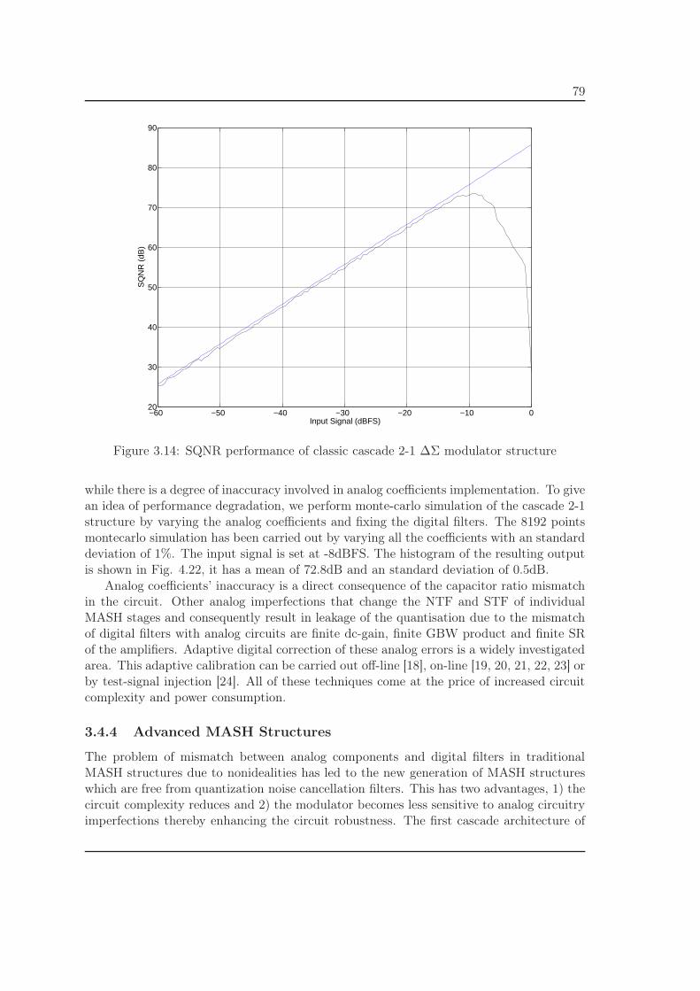
79
−60 −50 −40 −30 −20 −10 020
30
40
50
60
70
80
90
Input Signal (dBFS)
SQ
NR
(dB
)
Figure 3.14: SQNR performance of classic cascade 2-1 ∆Σ modulator structure
while there is a degree of inaccuracy involved in analog coefficients implementation. To givean idea of performance degradation, we perform monte-carlo simulation of the cascade 2-1structure by varying the analog coefficients and fixing the digital filters. The 8192 pointsmontecarlo simulation has been carried out by varying all the coefficients with an standarddeviation of 1%. The input signal is set at -8dBFS. The histogram of the resulting outputis shown in Fig. 4.22, it has a mean of 72.8dB and an standard deviation of 0.5dB.
Analog coefficients’ inaccuracy is a direct consequence of the capacitor ratio mismatchin the circuit. Other analog imperfections that change the NTF and STF of individualMASH stages and consequently result in leakage of the quantisation due to the mismatchof digital filters with analog circuits are finite dc-gain, finite GBW product and finite SRof the amplifiers. Adaptive digital correction of these analog errors is a widely investigatedarea. This adaptive calibration can be carried out off-line [18], on-line [19, 20, 21, 22, 23] orby test-signal injection [24]. All of these techniques come at the price of increased circuitcomplexity and power consumption.
3.4.4 Advanced MASH Structures
The problem of mismatch between analog components and digital filters in traditionalMASH structures due to nonidealities has led to the new generation of MASH structureswhich are free from quantization noise cancellation filters. This has two advantages, 1) thecircuit complexity reduces and 2) the modulator becomes less sensitive to analog circuitryimperfections thereby enhancing the circuit robustness. The first cascade architecture of

80 3. ∆Σ Modulator and System Level Modeling
69.5 70 70.5 71 71.5 72 72.5 73 73.5 74 74.50
100
200
300
400
500
600
700
SQNR (dB)
Num
ber
of o
ccur
renc
e
Mean=72.8dBStd. Deviation=.5dB
Figure 3.15: Classic cascade 2-1 architecture’s sensibility to analog and digital components’mismatches
this nature is presented in [25]. This structure is called multi-stage closed loop (MSCL).Every stage in this structure is a single-order modulator and a global feedback is introducedfrom the output, which is the sum of the output of all comparators. An enhanced versionof this structure is Generalized multi-stage closed loop (GMSCL) [15, 16]. This is basicallya cascade 2-2 structure, with each stage implemented as a feedforward structure, and aglobal feedback is used from the output. This structure is shown in Fig. 3.16.
Another such type of architecture is Sturdy MASH ∆Σ modulator presented in [17]and illustrated in Fig. 3.17.
Like GMSCL structure, the SMASH structure is less sensitive to opamp gain andcoefficient errors than the traditional MASH structure: finite opamp gain and coefficientmismatch will affect the zeros of the overall NTF, and the error will be suppressed by thesecond loop. This is because both STF and NTF are achieved by means of fully analogcomponents, in contrast with the traditional MASH structure in which digital filters formthe overall noise transfer function.
3.5 Multibit Modulators
With the expression for DR of an ideal Lth-order, B-bits internal quantizer ∆Σ modulatorgiven by:

81
−
−
DigitalOutput
DAC1
DAC2
DAC3
AnalogInput
−integrator integrator
integrator integrator
3
0.4 0.6
1
2
2
0.20.2
0.20.20.25
z−1
1−z−1z−1
1−z−1
z−1
1−z−1z−1
1−z−1
Figure 3.16: Generalized multi-stage closed loop (GMSCL)
DigitalOutput
integratorintegrator−−
integratorintegrator
AnalogInput
− − −
2
2
z−1
1−z−1
αz−1
1−z−1
E1
E2
E1
βz−1
1−z−1 Q1
z−1
1−z−1 Q2
Figure 3.17: Sturdy MASH (SMASH) structure
DR(dB) ≈ 10log10
[
3
2
(2L + 1)
π2LOSR2L+1(2B − 1)2
]
(3.37)

82 3. ∆Σ Modulator and System Level Modeling
it can be deduced that with each additional bit in the quantizer, 6dB of DR (equivalentto 1-bit resolution) is gained. Another advantage is the stable operation of the modulatorfor an increased range of signal levels [60]. As a general rule, the lower the resolution ofthe quantizer used, the more suspicious the designer should be about instability. There aretwo principal disadvantages of multibit quantizers: 1) The quantizer is realized generallyby flash ADC, whose complexity increases exponentially with the number of bits. Hencethis number can seldom exceed 4 or 5. 2) The nonlinearities caused by uneven spacingsof the DAC levels degrade the SNDR performance of the system. The filtering of thesenonlinearities is a highly researched domain, so a number of techniques have been proposedin the literature to counter them. These techniques can be broadly classified into analogcorrections and digital calibrations. In the analog domain, the most commonly used onesare element rotation (also called data-weighted averaging) [63, 64], individual level averag-ing [65], vector based mismatch shaping [66] and tree-structure element selection [67]. Allthese techniques use the unit-element DAC structure [60], but each uses a different strat-egy for the selection of the unit elements for a given digital input code. These techniquesflatten the nonlinearity of the multibit DAC into a pseudo-random noise and perform noise-shaping to reduce in-band noise power. Since these schemes rely on oversampling and noiseshaping, they are ineffective for low values of OSR, which is the case for wideband con-verters. Digital calibration techniques, on the other hand, acquire the DAC errors in adigital form, and then nullify their effects in the digital domain. These corrections can bemade just once at the power up of the circuit [68], or they can be run as a backgroundprocess during normal operation [69]. It can be noted that a multibit quantizer can beused in the second stage of a MASH structure without the need for any correction of itsDAC nonlinearity [70]. This is due to the fact that the second-stage output comprising itsDAC nonlinearity is multiplied by the NTF of first stage in the form of digital filter H2(z).Since this filter has a highpass characteristic, the nonlinearity error of the second-stageDAC is suppressed in the baseband. Another reason for insensitivity of MASH structureto second-stage DAC nonlineaity is that this stage processes only the quantization noiseof the first stage. And hence DAC nonlinearity of this stage does not generate any signalharmonic distortion, but only adds small noise, which is usually tolerable.
3.6 Continuous Time and Hybrid (Continuous Time/Discrete
Time) Modulators
The initial implementations of ∆Σ modulators used continuous-time (CT) loop filters [71],but with the advent of SC circuits, the focus has been shifted to DT loop filters. SCcircuits are attractive because they exhibit good accuracy and good linearity. In addition,the difference equations which describe an SC circuit are independent of the clock rate,and hence the transfer function of an SC circuit scales naturally with the clock frequency.In contrast, CT filters generally have inferior linearity and accuracy. The time-constantsof a CT filter are subject to large variation and furthermore do not track the clock rate.Consequently, the time-constants of a CT loop filter typically require calibration and thatcalibration is only valid for a single clock frequency. In addition, CT implementations are

83
highly sensitive to the clock jitter. Despite these disadvantages, the CT implementationsof ∆Σ modulator are gaining increasing interest for two important reasons:
1. CT modulators possess inherent anti-aliasing, with the degree of alias suppressionequivalent to the the degree of quantization-noise suppression [60]. Inherent anti-aliasing simplifies system design by eliminating the anti-alias filter, which typicallymust precede DT implementations. Inherent anti-aliasing also improves system per-formance, since it also eliminates the noise-folding associated with sampling the inputsignal. By using CT loop filter, the sampling of the signal takes place at the outputof the filter in contrast to the DT loop filter where sampling is done at the inputof the filter. Thus, imperfections of the sampling process, and the folding of thewideband noise, both take place at a much less sensitive point in the loop.
2. The theoretical limit on the clock rate of a CT modulator is determined by theregeneration time of the quantizer and the update rate of the feedback DAC, whereasin an SC modulator the clock rate is limited by the opamp settling requirements toabout 25% → 30% of the unity-gain frequency fu of the amplifiers within it. Inpractice, a CT modulator can operate with a clock frequency (and thus achievea signal bandwidth) which is 2-4 times greater than that which can be achievedwith SC techniques, but with a lower linearity and accuracy. The reason for thisincreased bandwidth is that the settling error in an SC stage depends exponentiallyon the fu/Fs ratio, and hence the error grows rapidly when this ratio drops belowabout 4. By contrast, the error introduced by opamp bandwidth in a CT modulatorincreases only gradually when fu/Fs is reduced. Recent CT modulators have achievedbandwidths of 10 MHz in 0.18- m CMOS technology [72], [73] and 15 MHz [74]and 20 MHz [75] in 0.13-µm CMOS technology, all with a resolution of 11 bits ormore. These results suggest that CT implementations are capable of operating atsignal bandwidths difficult to achieve with DT designs while still maintaining a highresolution.
These two advantages are driving the fresh interest for CT ∆Σ modulators with band-widths in the multi-MHz range. Some recent publications are using hybrid CT/DT solu-tions for A/D conversion that combine the benefits of CT and DT circuits, while minimizingthe problems associated with CT design. The hybrid solution presented in [76] uses cascade2-1 architecture shown in Fig. 3.18, where the second-order first stage is implemented inCT, while the first-order second stage is a DT circuit.
The first-stage is implemented completely as CT circuit to achieve the maximum anti-aliasing benefit of CT operation and to minimize the settling requirements for the first-stage sampling circuit. However, the second stage of the proposed cascaded modulatorcan be implemented as either a CT or a DT modulator without affecting noise shapingof the first-stage sampling error. Furthermore, because the output of the CT first stageis already a sampled-data signal, the antialiasing performance of the overall modulatoris the same for either a CT or DT second-stage implementation. Although a CT secondstage would provide the benefits of CT design, including slower, lower power amplifiers andimproved attenuation of second-stage sampling errors, there are several disadvantages to a

84 3. ∆Σ Modulator and System Level Modeling
Figure 3.18: Hybrid (CT/DT) ∆Σ modulator [76]
CT second stage. The first-stage sampling circuit would see a resistive input, requiring alow-output-impedance stage for the sampling circuit amplifier. Because this circuit is a SCcircuit operating at a high sampling rate, the first-stage sampling circuit amplifier must bea fast single-stage design, and therefore driving a resistive load would be difficult. A CTsecond stage would also require an additional feedback path to stabilize the loop againstexcess loop delay, adding to the implementation complexity. Moreover, the extra stabilizingpath would require an additional summing junction at the input of the quantizer, whichwould necessitate another amplifier and active sampling. This amplifier would operateas a DT circuit, negating the low-power amplifier benefit of a CT design. Because a CTimplementation of the second stage would likely require an additional sampling amplifier,a DT second stage implementation will dissipate approximately the same power as a CTimplementation. Furthermore, the first-stage sampling circuit driving a DT second stagewill see a capacitive, rather than resistive, load when driving a DT second stage. Althoughthe DT integrator amplifier will suffer incomplete settling because of the high samplingrate targeted in this research, those errors will be shaped by the second-order first stage,mitigating their impact on the overall modulator performance. For these reasons, andbecause a DT second stage would not affect the anti-aliasing performance of the modulator,a DT implementation was identified as the lowest power option for the second stage of themodulator.
3.7 System Level Modeling
System level modeling helps in determining the specifications of fundamental buildingblocks of ∆Σ modulator. It is the first step in the design of analog integrated circuits.Based on the results of system level modeling, a transistor-level design using sophisticatedtools like Cadence design suite is undertaken. For the purpose of system level modeling,

85
the classic Boser structure [12] is chosen. In this section, modeling is performed for clockjitter, switches’ thermal noise and opamp noise. Modeling at the level of opamp includessaturation, finite dc-gain, finite gain-bandwidth product and slew rate. Comparator non-idealities of dc-offset and hysteresis are also taken into account.
3.7.1 Clock Jitter
The operation of an SC circuit depends on complete charge transfers during each of theclock phases [77]. Once the analog signal has been sampled, the SC circuit is a sampled-datasystem where variations of the clock period have no direct effect on the circuit performance.Therefore, the effect of clock jitter on an SC circuit is completely described by computingits effect on the sampling of the input signal. This also means that the effect of clock jitteron a modulator is independent of the structure or order of the modulator. Clock jitterresults in a nonuniform sampling time sequence, and produces an error which increasesthe total error power at the quantizer output. The magnitude of this error is a functionof both the statistical properties of the jitter and the modulator input signal. The errorintroduced when a sinusoidal signal with amplitude A and frequency fin is sampled at aninstant which is in error by an amount δ is given by:
x(t + δ) − x(t) ≈ 2πfinδAcos(2πfint) = δd
dtx(t) (3.38)
This effect is simulated at behavioral level by taking the input sample at an instantwhich differs from the ideal instant by δ:
x[n] = x(nTs + δ) (3.39)
In the model, it is assumed that the sampling uncertainty δ is a Gaussian randomprocess with standard deviation ∆τ . Whether oversampling is helpful in reducing theerror introduced by the jitter depends on the nature of the jitter. Since we assume thejitter white, the resultant error has uniform power-spectral density (PSD) from 0 to Fs/2,with a total power of (2πfin∆τA)2/2. In this case, the total error power will be reducedby the oversampling ratio [12].
3.7.2 Switch and Op-Amp Noise
The most important noise sources affecting the operation of an SC ∆Σ modulator are thethermal noise associated to the sampling switches and the intrinsic noise of the operationalamplifiers. These effects can be successfully simulated at the behavioral level by using themodel of a “noisy” integrator [78] shown in Fig. 3.19. It includes the thermal noise of theswitches and op-amp noise. Each noise source and its relevant model will be described inthe following paragraphs.
3.7.2.1 Switch Thermal Noise
Thermal noise is caused by the random fluctuation of carriers due to thermal energy and ispresent even at equilibrium. Thermal noise has a white spectrum and wide band, limited

86 3. ∆Σ Modulator and System Level Modeling
Figure 3.19: Noisy integrator model [78]
only by the time constant of the switched capacitors or the bandwidth of the operationalamplifiers. Referring to the SC implementation of integrator shown in Fig. 3.22, thesampling capacitor Cs is in series with a switch, with finite resistance Ron, that periodicallyopens, thus sampling a noise voltage onto Cs.
The total noise power can be found by evaluating the integral [10]:
e2T =
∫
∞
0
4kTRon
1 + (2πfRonCs)2df =
kT
Cs(3.40)
where k is the Boltzmann’s constant,T the absolute temperature, and 4kTRon the noisepower spectral density associated with the switch on-resistance. The switch thermal noisevoltage eT (usually called kT/C noise) is then superimposed to the input voltage x(t)leading to
y(t) = [x(t) + eT (t)] b
=
[
x(t) +
√
kT
Csn(t)
]
b (3.41)
where n(t) denotes a Gaussian random process with unity standard deviation andb = Cs/Ci is the coefficient of the integrator. The integrators or resonators of an SC ∆Σmodulator may include more than one SC input branch, each contributing to the totalnoise power. Each branch has to be modeled with a separate noise source.
87
3.7.2.2 Op-amp Noise
The total noise voltage of the operational amplifier referred to the integrator input can bemodelled as an additive gaussian noise. In this model, only thermal noise is considered,while flicker noise and dc offset are neglected. Indeed, in low-pass modulators, flicker noiseand dc offset are typically canceled by means of auto-zero, correlated double sampling,or chopper stabilization techniques, while they are not important in highpass or bandpassarchitectures. The noise power can be evaluated through a transistor-level noise simulationof the complete integrator in the proper clock phase, including feedback, sampling and loadcapacitors. The resulting output referred noise PSD has to be integrated over the wholefrequency spectrum, eventually taking into account the degradation of the thermal noisePSD introduced by the auto-zero or correlated double sampling techniques [79], and thendivided by b2 in order to refer the obtained noise power to the integrator input; where b isthe integrator gain. It is important to note that only the contribution of the sampled noiseis considered, assuming that no continuous-time paths are present across the modulator(this is typically the case in SC modulators due to the presence of a latched quantizer).
3.7.3 Op-amp Non-Idealities
The ∆Σ modulator operation depends on the performance of integrators, which can be con-sidered as its major building blocks. The integrators are in turn dependent on the func-tioning of their own building blocks i-e op-amps. Operational amplifiers’ non-idealitiesincluding finite and nonlinear dc-gain, finite gain-bandwidth product (GBW) and finiteslew rate (SR) cause incomplete transfer of charge in the switched-capacitor (SC) im-plementation of integrators which is a major cause of performance degradation of ∆Σmodulators. Several articles in the literature have discussed these effects and establishedtheir behavioural models to study their effect on integrators [80, 78, 81], which form thebasis of traditional low-pass ∆Σ modulators. We will discuss each non-ideality separatelyin the following sections.
3.7.3.1 Saturation
Saturation of an opamp output is due to the limited voltage swing that it can provide.In the latest CMOS technologies, small values of voltage supplies make the opamp outputvoltage swing very limited. Excessive output excursions of integrators are undesirablebecause of saturation or voltage clipping at the output of op-amps comprising integrators;if the output voltage exceeds opamp’s output voltage swing, the clipping occurs whichmay also render the system unstable. Small output excursions of integrators are desirablealso because they minimize the opamp output swing requirement resulting in the designof an opamp with good values of other performance parameters like gain, bandwidth andconsumption. If an integrator has an output range which exceeds the quantization step,it will overload the comparator and render the system unstable. Thus output excursion isan important parameter to measure at system level. System level simulations have beencarried out using MATLAB to study the output excursions of both integrators in Bosermodulator. Ten sets of 1.1 × 214 = 18022 point simulations with each set at a random

88 3. ∆Σ Modulator and System Level Modeling
integrator initial state, have been carried out. The first 1638 points have been truncatedto remove the transient effects. The ten sets of histograms of have been averaged for finalresults. The input signal is a sinusoid with an amplitude of 0.4 normalized with respect toquantization step i-e -8dBFS (dB with reference to full scale). The system level simulationshave been performed with sampling frequency normalized to one and input signal frequencyof 0.5 − 6.7139e − 4 = 0.4993.
The histogram showing the output excursions of two integrators are presented in Fig.3.20
−1.5 −1 −0.5 0 0.5 1 1.50
20
40
60
80
100
120
140
160
180
200
Output voltage normalized wrt Vref
Num
ber
of o
ccur
ence
1st integrator
2nd integrator
Figure 3.20: Integrators’ output excursion at Vin=-8dBFS
The results presented in Fig. 3.20 show that the output excursions are more significantin the first integrator, which is expected since it processes the difference of the usefulsignal and the quantization noise directly; unlike the second integrator which processes thesignal after it has undergone an attenuation equal to the first integrator’s coefficient. Thesaturations voltage of operational amplifier is normally set by quantization step i-e thevoltage range −V ref ↔ V ref , but since first integrator’s excursion exceeds this range, wehave to design opamps with higher voltage swings, thus increase the power consumption,which can become significant in low-voltage technologies.
The second integrator’s excursion is less than the first one, and well inside the quanti-zation step and is thus easily realized.
From another point of view, simulations to model the op-amp saturation have beenperformed by clipping the integrator output at ±V ref . That is any output greater thanV ref has been forced to be at V ref and any output less than −V ref has been forced tobe at −V ref . The resulting simulation result is shown in Fig. 3.21:

89
−60 −50 −40 −30 −20 −10 00
10
20
30
40
50
60
Input Amplitude (dBFS)
SQ
NR
(dB
)
Boser modulator without clipping
Boser modulator with clipping
Figure 3.21: Plot of SNR Vs Input Signal in the presence of filter clipping at ±V ref
As expected, the structure is affected by output saturation since it has large excursions.As we increase the input sinusoid amplitude, the output excursion becomes larger andlarger and at one point becomes unstable because of clipping. Thus the first opamp has tobe designed with voltage swing higher than ±V ref to achieve a good SQNR performance.
3.7.3.2 Finite DC-Gain
An ideal delayed integrator with a gain b is described by z-domain transfer function:
Hideal(z) = bz−1
1 − z−1(3.42)
Although delay-less filters can be used to realize the desirable NTF, most often delayed-integrators are used in the first stage of the modulators as they are easily implemented inSC design. The operational amplifier finite open-loop dc-gain AO introduces errors in thisideal transfer function. This effect can be represented mathematically by:
Hpractical(z) = bαz−1
1 − βz−1(3.43)
where α and β are less-than-unity quantities and represent gain degradation and filterleakage (or gain and pole location perturbation)respectively. Gain degradation results inonly a fraction of the input signal being added to the output and filter leakage results inonly a fraction of the last output being added to the input.
To work out the values of α and β, let us take the standard SC implementation ofintegrator illustrated in Fig. 3.22:

90 3. ∆Σ Modulator and System Level Modeling
−
+
Sd T
Cs
Cp
Ci
Td S
vinvout
Figure 3.22: Integrator implementation in a SC circuit
Where Cp represents the input parasitic capacitance of the op-amp, parasitic capac-itance of the switches and the plates of capacitors connected to the negative input ofthe op-amp. Solving charge-transfer equations for this filter, keeping in view the charge-conservation law, the practical transfer function in terms of capacitances and op-ampdc-gain A0 is given by:
Hpractical(z) =Cs
Ci
A0
CsCi
+Cp
Ci+A0+1
z−1
1 −Cp
Ci+A0+1
CsCi
+Cp
Ci+A0+1
z−1
(3.44)
where Cs
Ci= b is the gain of the filter and Cp
Ci= p is the gain of the parasitic voltage.
Replacing these values in Eqn. 3.44:
Hpractical(z) = b
A0
b+p+A0+1z−1
1 − P+A0+1b+p+A0+1z−1
(3.45)
The value of b for the Boser modulator is 0.5, assuming a reasonable value of 0.01 forp, the exact transfer function of the first integrator turns out to be:
Hpractical(z) = 0.5A0
A0+1.51z−1
1 − A0+1.01A0+1.51z−1
(3.46)
Therefore the values of α and β are given by:
α =A0
A0 + 1.51, β =
A0 + 1.01
A0 + 1.51(3.47)
Using Eqn. 3.46 as the transfer function for the first integrater, the Boser modulatoris simulated at a range of values of A0 to identify the effect of this non-ideality. The inputsignal is a sinusoid at an amplitude of 0.4 normalized with respect to quantization step i-e-8dBFS at frequency of 0.4993fs. The simulation result is shown in Fig. 3.23:
This figure shows that the Boser architecture requires the 40dB op-amp dc-gain toattain the ideal SQNR performance.

91
10 15 20 25 30 35 40 45 50 55 6046
47
48
49
50
51
52
53
54
55
Op−amp dc−gain (dB)
SN
DR
(dB
)
Figure 3.23: SNR vs. Op-Amp DC-Gain
3.7.3.3 Finite Gain-Bandwidth Product and Slew Rate
Finite Gain-Bandwidth Product (GBW) and Slew Rate (SR) are responsible for incompleteor inaccurate charge transfer in SC circuits. In the case of integrator, finite GBW of theop-amp forces only a fixed fraction of the new charge in each charge transfer phase of theclock (T) to get stored in the integrating capacitor of the filter. This is due to the non-zero time constant, τ = (1 + b)/2πGBW as derived in Annex. A. The fact that in eachclock cycle there is a charge trasfer error which is proportional to the input of the filter,results in distortion at the output of the modulator. With the assumption of a single-polemodel for the op-amp, the output transient of the integrator during nth integration phaseis represented by:
vout(t) = βvout(nTs − Ts) + bαvin(1 − e−tτ ), 0 < t <
Ts
2(3.48)
where vout is the output of the integrator, Ts = 1/Fs is the sampling period, vin isthe input of the integrator and τ is the time constant of the op-amp which makes up theintegrator. If this integrator represents the first integrator of the Boser modulator, vin isgiven by:
vin = x(nTs − Ts/2) − y(nTs − Ts) (3.49)
where x is the input of the modulator and y is the output of the modulator. In caseof infinite GBW of the op-amp, τ falls to zero and Eqn. 3.48 reduces to Eqn. 3.43, whilethe values of α and β are given by Eqn. 3.47. Finite GBW on the other hand, reduces

92 3. ∆Σ Modulator and System Level Modeling
the gain of the filter which in turn reduces the value of the new input to be added to theoutput.
Slew rate of an op-amp is the maximum rate of voltage change that it can provide atits output. Unfortunately it is practically a finite quantity that is dependant on the biascurrent of the op-amp and its load capacitance:
SRs =Imax
CL(3.50)
where Imax is the maximum current that can be supplied by the op-amp and is equiv-alent to twice the bias current of a single branch of a differential implementation. CL isthe load capacitance on the op-amp during the integration phase and is composed of allthe capacitances connected to the op-amp during this phase. Eqn. 3.50 can be called theSR-supply by the op-amp. SR-demand on the other hand is characterised by maximumslope of the curve drawn by charge transfer eqn. 3.48. This curve finds it maximum slopeat t = 0, given by:
SRd =d
dtvout(t)|max =
bαvin
τ(3.51)
Now, two possibilities arise because of this supply and demand issue:
1. The value of SR-demand given by Eqn. 3.51 is lower than the value of SR-supply ofthe op-amp given by Eqn. 3.50. In this case, there is no SR limitation and the chargetransfer continues to function as specified by Eqn. 3.48 during the whole integrationphase (until t = Ts/2)
2. The second possibility is that the SR-demand of the charge transient exceeds the SR-supply of op-amp. In this case, the op-amp undergoes slewing and provides a linearcharge transfer in contrast to the exponential charge transfer given in Eqn. 3.48.It continues to supply constant current equivalent to its maximum current until thecurrent demand becomes lower than its maximum current (t < t0). This correspondsto a linear voltage change curve (having a constant slope). This maximum slope isthe SR-supply of the op-amp. This concept is illustrated graphically in Fig. 3.24.
The charge transfer transient can now be represented by Eqns:
vout(t) = βvout(nTs − Ts) + SRst, t ≤ t0 (3.52)
vout(t) = βvout(nTs − Ts) + (bαvin − SRst0) ∗ (1 − e−t−t0
τ ), t > t0 (3.53)
where SRst0 is the value reached by vout(t) at t = t0 where the limitation of SR endsi-e SRd equals SRs.
Imposing the condition for the continuity of the derivatives of Eqns. 3.52-3.53 in t0,we obtain:

93
0 0.1 0.2 0.3 0.4 0.5 0.6 0.7 0.8 0.9 1
0.2
0.4
0.6
0.8
1
1.2
1.4
Time (xTs sec)
Out
put V
olta
ge (V
)
Ideal Output
SR>2*pi*GBW
SR=1.4*GBW,slewing transition
SR=1.4*GBW,exponential transition
SR=1.1*GBW,slewing transition
SR=1.1*GBW,exponential transition
Charge transfer errors
Figure 3.24: Increase in settling error due to slew rate reduction
t0 =bαvin
SRs− τ (3.54)
If t0 > Ts/2 Eqn. 3.52 holds for the whole clock period. Otherwise, using the value oft0 from Eqn. 3.54 in Eqn. 3.53, we obtain:
vout(t) = βvout(nTs − Ts) + Vs − sgn(Vs)SRsτe−(Ts2τ
−|Vs|
SRsτ+1) (3.55)
where Vs is given by:
Vs = bαvin (3.56)
Finite SR supplied by the op-amp results in changing the gain of the integrator in anon-linear fashion and produces harmonics in the output degrading the SNDR. Simulationshave been performed for Boser architecture by varying the values of SRs and observingthe output SNDR at two different values of GBW. The result is illustrated in Fig. 3.25.
The results show that atleast a SRs of 1.8Fs(V/sec) is necessary to guarantee theoptimum SNDR.
3.7.4 Comparator Non-Idealities
The effect of the comparator non-idealities in the operation of the ∆Σ modulators is muchlower than those of the integrator because of the position that the comparator occupiesin the modulator loop. A possible input offset in the comparator when referred to themodulator input is attenuated by the DC gains of the integrators that precede it in the loop.
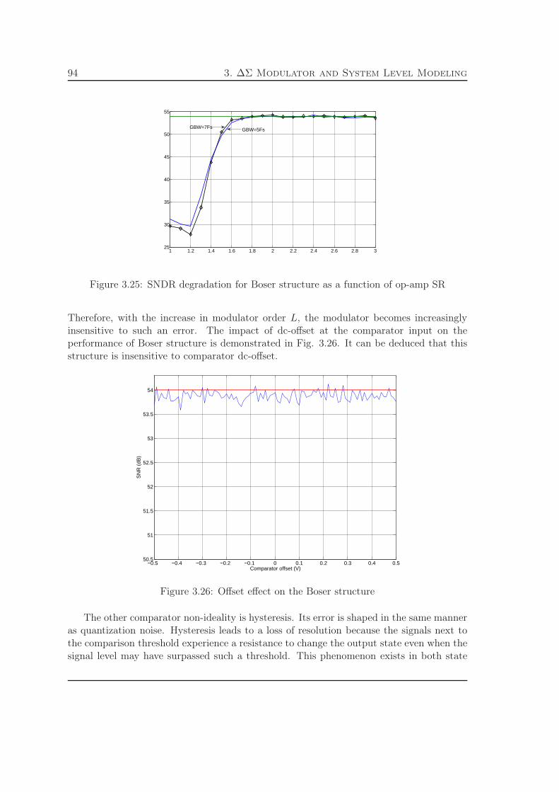
94 3. ∆Σ Modulator and System Level Modeling
1 1.2 1.4 1.6 1.8 2 2.2 2.4 2.6 2.8 325
30
35
40
45
50
55
GBW=5FsGBW=7Fs
Figure 3.25: SNDR degradation for Boser structure as a function of op-amp SR
Therefore, with the increase in modulator order L, the modulator becomes increasinglyinsensitive to such an error. The impact of dc-offset at the comparator input on theperformance of Boser structure is demonstrated in Fig. 3.26. It can be deduced that thisstructure is insensitive to comparator dc-offset.
−0.5 −0.4 −0.3 −0.2 −0.1 0 0.1 0.2 0.3 0.4 0.550.5
51
51.5
52
52.5
53
53.5
54
Comparator offset (V)
SN
R (
dB)
Figure 3.26: Offset effect on the Boser structure
The other comparator non-ideality is hysteresis. Its error is shaped in the same manneras quantization noise. Hysteresis leads to a loss of resolution because the signals next tothe comparison threshold experience a resistance to change the output state even when thesignal level may have surpassed such a threshold. This phenomenon exists in both state

95
changes generating a hysteresis cycle as illustrated in Fig. 3.27.
∆
h
Vo
Vi
Figure 3.27: Transfer curve of a comparator with hysteresis
It is due to the fact that the comparator has a memory of the previous state, so anoverdrive is necessary to make it commute to the correct state. The damage the hysteresisincurs on the performance of Boser structure is shown in Fig. 3.28.
0 0.05 0.1 0.15 0.2 0.25 0.3 0.35 0.4 0.45 0.544
45
46
47
48
49
50
51
52
53
54
55
Hysteresis (V)
SN
R (
dB)
Figure 3.28: Hysteresis impact on the performance of Boser structure
It is evident that hysteresis has a highly deteriorating effect on the performance. At

96 3. ∆Σ Modulator and System Level Modeling
hysteresis of 13% of full-scale, 3dB of resolution (equivalent to half bit) is lost. The outputspectrum showing increased inband noise due to hysteresis is exposed in Fig. 3.29.
10−5
10−4
10−3
10−2
10−1
100
−120
−100
−80
−60
−40
−20
0
20
40
Frequency (xFs Hz)
PS
D (
dB/H
z)
13% hysteresis
Ideal
Figure 3.29: Output spectrum in presence of Hysteresis
In addition to this type of hysteresis, which is deterministic, there is another of randomnature. It is a typical error of the latched comparators with a reset phase during whichthe memory of the previous state must be fully erased. Due to the deficiencies of the realdevices, this process leaves certain residues of the previous state, leading to an uncertaintyzone. In this zone the output of the comparator is not determined only by its input, butin addition, by the previous state and the transitions of the signals resetting the latch. In[12], it is shown that in an Lth-order modulator, the inband power of the error due to thecomparator hysteresis can be approximated by Ph = 4h2π2L/[(2L + 1)M (2L+1)].
3.8 Conclusion
In this chapter, the principle of ∆Σ modulator has been presented. The state-of-art second-order topologies are presented. Since second-order modulator does not provide the requiredconversion performance, two broad classifications of higher-order configurations namelysingle-loop and multi-stage or MASH topologies are elaborated. Some latest versions ofMASH topologies which are free from noise-leakage or mismatch problems are also illus-trated. System level modeling is carried out on Boser structure for circuit level parameterslike op-amp dc-gain, gain-bandwidth-product, slew rate etc. This helps in finding thespecifications of the main building blocks like op-amp and comparator. It is found thatan op-amp with ±1.3V ref voltage-swing, 40dB dc-gain, 5Fs GBW product and 1.8Fs SRwill provide the near-to-ideal performance.

97
Chapter 4
High-Pass ∆Σ Modulator
4.1 Introduction
The traditional low-pass ∆Σ modulation, described in the preceding chapter, can performa very good job if the inherent circuit noises are ignored. In practice, however, the circuitlow frequency noise such as flicker noise, offset voltage of the op-amp (offset noise) andclock feedthrough noise, always exists and degrades the performance of the ∆Σ modula-tors seriously. Two major techniques, namely the correlated double sampling [82, 83] andchopper stabilization [83, 84, 85] have been proposed and applied to the operational am-plifier (op-amp). These solutions, however, have not achieved a significant noise reductionand the performance still remains degraded. A new design technique to counter the low-frequency noise problem has been proposed in [6] which is called high-pass ∆Σ modulator.In this architecture, the chopper stabilization technique is applied to the ∆Σ modulatorrather than to the op-amp to mitigate the noise efficiently.
In this chapter, the principle of high-pass ∆Σ modulation is explained, its traditionalarchitecture is exposed and a new architecture is proposed. The performances of thesestructures are compared in the presence of op-amp non-idealities. Then the cascadedversion of high-pass modulator is discussed and a novel technique is presented. In the end,the latest generation of cascaded structures i-e multi stage closed loop is explained and isapplied to high pass modulators.
4.2 Principle
The working principle of high-pass (HP) ∆Σ modulator is the same as that of low-pass(LP) ∆Σ modulator, i.e. the quantization noise is shaped away from the signal band bya loop filter. The difference lies in the placement of the signal band. In the case of HP∆Σ modulator, it is located at Fs/2, where Fs is the sampling frequency, compared witha pass-band at dc for the LP ∆Σ modulator. Thus, the transformation of a low-pass tohigh-pass modulator is a high-pass to low-pass transformation for the quantization noisetransfer function. It is also the low frequency to high frequency transformation for a signal.This transformation makes the HP ∆Σ modulator completely immune to low frequency
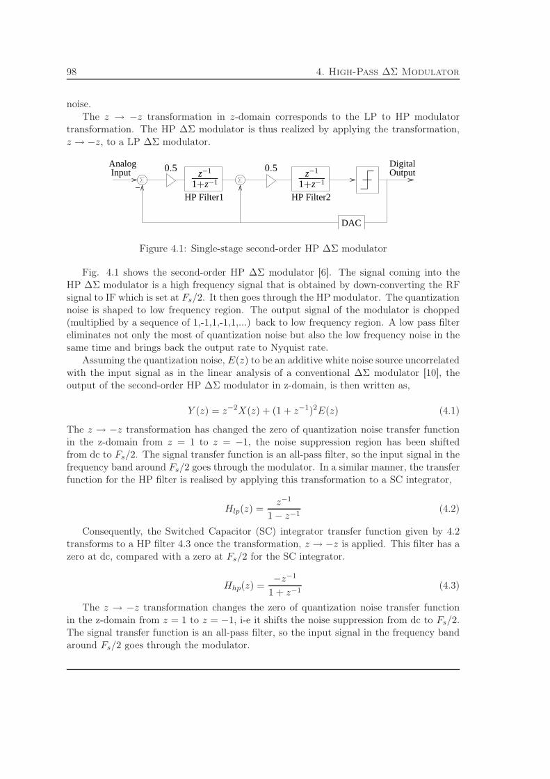
98 4. High-Pass ∆Σ Modulator
noise.The z → −z transformation in z-domain corresponds to the LP to HP modulator
transformation. The HP ∆Σ modulator is thus realized by applying the transformation,z → −z, to a LP ∆Σ modulator.
Input Output
−
Analog Digital
DAC
HP Filter1 HP Filter2
z−1
1+z−1
0.5 0.5 z−1
1+z−1
Figure 4.1: Single-stage second-order HP ∆Σ modulator
Fig. 4.1 shows the second-order HP ∆Σ modulator [6]. The signal coming into theHP ∆Σ modulator is a high frequency signal that is obtained by down-converting the RFsignal to IF which is set at Fs/2. It then goes through the HP modulator. The quantizationnoise is shaped to low frequency region. The output signal of the modulator is chopped(multiplied by a sequence of 1,-1,1,-1,1,...) back to low frequency region. A low pass filtereliminates not only the most of quantization noise but also the low frequency noise in thesame time and brings back the output rate to Nyquist rate.
Assuming the quantization noise, E(z) to be an additive white noise source uncorrelatedwith the input signal as in the linear analysis of a conventional ∆Σ modulator [10], theoutput of the second-order HP ∆Σ modulator in z-domain, is then written as,
Y (z) = z−2X(z) + (1 + z−1)2E(z) (4.1)
The z → −z transformation has changed the zero of quantization noise transfer functionin the z-domain from z = 1 to z = −1, the noise suppression region has been shiftedfrom dc to Fs/2. The signal transfer function is an all-pass filter, so the input signal in thefrequency band around Fs/2 goes through the modulator. In a similar manner, the transferfunction for the HP filter is realised by applying this transformation to a SC integrator,
Hlp(z) =z−1
1 − z−1(4.2)
Consequently, the Switched Capacitor (SC) integrator transfer function given by 4.2transforms to a HP filter 4.3 once the transformation, z → −z is applied. This filter has azero at dc, compared with a zero at Fs/2 for the SC integrator.
Hhp(z) =−z−1
1 + z−1(4.3)
The z → −z transformation changes the zero of quantization noise transfer functionin the z-domain from z = 1 to z = −1, i-e it shifts the noise suppression from dc to Fs/2.The signal transfer function is an all-pass filter, so the input signal in the frequency bandaround Fs/2 goes through the modulator.

99
The dynamic range of a HP ∆Σ modulator can be estimated in the same manner as thatof a LP modulator. The result is that the HP modulator provides the same performanceas the LP modulator. For a generalized Lth order HP modulator, L+ 1/2 bit of resolutionis gained for every doubling of the oversampling ratio. Moreover, the quantization noisebeing shaped out to baseband, it completely covers the low frequency noise such as 1/fnoise, and offset has no effect on the performance of the HP modulator, which is not thecase in a LP modulator.
4.3 Single-Loop HP ∆Σ Modulator Structures
4.3.1 Boser-based Structure
A classical structure of HP modulator is presented in [6]. It is obtained by applying z → −ztransformation to the LP second-order modulator proposed by Bernard E. Boser in [12]and presented in Sec. 3.3.1 on Page 68. This HP modulator is shown in Fig. 4.1.
The linear analysis of this structure, performed on the same lines as for its LP coun-terpart, results in the STF of:
STF =0.25Gz−2
D(z−1)(4.4)
and the noise transfer function (NTF) is calculated to be:
NTF =(1 + z−1)2
D(z−1)(4.5)
where G is the quantizer gain and,
D(z−1) = 1 + (2 − 0.5G)z−1 + (1 − 0.25G)z−2
In classical literature, value of quantizer gain is assumed to be 4, which results in thefamous STF of:
STF = z−2 (4.6)
and NTF of:
NTF = (1 + z−1)2 (4.7)
Note that STF is an all pass filter and NTF is a low pass filter having a zero at Fs/2thus rejecting all the noise around signal band. A brief description of the advantages anddisadvantages of Boser structure is given in Sec. 3.3.1.

100 4. High-Pass ∆Σ Modulator
DAC
OutputDigital
high passfilter
high pass filterAnalogInput
−
z−1
1+z−1
−2/4
1/4
z−1
1+z−1
1/4
Figure 4.2: Silva-based Structure for High Pass ∆Σ Modulator
DAC
−
AnalogInput Output
−
Digital
HP Filter2HP Filter1
4/9
1/9
0.50.5
4/9
z−1
1+z−1z−1
1+z−1
Figure 4.3: Optimized version of Silva-based Structure
4.3.2 Silva-based Structure
Silva structure is presented in Sec. 3.3.2 on Page 70. This topology, adapted for high-passoperation, is shown in Fig. 4.2
The refined version of this low-distortion architecture with optimized coefficients ispresented in [55] for low-pass operation. Its high-pass version is shown in Fig. 4.3.
The linear analysis of this optimized architecture gives an STF of:
STF =G/9
D(z−1)(4.8)
and the NTF of:
NTF =(1 + z−1)2
D(z−1)(4.9)
where G is the quantizer gain and,
D(z−1) = 1 + (2 − 2G
9)z−1 + (1 − G
9)z−2
Assuming a value of 9 for G results in:
STF = 1, NTF = (1 + z−1)2 (4.10)
The consequence of unity STF is that the input signal is cancelled out at the input offirst high pass filter/mirrored integrator and therefore the linearity requirements of the op-

101
amp constituting this filter are relaxed. The disadvantages of Silva structure are discussedin Sec. 3.3.2.2.
4.3.3 Oberst-based Structure
The state-of-the-art in the series of second-order ∆Σ modulator topologies is Oberst struc-ture [14], which is discussed in 3.3.3 on Page 71. The high-pass version of this structure isillustrated in Fig. 4.4.
OutputDigital
DAC
AnalogInput
HP Filter2
HP Filter1
−
0.5 0.5
0.25
0.25z−1
z−1
1+z−11
1+z−1
Figure 4.4: Oberst-based Structure for High Pass ∆Σ Modulator
For an information on the benefits brought by this architecture and its inherent prob-lems, please refer to Sec. 3.3.3.
4.3.4 Proposed Unity-STF Structure
A new unity-STF structure has been proposed which mitigates the shortcomings of theexisting modulator architectures. This topology for high-pass conversion is shown in Fig.4.5. This is a mixed feedback feedforward structure in which the signal attacks the com-parator directly. The useful signal is cancelled at the input of both high-pass filters. Thusthe problem of second opamp distorting the useful signal, associated with the Oberst-basedarchitecture, has been addressed. Both the high-pass filters are implemented as delayedfilters, thus eliminating the issue of increased loading on opamp implementing the firsthigh-pass filter, which is not the case in Oberst-based structure. The issues related toSilva-based topology have been resolved by changing the auxiliary feedforward path fromaround the second high-pass filter to around the first high-pass filter as shown in the Fig.4.5.
This relaxes the requirements on the adder since there are only two branches to addas opposed to three branches in Silva-based structure. Implementing this adder as passiveadder, now results in lesser attenuation of the signal thus reducing the design requirementsof the quantizer. The loading on the first opamp has also been reduced as there is nofeedforward capacitor to charge.
4.3.4.1 Linear Analysis
As did earlier for Boser-based and Silva-based structures, replacing the quantizer by itslinear model shown in Fig. 3.5 and performing the analysis results in an STF of:
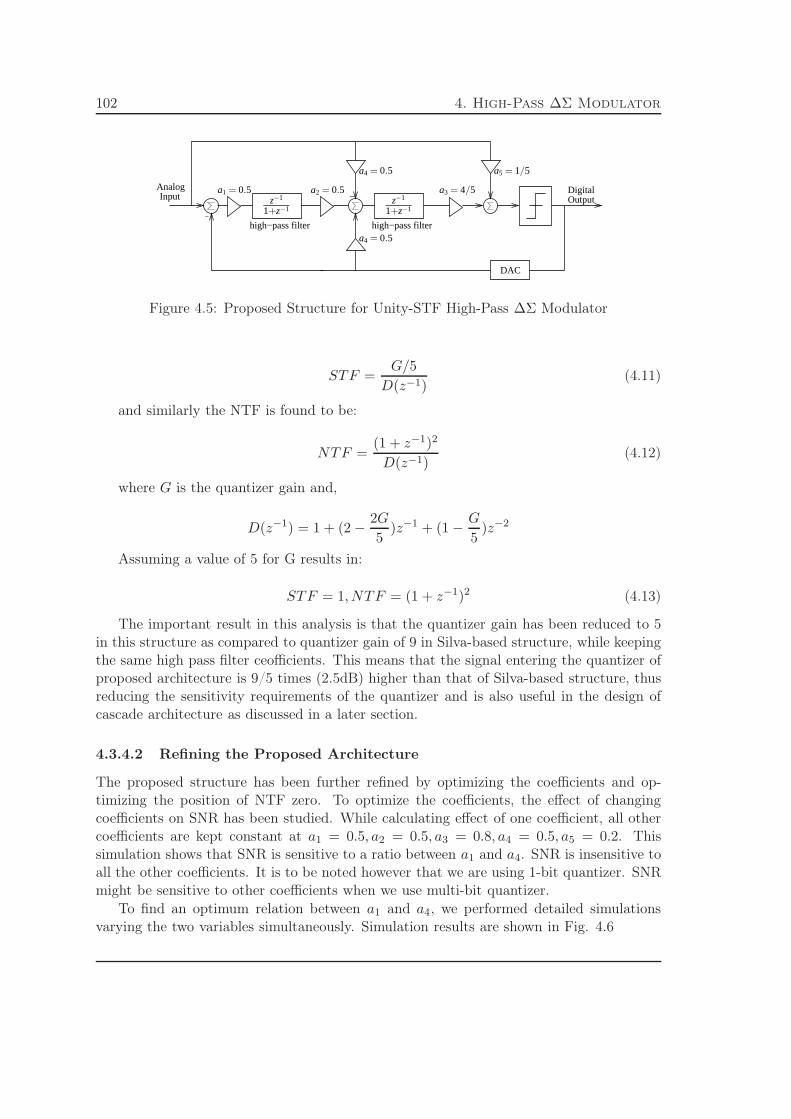
102 4. High-Pass ∆Σ Modulator
−
−
OutputDigitalAnalog
Input
DAC
high−pass filter high−pass filter
z−1
1+z−1z−1
1+z−1
a4 = 0.5
a3 = 4/5
a5 = 1/5
a1 = 0.5 a2 = 0.5
a4 = 0.5
Figure 4.5: Proposed Structure for Unity-STF High-Pass ∆Σ Modulator
STF =G/5
D(z−1)(4.11)
and similarly the NTF is found to be:
NTF =(1 + z−1)2
D(z−1)(4.12)
where G is the quantizer gain and,
D(z−1) = 1 + (2 − 2G
5)z−1 + (1 − G
5)z−2
Assuming a value of 5 for G results in:
STF = 1, NTF = (1 + z−1)2 (4.13)
The important result in this analysis is that the quantizer gain has been reduced to 5in this structure as compared to quantizer gain of 9 in Silva-based structure, while keepingthe same high pass filter ceofficients. This means that the signal entering the quantizer ofproposed architecture is 9/5 times (2.5dB) higher than that of Silva-based structure, thusreducing the sensitivity requirements of the quantizer and is also useful in the design ofcascade architecture as discussed in a later section.
4.3.4.2 Refining the Proposed Architecture
The proposed structure has been further refined by optimizing the coefficients and op-timizing the position of NTF zero. To optimize the coefficients, the effect of changingcoefficients on SNR has been studied. While calculating effect of one coefficient, all othercoefficients are kept constant at a1 = 0.5, a2 = 0.5, a3 = 0.8, a4 = 0.5, a5 = 0.2. Thissimulation shows that SNR is sensitive to a ratio between a1 and a4. SNR is insensitive toall the other coefficients. It is to be noted however that we are using 1-bit quantizer. SNRmight be sensitive to other coefficients when we use multi-bit quantizer.
To find an optimum relation between a1 and a4, we performed detailed simulationsvarying the two variables simultaneously. Simulation results are shown in Fig. 4.6

103
0.1 0.2 0.3 0.4 0.5 0.6 0.7 0.8 0.9 100.20.40.60.81
20
25
30
35
40
45
50
55
60
a1
X: 0.5Y: 0.55Z: 56.22
a4
SQN
R(d
B)
Figure 4.6: Coefficient Sweeping for Proposed Architecture
Results show that the ratio of a4/a1 = 1.1 gives the best SNR. We further confirmedthis result by carrying out the simulation at multiple input signal amplitudes and comparedthe classic relation a4/a1 = 1 with the newly found relation a4/a1 = 1.1. Results are shownin Fig. 4.7
These results show that we gain in highest achieved SNR with the new coefficients atthe cost of losing in SNR at low amplitudes.
The second step in refining the proposed modulator consists of placing the complexconjugate pair of zeros at a frequency fo near Fs/2 and inside the signal band whichminimizes the inband quantisation-noise power. The generalized NTF having a notch atfrequency fo is represented mathematically by:
NTF (z) = 1 + δz−1 + z−2 (4.14)
which in the frequency domain is:
NTF (f) = NTF (z)|z=2πf/Fs= 1 + δe−2πf/Fs + e−4πf/Fs (4.15)
where δ = 2cos(2πfo/Fs). It is a low pass filter with a notch at frequency fo. Notethat using the traditional value of fo at Fs/2, we get the standard NTF of second orderHP modulator. To find the optimum value of δ which results in the minimum inbandquantization noise, and thus the maximum signal to quantization noise ratio (SQNR), wehave to find the minimum of the function relating the inband noise power to the notchfrequency fo. Under the additive white noise model, the power of the quantization noiseis ∆2/12, and is uniformly distributed in the sampling bandwidth. Therefore, the powerspectral density of the shaped quantization noise is:
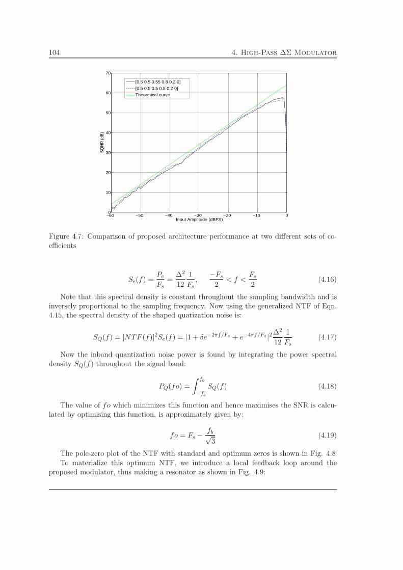
104 4. High-Pass ∆Σ Modulator
−60 −50 −40 −30 −20 −10 00
10
20
30
40
50
60
70
Input Amplitude (dBFS)
SQ
NR
(dB
)
[0.5 0.5 0.55 0.8 0.2 0]
[0.5 0.5 0.5 0.8 0.2 0]
Theoretical curve
Figure 4.7: Comparison of proposed architecture performance at two different sets of co-efficients
Se(f) =Pe
Fs=
∆2
12
1
Fs,
−Fs
2< f <
Fs
2(4.16)
Note that this spectral density is constant throughout the sampling bandwidth and isinversely proportional to the sampling frequency. Now using the generalized NTF of Eqn.4.15, the spectral density of the shaped quatization noise is:
SQ(f) = |NTF (f)|2Se(f) = |1 + δe−2πf/Fs + e−4πf/Fs |2 ∆2
12
1
Fs(4.17)
Now the inband quantization noise power is found by integrating the power spectraldensity SQ(f) throughout the signal band:
PQ(fo) =
∫ fb
−fb
SQ(f) (4.18)
The value of fo which minimizes this function and hence maximises the SNR is calcu-lated by optimising this function, is approximately given by:
fo = Fs −fb√3
(4.19)
The pole-zero plot of the NTF with standard and optimum zeros is shown in Fig. 4.8To materialize this optimum NTF, we introduce a local feedback loop around the
proposed modulator, thus making a resonator as shown in Fig. 4.9:

105
Re(z)
Im(z)
fs
2 −fB√3
fs
2 + fB√3
fs
2 + fB
fs
2 − fB
fs
2 dc, fs
Figure 4.8: Pole Zero Plot of NTF with Standard and Optimum Set of Zeros
−
InputAnalog
−
− OutputDigital
DAC
high passfilter
high passfilter
z−1
1+z−1z−1
1+z−1
0.5
0.007
0.5 0.5 4/5
1/5
Figure 4.9: A new second-order low-distortion high-SNR HP modulator
The simulation result showing the modulator output spectrum indicative of zero-displacement by adding a local feedback path is shown in Fig. 4.10:
This zero-optimization of the NTF gives us an SQNR improvement of 3.5dB [10] andis presented in simulation result in Fig. 4.11:
4.4 Comparative Analysis of Single-Loop HP Modulators
We presented various second-order HP ∆Σ architectures and discussed their pros and constheoretically in the preceding sections. In this section, we present a more in-depth analysisbacked with simulation results to analyse these architectures critically. We compare thefour architectures (Boser-based, Silva-based, Oberst-based, Proposed) on the basis of 1)

106 4. High-Pass ∆Σ Modulator
10−5
10−4
10−3
10−2
10−1
100
−100
−90
−80
−70
−60
−50
−40
−30
−20
−10
0
Frequency (xFs Hz)
PS
D (d
B/H
z)
Figure 4.10: Displaced Zero of the High Pass ∆Σ Modulator as a Result of Local Feedback
−60 −50 −40 −30 −20 −10 00
10
20
30
40
50
60
70
Input Amplitude (dBFS)
SQ
NR
(dB
)
Zero−displaced curve
Zero at Fs/2
Theoretical curve for zero−displaced
Figure 4.11: Performance improvement of Porposed Architecture by adding a Local Feed-back Loop
High-Pass Filter Output Excursions 2) Op-Amp Non-Idealities Effect. Excursions of the-high pass filters are an important parameter for comparison because they are directlyrelated to the voltage swing of the op-amps implementing the high-pass filters. We want
107
to keep these excursions to a minimal level to simplify the design of the op-amps. Otherop-amp non-idealities i-e finite dc-gain, finite unity-gain bandwidth and finite slew-rateeffect depend on the modulator architecture and the signal flow in the topology. The moreimmune the architecture is towards these non-idealities, the better the architecture.
The four modulator architectures with their coefficient values, used for comparisonanalysis are shown in Fig. 4.12:
Note that local feedback loop for zero-optimization has been removed from the proposedarchitecture so that it becomes comparable with other structures.
4.4.1 High-Pass Filter Output Excursion
System level simulations have been carried out using matlab to study the output excursionsof high-pass filters of different HP modulator schemes. The best scheme is one which hasminimum output range since it necessitates an opamp with the least voltage swing. Thedesign of an opamp becomes fairly easy, if the constraint of voltage swing is relaxed andit allows us to design opamp with good values of other performance parameters like gain,bandwidth and consumption. On the other hand, if a filter has an output range whichexceeds the quantization step, it will overload the comparator and render the systemunstable. Another phenomena which makes excessive output excursions undesirable isvoltage clipping at the output of op-amp; if the output voltage exceeds opamp’s outputvoltage swing, the clipping occurs which also renders the system unstable. Thus outputexcursion is an important parameter to compare the various modulator achitectures.
Like in the previous chapter, for each structure, ten sets of 1.1 × 214 = 18022 pointsimulations with each set at a random high-pass filter initial state, have been carried out.The first 1638 points have been truncated to remove the transient effects. The ten setsof histograms have been averaged for final results. The input signal is a sinusoid withan amplitude of 0.4 normalized with respect to quantization step i-e -8dBFS (dB withreference to full scale). The system level simulations have been performed with samplingfrequency normalized to one and input signal frequency of Fs/2 − 6.7139e − 04 = 0.4993.
The histograms showing the output excursions of two high-pass filters in the four com-peting topologies are presented in Fig. 4.13
The results presented in Fig. 4.13 show that the Boser-based structure has the highestexcursions in the first filter, which is expected since it processes both the useful signal andthe quantization noise. All the other structures have the same excursions for first high-passfilter since they all process just the shaped quantization noise. These excursions are wellinside the range −V ref ↔ V ref i-e the quantization step and are easily implementable.The saturations voltage of operational amplifier is normally set by quantization step i-ethe voltage range −V ref ↔ V ref , but since Boser-based structure’s excursion exceedsthis range, we have to design opamps with higher voltage swings, thus increase the powerconsumption, which can become significant in low-voltage technologies.
The second high-pass filter’s excursion is very less for Silva-based structure, the secondin the run is the Proposed architecture, then the Oberst-based and Boser-based structures.But all of them are well inside the quantization step and are thus easily realized.
From another point of view, we have performed simulations by modelling the op-amp
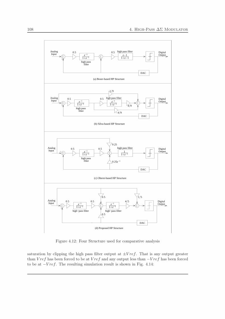
108 4. High-Pass ∆Σ Modulator
OutputAnalogInput
Digital
DAC
high passfilter
high pass filter
−
OutputDigital
DAC
high passfilter
high pass filterAnalogInput −
−
OutputDigitalAnalog
Input
DAC
high−pass filter high−pass filter
−
DAC
OutputAnalogInput
Digital
high passfilter
high pass filter
−
(a) Boser-based HP Structure
0.5 0.5z−1
1+z−1z−1
1+z−1
(c) Oberst-based HP Structure
0.5 0.5
0.25
0.25z−1
z−1
1+z−11
1+z−1
z−1
1+z−1z−1
1+z−1
0.5
(d) Proposed HP Structure
0.5 1/5
0.5 0.5 4/5
z−1
1+z−1
0.50.5
−4/9
4/9
1/9
z−1
1+z−1
(b) Silva-based HP Structure
Figure 4.12: Four Structure used for comparative analysis
saturation by clipping the high pass filter output at ±V ref . That is any output greaterthan V ref has been forced to be at V ref and any output less than −V ref has been forcedto be at −V ref . The resulting simulation result is shown in Fig. 4.14:

109
−1.5 −1 −0.5 0 0.5 1 1.50
50
100
150
200
First High Pass Filter Output Voltage Normalized wrt Vref
Num
ber o
f Occ
uren
ce
−1.5 −1 −0.5 0 0.5 1 1.50
100
200
300
400
Second High Pass Filter Output Voltage Normalized wrt Vref
Num
ber o
f Occ
uren
ce
Proposed
Silva−based
Oberst−based
Boser−based
Proposed
Silva−based
Oberst−based
Boser−based
Figure 4.13: Comparison of High-Pass Filters’ Output Excursion at Vin=-8dBFS
−60 −50 −40 −30 −20 −10 00
10
20
30
40
50
60
70
Input Amplitude (dBFS)
SQ
NR
(dB
)
Op−Amp Clipping at VREF
Proposed Structure
Oberst−based Structure
Silva−based Structure
Boser−based Structure
Theoretical Curve
Figure 4.14: Plot of SNR Vs Input Signal in the presence of filter clipping at ±V ref
As expected, the Boser-based structure is most affected by output clipping since it hasthe largest excursions. As we increase the input sinusoid amplitude, the output excursionbecomes larger and larger and at one point becomes unstable because of clipping.

110 4. High-Pass ∆Σ Modulator
4.4.2 Op-Amp Non-Idealities Effect
Analogous to the role of integrator in the traditional low-pass ∆Σ modulators is the roleof high-pass filter in HP ∆Σ modulator i-e it is its major building block. The perfor-mance of high-pass filter is directly related to the performance provided by its op-amp.Operational amplifiers’ non-idealities including finite and nonlinear dc-gain, finite gain-bandwidth product (GBW) and finite slew rate (SR) cause incomplete transfer of chargein the switched-capacitor (SC) implementation of high-pass filter which is a major causeof performance degradation of HP ∆Σ modulators. Several articles in the literature havediscussed these effects and established their behavioural models to study their effect onintegrators [80, 78, 81], which form the basis of traditional low-pass (LP) ∆Σ modulators.Here, we discuss the op-amp nonidealities effect on a high-pass-filter and compare the dif-ferent architectures discussed in the preceding sections with respect to their immunity tothese non-idealities. We will discuss each non-ideality separately in the following sections.
4.4.2.1 Finite DC-Gain
An ideal delayed high-pass filter with a coefficient b is described by z-domain transferfunction:
Hideal(z) = bz−1
1 + z−1(4.20)
Although delay-less filters can be used to realize the desirable NTF, most often delayed-integrators are used in the first stage of the modulators as they are easily implemented inSC design. The operational amplifier finite open-loop dc-gain AO introduces errors in thisideal transfer function. This effect can be represented mathematically by:
Hpractical(z) = bαz−1
1 + βz−1(4.21)
where α and β are less-than-unity quantities and represent gain degradation and filterleakage (or gain and pole location perturbation)respectively. Gain degradation results inonly a fraction of the input signal being added to the output and filter leakage results inonly a fraction of the last output being subtracted from the input. Since both the terms ofsubtraction are reduced, the output of high pass filter is less affected due to finite op-ampdc-gain. This is why, the high-pass filter is less prone to performance degradation due tofinite op-amp dc-gain than an integrator.
To work out the values of α and β, let us take the standard SC implementation offirst high-pass filter of the second-order HP ∆Σ modulators discussed previously. Thisimplementation is illustrated in Fig. 4.15.
Where Cp represents the input parasitic capacitance of the op-amp, parasitic capaci-tance of the switches connected to the negative input of the op-amp and parasitic capac-itance associated with the plates of capacitors connected to the negative input of theop-amp. Solving charge-transfer equations for this filter, keeping in view the charge-conservation law, the practical transfer function in terms of capacitances and op-ampdc-gain A0 is given by:

111
−
+
−1
T STd
Sd T
S
Sd Td
C1
C2
CP
A0
2×C2
vout
vin
Figure 4.15: First High-Pass Filter Implementation (standard) of a second-order HP ∆Σmodulator
Hpractical(z) =Cs
Ci
A0
CsCi
+Cp
Ci+A0+3
z−1
1 +Cp
Ci+A0−1
CsCi
+Cp
Ci+A0+3
z−1
(4.22)
where Cs
Ci= b is the gain of the filter and Cp
Ci= p is the gain of the parasitic voltage.
Replacing these values in Eqn. 4.22:
Hpractical(z) = b
A0
b+p+A0+3z−1
1 + p+A0−1b+p+A0+3z−1
(4.23)
The value of b for all the modulators is 0.5, assuming a reasonable value of 0.01 for p,the exact transfer function of the first high-pass filter turns out to be:
Hpractical(z) = 0.5A0
A0+3.51z−1
1 + A0−0.99A0+3.51z−1
(4.24)
Therefore the values of α and β are given by:
α =A0
A0 + 3.51, β =
A0 − 0.99
A0 + 3.51(4.25)
Using Eqn. 4.24 as the transfer function for the first high-pass filter, all the modulatorarchitectures discussed earlier have been simulated at a range of values of A0 to comparethe effect of this non-ideality on different architectures. The input signal is a sinusoid atan amplitude of 0.4 normalized with respect to quantization step i-e -8dBFS at frequencyof 0.4993Fs. The simulation result is shown in Fig. 4.16:
This figure shows that all the architectures require the op-amp with the DC Gainof 45-dB to acquire the signal to quantization noise ratio (SQNR) for the fixed inputamplitude. It can be observed that the proposed architecture is more robust than theother architectures in the presence of weak DC-Gain opamp.

112 4. High-Pass ∆Σ Modulator
0 10 20 30 40 50 6010
15
20
25
30
35
40
45
50
55
Op−Amp DC Gain (dB)
SN
DR
(d
B)
Vin=−8dBFS, OSR=32
Proposed structure
Oberst−based structure
Silva−based structure
Boser−based structure
Ideal op−amp
Figure 4.16: SNR Vs Op-Amp DC-Gain
4.4.2.2 Finite Gain-Bandwidth Product and Slew Rate
With the assumption of a single-pole model for the op-amp, the output transient of thehigh-pass filter during nth integration phase is represented by:
vout(t) = vout(nTs − Ts) + (−(1 + β)vout(nTs − Ts) + bαvin) ×(
1 − e−tτ
)
, 0 < t <Ts
2(4.26)
where vout is the output of the filter, Ts = 1/Fs is the sampling period, vin is the inputof the filter and τ = (3 + b)/2πGBW is the time constant of the op-amp comprising thefilter. The value of the time-constant τ is derived in the Annex. B. If this high-pass filterrepresents the first high-pass filter of a second-order modulator, vin is given by:
vin = x(nTs − Ts/2) − y(nTs − Ts) (4.27)
where x is the input of the modulator and y is the output of the modulator. In caseof infinite GBW of the op-amp, τ falls to zero and Eqn. 4.26 reduces to Eqn. 4.21, whilethe values of α and β are given by Eqn. 4.25. Finite GBW on the other hand, reducesthe gain of the filter which in turn reduces the value of the new input to be added to theoutput and also diminishes the value of the signal stored in the feedback capacitor whichhas to be added to the output during the integration phase.
A theoretical description of the op-amp slew rate is provided in the preceding chapter.In this chapter, we use those concepts to figure out the charge-transfer transient of high-pass filter in the presence of finite SR op-amp. SR demand on the op-amp is characterised
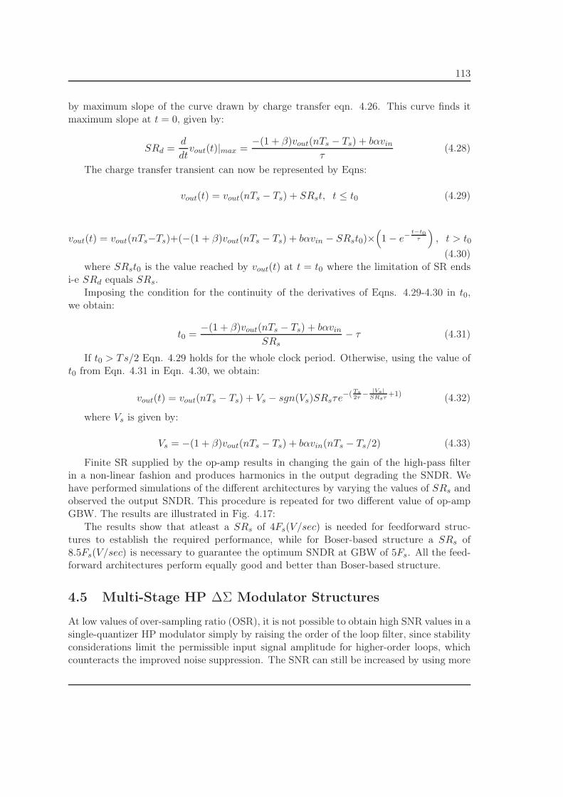
113
by maximum slope of the curve drawn by charge transfer eqn. 4.26. This curve finds itmaximum slope at t = 0, given by:
SRd =d
dtvout(t)|max =
−(1 + β)vout(nTs − Ts) + bαvin
τ(4.28)
The charge transfer transient can now be represented by Eqns:
vout(t) = vout(nTs − Ts) + SRst, t ≤ t0 (4.29)
vout(t) = vout(nTs−Ts)+(−(1 + β)vout(nTs − Ts) + bαvin − SRst0)×(
1 − e−t−t0
τ
)
, t > t0
(4.30)where SRst0 is the value reached by vout(t) at t = t0 where the limitation of SR ends
i-e SRd equals SRs.Imposing the condition for the continuity of the derivatives of Eqns. 4.29-4.30 in t0,
we obtain:
t0 =−(1 + β)vout(nTs − Ts) + bαvin
SRs− τ (4.31)
If t0 > Ts/2 Eqn. 4.29 holds for the whole clock period. Otherwise, using the value oft0 from Eqn. 4.31 in Eqn. 4.30, we obtain:
vout(t) = vout(nTs − Ts) + Vs − sgn(Vs)SRsτe−(Ts2τ
−|Vs|
SRsτ+1) (4.32)
where Vs is given by:
Vs = −(1 + β)vout(nTs − Ts) + bαvin(nTs − Ts/2) (4.33)
Finite SR supplied by the op-amp results in changing the gain of the high-pass filterin a non-linear fashion and produces harmonics in the output degrading the SNDR. Wehave performed simulations of the different architectures by varying the values of SRs andobserved the output SNDR. This procedure is repeated for two different value of op-ampGBW. The results are illustrated in Fig. 4.17:
The results show that atleast a SRs of 4Fs(V/sec) is needed for feedforward struc-tures to establish the required performance, while for Boser-based structure a SRs of8.5Fs(V/sec) is necessary to guarantee the optimum SNDR at GBW of 5Fs. All the feed-forward architectures perform equally good and better than Boser-based structure.
4.5 Multi-Stage HP ∆Σ Modulator Structures
At low values of over-sampling ratio (OSR), it is not possible to obtain high SNR values in asingle-quantizer HP modulator simply by raising the order of the loop filter, since stabilityconsiderations limit the permissible input signal amplitude for higher-order loops, whichcounteracts the improved noise suppression. The SNR can still be increased by using more
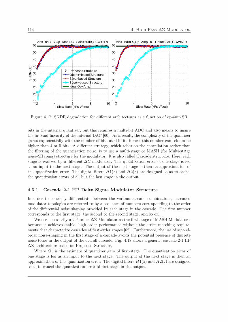
114 4. High-Pass ∆Σ Modulator
2 4 6 8 1015
20
25
30
35
40
45
50
55
Slew Rate (xFs V/sec)
SN
DR
(dB
)
Vin=−8dBFS,Op−Amp DC−Gain=60dB,GBW=5Fs
2 4 6 8 1015
20
25
30
35
40
45
50
55
Slew Rate (xFs V/sec)
Proposed StructureOberst−based StructureSilva−based StructureBoser−based StructureIdeal Op−Amp
Vin=−8dBFS,Op−Amp DC−Gain=60dB,GBW=7Fs
Figure 4.17: SNDR degradation for different architectures as a function of op-amp SR
bits in the internal quantizer, but this requires a multi-bit ADC and also means to insurethe in-band linearity of the internal DAC [60]. As a result, the complexity of the quantizergrows exponentially with the number of bits used in it. Hence, this number can seldom behigher than 4 or 5 bits. A different strategy, which relies on the cancellation rather thanthe filtering of the quantization noise, is to use a multi-stage or MASH (for Multi-stAgenoise-SHaping) structure for the modulator. It is also called Cascade structure. Here, eachstage is realized by a different ∆Σ modulator. The quantization error of one stage is fedas an input to the next stage. The output of the next stage is then an approximation ofthis quantization error. The digital filters H1(z) and H2(z) are designed so as to cancelthe quantization errors of all but the last stage in the output.
4.5.1 Cascade 2-1 HP Delta Sigma Modulator Structure
In order to concisely differentiate between the various cascade combinations, cascadedmodulator topologies are referred to by a sequence of numbers corresponding to the orderof the differential noise shaping provided by each stage in the cascade. The first numbercorresponds to the first stage, the second to the second stage, and so on.
We use necessarily a 2nd order ∆Σ Modulator as the first-stage of MASH Modulators,because it achieves stable, high-order performance without the strict matching require-ments that characterize cascades of first-order stages [62]. Furthermore, the use of second-order noise-shaping in the first stage of a cascade avoids the potential presence of discretenoise tones in the output of the overall cascade. Fig. 4.18 shows a generic, cascade 2-1 HP∆Σ architecture based on Proposed Structure,
Where G1 is the estimate of quantizer gain of first-stage. The quantization error ofone stage is fed as an input to the next stage. The output of the next stage is then anapproximation of this quantization error. The digital filters H1(z) and H2(z) are designedso as to cancel the quantization error of first stage in the output.

115
−
AnalogInput
high passfilter
−
filterhigh pass
DAC
DAC
−
−
Cancellation Logic
OutputDigital
0.5
1/5
z−1
1+z−1z−1
1+z−1 H1(z)
0.5 0.5 4/5
G1
H2(z)z−1
1+z−1
Figure 4.18: Generic architecture of cascade HP ∆Σ modulator based on Proposed Struc-ture
4.5.2 Quantizer Linear Model and Quantizer Gain Calculation
The linear model of the quantizer, shown in Fig. 3.5 on Page 69 is very important inour design of cascaded ∆Σ modulator structure. This model approximates the non-linearquantizer by a gain G called ‘quantizer gain’ in series with an additive gaussian noise source.This approximation which is valid when the quantization step is small as compared to thesignal amplitude, is also used for low-resolution quantizers where it is not verified.
The gain of the linear model for multi-bit quantizer is naturally determined by the ratioof the step size to the distance between adjacent thresholds. However, the gain of a binaryquantizer is not defined so easily because a binary quantizer has only one threshold [60].If the statistical properties of quantizer input are known, an obvious optimality criterionfor gain G is to minimize the average power of the error sequence e. This is defined as theexpected (or mean) value of e2.
σ2e =
1
N
N∑
n=0
e(n)2
Since e = v − Gy, where v is quantizer output, y is quantizer input and G is quantizergain, the average power of e can be written as,
σ2e =
1
N
N∑
n=0
(v(n) − G · y(n))2
This is minimized for,
G =
1
N
∑Nn=0 v(n)y(n)
1
N
∑Nn=0 y(n)2
(4.34)
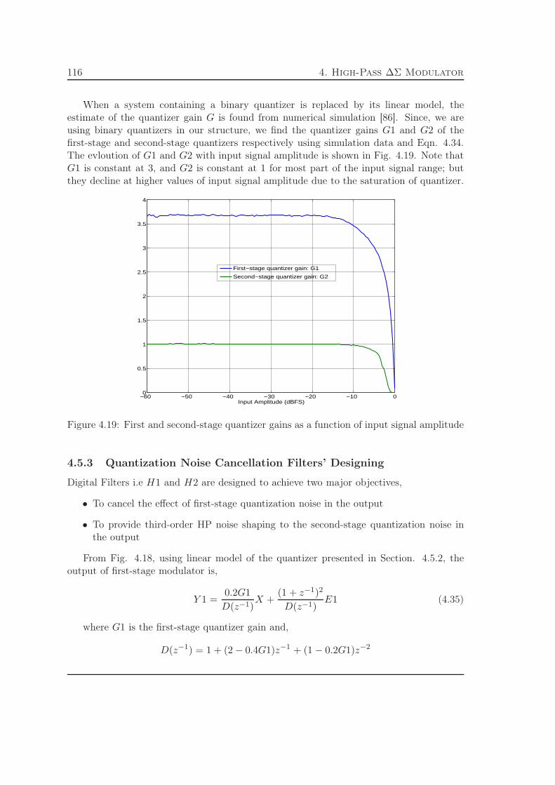
116 4. High-Pass ∆Σ Modulator
When a system containing a binary quantizer is replaced by its linear model, theestimate of the quantizer gain G is found from numerical simulation [86]. Since, we areusing binary quantizers in our structure, we find the quantizer gains G1 and G2 of thefirst-stage and second-stage quantizers respectively using simulation data and Eqn. 4.34.The evloution of G1 and G2 with input signal amplitude is shown in Fig. 4.19. Note thatG1 is constant at 3, and G2 is constant at 1 for most part of the input signal range; butthey decline at higher values of input signal amplitude due to the saturation of quantizer.
−60 −50 −40 −30 −20 −10 00
0.5
1
1.5
2
2.5
3
3.5
4
Input Amplitude (dBFS)
First−stage quantizer gain: G1
Second−stage quantizer gain: G2
Figure 4.19: First and second-stage quantizer gains as a function of input signal amplitude
4.5.3 Quantization Noise Cancellation Filters’ Designing
Digital Filters i.e H1 and H2 are designed to achieve two major objectives,
• To cancel the effect of first-stage quantization noise in the output
• To provide third-order HP noise shaping to the second-stage quantization noise inthe output
From Fig. 4.18, using linear model of the quantizer presented in Section. 4.5.2, theoutput of first-stage modulator is,
Y 1 =0.2G1
D(z−1)X +
(1 + z−1)2
D(z−1)E1 (4.35)
where G1 is the first-stage quantizer gain and,
D(z−1) = 1 + (2 − 0.4G1)z−1 + (1 − 0.2G1)z−2

117
and similarly the output of second-stage modulator is,
Y 2 =G2z−1
1 + (1 − G2)z−1E1 +
1 + z−1
1 + (1 − G2)z−1E2 (4.36)
where E1 is the quantization noise of first-stage and is the input of the second-stage,and G2 is the quantizer gain of second-stage.
4.5.3.1 Second-Stage Quantizer Gain G2
Simulation result presented in Fig. 4.19 suggests that G2 is almost equal to 1 for mostpart of the signal range. Putting this value in Eq. 4.36, we get a nice expression for Y 2,
Y 2 = z−1E1 + (1 + z−1)E2 (4.37)
4.5.3.2 First-Stage Quantizer Gain G1
Assumption of a value for G1 plays a major role in determination of digital filters. Wedefine three models based on assumption of three different values for G1:
• In the hypothetical model, we assume G1 to be equal to 5, which is not in accordancewith simulation data presented in Fig. 4.19. Nevertheless, this assumption results ina nice expression for Y 1,
Y 1 = X + (1 + z−1)2E1
Now solving the equation,
Y 1 · H1 + Y 2 · H2 = −z−1X + (1 + z−1)3E2 (4.38)
leads to very simple digital filters,
H1 = −z−1
and,H2 = (1 + z−1)2
• In this model, which we call ‘Proposal 1’, we assume G1 to be equal to 3.7, whichis true as shown in Fig. 4.19 for most part of the input signal range. Putting thisassumed value of G1 in Eqn. 4.35 leads us to,
Y 1 =0.74
1 + 0.52z−1 + 0.26z−2X +
(1 + z−1)2
1 + 0.52z−1 + 0.26z−2E1 (4.39)
Now solving the set of Eqns. 4.37, 4.38 and 4.39 leads to the digital filters,
H1 = −z−1 − 0.52z−2 − 0.26z−3
and,H2 = (1 + z−1)2

118 4. High-Pass ∆Σ Modulator
• As shown in Fig. 4.19, the value of G1 varies between 3 and 0.5. We have testedthe system performance at multiple values of G1 in this range. As we decrease thevalue of G1, the dynamic range increases but the SNR decreases. We find that takingG1 to be equal to 3 gives the best compromise between dynamic range and SNR.Therefore, the third model, which we call ’Proposal 2’, consists of assuming G1 tobe equal to 3. Working on the same pattern as the previous model, we find thefirst-stage output as,
Y 1 =0.6z−2
1 + 0.8z−1 + 0.4z−2X +
(1 + z−1)2
1 + 0.8z−1 + 0.4z−2E1 (4.40)
Solution of the set of Eqns. 4.37, 4.38 and 4.40 now gives us the digital filters to be,
H1 = −z−1 − 0.8z−2 − 0.4z−3
and,
H2 = (1 + z−1)2
So, three different assumptions for G1 result in three different values for H1. H2remains constant. When we fill these three sets of values in Fig. 4.18, we get three models.
We have simulated these three set of values for an over-sampling ratio (OSR) of 32.Simulation results are presented in Fig. 4.20. In this plot, we have added the SNR curveof the theoretical third-order ∆Σ modulator for reference.
−60 −50 −40 −30 −20 −10 020
30
40
50
60
70
80
90
Input Amplitude (dBFS)
SQ
NR
(dB
)
Proposal2:G1=3.0
Proposal1:G1=3.7
Traditional:G1=5.0
Theoretical curve
Figure 4.20: Plot of SNR Vs Input Signal for three cascaded HP ∆Σ structures based onProposed structure

119
Results presented in Fig. 4.20 show that the three models perform almost equallygood in low-signal range. It is in the high-signal range that our proposals give a superiorperformance than the classical architecture. This improved performance is due to moreaccurate and systematic approximation for quantizer gain G1.
−15 −10 −5 030
40
50
60
70
80
90
Input Amplitude (dBFS)
SQ
NR
(dB
)
Proposal2:G1=3.0
Proposal1:G1=3.7
Traditional:G1=5.0
Theoretical curve
(b)4.5dBFS
(a)3dBFS
Figure 4.21: SNR vs. High Input Signal for three cascaded HP ∆Σ models, (a) Increase indynamic range achieved by Proposal 1 over Classic Architecture (b) Increase in dynamicrange achieved by Proposal 2 over Classic Architecture
Figure. 4.21 shows the SNR curves of three models for only the higher values of inputsignal to highlight the improvement achieved by two proposals over Classic Architecture.It shows that Proposal 1 and Proposal 2 give 3 dB and 4.5 dB increase, respectively, indynamic range over Classic Architecture. Thus, Proposal 2 gives the best performancewith the highest dynamic range.
Input -20 -15 -10 -5 -4 -2Classical 65 69.8 73.2 65.9 62.5 57.8
Proposal 1 63.8 69.1 74.0 74.7 71.6 62.1Proposal 2 62.2 67.0 72.2 76.5 76.6 68.2
Table 4.1: SNRs(dB) for three models at different values of input(dB)
Table. 4.1 gives SNRs for three modulators at different values of input signal amplitudeto pinpoint the improvement achieved at higher values of input signal. Note that upto -10dB input signal, the three models give almost equal performance with the maximumdifference of only 3dB; but at -4dB input signal, Proposal 2 gives an SNR which is almost

120 4. High-Pass ∆Σ Modulator
15dB and 5dB more than the SNRs given by classic architecure and Proposal 1 respectively.Proposal 1 gives better results than Classic Model with an improvement of 3dB in highestachieved SNR and an improvement of 3dB in dynamic range; Proposal 2 provides evenbetter results with an improvement of 4dB in maximum attained SNR and an improvementof 4.5dB in dynamic range.
The problem associated with MASH structures is that there is a high level of matchingneeded between analog coefficients and digital filters. In case of any mismatch, the SNDRperformance is degraded. From fabrication point of view, digital filters are quite percisewhile there is a degree of inaccuracy involved in analog coefficients implementation. To givean idea of performance degradation, we perform monte-carlo simulation of the proposedcascade structure (i-e Proposal 2) by varying the analog coefficients and fixing the digitalfilters. The 8192 points montecarlo simulation has been carried out by varying all thecoefficients with an standard deviation of .1%. The input signal is set at -8dBFS. Thehistogram of the resulting output is shown in Fig. 4.22, it has a mean of 72.9dB and anstandard deviation of 0.31dB.
71.5 72 72.5 73 73.5 740
100
200
300
400
500
600
SQNR (dB)
Num
ber
of o
ccur
renc
e
Mean=72.9dBSt. Deviation=0.31dB
Figure 4.22: Proposed cascaded architecture’s sensibility to analog and digital components’mismatches
Analog coefficients’ inaccuracy is a direct consequence of the capacitor ratio mismatchin the circuit. Other analog imperfections that change the NTF and STF of individualMASH stages and consequently result in leakage of the quantization noise due to themismatch of digital filters with analog circuits are finite dc-gain, finite GBW productand finite SR of the amplifiers. Adaptive digital correction of these analog errors is awidely ivestigated area. This adaptive calibration can be carried out off-line [18], on-line[19, 20, 21, 22, 23] or by test-signal injection [24]. All of these techniques come at the priceof increased circuit complexity and power consumption.
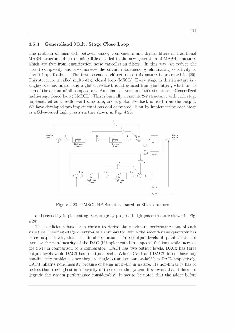
121
4.5.4 Generalized Multi Stage Close Loop
The problem of mismatch between analog components and digital filters in traditionalMASH structures due to nonidealities has led to the new generation of MASH structureswhich are free from quantization noise cancellation filters. In this way, we reduce thecircuit complexity and also increase the circuit robustness by eliminating sensitivity tocircuit imperfections. The first cascade architecture of this nature is presented in [25].This structure is called multi-stage closed loop (MSCL). Every stage in this structure is asingle-order modulator and a global feedback is introduced from the output, which is thesum of the output of all comparators. An enhanced version of this structure is Generalizedmulti-stage closed loop (GMSCL). This is basically a cascade 2-2 structure, with each stageimplemented as a feedforward structure, and a global feedback is used from the output.We have developed two implementations and compared. First by implementing each stageas a Silva-based high pass structure shown in Fig. 4.23:
−high pass
filter filterhigh pass
−
DigitalOutput
DAC1
DAC2
DAC3
AnalogInput
high passfilter
high passfilter
−
−
−
z−1
1+z−1
3
z−1
1+z−1
z−1
1+z−1z−1
1+z−1
0.4 0.6
1
2
2
0.20.2
0.20.20.25
Figure 4.23: GMSCL HP Structure based on Silva-structure
and second by implementing each stage by proposed high pass structure shown in Fig.4.24:
The coefficients have been chosen to derive the maximum performance out of eachstructure. The first-stage quantizer is a comparator, while the second-stage quantizer hasthree output levels, thus 1.5 bits of resolution. Three output levels of quantizer do notincrease the non-linearity of the DAC (if implemented in a special fashion) while increasethe SNR in comparison to a comparator. DAC1 has two output levels, DAC2 has threeoutput levels while DAC3 has 5 output levels. While DAC1 and DAC2 do not have anynon-linearity problems since they are single bit and one-and-a-half bits DACs respectively,DAC3 inherits non-linearity because of being multi-bit in nature. Its non-linearity has tobe less than the highest non-linearity of the rest of the system, if we want that it does notdegrade the system performance considerably. It has to be noted that the adder before
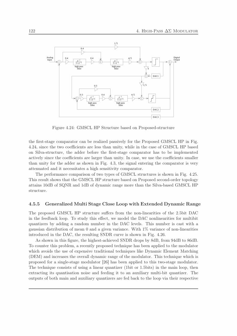
122 4. High-Pass ∆Σ Modulator
−high pass
filter
−
filterhigh pass
−
DigitalOutput
DAC1
DAC2
DAC3
AnalogInput
high passfilter
high passfilter
−
−
4/5z−1
1+z−1z−1
1+z−1
1/5
z−1
1+z−1z−1
1+z−1
3
1/5
4/50.4 0.4
0.4
0.3 0.4
0.3
Figure 4.24: GMSCL HP Structure based on Proposed-structure
the first-stage comparator can be realized passively for the Proposed GMSCL HP in Fig.4.24, since the two coefficients are less than unity, while in the case of GMSCL HP basedon Silva-structure, the adder before the first-stage comparator has to be implementedactively since the coefficients are larger than unity. In case, we use the coefficients smallerthan unity for the adder as shown in Fig. 4.3, the signal entering the comparator is veryattenuated and it necessitates a high sensitivity comparator.
The performance comparison of two types of GMSCL structures is shown in Fig. 4.25.This result shows that the GMSCL HP structure based on Proposed second-order topologyattains 10dB of SQNR and 1dB of dynamic range more than the Silva-based GMSCL HPstructure.
4.5.5 Generalized Multi Stage Close Loop with Extended Dynamic Range
The proposed GMSCL HP structure suffers from the non-linearities of the 2.5bit DACin the feedback loop. To study this effect, we model the DAC nonlinearities for multibitquantizers by adding a random number in the DAC levels. This number is cast with agaussian distribution of mean 0 and a given variance. With 1% variance of non-linearitiesintroduced in the DAC, the resulting SNDR curve is shown in Fig. 4.26.
As shown in this figure, the highest-achieved SNDR drops by 8dB, from 94dB to 86dB.To counter this problem, a recently proposed technique has been applied to the modulatorwhich avoids the use of expensive traditional techniques like Dynamic Element Matching(DEM) and increases the overall dynamic range of the modulator. This technique which isproposed for a single-stage modulator [26] has been applied to this two-stage modulator.The technique consists of using a linear quantizer (1bit or 1.5bits) in the main loop, thenextracting its quantisation noise and feeding it to an auxiliary multi-bit quantizer. Theoutputs of both main and auxiliary quantizers are fed back to the loop via their respective

123
−60 −50 −40 −30 −20 −10 0−20
0
20
40
60
80
100
120
Input Signal Amplitude (dBFS)
SQ
NR
(dB
)
Silva−based GMSCL HP structure
Proposed GMSCL HP structure
Theoretical fourth order curve
10dB
1dB
Figure 4.25: Performance comparison of two GMSCL HP structures
DACs. The resulting modulator configuration is shown in Fig. 4.27
Since the quantization noise of main quantizer is fed to the auxiliary and more ag-gressive quantizer, the output of which is injected back into the main loop, it allows themodulator to process the signals beyond the full-scale (FS) range of the main quantizer;thus the increased DR of the system and hence the increased SNDR performance. Theother major advantage of this system comes from the fact that the auxiliary quantizer onlyprocesses the quantization noise of the main stage, thus its output is pseudorandom andit mixes up the non-linearities associated with itself. In the frequency domain, the peaksassociated with the nonlinearities are flattened out across the frequency band (0 → Fs)and thus reduced by a factor of OSR. Thus, no tones are produced by this nonlinear DACas it processes only the quantization noise. The sum of two DACs associated with thefirst-stage and second-stage comparators is a three level signal i-e Vref,0 and -Vref and isinherently linear. Thus the total signal being fed back by the DACs is linear, rendering theoverall system less sensitive to DAC nonlinearities and avoiding the costly techniques likeDEM. To show the efficacity of the proposed architecture, behavioural simulations havebeen performed in matlab. The first simulation consists of ideal DACs i-e with no non-linearities to show that the proposed architecture achieves extended DR. To compare theequivalent architectures, the second-stage quantizer of the traditional topology has been
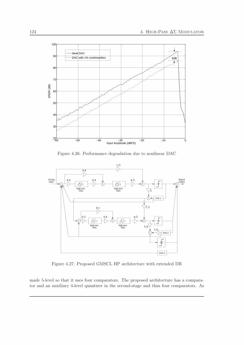
124 4. High-Pass ∆Σ Modulator
−60 −50 −40 −30 −20 −10 020
30
40
50
60
70
80
90
100
Input Amplitude (dBFS)
SN
DR
(dB
)
Ideal DAC
DAC with 1% nonlinearities 8dB
Figure 4.26: Performance degradation due to nonlinear DAC
DAC3
DAC2
−high pass
filter
−
filterhigh pass
−DAC1
AnalogInput
high passfilter
high passfilter
−
−
OutputDigital
−−−
1/5
4/5z−1
1+z−1z−1
1+z−1
1/5
z−1
1+z−1z−1
1+z−1
3
4/50.4 0.4
0.4
0.3 0.4
0.3
1/65/6
Figure 4.27: Proposed GMSCL HP architecture with extended DR
made 5-level so that it uses four comparators. The proposed architecture has a compara-tor and an auxiliary 4-level quantizer in the second-stage and thus four comparators. As

125
shown in the simulation result in Fig. 4.28, we achieve an improvement of 3.5dB in DRand 1dB in SNDR.
−60 −50 −40 −30 −20 −10 0 1010
20
30
40
50
60
70
80
90
100
110
Input Amplitude (dBFS)
SN
DR
(dB
)
Proposed
Traditional
Figure 4.28: Extended DR obtained by auxiliary quantizer and ideal DACs
The real advantage of the proposed structure becomes evident in the presence of DACnonlinearities since it is very robust against them in contrast to the traditional structure.Next, the modeling of DAC nonlinearities with mean 0 and variance 1% has been introducedin these two structures. The simulation result presented in Fig. 4.29 shows that thetraditional modulator loses 10dB of peak SNDR, while the proposed structre only loses 4dB.Thus, eventually, in the presence of DAC nonlinearities, the proposed structure providesa 7dB better performance than the traditional one from the peak SNDR standpoint and4dB performance improvement from the DR standpoint.
At -20dBFS input signal, the spectrum of the output signal of two modulators has beencaptured and exposed in Fig. 4.30.
It shows that the noise floor of the traditional topology is more elevated that the pro-posed one, because of its sensitivity to DAC nonlinearities. There are no signal distortionsin both cases because these are multi-stage systems and multi-bit quantizers only processthe quantization noise of first stage. So any DAC nonlinearities only result in noise floorelevation, which is more in the case of traditional scheme than the proposed one.
4.6 Conclusion
In this chapter, the principle of high-pass ∆Σ modulator has been presented. Ideal per-formance of a high-pass ∆Σ modulator is equivalent to that of the corresponding low-pass

126 4. High-Pass ∆Σ Modulator
−60 −50 −40 −30 −20 −10 0 1010
20
30
40
50
60
70
80
90
100
110
Input Amplitude (dBFS)
SN
DR
(dB
)Proposed
Traditional7dB
Figure 4.29: Performance comparison of two GMSCL HP structures with 1% DAC non-linearities
10−5
10−4
10−3
10−2
10−1
100
−150
−100
−50
0
Frequency (xFs Hz)
PS
D (
dB/H
z)
Proposed, SNDR=78dB
Traditional, SNDR=75dB
Figure 4.30: Output spectrum of two GMSCL topologies showing the high DAC-nonlinearity immunity of the Proposed scheme

127
modulator. But in the presence of low-frequency noise, high-pass modulator performs muchbetter since it eliminates completely the low frequency noise. Traditional architecture ofhigh-pass modulator has been presented, followed by two more state-of-the-art feedforwardtopologies. A new feedforward topology has been proposed which results in the simplifieddesign since it eliminates the need of a summing amplifier and performs better in the pres-ence of op-amp non-idealities as shown in simulation results. A new MASH structure forhigh-pass ∆Σ modulator has also been presented which increases the input dynamic rangeby and highest-achieved SNDR significantly. Finally an enhanced version of MSCL calledGMSCL has been elaborated which is free from digital cancellation filters and reduces thecircuit complexity. A new architecture of GMSCL has been presented which is based onthe proposed second-order feedforward topology. This new GMSCL high-pass modulatorachieves 10dB of SNDR over already established GMSCL structure and reduces the circuitcomplexity and power consumption.

128 4. High-Pass ∆Σ Modulator
129
Chapter 5
High-Pass Filter Implementation
5.1 Introduction
High Pass filter is a major building block of HP ∆Σ modulator. It enjoys the sameimportance in an HP modulator as an integrator enjoys in an LP modulator. The transferfunction for the HP filter is realised by applying the transformation, z → −z, to a SCintegrator:
HLP (z) =z−1
1 − z−1(5.1)
resulting in:
HHP (z) =−z−1
1 + z−1(5.2)
This filter has a zero at dc in contrast to a zero at Fs/2 for the SC integrator. Thistransfer function can be described such that, each output sample is the negative of thesum of the previous input and the previous output. HP filter design has been a majorbottle neck in the development of HP modulators. In the absence of an efficient HP filterlittle progress could be made in HP modulators. But recently, some interesting designshave been proposed. This chapter presents three state of the art of HP filters namelyintegrator-based filter, chopper-based filter and improved filter. The integrator-based filteris realized by introducing a feedback loop around the integrator by using a capacitor whichis twice the size of the integrating capacitor. The chopper-based filter on the other isbased on chopping the input signal and output signal of the integrator thus performing thesignal processing in baseband. The improved structure, combines the advantages of bothfilters and rejects their shortcomings. The brief review of each filter is followed by detailedtheoretical analysis. In the end the theoretical claims are proved by SPECTRE-simulationresults.

130 5. High-Pass Filter Implementation
5.2 Integrator-based Structure
The first HP filter implementation shown in Fig. 5.1 was presented in [27] for band-pass∆Σ modulator implementation.
−
+
+
−
input+
input−
Td
Td
Sd
Sd
T
T
S
ST
T
Sd
Sd
S
S
Td
Td
C1A
C1B
C3A
C2A
C2B
C3B
out put−
out put+
Figure 5.1: HP filter made by a feedback loop around integrator
It is designed by introducing an extra feed-back loop around the integrator, such thatthe transfer function for the HP filter is realised. This implementation suffers from variousdrawbacks which are listed as:
1. It has increased sensitivity to noise in the amplifier [28], as the extra feed-back loopresults in the amplifier noise being sampled by both the integrating capacitor andthe extra feed-back capacitor
2. The switches thermal noise level contribution to the output is augmented
3. The extra feedback capacitors significantly increase the capacitive loading of theamplifier, increasing the power consumption [27]
However, this implementation offers many advantages when compared to a band-passsolution, allowing the specifications for the amplifier design to be relaxed significantly [87].
5.2.1 Switch Noise
Two noise sources intrinsic to the MOS switches, thermal noise and flicker or 1/f noise,can potentially corrupt the filter output. Thermal noise is caused by the random motionof charge carriers in the channel of the device. This results in random fluctuation of thedrain current. 1/f noise is generated by trapping and release of charge carriers during their

131
movement in the channel. It is associated with flow of direct current in the device. Inthe analysis of switch noise below, 1/f noise is considered negligible because the currentflow in these switches consists of short pulses occuring at the clock rate and hence there isno continuous flow of charge. The thermal noise contributed by the MOS switches in thisHP filter can be estimated by modeling each switch path with the sample-and-hold circuitshown in Fig. 5.2.
(a) (b)
e2Ron
S
voutvinvoutvin
Cs Cs
Ron
Figure 5.2: (a)MOS sample-and-hold circuit, (b)its equivalent noisy circuit when S is high
When S is high and the MOS switch is on, the channel is modeled as a noiseless resistor,Ron, in series with a noise source, eRon , that has a power spectral density:
SR(f) = 4kTRon
[
V 2
Hz
]
, 0 < f < ∞ (5.3)
where k is Boltzmann’s constant and T is absolute temperature. The mean squarevalue of the noise sampled onto capacitor CS is determined by integrating the noise powerspectral density, SR(f), shaped by |H(f)|2, where H(f) is the transfer function of thelow-pass filter made by Ron and CS:
e2out =
∫
∞
0
4kTRON
1 + (2πfRONCS)2df =
kT
CS
[
V 2]
, 0 < f < ∞ (5.4)
Since the sampling frequency, Fs, is much lower than the circuit bandwidth set byRon and CS, it can be shown that the process of sampling the switch noise results in thedistribution of the total noise power kT/CS into the sampling bandwidth, −Fs/2 to Fs/2in a uniform fashion due to aliasing [82]. In this HP filter, it can be seen in Fig. 5.1that during the sampling phase, switch noise is sampled onto capacitors C1A, C1B , C3A,and C3B . During the charge-transfer phase, additional noise is sampled when the chargefrom capacitors C1A, C1B , C3A, and C3B is transferred to the integration capacitors, C2A
and C2B . Since the noise sources are uncorrelated, their powers add. Therefore, the totalpower of the switch noise referred to the filter input is:
e2switch = kT
(
2
C1A+
2
C1B+
2
C3A+
2
C3B
)
(5.5)
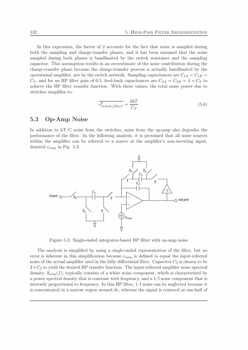
132 5. High-Pass Filter Implementation
In this expression, the factor of 2 accounts for the fact that noise is sampled duringboth the sampling and charge-transfer phases, and it has been assumed that the noisesampled during both phases is bandlimited by the switch resistance and the samplingcapacitor. This assumption results in an overestimate of the noise contribution during thecharge-transfer phase because the charge-transfer process is actually bandlimited by theoperational amplifier, not by the switch network. Sampling capacitances are C1A = C1B =CS , and for an HP filter gain of 0.5, feed-back capacitances are C3A = C3B = 4 × CS toachieve the HP filter transfer function. With these values, the total noise power due toswitches simplifies to:
e2switch,filter1 =
5kT
CS(5.6)
5.3 Op-Amp Noise
In addition to kT/C noise from the switches, noise from the op-amp also degrades theperformance of the filter. In the following analysis, it is presumed that all noise sourceswithin the amplifier can be referred to a source at the amplifier’s non-inverting input,denoted eamp in Fig. 5.3.
+
−
−1
C3
C1
Sd T
T SC2
eamp
out putinput
Sd Td
Td S
Figure 5.3: Single-ended integrator-based HP filter with op-amp noise
The analysis is simplified by using a single-ended representation of the filter, but noerror is inherent in this simplification because eamp is defined to equal the input-referrednoise of the actual amplifier used in the fully-differential filter. Capacitor C3 is chosen to be2×C2 to yield the desired HP transfer function. The input-referred amplifier noise spectraldensity, Samp(f), typically consists of a white noise component, which is characterized bya power spectral density that is constant with frequency, and a 1/f noise component that isinversely proportional to frequency. In this HP filter, 1/f noise can be neglected because itis concentrated in a narrow region around dc, whereas the signal is centered at one-half of
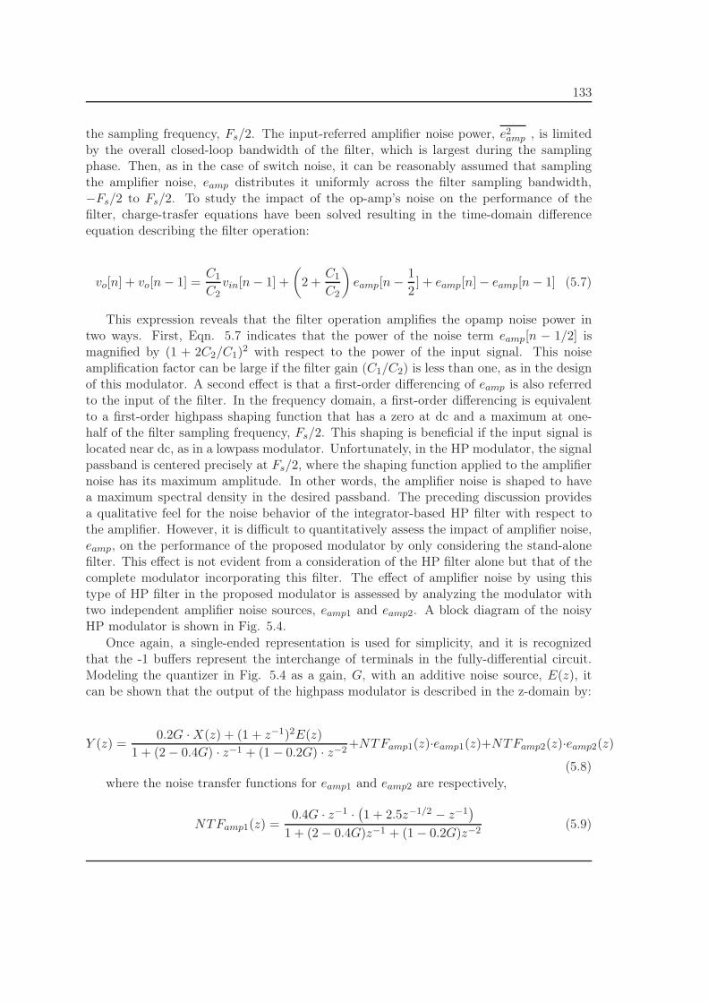
133
the sampling frequency, Fs/2. The input-referred amplifier noise power, e2amp , is limited
by the overall closed-loop bandwidth of the filter, which is largest during the samplingphase. Then, as in the case of switch noise, it can be reasonably assumed that samplingthe amplifier noise, eamp distributes it uniformly across the filter sampling bandwidth,−Fs/2 to Fs/2. To study the impact of the op-amp’s noise on the performance of thefilter, charge-trasfer equations have been solved resulting in the time-domain differenceequation describing the filter operation:
vo[n] + vo[n − 1] =C1
C2vin[n − 1] +
(
2 +C1
C2
)
eamp[n − 1
2] + eamp[n] − eamp[n − 1] (5.7)
This expression reveals that the filter operation amplifies the opamp noise power intwo ways. First, Eqn. 5.7 indicates that the power of the noise term eamp[n − 1/2] ismagnified by (1 + 2C2/C1)
2 with respect to the power of the input signal. This noiseamplification factor can be large if the filter gain (C1/C2) is less than one, as in the designof this modulator. A second effect is that a first-order differencing of eamp is also referredto the input of the filter. In the frequency domain, a first-order differencing is equivalentto a first-order highpass shaping function that has a zero at dc and a maximum at one-half of the filter sampling frequency, Fs/2. This shaping is beneficial if the input signal islocated near dc, as in a lowpass modulator. Unfortunately, in the HP modulator, the signalpassband is centered precisely at Fs/2, where the shaping function applied to the amplifiernoise has its maximum amplitude. In other words, the amplifier noise is shaped to havea maximum spectral density in the desired passband. The preceding discussion providesa qualitative feel for the noise behavior of the integrator-based HP filter with respect tothe amplifier. However, it is difficult to quantitatively assess the impact of amplifier noise,eamp, on the performance of the proposed modulator by only considering the stand-alonefilter. This effect is not evident from a consideration of the HP filter alone but that of thecomplete modulator incorporating this filter. The effect of amplifier noise by using thistype of HP filter in the proposed modulator is assessed by analyzing the modulator withtwo independent amplifier noise sources, eamp1 and eamp2. A block diagram of the noisyHP modulator is shown in Fig. 5.4.
Once again, a single-ended representation is used for simplicity, and it is recognizedthat the -1 buffers represent the interchange of terminals in the fully-differential circuit.Modeling the quantizer in Fig. 5.4 as a gain, G, with an additive noise source, E(z), itcan be shown that the output of the highpass modulator is described in the z-domain by:
Y (z) =0.2G · X(z) + (1 + z−1)2E(z)
1 + (2 − 0.4G) · z−1 + (1 − 0.2G) · z−2+NTFamp1(z)·eamp1(z)+NTFamp2(z)·eamp2(z)
(5.8)where the noise transfer functions for eamp1 and eamp2 are respectively,
NTFamp1(z) =0.4G · z−1 ·
(
1 + 2.5z−1/2 − z−1)
1 + (2 − 0.4G)z−1 + (1 − 0.2G)z−2(5.9)
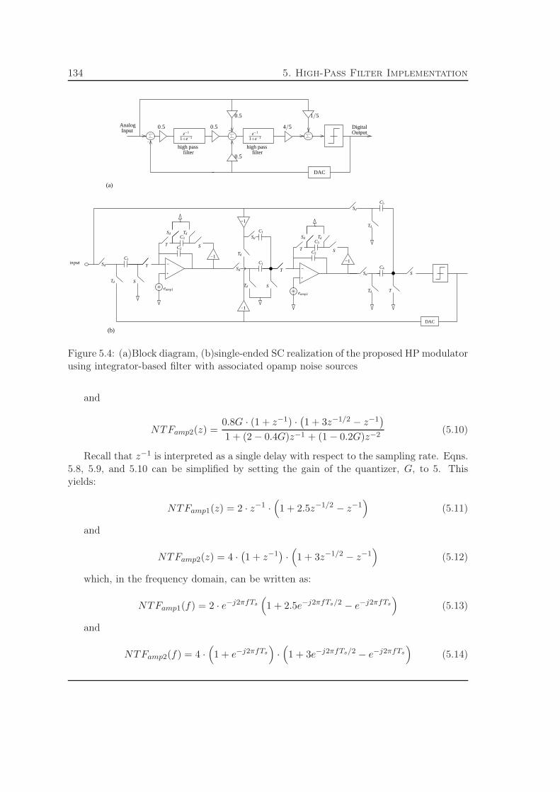
134 5. High-Pass Filter Implementation
DAC
−1
−1
−
+
−
+
−
−1
−1
(a)
(b)
−
OutputDigital
high passfilter filter
high pass
AnalogInput
DAC
S
S
T
Td S
C1
T
SdC3
C1
T
T
Sd
S
Td
C2
input
Td
C3
T
Sd Td
C2
eamp1eamp2
Sd
Sd S
Td
Td
C1
Td
Sd
Sd
C4
C5
0.5 0.5 4/5z−1
1+z−1z−1
1+z−1
0.5
0.5
1/5
Figure 5.4: (a)Block diagram, (b)single-ended SC realization of the proposed HP modulatorusing integrator-based filter with associated opamp noise sources
and
NTFamp2(z) =0.8G · (1 + z−1) ·
(
1 + 3z−1/2 − z−1)
1 + (2 − 0.4G)z−1 + (1 − 0.2G)z−2(5.10)
Recall that z−1 is interpreted as a single delay with respect to the sampling rate. Eqns.5.8, 5.9, and 5.10 can be simplified by setting the gain of the quantizer, G, to 5. Thisyields:
NTFamp1(z) = 2 · z−1 ·(
1 + 2.5z−1/2 − z−1)
(5.11)
and
NTFamp2(z) = 4 ·(
1 + z−1)
·(
1 + 3z−1/2 − z−1)
(5.12)
which, in the frequency domain, can be written as:
NTFamp1(f) = 2 · e−j2πfTs
(
1 + 2.5e−j2πfTs/2 − e−j2πfTs
)
(5.13)
and
NTFamp2(f) = 4 ·(
1 + e−j2πfTs
)
·(
1 + 3e−j2πfTs/2 − e−j2πfTs
)
(5.14)

135
where Ts is the sampling period. If e2amp1 is the input-referred noise power of the
first-stage amplifier, then the spectral density of the shaped noise from eamp1 is:
Samp1,out(f) = |NTFamp1(f)|2 ×e2amp1
Fs,
−Fs
2< f <
Fs
2(5.15)
Similarly, the spectral density of the shaped noise from eamp2 is:
Samp2,out(f) = |NTFamp2(f)|2 ×e2amp2
Fs,
−Fs
2< f <
Fs
2(5.16)
given that e2amp2 is the input-referred noise power of the second-stage amplifier. Next,
it is noted that the signal passband is centered at ±Fs/2, and the passband bandwidth isassumed to be much less than Fs. Therefore, in the passband, the spectral density of theshaped noise from eamp1 and eamp2 can be approximated as:
Samp1,inband(f) ≈ Samp1,out(f)|f=Fs/2
= |NTFamp1(f)|2f=Fs/2 ×e2amp1
Fs
= 41 ×e2amp1
Fs(5.17)
and,
Samp2,inband(f) ≈ Samp2,out(f)|f=Fs/2
= |NTFamp2(f)|2f=Fs/2 ×e2amp2
Fs
= 0 ×e2amp2
Fs= 0 (5.18)
The important and disturbing implication of Eqn. 5.17 is that within the passband,noise power from the first amplifier is amplified by a factor of 41 at the output of theproposed modulator. Fortunately, Eqn. 5.18 indicates that the inband noise contributionfrom the second amplifier is negligible because the noise shaping function NTFamp2(f) hasa zero at Fs/2. From Eqns. 5.17 and 5.18, the power of the amplifier noise present in thesignal band is approximately:
e2amp,inband ≈ [Samp1,inband(f) + Samp2,inband(f)] × B
= 41 ×e2amp1
Fs× B (5.19)
where B is the width of the passband.
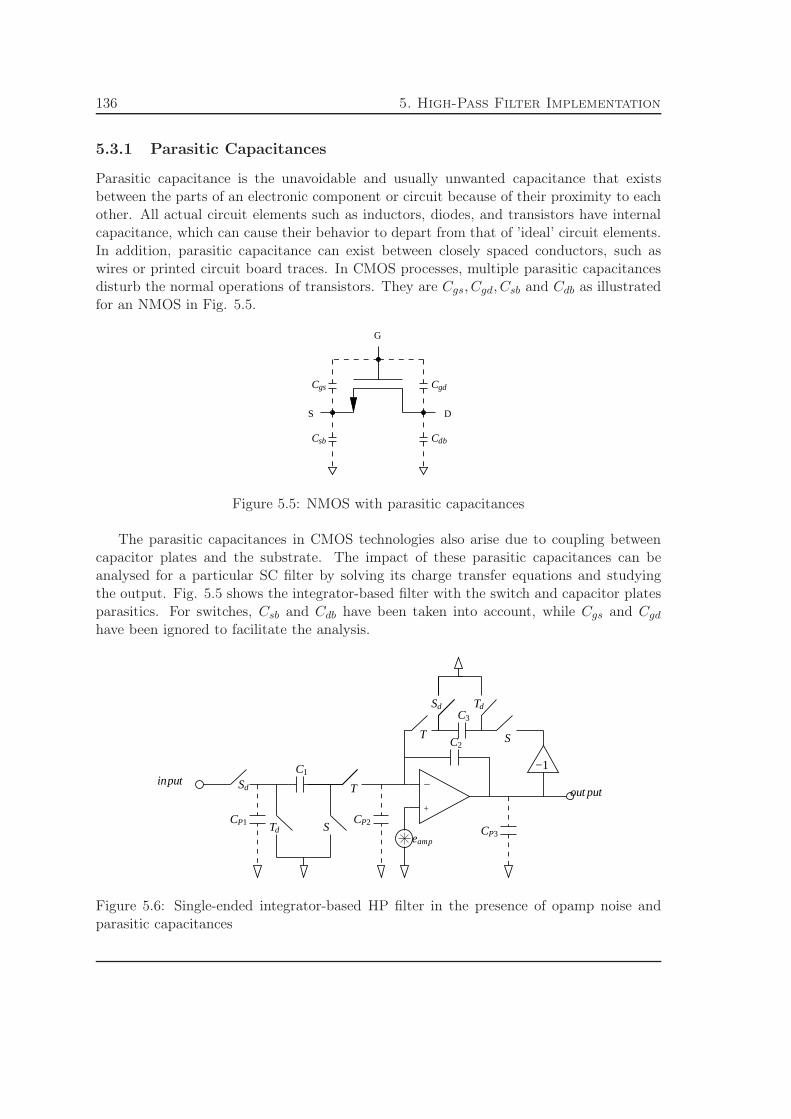
136 5. High-Pass Filter Implementation
5.3.1 Parasitic Capacitances
Parasitic capacitance is the unavoidable and usually unwanted capacitance that existsbetween the parts of an electronic component or circuit because of their proximity to eachother. All actual circuit elements such as inductors, diodes, and transistors have internalcapacitance, which can cause their behavior to depart from that of ’ideal’ circuit elements.In addition, parasitic capacitance can exist between closely spaced conductors, such aswires or printed circuit board traces. In CMOS processes, multiple parasitic capacitancesdisturb the normal operations of transistors. They are Cgs, Cgd, Csb and Cdb as illustratedfor an NMOS in Fig. 5.5.
G
S D
Csb
Cgs Cgd
Cdb
Figure 5.5: NMOS with parasitic capacitances
The parasitic capacitances in CMOS technologies also arise due to coupling betweencapacitor plates and the substrate. The impact of these parasitic capacitances can beanalysed for a particular SC filter by solving its charge transfer equations and studyingthe output. Fig. 5.5 shows the integrator-based filter with the switch and capacitor platesparasitics. For switches, Csb and Cdb have been taken into account, while Cgs and Cgd
have been ignored to facilitate the analysis.
+
−
−1
C3
T SC2
out put
C1
Sd Tinput
CP1 Td SCP2
CP3
Sd Td
eamp
Figure 5.6: Single-ended integrator-based HP filter in the presence of opamp noise andparasitic capacitances

137
To further understand the working of this ciruit, it has been broken into its constituentphases S and T in Fig. 5.7. Intuitive analysis suggests that parasitic CP3 has no influenceon the output since it just charged by the opamp and not discharged.
+
−
−1
+
−
(a)
(b)
C2
C1
CP1 CP2CP3
C3
C2
C1
CP1 CP2CP3
C3
eamp
out put
out put
input
eamp
Figure 5.7: (a) Circuit configuration in phase S, (b) phase T
The parasitic capacitance CP1 is charged to the input signal voltage in phase S. Andduring the charge-transfer phase T , this parasitic is discharged to the ground withoutaffecting the output. The effect of CP2 is tricky since the voltage across it changes in twophases with opamp noise eamp and the difference is discharged into C2. The solution ofcharge transfer equation provides the result:
vo[n]+vo[n−1] =C1
C2vin[n−1]+
(
2 +C1
C2
)
eamp[n−1
2]+
(
1 +CP2
C2
)
eamp[n]−(
1 +CP2
C2
)
eamp[n−1]
(5.20)

138 5. High-Pass Filter Implementation
This equation reflects the negative effect of parasitic capacitance CP2 on the outputof the filter. It amplifies the op-amp noise power in the passband region of the signal i-enear Fs/2. Now taking CP2 as 1% of C2, and putting this noisy and parasitic-attackedfilter in the proposed HP modulator as in the preceding section, gives the the power of theamplifier noise present in the signal band as approximately:
e2amp,inband ≈ 41.32 ×
e2amp1
Fs× B (5.21)
Comparing Eqn. 5.21 with 5.19 shows that with the inclusion of parasitic capacitance,there is a 3.3% increase in the inband noise power.
5.3.2 Op-Amp Non-Idealities
The effect of opamp non-idealities (finite dc-gain, finite GBW and slew rate) on integrator-based structue has been discussed in detail in the preceding chapter. Here, a brief summaryis presented, which serves to compare it with the other two architectures.
5.3.2.1 Finite DC-Gain
In the presence of finite opamp dc-gain, the transfer function of HP filter deviates from theideal one, as only a fraction of the last input is added to only a fraction of the last output:
Hpractical(z) = bαz−1
1 + βz−1(5.22)
where α and β are less-than-unity quantities and represent gain degradation and filterleakage (or gain and pole location perturbation) respectively.
To work out the values of α and β, the SC implementation of the integrator-basedstructure, with finite op-amp dc-gain of A0 is illustrated in Fig. 5.8:
−
+
−1
T STd
Sd T
S
Sd Td
C1
C2
CP
A0
2×C2
vout
vin
Figure 5.8: Integrator-based HP filter with finite opamp dc-gain
Where Cp represents the input parasitic capacitance of the op-amp, parasitic capaci-tance of the switches connected to the negative input of the op-amp and parasitic capac-itance associated with the plates of capacitors connected to the negative input of the

139
op-amp. Solving charge-transfer equations for this filter, keeping in view the charge-conservation law, the practical transfer function in terms of capacitances and op-ampdc-gain A0 is given by:
Hpractical(z) =Cs
Ci
A0
CsCi
+Cp
Ci+A0+3
z−1
1 +Cp
Ci+A0−1
CsCi
+Cp
Ci+A0+3
z−1
(5.23)
where Cs
Ci= b is the gain of the filter and Cp
Ci= p is the gain of the parasitic voltage.
Replacing these values in Eqn. 5.23:
Hpractical(z) = b
A0
b+p+A0+3z−1
1 + p+A0−1b+p+A0+3z−1
(5.24)
The value of b for the first HP filter in the proposed modulator is 0.5, assuming areasonable value of 0.01 for p, the exact transfer function of this filter turns out to be:
Hpractical(z) = 0.5A0
A0+3.51z−1
1 + A0−0.99A0+3.51z−1
(5.25)
Therefore the values of α and β are given by:
α =A0
A0 + 3.51, β =
A0 − 0.99
A0 + 3.51(5.26)
Using Eqn. 5.25 as the transfer function for the first HP filter of the proposed modula-tor, it is simulated at a range of values of A0 to analyse the effect of this non-ideality. Theinput signal is a sinusoid at an amplitude of 0.4 normalized with respect to quantizationstep i-e -8dBFS at frequency of 0.4993Fs. The simulation result is shown in Fig. 5.9:
This figure shows that the integrator-based filter used in proposed architecture requiresthe minimum op-amp dc gain of 45dB to acquire the ideal signal to quantization noise ratio(SQNR) for the fixed input amplitude.
5.3.2.2 Finite Gain-Bandwidth Product and Slew Rate
Finite Gain Bandwidth Product (GBW) and Slew Rate (SR) are responsible for incompleteor inaccurate charge transfer in SC circuits. With the assumption of a single-pole modelfor the op-amp, the output transient of this high-pass filter during nth integration phaseis represented by:
vout(t) = vout(nTs−Ts)+(−(1 + β)vout(nTs − Ts) + bαvin)×(1−e−tτ ), 0 < t <
Ts
2(5.27)
where vout is the output of the filter, Ts = 1/Fs is the sampling period, vin is the inputof the filter and τ = (3 + b)/2πGBW is the time constant of the op-amp comprising thefilter. In this equation, the term −2βvout(nTs−Ts) represents the discharge of the feedback

140 5. High-Pass Filter Implementation
10 15 20 25 30 35 40 45 50 55 6038
40
42
44
46
48
50
52
54
Op−Amp DC−Gain (dB)
SN
R (
dB)
Figure 5.9: SNR vs. Op-Amp DC-Gain
capacitor C3, and the term bαvin reflects the discharge of the sampling capacitor C1; bothof them discharge into the integrating capacitor C2. If this high-pass filter represents thefirst high-pass filter of a second order modulator, vin is given by:
vin = x(nTs − Ts/2) − y(nTs − Ts) (5.28)
where x is the input of the modulator and y is the output of the modulator.Slew rate of an op-amp is the maximum rate of voltage change that it can provide at
its output. Unfortunately it is practically a finite quantity that is dependant on the biascurrent of the op-amp and its load capacitance. With this nonideality of the opamp, theoutput transient of this HP filter turns out to be:
vout(t) = vout(nTs − Ts) + Vs − sgn(Vs)SRsτe−(Ts2τ
−|Vs|
SRsτ+1) (5.29)
where Vs is given by:
Vs = −(1 + β)vout(nTs − Ts) + bαvin (5.30)
Finite SR supplied by the op-amp results in changing the gain of the HP filter in anon-linear fashion and produces harmonics in the output degrading the SNDR.
Two simulations are performed by fixing the GBW of the opamp and varying the valuesof SRs and observing the output SNDR. The result is illustrated in Fig. 5.10:

141
1.5 2 2.5 3 3.5 4 4.5 525
30
35
40
45
50
55Vin=−8dBFS, OSR=32, Op−Amp DC−Gain=60dB
Slew Rate (xFs V/sec)
SN
DR
(dB
)
GBW=5FsGBW=3Fs
Figure 5.10: SNDR vs. SR for proposed modulator implemented with integrator-based HPfilter at fixed input amplitude, opamp DC-gain and GBW
The result shows that atleast a SRs of 4.2×Fs(V/sec) at a GBW of 5Fs is needed forthe proposed modulator architecture with integrator-based filter to establish the requiredperformance.
5.4 Chopper-based Structure
The second implementation as shown in Fig. 5.11, is based on the approach of modulatingthe input signal down to base band, where the signal is integrated by the SC integratorand then modulated back up to the IF frequency.
However, the signal processing still occurs at base band within the SC integrator. Thebenefits achieved by moving to an IF solution are lost once the signal is modulated backdown to base band in the analog domain, reintroducing the need for chopper stabilization(CHS) and correlated double sampling (CDS).
5.4.1 Switch Noise
In this HP filter, switch noise is sampled onto capacitors C1A and C1B during samplingphase S. During the charge-transfer phase, additional noise is sampled when the chargefrom these capacitors is transferred to the capacitors, C2A and C2B . This gives the totalpower of the switch noise referred to the filter input as:

142 5. High-Pass Filter Implementation
−
+
+
−
(a)
(b)
input+
input−
S
STd
Td
Sd
T
T
ChopB
ChopB
ChopB
ChopB
out put−
out put+
C1A
C1B
Sd
ChopA ChopAC2B
ChopA ChopAC2A
S
T
ChopA
ChopB
Figure 5.11: (a) HP filter made by chopping the input and output signal of integrator, (b)Its associated timing diagram
e2switch = kT
(
2
C1A+
2
C1B
)
(5.31)
where the factor of 2 accounts for the noise sampling in both sampling and charge-transfer phases. With the sampling capacitances of C1A = C1B = CS, the total inputreferred switch noise power is:
e2switch,filter2 =
4kT
CS(5.32)
Thus, comparing Eqns. 5.6 and 5.32, it can be shown that chopper-based structureprovides 1dB reduction in switch-noise over integrator-based structure.
5.4.2 Op-Amp Noise
To study the impact of op-amp noise on chopper-based HP filter, its single-ended versionwith op-amp noise is shown in Fig. 5.12:
In this filter, unlike the integrator-based filter, 1/f noise of the op-amp cannot beneglected because the signal is chopped to low frequencies before being processed by the op-amp. Thus the low-frequency noises of op-amp directly corrupt the useful signal. However,to keep the analysis tractable, it is assumed that sampling the amplifier noise, eamp,distributes it uniformly across the filter sampling bandwidth, −Fs/2 to Fs/2. Solving the

143
−1 −1
+
− T
C2
C1
Sd
Td S
ChopA
ChopB
ChopA
ChopB
inputout put
eamp
Figure 5.12: Single-ended chopper-based HP filter with op-amp noise
charge transfer equations of the filter, gives the time-domain equation describing the filteroperation:
vo[n] + vo[n − 1] =C1
C2vin[n − 1] +
(
C1
C2
)
eamp[n − 1
2] + eamp[n] − eamp[n − 1] (5.33)
This result illustrates that the noise term eamp[n−1/2] experiences the same amplifica-tion as the input signal, in contrast to the integrator-based structure, where it undergoesincreased amplification compared to the input signal as shown in Eqn. 5.7. On the otherhand, like the integrator-based structure, first-order differencing of the opamp noise is re-ferred to the input making the filtering of the noise in such a way that it has the highestlevel near the passband. To gain more insight into the noise performance of this filter, itis incorporated in the proposed second-order HP filter with its associated noise sources, asshown in Fig. 5.13.
−1
DAC
−1 −1 −1
−1
−1
(a)
(b)
−
OutputDigital
high passfilter filter
high pass
AnalogInput
DAC
−
+
−
+
−
Sd
T
Td S
C1
T
T
S
C1
Td
Sd
0.5 0.5 0.8z−1
1+z−1
0.5
0.5
0.2
z−1
1+z−1
C1
Sd S
Td
Td
Sd
ChopA
ChopB
ChopA
ChopB
C2
ChopA
ChopB
ChopA
ChopB
C2
eamp1eamp2
input Sd
out putC3
C4
Td
Figure 5.13: (a)Block diagram, (b)single-ended SC realization of the proposed HP modu-lator using chopper-based filter with associated opamp noise sources
Performing the necessary analysis, the output of this HP modulator in the z-domainturns out to be:
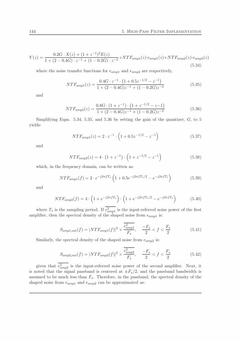
144 5. High-Pass Filter Implementation
Y (z) =0.2G · X(z) + (1 + z−1)2E(z)
1 + (2 − 0.4G) · z−1 + (1 − 0.2G) · z−2+NTFamp1(z)·eamp1(z)+NTFamp2(z)·eamp2(z)
(5.34)where the noise transfer functions for eamp1 and eamp2 are respectively,
NTFamp1(z) =0.4G · z−1 ·
(
1 + 0.5z−1/2 − z−1)
1 + (2 − 0.4G)z−1 + (1 − 0.2G)z−2(5.35)
and
NTFamp2(z) =0.8G · (1 + z−1) ·
(
1 + z−1/2 − z−1)
1 + (2 − 0.4G)z−1 + (1 − 0.2G)z−2(5.36)
Simplifying Eqns. 5.34, 5.35, and 5.36 by setting the gain of the quantizer, G, to 5yields:
NTFamp1(z) = 2 · z−1 ·(
1 + 0.5z−1/2 − z−1)
(5.37)
and
NTFamp2(z) = 4 ·(
1 + z−1)
·(
1 + z−1/2 − z−1)
(5.38)
which, in the frequency domain, can be written as:
NTFamp1(f) = 2 · e−j2πfTs
(
1 + 0.5e−j2πfTs/2 − e−j2πfTs
)
(5.39)
and
NTFamp2(f) = 4 ·(
1 + e−j2πfTs
)
·(
1 + e−j2πfTs/2 − e−j2πfTs
)
(5.40)
where Ts is the sampling period. If e2amp1 is the input-referred noise power of the first
amplifier, then the spectral density of the shaped noise from eamp1 is:
Samp1,out(f) = |NTFamp1(f)|2 ×e2amp1
Fs,
−Fs
2< f <
Fs
2(5.41)
Similarly, the spectral density of the shaped noise from eamp2 is:
Samp2,out(f) = |NTFamp2(f)|2 ×e2amp2
Fs,
−Fs
2< f <
Fs
2(5.42)
given that e2amp2 is the input-referred noise power of the second amplifier. Next, it
is noted that the signal passband is centered at ±Fs/2, and the passband bandwidth isassumed to be much less than Fs. Therefore, in the passband, the spectral density of theshaped noise from eamp1 and eamp2 can be approximated as:

145
Samp1,inband(f) ≈ Samp1,out(f)|f=Fs/2
= |NTFamp1(f)|2f=Fs/2 ×e2amp1
Fs
= 17 ×e2amp1
Fs(5.43)
and,
Samp2,inband(f) ≈ Samp2,out(f)|f=fs/2
= |NTFamp2(f)|2f=fs/2 ×e2amp2
fs
= 0 ×e2amp2
fs= 0 (5.44)
With Eqn. 5.43, it can be deduced that near the useful signal, noise power from thefirst opamp is amplified 17 times at the output of the modulator. While, fortunately, thenoise power of the second opamp is attenuated at the output because its shaping functionNTFamp2(f) has a zero at Fs/2. Using Eqns. 5.43 and 5.44, the power of the amplifiernoise present in the signal band can be approximated by:
e2amp,inband ≈ [Samp1,inband(f) + Samp2,inband(f)] × B
= 17 ×e2amp1
Fs× B (5.45)
where B is the width of the passband. The first look at Eqns. 5.45 and 5.19 suggeststhat chopper-based filter gives better performance than integrator-based filter as its opampnoise is multiplied by 17 in the output, as compared to 41 of the other. This result ismisleading because the assumption of opamp noise as being white is not valid in the caseof chopper-based filter; In this filter, the signal-processing is done at baseband, so the dc-offset and 1/f noise of the opamp corrupt the useful signal. So Eqn. 5.45 fails to capturethis corruption of the signal by the colored opamp noises and thus underestimates the totalnoise power in the signal band.
5.4.3 Parasitic Capacitances
Chopper-based filter in the presence of both opamp noise and parasitic capacitances(switch, capacitor plates and opamp) is shown in Fig. 5.14.
Performing analysis on this circuit gives the time-domain difference equation:

146 5. High-Pass Filter Implementation
−1 −1 +
−
C2
ChopA
ChopB
ChopA
ChopB
out put
eamp
C1
Sd
Td S
inputT
CP2CP1CP3
Figure 5.14: Single-ended chopper-based HP filter with parasitic capacitances
vo[n]+vo[n−1] =C1
C2vin[n−1]+
(
C1
C2
)
eamp[n−1
2]+
(
1 +CP2
C2
)
eamp[n]−(
1 +CP2
C2
)
eamp[n−1]
(5.46)This equation manifests the deterioratory effect of parasitic capacitance CP2 on the
performance of the filter. It amplifies the opamp noise near the signal band i-e aroundFs/2. Using CP2 = 0.1×C2 in this equation and putting it in the proposed HP modulator,as in the precedent section, gives the approximate power of the amplifier noise present inthe signal band as:
e2amp,inband ≈ 20 ×
e2amp1
Fs× B (5.47)
This equation shows that with the inclusion of 10% parasitic capacitance, noise powerin the signal band is increased by 17%, in contrast to 8% in the case of integrator-basedHP filter.
5.4.4 Op-Amp Non-Idealities
The consequences of opamp non-idealities on chopper-based structue are different thanthose of integrator-based structure. The fact that there is no feedback capacitor helpsreduce the requirements on opamp performances, since it is less heavily loaded. In thenext sections, finite dc-gain, GBW and slew rate of the opamp constituting chopper-basedstructure is discussed.
5.4.4.1 Finite DC-Gain
The chopper-based structure built with a finite dc-gain opamp is shown in Fig. 5.15.Where Cp represents the input parasitic capacitance of the op-amp, parasitic capaci-
tance of the switches connected to the negative input of the op-amp and parasitic capac-itance associated with the plates of capacitors connected to the negative input of theop-amp. Solving charge-transfer equations for this filter, keeping in view the charge-conservation law, the practical transfer function in terms of capacitances and op-ampdc-gain A0 is given by:

147
−1 −1 +
−
C2
ChopA
ChopB
ChopA
ChopB
C1
Sd
Td S
T
CP
A0
vinvout
Figure 5.15: Chopper-based HP filter with finite opamp dc-gain
Hpractical(z) =C1
C2
A0
C1
C2+
Cp
C2+A0+1
z−1
1 +Cp
C2+A0+1
C1
C2+
Cp
C2+A0+1
z−1
(5.48)
where C1
C2= b is the gain of the filter and Cp
C2= p is the gain of the parasitic voltage
stored on parasitic capacitance. Replacing these values in Eqn. 5.48:
Hpractical(z) = b
A0
b+p+A0+1z−1
1 + p+A0+1b+p+A0+1z−1
(5.49)
The value of b for the first HP filter in the proposed modulator architecture is 0.5,assuming a reasonable value of 0.01 i-e Cp = 1% × C2 for p, the exact transfer function ofthis filter turns out to be:
Hpractical(z) = 0.5A0
A0+1.51z−1
1 + A0+1.01A0+1.51z−1
(5.50)
Therefore the values of α and β are given by:
α =A0
A0 + 1.51, β =
A0 + 1.01
A0 + 1.51(5.51)
Using Eqn. 5.50 as the transfer function for the first HP filter of the proposed modula-tor, it is simulated at a range of values of A0 to analyse the effect of this non-ideality. Theinput signal is a sinusoid at an amplitude of 0.4 normalized with respect to quantizationstep i-e -8dBFS at frequency of 0.4993Fs. The simulation result is shown in Fig. 5.16:
This figure shows that the chopper-based structure planted in the proposed modula-tor architecture requires the minimum op-amp dc gain of 30dB (in contrast to 45dB forintegrator-based structure) to acquire the ideal signal to quantization noise ratio (SQNR)for the fixed input amplitude.
5.4.4.2 Finite Gain-Bandwidth Product and Slew Rate
The influence of finite GBW of the opamp constituting the chopper-based structure canbe represented by:
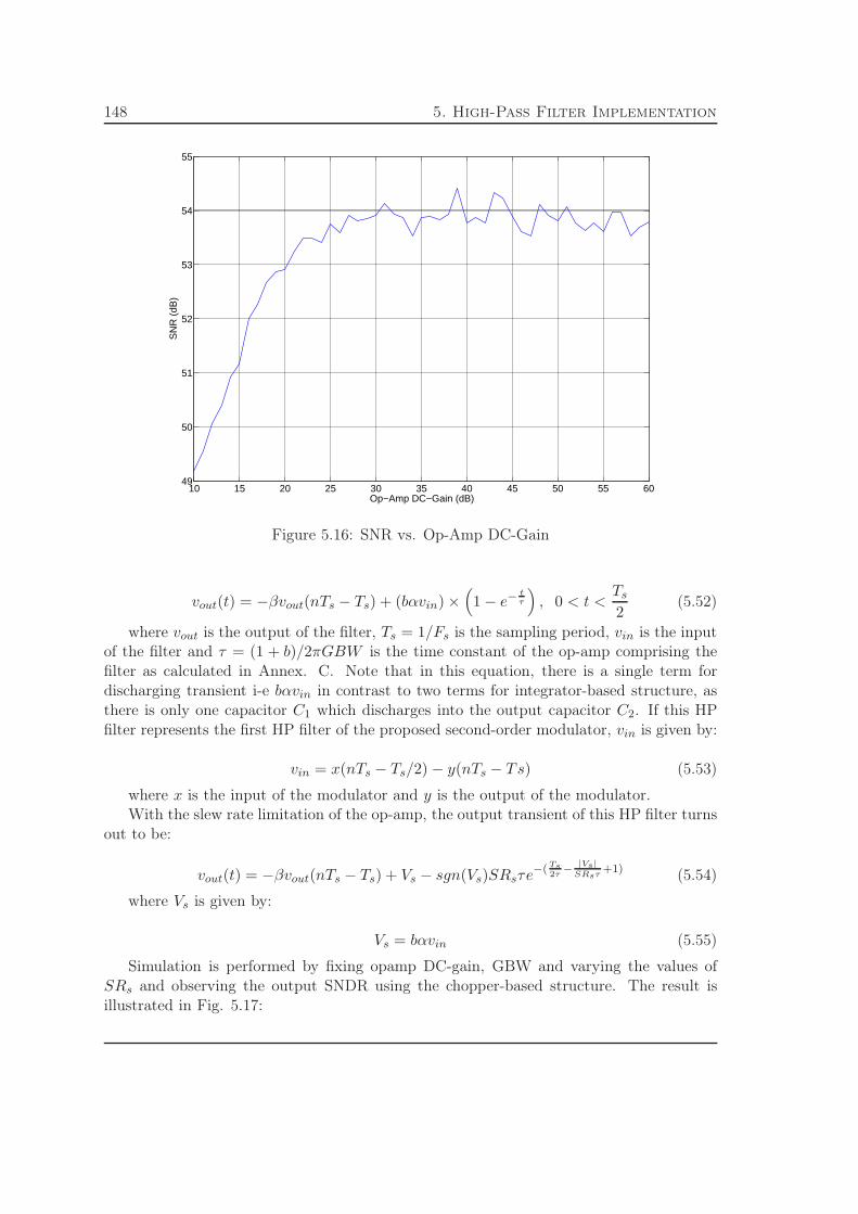
148 5. High-Pass Filter Implementation
10 15 20 25 30 35 40 45 50 55 6049
50
51
52
53
54
55
Op−Amp DC−Gain (dB)
SN
R (
dB)
Figure 5.16: SNR vs. Op-Amp DC-Gain
vout(t) = −βvout(nTs − Ts) + (bαvin) ×(
1 − e−tτ
)
, 0 < t <Ts
2(5.52)
where vout is the output of the filter, Ts = 1/Fs is the sampling period, vin is the inputof the filter and τ = (1 + b)/2πGBW is the time constant of the op-amp comprising thefilter as calculated in Annex. C. Note that in this equation, there is a single term fordischarging transient i-e bαvin in contrast to two terms for integrator-based structure, asthere is only one capacitor C1 which discharges into the output capacitor C2. If this HPfilter represents the first HP filter of the proposed second-order modulator, vin is given by:
vin = x(nTs − Ts/2) − y(nTs − Ts) (5.53)
where x is the input of the modulator and y is the output of the modulator.With the slew rate limitation of the op-amp, the output transient of this HP filter turns
out to be:
vout(t) = −βvout(nTs − Ts) + Vs − sgn(Vs)SRsτe−(Ts2τ
−|Vs|
SRsτ+1) (5.54)
where Vs is given by:
Vs = bαvin (5.55)
Simulation is performed by fixing opamp DC-gain, GBW and varying the values ofSRs and observing the output SNDR using the chopper-based structure. The result isillustrated in Fig. 5.17:

149
1 1.2 1.4 1.6 1.8 2 2.2 2.4 2.6 2.8 325
30
35
40
45
50
55
Slew Rate (xFs V/sec)
SN
DR
(dB
)
Vin=−8dBFS, OSR=32, Op−Amp DC−Gain=60dB
GBW=5FsGBW=7Fs
Figure 5.17: SNDR degradation of the proposed modulator implemented using chopper-based filter as a function of op-amp SR
The result shows that the minimum SRs of 1.8×Fs(V/sec) is needed for the proposedmodulator architecture with chopper-based filter to establish the required performance,contrary to 4.2 × Fs(V/sec) for the integrator-based one.
5.5 Improved Structure
An improved implementation of HP filter is reported in [29] and is shown in Fig. 5.18.This implementation does not suffer from the disadvantages of the previous two implemen-tations. The basic operation is such that the charge is sampled onto C1A, during S. On Tthis charge is then transferred to C2A on odd clock cycles and to C2B on even clock cycles.C1B functions in a similar manner.
This implementation is better than integrator-based filter because there is no extrafeedback loop around integrator. This has various advantageous implications: it takes sig-nificantly less area, it reduces the capacitive loading on the opamp and consequently thepower consumption, it improves the noise performance of the filter as derived analyticallyin the later sections and it improves the stability as it is no longer dependant on accuratecapacitor matching. This structure also resolves the problem of low-frequency noises asso-ciated with chopper-based structure; all the signal processing is completed at IF frequency,thus dc offset or 1/f noise no longer pollute the useful signal.
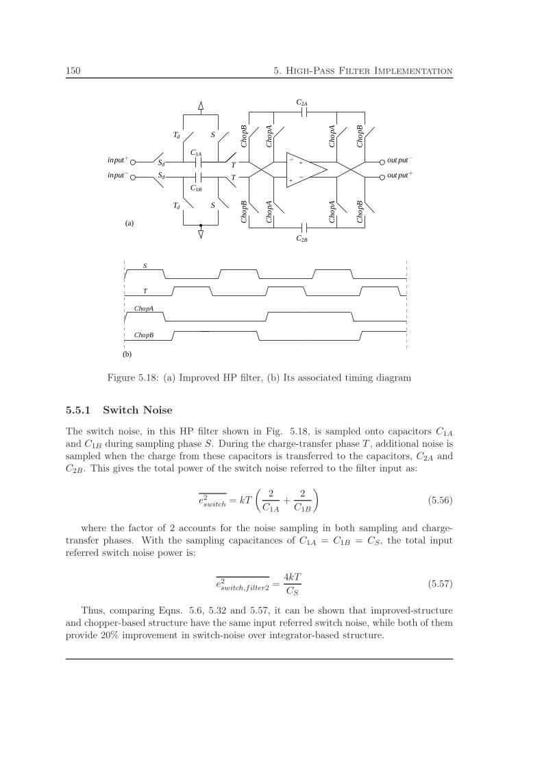
150 5. High-Pass Filter Implementation
−
+
+
−
(a)
(b)
T
ChopA
ChopB
S
Td
Td
Sd
Sd
T
T
S
S
C1A
C1B
C2A
C2B
out put−
out put+
input+
input−
Cho
pA
Cho
pAC
hopA
Cho
pB
Cho
pB
Cho
pB
Cho
pB
Cho
pA
Figure 5.18: (a) Improved HP filter, (b) Its associated timing diagram
5.5.1 Switch Noise
The switch noise, in this HP filter shown in Fig. 5.18, is sampled onto capacitors C1A
and C1B during sampling phase S. During the charge-transfer phase T , additional noise issampled when the charge from these capacitors is transferred to the capacitors, C2A andC2B . This gives the total power of the switch noise referred to the filter input as:
e2switch = kT
(
2
C1A+
2
C1B
)
(5.56)
where the factor of 2 accounts for the noise sampling in both sampling and charge-transfer phases. With the sampling capacitances of C1A = C1B = CS, the total inputreferred switch noise power is:
e2switch,filter2 =
4kT
CS(5.57)
Thus, comparing Eqns. 5.6, 5.32 and 5.57, it can be shown that improved-structureand chopper-based structure have the same input referred switch noise, while both of themprovide 20% improvement in switch-noise over integrator-based structure.

151
5.5.2 Op-Amp Noise
Like the previous two structures, the single-ended version of the improved structure is usedto study the influence of opamp noise on its performance. Its single-ended version withopamp noise is shown in Fig. 5.12:
−1
−1
+
−
Cho
pA
Cho
pB
Cho
pA
Cho
pB
T
eamp
Sd
Td S
inputout put
C1
C2
Figure 5.19: Single-ended improved HP filter with opamp noise
This figure shows that in this structure, unlike the chopper-based one, the signal isnot chopped before being processed by the opamp, therefore the op-amp sees the signalplaced near Fs/2 and hence it is not corrupted by the dc offset and 1/f noise of the opamp.For this reason, in the input-referred opamp noise eamp, 1/f can be neglected and then itcan be reasonably assumed that sampling the amplifier noise, eamp distributes it uniformlyacross the filter sampling bandwidth, −Fs/2 to Fs/2. Time-domain difference equation ofthe circuit shown in Fig. 5.19 is given by:
vo[n] + vo[n − 1] =C1
C2vin[n − 1] +
(
C1
C2
)
eamp[n − 1
2] + eamp[n] + eamp[n − 1] (5.58)
This result illustrates that the noise term eamp[n−1/2] experiences the same amplifica-tion as the input signal, in contrast to the integrator-based structure, where it undergoesincreased amplification compared to the input signal as shown in Eqn. 5.7. On the otherhand, unlike both integrator-based and chopper-based structures, no first-order differencingof the opamp noise is referred to the input; instead opamp noise is filtered by 1+z−1 func-tion, which has a lowpass characteristic, thus diminishing the noise around the passbandat Fs/2. To gain more insight into the noise performance of this filter, it is incorporatedin the proposed second-order HP filter with its associated noise sources, as shown in Fig.5.20.
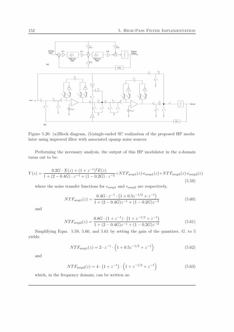
152 5. High-Pass Filter Implementation
−1
DAC
−1
−1
−1
−1
−1
(b)
−
OutputDigital
high passfilter filter
high pass
AnalogInput
DAC
−
(a)
+
− +
−
Sd
T
Td S
C1
T
Cho
pA
Cho
pB
T
Cho
pA
Cho
pB
Td
Sd
C4
Cho
pA
Cho
pB
Cho
pA
Cho
pB
T
C1
Td
Sd
0.5 0.5 0.8z−1
1+z−1
0.5
0.5
z−1
1+z−1
Sd S
Td
C3
out put
eamp2
Td S
C1
C2
eamp1
S
C1
C2
0.2
input
Td
Sd
Figure 5.20: (a)Block diagram, (b)single-ended SC realization of the proposed HP modu-lator using improved filter with associated opamp noise sources
Performing the necessary analysis, the output of this HP modulator in the z-domainturns out to be:
Y (z) =0.2G · X(z) + (1 + z−1)2E(z)
1 + (2 − 0.4G) · z−1 + (1 − 0.2G) · z−2+NTFamp1(z)·eamp1(z)+NTFamp2(z)·eamp2(z)
(5.59)where the noise transfer functions for eamp1 and eamp2 are respectively,
NTFamp1(z) =0.4G · z−1 ·
(
1 + 0.5z−1/2 + z−1)
1 + (2 − 0.4G)z−1 + (1 − 0.2G)z−2(5.60)
and
NTFamp2(z) =0.8G · (1 + z−1) ·
(
1 + z−1/2 + z−1)
1 + (2 − 0.4G)z−1 + (1 − 0.2G)z−2(5.61)
Simplifying Eqns. 5.59, 5.60, and 5.61 by setting the gain of the quantizer, G, to 5yields:
NTFamp1(z) = 2 · z−1 ·(
1 + 0.5z−1/2 + z−1)
(5.62)
and
NTFamp2(z) = 4 ·(
1 + z−1)
·(
1 + z−1/2 + z−1)
(5.63)
which, in the frequency domain, can be written as:
153
NTFamp1(f) = 2 · e−j2πfTs
(
1 + 0.5e−j2πfTs/2 + e−j2πfTs
)
(5.64)
and
NTFamp2(f) = 4 ·(
1 + e−j2πfTs
)
·(
1 + e−j2πfTs/2 + e−j2πfTs
)
(5.65)
where Ts is the sampling period. If e2amp1 is the input-referred noise power of the first
amplifier, then the spectral density of the shaped noise from eamp1 is:
Samp1,out(f) = |NTFamp1(f)|2 ×e2amp1
Fs,
−Fs
2< f <
Fs
2(5.66)
Similarly, the spectral density of the shaped noise from eamp2 is:
Samp2,out(f) = |NTFamp2(f)|2 ×e2amp2
Fs,
−Fs
2< f <
Fs
2(5.67)
given that e2amp2 is the input-referred noise power of the second amplifier. Next, it
is noted that the signal passband is centered at ±Fs/2, and the passband bandwidth isassumed to be much less than Fs. Therefore, in the passband, the spectral density of theshaped noise from eamp1 and eamp2 can be approximated as:
Samp1,inband(f) ≈ Samp1,out(f)|f=Fs/2
= |NTFamp1(f)|2f=Fs/2 ×e2amp1
Fs
= 1 ×e2amp1
Fs(5.68)
and,
Samp2,inband(f) ≈ Samp2,out(f)|f=Fs/2
= |NTFamp2(f)|2f=Fs/2 ×e2amp2
Fs
= 0 ×e2amp2
Fs= 0 (5.69)
With Eqn. 5.68, it can be deduced that near the useful signal, noise power from thefirst opamp is not amplified at the output of the modulator, in contrast to the previoustwo implementations. While, like the previous implementations, the noise power of thesecond opamp is attenuated at the output because its shaping function NTFamp2(f) hasa zero at Fs/2. Using Eqns. 5.68 and 5.69, the power of the amplifier noise present in thesignal band can be approximated by:

154 5. High-Pass Filter Implementation
e2amp,inband ≈ [Samp1,inband(f) + Samp2,inband(f)] × B
= 1 ×e2amp1
Fs× B (5.70)
where B is the width of the passband. Comparing Eqns. 5.19, 5.45 and 5.70, it becomesevident that the improved-filter has much better noise performance than the other twotopologies, when used in the proposed HP modulator.
5.5.3 Parasitic Capacitances
To assess the deterioratory effect of parasitic capacitances (due to switches, capacitor platesand opamp) on the functioning of improved HP filter, they have been included (in additionto opamp noise) in this filter as illustrated in Fig. 5.21.
−1
−1
+
−
Cho
pA
Cho
pB
Cho
pA
Cho
pB
TSd
Td S
inputout put
C1
C2
CP1 CP2CP3
Figure 5.21: Single-ended improved HP filter with parasitic capacitances
Performing analysis on this circuit gives the time-domain difference equation:
vo[n]+vo[n−1] =C1
C2vin[n−1]+
(
C1
C2
)
eamp[n−1
2]+
(
1 +CP2
C2
)
eamp[n]+
(
1 − CP2
C2
)
eamp[n−1]
(5.71)This equation manifests the deterioratory effect of parasitic capacitance CP2 on the
performance of the filter. It amplifies the opamp noise near the signal band i-e aroundFs/2. Using CP2 = 0.1×C2 in this equation and putting it in the proposed HP modulator,

155
as in the precedent section, gives the approximate power of the amplifier noise present inthe signal band as:
e2amp,inband ≈ 1.16 ×
e2amp1
Fs× B (5.72)
This equation shows that with the inclusion of 10% parasitic capacitance, noise powerin the signal band is increased by 16%. But still the inband-noise power is very smallcompared to integrator-based and chopper-based structures.
5.5.4 Op-Amp Non-Idealities
The consequences of opamp non-linearities on the improved structure are analysed in thefollowing sections and are compared with integrator-based and chopper-based structures.Like in the chopper-based structure, the absence of feedback capacitor helps reduce therequirements on opamp performances. In the next sections, finite dc-gain, GBW and slewrate of the opamp constituting the improved structure are modelled.
5.5.4.1 Finite DC-Gain
The improved structure built with a finite dc-gain opamp is shown in Fig. 5.22.
−1
−1
+
− TSd
C1
C2
Td S
Cho
pA
Cho
pB
Cho
pA
Cho
pB
vinvout
CP
A0
Figure 5.22: Improved HP filter with finite opamp dc-gain
Where Cp represents the input parasitic capacitance of the op-amp, parasitic capaci-tance of the switches connected to the negative input of the op-amp and parasitic capac-itance associated with the plates of capacitors connected to the negative input of the
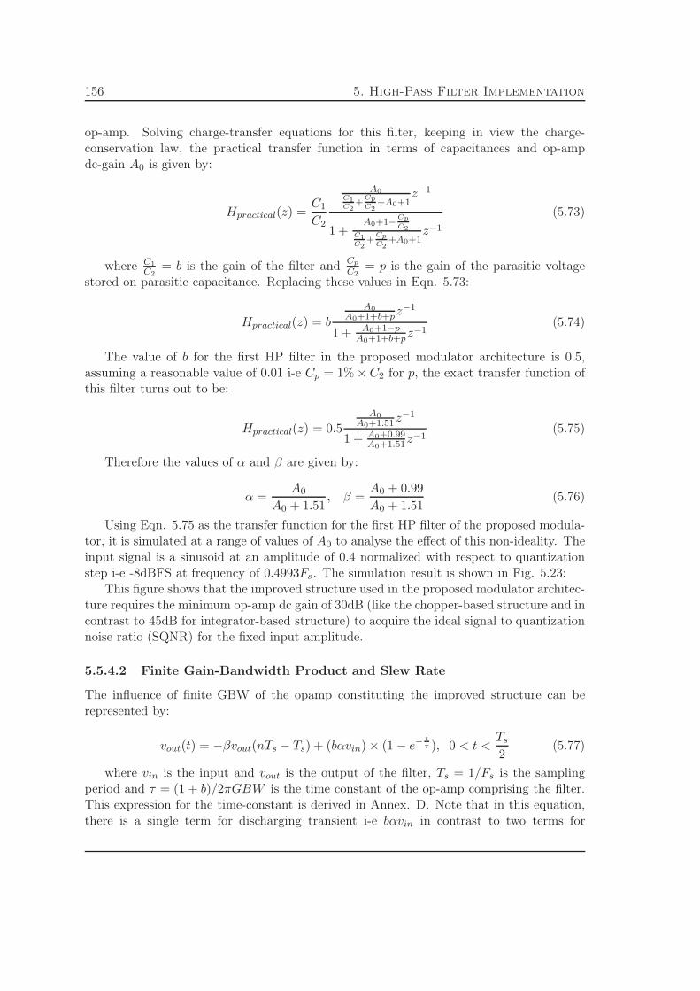
156 5. High-Pass Filter Implementation
op-amp. Solving charge-transfer equations for this filter, keeping in view the charge-conservation law, the practical transfer function in terms of capacitances and op-ampdc-gain A0 is given by:
Hpractical(z) =C1
C2
A0
C1
C2+
Cp
C2+A0+1
z−1
1 +A0+1−
Cp
C2
C1
C2+
Cp
C2+A0+1
z−1
(5.73)
where C1
C2= b is the gain of the filter and Cp
C2= p is the gain of the parasitic voltage
stored on parasitic capacitance. Replacing these values in Eqn. 5.73:
Hpractical(z) = b
A0
A0+1+b+pz−1
1 + A0+1−pA0+1+b+pz−1
(5.74)
The value of b for the first HP filter in the proposed modulator architecture is 0.5,assuming a reasonable value of 0.01 i-e Cp = 1% × C2 for p, the exact transfer function ofthis filter turns out to be:
Hpractical(z) = 0.5
A0
A0+1.51z−1
1 + A0+0.99A0+1.51z−1
(5.75)
Therefore the values of α and β are given by:
α =A0
A0 + 1.51, β =
A0 + 0.99
A0 + 1.51(5.76)
Using Eqn. 5.75 as the transfer function for the first HP filter of the proposed modula-tor, it is simulated at a range of values of A0 to analyse the effect of this non-ideality. Theinput signal is a sinusoid at an amplitude of 0.4 normalized with respect to quantizationstep i-e -8dBFS at frequency of 0.4993Fs. The simulation result is shown in Fig. 5.23:
This figure shows that the improved structure used in the proposed modulator architec-ture requires the minimum op-amp dc gain of 30dB (like the chopper-based structure and incontrast to 45dB for integrator-based structure) to acquire the ideal signal to quantizationnoise ratio (SQNR) for the fixed input amplitude.
5.5.4.2 Finite Gain-Bandwidth Product and Slew Rate
The influence of finite GBW of the opamp constituting the improved structure can berepresented by:
vout(t) = −βvout(nTs − Ts) + (bαvin) × (1 − e−tτ ), 0 < t <
Ts
2(5.77)
where vin is the input and vout is the output of the filter, Ts = 1/Fs is the samplingperiod and τ = (1 + b)/2πGBW is the time constant of the op-amp comprising the filter.This expression for the time-constant is derived in Annex. D. Note that in this equation,there is a single term for discharging transient i-e bαvin in contrast to two terms for
157
10 15 20 25 30 35 40 45 50 55 6038
40
42
44
46
48
50
52
54
Op−Amp DC−Gain (dB)
SN
R (
dB)
integrator−based filter
chopper−based filter
improved filter
ideal opamp
Figure 5.23: SNR vs. Op-Amp DC-Gain
integrator-based structure, as there is only one capacitor C1 which discharges into theoutput capacitor C2. If this HP filter represents the first HP filter of the proposed second-order modulator, vin is given by:
vin = x(nTs − Ts/2) − y(nTs − Ts) (5.78)
where x is the input of the modulator and y is the output of the modulator.With the slew rate limitation of the op-amp, the output transient of this HP filter turns
out to be:
vout(t) = −βvout(nTs − Ts) + Vs − sgn(Vs)SRsτe−(Ts2τ
−|Vs|
SRsτ+1) (5.79)
where Vs is given by:
Vs = bαvin (5.80)
To gauge the impact of finite GBW and SR on the improved filter and to compare itwith other two filter implementations, simulations are carried out by varying the valuesof SRs at two different values of GBW and observing the output SNDR. The result isillustrated in Fig. 5.24:
The result shows that the minimum SRs of 1.8×Fs(V/sec) is needed for the proposedmodulator architecture implemented with either the improved filter or the chopper-basedfilter to establish the required performance at the GBW of 5Fs. On the other hand, the

158 5. High-Pass Filter Implementation
1 2 3 4 5 625
30
35
40
45
50
55
Slew Rate (xFs V/sec)
SN
DR
(dB
)
Vin=−8dBFS, OSR=32, Op−Amp DC−Gain=60dB
1 2 3 4 5 625
30
35
40
45
50
55
Slew Rate (xFs V/sec)
GBW=5Fs GBW=7Fs
Improved FilterChopper−based FilterIntegrator−based FilterIdeal Op−Amp
Figure 5.24: SNDR vs. op-amp SR for the proposed modulator architecture
minimum SRs of 4.2×Fs(V/sec) is required at the GBW of GBW of 5Fs, if the proposedarchitecture is built with integrator-based filter.
5.5.5 High Frequency Performance Analysis
The basic purpose of this design procedure is to find an architecture of the HP filter, whichcan convert large bandwidth while consuming the least amount of power. In other words,the filter which uses an opamp with least GBW and SR and operates at maximum samplingfrequency. The simulation results in the previous sections reflect that chopper-based andimproved structure fall in this category since their GBW and SR is the least multiple ofsampling frequency Fs. In this section, this analysis is carried one step further by carryingit out in realistic simulator SPECTRE by CADENCE. For this purpose, macro-models ofthe building blocks are used.
The switches used are macro-models having Ron = 10Ω and Roff = 10MΩ. Thecapacitances used are C1 = 1pF,C2 = 2pF and C3 = 4pF . The op-amps used are single-pole macro-models having Rout = 10kΩ and Gm = 10mS thus a dc-open-loop-gain of40dB. The GBW of op-amp depends on the feedback loop or load across opamp duringthe charge transfer phase:
fT =Gm
2πCL(5.81)
The capacitive load on chopper-based and improved filter is the same and is smallerthan integrator-based filter which has an additional load because of feedback loop aroundthe integrator. This loop makes the major part of the load around the op-amp because itis twice the value of integrating capacitor. Thus the op-amp with the same dimensions willgive small GBW for integrator-based filter as compared to the other two implementations.In other words, to make the integrator-based filter work at high sampling frequencies,we have to make much aggressive op-amp compared to the other two implementations,resulting in high power consumption.
In this analysis, we measure the SNDR of the modulator by varying the samplingfrequency for each type of filter while keeping the op-amp GBW constant.

159
This result is reflected in the simulation result shown in Fig. 5.25:
1 2 3 4 5 6 7 8 9 10
x 108
0
10
20
30
40
50
60
SN
DR
(dB
)
Improved filter
Integrator−based filter
Chopper−based filter
280MHz
fs (Hz)
Figure 5.25: Performance of proposed HP modulator using three HP filters at high samplingfrequencies
This shows that chopper-based and improved filter can work at sampling frequencywhich is 280MHz higher than highest possible sampling frequency for integrator-based filterusing the same op-amp. In other words, at the same power consumption, modulator builtwith integrator-based filter can convert less bandwidth than the modulator constructedwith the other two filter topologies.
5.5.6 Noise Analysis
Another important criteria that is used to compare the filters is op-amp noise rejection. Op-amp noise consists of thermal noise which has white spectrum over the frequency of interestand Flicker Noise, which has a spectrum proportional to 1/f. In any op-amp configuration,at least four devices contribute to the noise: two input transistors and two load transistors.Since the op-amps used in the three filters are the same, we have reasonably assumed thattheir input referred noise is the same. Performance of the modulator in the presence ofop-amp noise has already been analysed theoretically for each filter. In this section, thepurpose is to validate the theoretical study by simulating the circuits in SPECTRE. Like inthe previous section, macro-models of the building blocks have been used for this purpose.
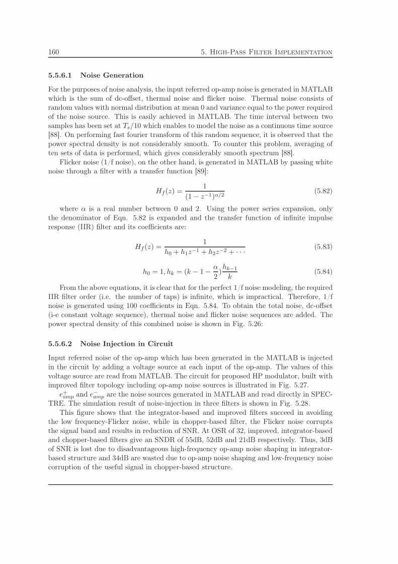
160 5. High-Pass Filter Implementation
5.5.6.1 Noise Generation
For the purposes of noise analysis, the input referred op-amp noise is generated in MATLABwhich is the sum of dc-offset, thermal noise and flicker noise. Thermal noise consists ofrandom values with normal distribution at mean 0 and variance equal to the power requiredof the noise source. This is easily achieved in MATLAB. The time interval between twosamples has been set at Ts/10 which enables to model the noise as a continuous time source[88]. On performing fast fourier transform of this random sequence, it is observed that thepower spectral density is not considerably smooth. To counter this problem, averaging often sets of data is performed, which gives considerably smooth spectrum [88].
Flicker noise (1/f noise), on the other hand, is generated in MATLAB by passing whitenoise through a filter with a transfer function [89]:
Hf (z) =1
(1 − z−1)α/2(5.82)
where α is a real number between 0 and 2. Using the power series expansion, onlythe denominator of Eqn. 5.82 is expanded and the transfer function of infinite impulseresponse (IIR) filter and its coefficients are:
Hf (z) =1
h0 + h1z−1 + h2z−2 + · · · (5.83)
h0 = 1, hk = (k − 1 − α
2)hk−1
k(5.84)
From the above equations, it is clear that for the perfect 1/f noise modeling, the requiredIIR filter order (i.e. the number of taps) is infinite, which is impractical. Therefore, 1/fnoise is generated using 100 coefficients in Eqn. 5.84. To obtain the total noise, dc-offset(i-e constant voltage sequence), thermal noise and flicker noise sequences are added. Thepower spectral density of this combined noise is shown in Fig. 5.26:
5.5.6.2 Noise Injection in Circuit
Input referred noise of the op-amp which has been generated in the MATLAB is injectedin the circuit by adding a voltage source at each input of the op-amp. The values of thisvoltage source are read from MATLAB. The circuit for proposed HP modulator, built withimproved filter topology including op-amp noise sources is illustrated in Fig. 5.27.
e+amp and e−amp are the noise sources generated in MATLAB and read directly in SPEC-
TRE. The simulation result of noise-injection in three filters is shown in Fig. 5.28.This figure shows that the integrator-based and improved filters succeed in avoiding
the low frequency-Flicker noise, while in chopper-based filter, the Flicker noise corruptsthe signal band and results in reduction of SNR. At OSR of 32, improved, integrator-basedand chopper-based filters give an SNDR of 55dB, 52dB and 21dB respectively. Thus, 3dBof SNR is lost due to disadvantageous high-frequency op-amp noise shaping in integrator-based structure and 34dB are wasted due to op-amp noise shaping and low-frequency noisecorruption of the useful signal in chopper-based structure.
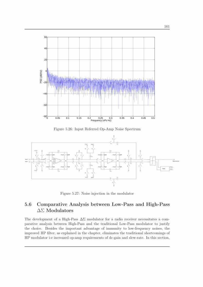
161
0 0.05 0.1 0.15 0.2 0.25 0.3 0.35 0.4 0.45 0.5−80
−60
−40
−20
0
20
40
60
Frequency (xFs Hz)
PS
D (
dB/H
z)
Figure 5.26: Input Referred Op-Amp Noise Spectrum
−
+
+
−
−
+
+
−
DAC
ChopBChopAChopA
ChopB ChopA ChopA ChopBTd
Td
Sd
Sd
S
S
T
T
ChopB
Sd
Sd
Td
Td
C5
C5
T
T
input−V re f−
ChopB
ChopB ChopBChopAChopA
ChopA ChopA ChopBTd
C4
C4
Sd
Sd
T
SS
Td
T
V re f−
V re f +
Digitalout put
input+
input−
Td
Td
Sd
Sd
S
S
V re f +
V re f−
C2A
C2B
C1A
C1B
e+amp
e−amp
C1A
C1B
Td Sd
C1A
SdTd
input+V re f +
C1B
C2A
C2B
Figure 5.27: Noise injection in the modulator
5.6 Comparative Analysis between Low-Pass and High-Pass
∆Σ Modulators
The development of a High-Pass ∆Σ modulator for a radio receiver necessitates a com-parative analysis between High-Pass and the traditional Low-Pass modulator to justifythe choice. Besides the important advantage of immunity to low-frequency noises, theimproved HP filter, as explained in the chapter, eliminates the traditional shortcomings ofHP modulator i-e increased op-amp requirements of dc-gain and slew-rate. In this section,

162 5. High-Pass Filter Implementation
10−4
10−3
10−2
10−1
−100
−90
−80
−70
−60
−50
−40
−30
−20
−10
0
integrator−based filter
Frequency (xFs Hz)
PS
D (
dB/H
z)improved filter
chopper−based filter
Figure 5.28: Modulator output spectrum in the presence of op-amp noise for three filters
a detailed comparative analysis between different architectures of HP and LP modulatorsis performed to study the trade-offs in designing a HP modulator.
5.6.1 Clipping
Op-amp clipping or saturation is a practical reality which happens due to limited voltage-swing available at the op-amp output. Feedforward structures perform better in comparisonto feedback structures in the face of this nonideality because they process lesser amountof signal. The simulation result showing both LP and HP versions of different modulatorarchitectures is presented in Fig. 5.29.
This shows that both LP and HP structures perform equally good with reference tothe parameter of op-amp saturation. The feedback structures demonstrate unstability atthe early stages of input signal level, while the feedforward structures which do not processuseful signal in the integrators/mirrored-integrators, remain stable throughout the inputsignal level even at low op-amp saturation levels.
5.6.2 Op-Amp DC-Gain
The DC-Gain of the op-amps employed in building the integrators/mirrored-integratorsis an expensive parameter which needs to be reduced as much as possible to relax therequirements on the op-amp design and to increase the speed of the op-amp at a reasonablepower consumption. Finite DC-Gain of the op-amps introduces static errors in the charge-
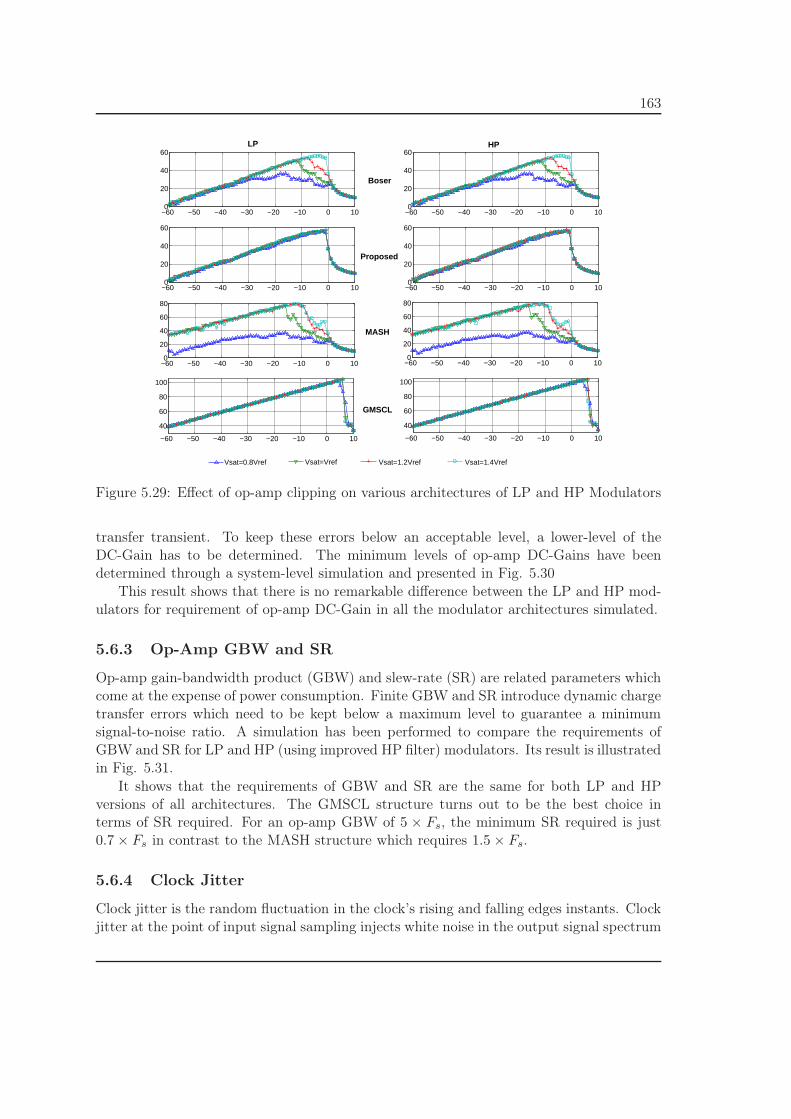
163
−60 −50 −40 −30 −20 −10 0 100
20
40
60
−60 −50 −40 −30 −20 −10 0 100
20
40
60
Vsat=0.8Vref Vsat=Vref Vsat=1.2Vref Vsat=1.4Vref
−60 −50 −40 −30 −20 −10 0 10
40
60
80
100
−60 −50 −40 −30 −20 −10 0 100
20
40
60
−60 −50 −40 −30 −20 −10 0 100
20
40
60
−60 −50 −40 −30 −20 −10 0 10
40
60
80
100
−60 −50 −40 −30 −20 −10 0 100
20
40
60
80
−60 −50 −40 −30 −20 −10 0 100
20
40
60
80
Proposed
MASH
Boser
LP HP
GMSCL
Figure 5.29: Effect of op-amp clipping on various architectures of LP and HP Modulators
transfer transient. To keep these errors below an acceptable level, a lower-level of theDC-Gain has to be determined. The minimum levels of op-amp DC-Gains have beendetermined through a system-level simulation and presented in Fig. 5.30
This result shows that there is no remarkable difference between the LP and HP mod-ulators for requirement of op-amp DC-Gain in all the modulator architectures simulated.
5.6.3 Op-Amp GBW and SR
Op-amp gain-bandwidth product (GBW) and slew-rate (SR) are related parameters whichcome at the expense of power consumption. Finite GBW and SR introduce dynamic chargetransfer errors which need to be kept below a maximum level to guarantee a minimumsignal-to-noise ratio. A simulation has been performed to compare the requirements ofGBW and SR for LP and HP (using improved HP filter) modulators. Its result is illustratedin Fig. 5.31.
It shows that the requirements of GBW and SR are the same for both LP and HPversions of all architectures. The GMSCL structure turns out to be the best choice interms of SR required. For an op-amp GBW of 5 × Fs, the minimum SR required is just0.7 × Fs in contrast to the MASH structure which requires 1.5 × Fs.
5.6.4 Clock Jitter
Clock jitter is the random fluctuation in the clock’s rising and falling edges instants. Clockjitter at the point of input signal sampling injects white noise in the output signal spectrum
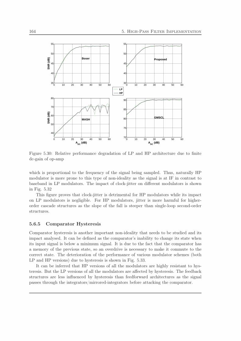
164 5. High-Pass Filter Implementation
0 10 20 30 40 50 6035
40
45
50
55
SN
R (
dB
)
0 10 20 30 40 50 6035
40
45
50
55
0 10 20 30 40 50 60
40
50
60
70
80
ADC
(dB)
SN
R (
dB
)
0 10 20 30 40 50 6070
75
80
85
90
ADC
(dB)
LP
HP
MASH
Boser Proposed
GMSCL
Figure 5.30: Relative performance degradation of LP and HP architecture due to finitedc-gain of op-amp
which is proportional to the frequency of the signal being sampled. Thus, naturally HPmodulator is more prone to this type of non-ideality as the signal is at IF in contrast tobaseband in LP modulators. The impact of clock-jitter on different modulators is shownin Fig. 5.32
This figure proves that clock-jitter is detrimental for HP modulators while its impacton LP modulators is negligible. For HP modulators, jitter is more harmful for higher-order cascade structures as the slope of the fall is steeper than single-loop second-orderstructures.
5.6.5 Comparator Hysteresis
Comparator hysteresis is another important non-ideality that needs to be studied and itsimpact analysed. It can be defined as the comparator’s inability to change its state whenits input signal is below a minimum signal. It is due to the fact that the comparator hasa memory of the previous state, so an overdrive is necessary to make it commute to thecorrect state. The deterioration of the performance of various modulator schemes (bothLP and HP versions) due to hysteresis is shown in Fig. 5.33.
It can be inferred that HP versions of all the modulators are highly resistant to hys-teresis. But the LP versions of all the modulators are affected by hysteresis. The feedbackstructures are less influenced by hysteresis than feedforward architectures as the signalpasses through the integrators/mirrored-integrators before attacking the comparator.

165
0.5 1 1.5 2 2.5 30
10
20
30
40
50
SN
DR
(d
B)
0.5 1 1.5 2 2.5 30
10
20
30
40
50
0.5 1 1.5 2 2.5 30
10
20
30
40
50
60
70
80
SR (xFs V/sec)
SN
DR
(d
B)
0.5 1 1.5 2 2.5 340
45
50
55
60
65
70
75
80
HPLP
SR (xFs V/sec)
GMSCL
Proposed
MASH
Boser
GBW=3× fs
GBW=5× fs
GBW=7× fs
GBW=3× fs
GBW=5× fs
GBW=7× fs
Figure 5.31: Impact of finite op-amp GBW and SR
0 1 2 3 4 530
35
40
45
50
55
SN
R (
dB
)
0 1 2 3 4 530
35
40
45
50
55
0 1 2 3 4 530
40
50
60
70
80
Jitter (% of Ts sec)
SN
R (
dB
)
0 1 2 3 4 530
40
50
60
70
80
90
100
Jitter (% of Ts sec)
LP
HP
Boser Proposed
MASH GMSCL
Figure 5.32: Clock jitter impact on modulator performance

166 5. High-Pass Filter Implementation
0 0.05 0.1 0.15 0.249
50
51
52
53
54
55
SN
R (
dB
)
0 0.05 0.1 0.15 0.248
49
50
51
52
53
54
55
0 0.05 0.1 0.15 0.240
50
60
70
80
90
Hysteresis (xVref V)
SN
R (
dB
)
0 0.05 0.1 0.15 0.230
40
50
60
70
80
90
Hysteresis (xVref V)
LP
HP
BoserProposed
MASH
GMSCL
Figure 5.33: Hysteresis
5.7 Conclusion
After carrying out different theoretical analyses and experimental tests over the three typesof HP Filters, it can be easily concluded that the improved filter is the best of the threestructures. It is least effected by the switch noise, opamp noise, parasitic capacitancesand consumes the least amount of power. It results in low distortion at high samplingfrequencies because of low capacitive load on the op-amp. Thus it can work at highsampling frequencies, which is essential in wide band converters. It keeps low frequencynoises away from the signal throughout the signal processing and filters white noise in a low-pass fashion, thus diminishing its power in the signal band near Fs/2. These characteristicsmake the improved filter an ideal choice for high-speed and high-resolution at reducedpower solution.
With the comparatove analysis between LP and HP modulators, it can be concludedthat the requirements on the performance of op-amp for both HP and LP modulators arethe same provided the improved version of HP filter is used. Clock jitter is detrimental tothe performance of HP modulator since the useful signal is in a high frequency region anda slight jitter in the clock introduces enormous errors in the sampled signal. Comparatorhysteresis on the other hand hits only the LP versions of the modulators except GMSLwhich has resistance against the hysteresis till 3% of Vref. All the architectures of HPmodulators are inherently robust in the face of comparator hysteresis.

167
Chapter 6
Design in 65nm CMOS
6.1 Introduction
The objective of this chapter is to provide the transistor level design of ADC which isdeveloped on system-level in the earlier chapters. This ADC is designed to satisfy theperformance requirements of the standards specified in Table. 6.1:
Looking at the diversity in performance requirements, it becomes evident that the ADChas to be reconfigurable. The reconfigurability is provided by changing sampling frequency(fs) and modulator order (M). In the GSM/EDGE mode, since the signal-bandwidthis small, 28.57MHz of fs (OSR = 28.57MHz
2×135KHz ≈ 105) and 2nd order noise-shaping withsingle bit quantizer is operated. Thus the second-stage of high-pass GMSCL structure isturned off in GSM/EDGE mode resulting in power saving. In the UMTS/WLAN modeof operation, the sampling frequency is elevated to 228.57MHz and the modulator orderis increased to 4 plus an additional stage of auxiliary quantizer. In this chapter, theop-amp system-level specifications are presented which provide a guide line for designingthe transistor-level op-amp. This is followed by the presentation of global single-endedcircuit in both GSM/EDGE and UMTS/WLAN modes of operation. Then, the individualbuilding blocks of the global circuit, including OTA, Comparator, DAC etc are exposed.Finally the simulation results are presented followed by the concluding remarks.
Standard GSM/EDGE UMTS WLANConversion Rate 270KHz 3.84MHz 25MHzSignal Bandwidth 135kHz 1.92MHz 12.5MHz
Sampling Frequency (fs) 28.57MHz 228.57MHz 228.57MHzModulator Order (P ) 2 4+aux. quantizer 4+aux. quantizer
SNR 80dB 80dB 52dB
Table 6.1: ADC Specification

168 6. Design in 65nm CMOS
6.2 System level specifications
The system-level specifications for the op-amp are derived in the previous chapter usingMATLAB. Based on the recommendations of the previous chapter, improved HP filter hasbeen selected for 65nm CMOS implementations. The specifications of the op-amp (dc-gain,gain-bandwidth product and slew rate) are presented in Fig. 6.1 based on the results ofthe previous chapter.
1 1.510 215 2.520 3250
30
5
35
10
40
15
45
20
50
25
55
30
60
35
38
40
40
45
42
50
44
55
46
48
50
52
Op−Amp Slew Rate (xFs V/sec)
54 GBW=5Fs
Op−Amp DC−Gain (dB)
SN
DR
(dB
)
Figure 6.1: DC Gain, GBW and SR specifications of the Op-Amp
As shown in this figure, the proposed modulator built with improved filter attains thedesired SNDR performance with an op-amp which has the minimum DC-gain of 30-dB,GBW of 5 × fs and SR of 1.8 × fs.
6.3 Global Circuit Schematic
The schematic of the modulator in the GSM mode is shown in its single-ended version forsimplicity in Fig. 6.2. Input switch of the modulator is bootstrapped to fulfill the linearityrequirements. The other switches are designed with CMOS transistors. The samplingcapacitance at the input of the modulator is chosen equal to 600fF to meet thermal noisespecifications.
The modulator used is of 2nd order with the architecture proposed in Chapter:5 anda 1 bit quantizer. This modulator provides the required SNDR performance at an OSR of84 as presented in the simulation results section. The size of the capacitors decreases withthe signal flow because of increased noise shaping along the signal path.
The single-ended modulator schematic in the ULAN mode is shown in Fig. 6.3. Itis the proposed-GMSCL structure with improved dynamic range by adding an auxiliaryquantizer in the last stage as described in Chapter 4.
The reference voltages used in the circuit are given in Table: 6.8.The OTA used in the first two high-pass filters has Miller configuration as shown in Fig.
6.4. This OTA was originally designed for the ADC published in [90]. It is a two-stageamplifier, with the first-stage providing the major portion of gain and the second-stage

169
−1
−1
−1
−1
+
−
+
− +
−
−1
Td
Sd
T
S
A
B
Sd
Td
1.125p
Sd
S
Sd
1.5p
Sd
V re f n1
inputOTA1
OTA2
Sd
T
Td S
T
Td
A B A B
A B A B
100f
600f450f
400f
T
45
0f
out put
T d
V re f p1
Figure 6.2: Single-ended global modulator in the GSM mode with its associated timingdiagram
acting as a buffer and providing voltage-swing. It is not a very power-efficient solution sinceboth the stages need to be biased with currents. The other drawback is that being two-stage amplifier, it needs capacitive compensation. But it provides reasonable performancefor Noise, DC-Gain, GBW and voltage-swing.
The OTA1 performance parameters are listed in Table. 6.2.
These parameters are obtained by using the component sizes mentioned in Tables. 6.3and 6.3. For the input differential pair, NMOS devices have been used. Such a configurationprovides a higher gain than the PMOS-input pair because of greater mobility of NMOSdevices [48]. The use of minimum-length transistors has been avoided in the input pairand in the current mirrors to limit 1/f noise and mismatching.
The common-mode feedback (CMFB) signal is provided by the switched-capacitor cir-cuit [91] shown in Fig. 6.5 which consumes negligible power.
Since the voltage-swing requirements are less stringent in the 3rd and 4th high-passfilters, gain-boosted Telescopic-Cascode OTA topology is the most-suitable for them. Ithas the advantages of less power consumption, high speed and high DC-Gain and thedisadvantage of low-voltage swing, which is not detrimental for the performance of thesefilters. This OTA topology is shown in Fig. 6.6.
The performance of this OTA configuration is summarized in Table. 6.5.
Like the previous OTA, the gain-boosted Telescopic OTA was also basically designedfor the low-pass ∆Σ ADC published in [90].

170 6. Design in 65nm CMOS
−1
−1
−1
−1
−
1
−1
−1
−1
+
−
+
− +
−
+
− +
−
+
−
+
−
−1
−1
100f
S
T d
100f
100f
Td
Td
100f
Sd
Td
1.125p
Sd
S
Sd
1.5p
Sd
inputOTA1
OTA2
Sd
T
Td S
T
Td
A B A B
A B A B
100f
600f450f
400f
Sd
Td
300f
OTA4
S
T
A B A B400f
200f
100f
100fSd
Sd
Sd
OTA3T
A B A B
300f
Sd
Sd
Sd
Sd
200f
Sd
50f
Sd
200f
Sd
Sd
Y1
Td
45
0f
Sd
Td
Y2 Σ
2b
Y3
Sd
Sd
Td
T d,Y2
V re f n1
V re f p1
V re f p1
V re f n1
V re f p1V re f p2V re f p3V re f p4V re f n4V re f n3V re f n2V re f n1
V re f n1
V re f p1
V re f p1
V re f n1
V re f n1
V re f p1
Vco
mp1
Vco
mp2
Vco
mp3
Td,Y
Td,Y1
V re f n1
V re f p1
Td,Y1
Td,Y2
Y
Td,−Y1
Td,−Y2
T d T d T d
50f50f50f
Figure 6.3: Single-ended global modulator in the UMTS/WLAN mode
Figure 6.4: OTA1 & OTA2 Configuration
6.4 Passive Adder
One of the principal advantages of using the proposed unity-STF structures is that it re-duces the constraints on the final adder before the quantizer and which can be implemented

171
OTA Parameters ValueInput/Output common mode 600mV
Input Voltage Swing 0.85VppOutput Voltage Swing +/- 350mV
DC Gain 41.3dBOpen Loop GBW 1049MHz
Phase Margin 64.6
Input Noise 36.7µVrmsSlew Rate 800V/µSec
Systematic Input Referred Offset 3mVCurrent consumption 8.2mA
Area 180µm×100µmPower Supply 1.2V
Process CMOS 65nm
Table 6.2: OTA1 Characteristics in integrating phase: Cs=0.6pF, Cint=1.25pF
Transistors Size UnitWidth Length
M1p, M1n 48 0.4 µmM2p, M2n 20 0.35 µmM3p, M3n 144 0.2 µmM4p, M4n 300 0.2 µm
Mcasp, Mcasn 20 0.2 µmMbias 480 1 µm
Table 6.3: Active components sizes in OTA1
Vout+
Vout−
Vcmc
AGND
AGND
Ccm f b1 Ccm f b2
Ccm f b2Ccm f b1
Vbias
Sd
Sd
Sd Td
Td
Td
Figure 6.5: CMFB Circuit
passively. The schematic of the passive adder is shown in Fig. 6.7.The expression for the output voltage Vs in case of null load capacitor, CL = 0, can be

172 6. Design in 65nm CMOS
Components Value UnitRzp, Rzn 250 Ω
CMp, CMn 320 fFCcmfb1 110 fFCcmfb2 55 fF
Table 6.4: Passive components values’ in OTA1
Figure 6.6: OTA3 & OTA4 Configuration
written as:
Vs =
∑2n=0 CanVan∑2
n=0 Can
=
∑2n=0 anCuVan∑2
n=0 anCu
(6.1)
where Van and Can are the input signal and capacitance of each branch respectively.The capacitance of each branch is proportional to the relative coefficient associated withit i-e an. For the symmetry purposes, unit capacitances Cu are used to implement Can.
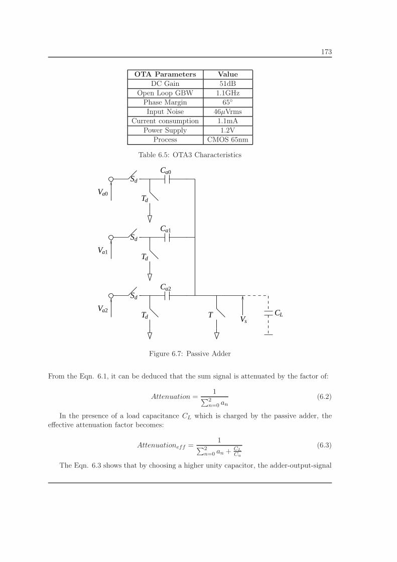
173
OTA Parameters ValueDC Gain 51dB
Open Loop GBW 1.1GHzPhase Margin 65
Input Noise 46µVrmsCurrent consumption 1.1mA
Power Supply 1.2VProcess CMOS 65nm
Table 6.5: OTA3 Characteristics
Ca2Sd
Td T
Ca1Sd
Td
Ca0Sd
Td
CLVa2
Va1
Va0
Vs
Figure 6.7: Passive Adder
From the Eqn. 6.1, it can be deduced that the sum signal is attenuated by the factor of:
Attenuation =1
∑2n=0 an
(6.2)
In the presence of a load capacitance CL which is charged by the passive adder, theeffective attenuation factor becomes:
Attenuationeff =1
∑2n=0 an + CL
Cu
(6.3)
The Eqn. 6.3 shows that by choosing a higher unity capacitor, the adder-output-signal
174 6. Design in 65nm CMOS
attenuation due to load capacitance is reduced. In the modulator circuit implmented asshown in Fig. 6.3, there is one passive adder in GSM mode and three passive adders inUMTS/ULAN mode. Since the output signal of the passive adders is fed to quantizers,the attenuation factor plays a role in defining the comparision reference voltages of thequantizer. The quantizer reference voltages are divided by the attenuation factors aswell. In the light of the attenuation factor associated with its passive adder, the four-levelquantizers’ comparison reference voltages are given in Table. 6.6.
Voltage Reference Adder Attenuation Value
Vcomp1 6 V REF4×6
Vcomp2 6 V REF2×6
Vcomp3 6 3×V REF4×6
Table 6.6: Four-Level Quantizer Voltage References
6.5 Quantizer
The four-level quantizer is used in the third stage of the modulator to achieve the requiredresolution. As discussed in Chapter:5, the multi-level quantizer at this stage introducesnegligible distortions. The four levels ADC is implemented as a flash quantizer with threecomparators in parallel as shown in Fig. 6.8.
The schematic of one individual comparator is shown in Fig. 6.5. A dynamic latch ischosen to save power since it consumes power only when performing latching function i-eduring one-half of the clock cycle. A wideband preamplifier improves latch sensitivity andisolates comparator input from kick-back noise. As the comparator should take a decisionwithin the non-overlap period between the clock phases, the latch must be very fast. Fora dynamic current of 140µA the latch delay is less than 500ps which is the worst case(clock=208MHz).
The values of different performance parameters of the comparator are compiled inTable. 6.5.
6.6 DAC
The global digital-to-analog-converter (DAC) is chosen depending on the value of the con-trol bit: ULAN as shown in Fig. 6.10. If the modulator is operating in GSM mode, theDAC operates on the single bit signal generated by the first-stage ADC. This DAC feed-backs either one of the reference voltages: V refp1, and V refn1. And, in UMTS/WLAN(ULAN) mode, the global DAC consists of the sum of three local DACs each of whichconverts the signal of its respective stage ADC.
Global DAC voltage references in both GSM and UMTS/ULAN modes of operationare mentioned in Table. 6.8 as the proportions of maximum DAC voltage-reference calledV ref .

175
+
−
+
−
+
− Sd
Td
Sd
Td
Sd
Td
D0
D1
D2
input
50f
50f
50f
Vcomp3
Vcomp2
Vcomp1
Figure 6.8: Four-level quantizer schematic
Figure 6.9: Comparator Configuration
6.7 Simulation results
The electrical simulation with real OTA (and associated CMFB circuit), quantizer, DACis succesfully performed for GSM mode. The output spectrum at full scale input is shown
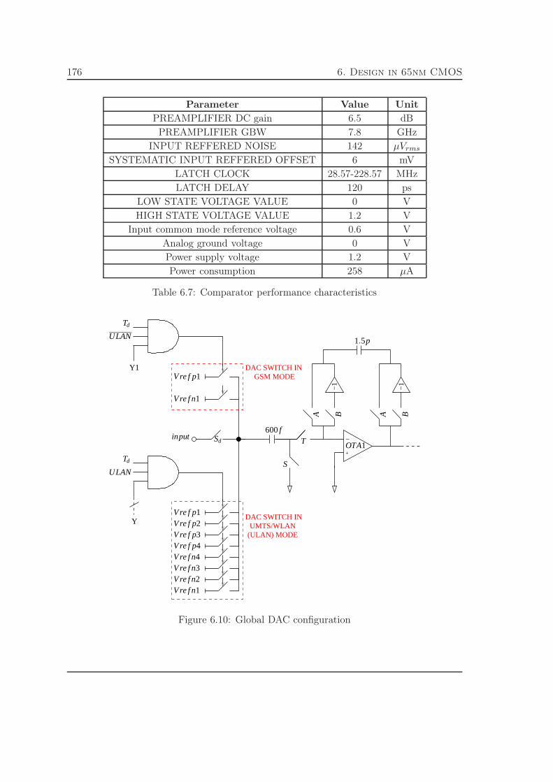
176 6. Design in 65nm CMOS
Parameter Value UnitPREAMPLIFIER DC gain 6.5 dBPREAMPLIFIER GBW 7.8 GHz
INPUT REFFERED NOISE 142 µVrms
SYSTEMATIC INPUT REFFERED OFFSET 6 mVLATCH CLOCK 28.57-228.57 MHzLATCH DELAY 120 ps
LOW STATE VOLTAGE VALUE 0 VHIGH STATE VOLTAGE VALUE 1.2 V
Input common mode reference voltage 0.6 VAnalog ground voltage 0 VPower supply voltage 1.2 VPower consumption 258 µA
Table 6.7: Comparator performance characteristics
−1
−1
+
−
DAC SWITCH INUMTS/WLAN
(ULAN) MODE
DAC SWITCH INGSM MODE
Y1
Y
S
1.5p
inputOTA1T
A B A B
600fSd
Td
Td
ULAN
ULAN
V re f p1
V re f n1
V re f p1V re f p2V re f p3V re f p4V re f n4V re f n3V re f n2V re f n1
Figure 6.10: Global DAC configuration

177
Voltage Reference GSM UMTS/WLAN
Vref1=Vrefp1-Vrefn1 Vref Vref
Vref2=Vrefp2-Vrefn2 - 3V ref4
Vref3=Vrefp3-Vrefn3 - V ref2
Vref4=Vrefp4-Vrefn4 - V ref4
Table 6.8: Global-DAC Voltage References
in Fig. 6.11. As presented in the figure, the resolution of 80-dB is achieved at the mini-mum OSR of 84 with the sampling frequency of 28.57MHz. Thus achieving the requiredspecification of GSM mode.
10−4
10−3
10−2
10−1
100
−100
−80
−60
−40
−20
0
20
Frequency (xFs Hz)
PS
D (
dB/H
z)
Fs=28.57MHz,Fin=14.18MHz,OSR=84,SNDR=80dB
fb
Figure 6.11: GSM mode simulation result
For the UMTS/WiFi modes of operation, an important distortion is observed in thesignal band. The clean simulation result of these modes is expected to be present in apossible extension of this research.
6.8 Conclusion
The transistor-level implementation of a multi-mode ADC working on the principle of high-pass delta-sigma modulation is presented. The ADC has two modes of operation namelyGSM/EDGE and UMTS/WLAN. This reconfigurability results in significant power saving.The implementation of key building blocks is presented in detail and their performanceparameters are tabled. The simulation result of GSM mode is presented with the specified

178 6. Design in 65nm CMOS
objectives achieved; while for the UMTS/WiFi modes, the clean simulation result withthe required linearity is still awaited and will be included in the future extensions of thisresearch work.

179
Chapter 7
Conclusion and Perspectives
7.1 Summary
The first part of this thesis presented the prominent radio receiver architectures whichare interesting for today’s wireless communication systems from the view point of recon-figurability, integrability and power consumption. An important step ahead towards theimplementation of the concept of SDR is RF sampling receivers which use subsamplingto bring down the signal from RF to IF. This way, the discrete time signal processingis introduced from the beginning, which is highly integrable. By using subsampling, thespeed requirements on the following blocks are relaxed. The challenge in this scenario isanti-alias filtering to minimize the corruption of the signal by in-band and out-of-bandinterferers. This is accomplished by passive switched-capacitor filters. The state-of-the-art receiver uses a two-stage downconversion, each stage using subsampling, to achieve anacceptable compromise between downconverted signal frequency and anti-alias filtering.Though, with the increase in performance of ADCs, it has become feasible to use single-stage downconversion to decrease the component count. The downsampling is carried outin such a way that the signal is placed at Fs/2 to enjoy the advantages of both zero-IF andlow-IF architectures. In this scenario, the natural candidate for ADC is HP ∆Σ modulator.
The second part of this thesis reviewed the state-of-the-art of ∆Σ modulators. Startingfrom the classical feed-back architectures, the recent state-of-the-art feed-forward architec-tures are discussed alongwith their pros and cons. Higher-order single-loop and multi-stagemodulators are also exposed which are inevitable for applications requiring high resolu-tion. System-level modeling of the classical second-order Boser modulator is carried outto demonstrate the requirements on op-amp for this topology.
The third part was related to the study of HP ∆Σ modulator. The HP ∆Σ modulatorshapes the quantization noise to low frequency. The signal band is located around one-halfof the sampling frequency, therefore it is compatible with Fs/2 IF discrete-time receiver and,in addition, completely immune to dc-offsets and flicker noise. Various existing topologiesof LP ∆Σ modulator are presented after adapting them for HP operation, and a new unity-STF single-loop second-order architecture is proposed. It alleviates the problems associatedwith traditional feedforward architecture by removing the need for an active summer. A

180 7. Conclusion and Perspectives
novel technique to design cascaded or MASH structures is also proposed which increasesthe input dynamic range of the modulator. This technique is based on the systematicstudy of the first-stage quantizer gain and the adaptation of digital cancellation filterswith this quantizer gain. An state-of-the-art architecture of multi-stage ∆Σ modulatorwhich is free from digital cancellation filters called Generalized-Multi-Stage-Closed-Loop(GMSCL) is adapted for HP operation while incorporating the proposed unity-STF single-loop architecture as its individual stage. Finally an auxiliary quantizer is added in thesecond-stage to increase the input dynamic range and to diminish the effect of the non-linearities of global feedback DAC. A study on the comparison between HP and LP ∆Σmodulators is also carried out, which reveals that the HP modulators are more sensitiveto clock jitter thereby increasing the constraints on the clock generation circuitry. LPmodulators on the other hand are increasingly sensitive to the hysteresis in the comparatornecessitating an scheme to reduce the requirements on the comparator.
The fourth part of this research was aimed at selecting the best architecture of HP filter,which is the basic building block of HP ∆Σ modulator. After a thorough comparativeanalysis of three competing topologies, the one which is recently introduced and basedon alternating capacitor positions is selected. Its advantages of reduced consumption andnoise are proved analytically and through simulations.
Finally a multi-standard, multi-mode ADC implementation in 65nm CMOS process ispresented. It has three modes of operation namely GSM, UMTS and WiFi/WiMax. InGSM mode, the proposed second-order HP ∆Σ modulator is used; while in UMTS andWiFi/WiMax modes, the double-loop, fourth-order, HP ∆Σ GMSCL structure with anauxiliary quantizer is used for conversion.
7.2 Perspectives
The idea of a single-stage subsampling-based downconversion receiver coupled with a pow-erful high-pass ∆Σ modulator needs to be rigorously studied and simulated. The challengein this context is the design of an efficient anti-aliasing filter, since there is only one stageof anti-aliasing which should also perform sufficient channel filtering. The alias rejectionof these filters needs to be augmented to achieve this objective. Since these subsamplingcircuits are implemented as SC circuits, they usually involve lot of high value capacitors.They occupy significant surface area, increase power consumption and do not scale withnew CMOS technologies. Thus, an innovative RF subsampling receiver architecture is nec-essary to reduce the capacitors count and size involved. Another problem associated withthese receiver architectures is the generation of high frequency clocks. New and innovativemethods of clock synthesization, which bring accuracy to the clock signals and minimizethe clock jitter noise, are to be developed.
For the GMSCL HP ∆Σ modulator, much better results in terms of power consump-tion and surface area can be obtained by using a feedback single-loop architecture in thesecond stage. The reason is that much power is consumed in charging the capacitors forfeedforward architectures which is not necassary because the second-stage only processesthe quantization noise of the first stage. A detailed system-level study is necessary to

181
design a GMSCL structure with feedfoward structure in the first stage and a feedbackstructure in the second stage.
Finally a multi-level comparator, digital adder and multi-level feedback DAC need tobe designed to properly exploit the idea of auxiliary quantizer which serves to minimize thenonlinearities generated by multi-level DAC. This way, even a larger spectrum of wirelessprotocols could be addressed with the ADC proposed.

182 7. Conclusion and Perspectives

183
Appendix A
Charge-Transfer Transient inIntegrator
In this annex, the charge transfer-transient of SC integrator is calculated. The influenceof op-amp finite DC-Gain and finite gain-bandwidth product is taken into account. Theimplementation of integrator in SC circuit along with its associated clocks is shown in Fig.A.1. It has to be noted that the charge-transfer occurs in the integration T phase.
−
+
Sd T
C1
C2
Td S
vinvout
S
T
n−1 n−1/2 n
Figure A.1: Integrator implementation in a SC circuit

184 A. Charge-Transfer Transient in Integrator
A.0.1 Phase S,n
In the sampling phase, the circuit configuration becomes as illustrated in Fig. A.2. ε is thevoltage on the negative terminal of the op-amp and is non-zero due to the non-ideal natureof the op-amp i-e having finite DC-Gain and GBW. ε is constant during the samplingphase and is equal to its value at the end of the preceding integration phase.
−
+
+ −
+−
vout
C1
C2
vin
ε Ao
Figure A.2: Circuit configuration in sampling phase
QC1= C1vin(nT )
QC2= C2(vout − ε)(nT )
A.0.2 Phase T,n-1/2
The circuit topology in the integration phase changes to as shown in Fig. A.3. Theobjective of this section is to find the charge transfer transient in this phase i-e to find theevolution of output voltage with time vout(t) as a function of the known parameters.
−
+
+ −
+−
vout(t)
C1
C2
ε(t) Ao
Figure A.3: Circuit configuration in charge-transfer phase
QC1(t) = −C1ε(t)

185
QC2(t) = C2 (vout(t) − ε(t))
By the law of conservation of charge:
QC1(t) + QC2
(t) = QC1(n − 1)T + QC2
(n − 1)T
−C1ε(t) + C2 (vout(t) − ε(t)) = C1vin(n − 1)T + C2(vout − ε)(n − 1)T
vout(t) =C1
C2ε(t) + ε(t) +
C1
C2vin(n − 1) − ε(n − 1)
=
(
1 +C1
C2
)
ε(t) +C1
C2vin(n − 1) + vout(n − 1) − ε(n − 1)
Assuming the single-pole op-amp model, and the relation of its input evolution ε(t)with its output vout(t), as presented in [92]:
ε(t) = − 1
Aovout(t) −
1
Aoσo
dvout(t)
dt
where Ao is the DC-Gain, σo is the pole radian frequency and Aoσo is the unity-gainradian frequency GBW of the op-amp. And also using the following approximation:
ε(n − 1) ≈ −vout(n − 1)
Ao
we get:
vout(t) =−(C2 + C1)
σo(AoC2 + C2 + C1)
dvout(t)
dt+
AoC2
AoC2 + C2 + C1
C1
C2vin(n − 1) +
AoC2 + C2
AoC2 + C2 + C1vout(n − 1)
=−(1 + b)
σo(Ao + 1 + b)
dvout(t)
dt+
Ao
Ao + 1 + b· b · vin(n − 1) +
Ao + 1
Ao + 1 + b· vout(n − 1)
where b = C1/C2 is the integrator gain. Using the approximation Ao + 1 + b ≃ Ao, weget:
vout(t) =−(1 + b)
σoAo
dvout(t)
dt+
Ao
Ao + 1 + b· b · vin(n − 1) +
Ao + 1
Ao + 1 + b· vout(n − 1)
Solving the differential equation, we get:
vout(t) = K · e−
σoAo
1 + b
!
t
+ α · b · vin(n − 1) + β · vout(n − 1) (A.1)
where:
α =Ao
Ao + 1 + b

186 A. Charge-Transfer Transient in Integrator
and:
β =Ao + 1
Ao + 1 + b
In Eqn. A.1 K is the constant which has to be found by the initial condition:
vout(0) = vout(n − 1) = K + α · b · vin(n − 1) + β · vout(n − 1)
⇒ K = vout(n − 1) − β · vout(n − 1) − α · b · vin(n − 1)
⇒ K ≈ −α · b · vin(n − 1)
Using this approximation in the Eqn. A.1, we have
vout(t) = β · vout(n − 1) + α · b · vin(n − 1)
1 − e
−
σoAo
1 + b
!
t
= β · vout(n − 1) + α · b · vin(n − 1)
1 − e
−
2πGBW
1 + b
!
t
(A.2)
Equation A.2 reveals that the time-constant of the integrator is:
τ =1 + b
2πGBW(A.3)

187
Appendix B
Charge-Transfer Transient inIntegrator-based HP Filter
In this annex, the charge transfer-transient of SC integrator-based HP filter is calculated.The influence of op-amp finite DC-Gain and finite gain-bandwidth product is taken intoaccount. The implementation of integrator in SC circuit along with its associated clocksis shown in Fig. B.1. It has to be noted that the charge-transfer occurs in the transfer Tphase.
+
−
−1
C3
C1
Sd T
T
Sd
S
Td
C2
Td S
vout
S
T
n−1 n−1/2 n
vin
Figure B.1: Integrator-based HP filter implementation
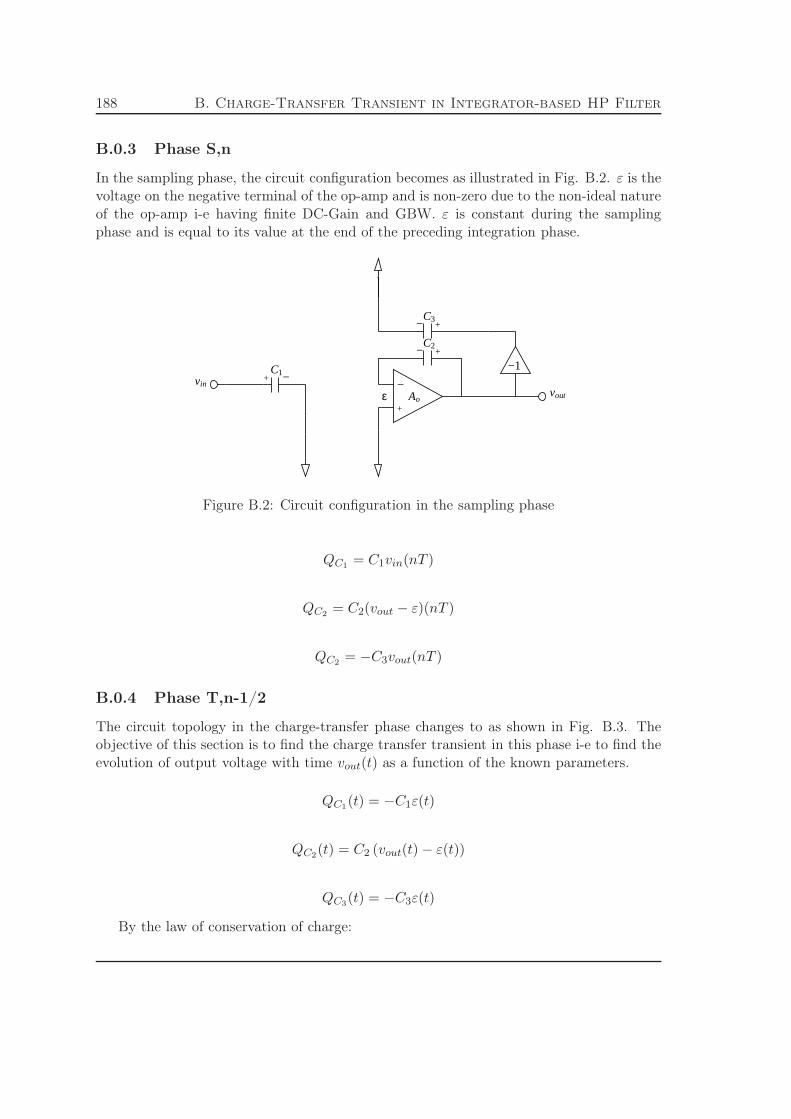
188 B. Charge-Transfer Transient in Integrator-based HP Filter
B.0.3 Phase S,n
In the sampling phase, the circuit configuration becomes as illustrated in Fig. B.2. ε is thevoltage on the negative terminal of the op-amp and is non-zero due to the non-ideal natureof the op-amp i-e having finite DC-Gain and GBW. ε is constant during the samplingphase and is equal to its value at the end of the preceding integration phase.
+
−1 + −
+−
+−
−
C2
C1
C3
vout
vin
ε Ao
Figure B.2: Circuit configuration in the sampling phase
QC1= C1vin(nT )
QC2= C2(vout − ε)(nT )
QC2= −C3vout(nT )
B.0.4 Phase T,n-1/2
The circuit topology in the charge-transfer phase changes to as shown in Fig. B.3. Theobjective of this section is to find the charge transfer transient in this phase i-e to find theevolution of output voltage with time vout(t) as a function of the known parameters.
QC1(t) = −C1ε(t)
QC2(t) = C2 (vout(t) − ε(t))
QC3(t) = −C3ε(t)
By the law of conservation of charge:
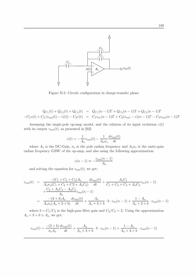
189
+
− + −
+−
− +
C2
C3
C1
vout(t)ε(t) Ao
Figure B.3: Circuit configuration in charge-transfer phase
QC1(t) + QC2
(t) + QC3(t) = QC1
(n − 1)T + QC2(n − 1)T + QC3
(n − 1)T
−C1ε(t) + C2 (vout(t) − ε(t)) − C3ε(t) = C1vin(n − 1)T + C2(vout − ε)(n − 1)T − C3vout(n − 1)T
Assuming the single-pole op-amp model, and the relation of its input evolution ε(t)with its output vout(t), as presented in [92]:
ε(t) = − 1
Aovout(t) −
1
Aoσo
dvout(t)
dt
where Ao is the DC-Gain, σo is the pole radian frequency and Aoσo is the unity-gainradian frequency GBW of the op-amp; and also using the following approximation:
ε(n − 1) ≈ −vout(n − 1)
Ao
and solving the equation for vout(t), we get:
vout(t) =−(C1 + C2 + C3)Ao
Aoσo(C1 + C2 + C3 + AoC2)
dvout(t)
dt+
AoC1
C1 + C2 + C3 + AoC2vin(n − 1)
+C2 + AoC2 − AoC3
Aovout(n − 1)
=−(3 + b)Ao
Aoσo(Ao + 3 + b)
dvout(t)
dt+
Ao
Ao + 3 + b· b · vin(n − 1) +
1 − Ao
Ao + 3 + b· vout(n − 1)
where b = C1/C2 is the high-pass filter gain and C3/C2 = 2. Using the approximationAo + 3 + b ≃ Ao, we get:
vout(t) =−(3 + b)
σoAo
dvout(t)
dt+
Ao
Ao + 3 + b· b · vin(n − 1) +
1 − Ao
Ao + 3 + b· vout(n − 1)
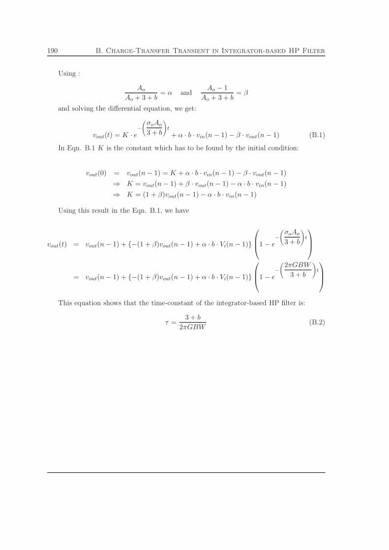
190 B. Charge-Transfer Transient in Integrator-based HP Filter
Using :
Ao
Ao + 3 + b= α and
Ao − 1
Ao + 3 + b= β
and solving the differential equation, we get:
vout(t) = K · e−
σoAo
3 + b
!
t
+ α · b · vin(n − 1) − β · vout(n − 1) (B.1)
In Eqn. B.1 K is the constant which has to be found by the initial condition:
vout(0) = vout(n − 1) = K + α · b · vin(n − 1) − β · vout(n − 1)
⇒ K = vout(n − 1) + β · vout(n − 1) − α · b · vin(n − 1)
⇒ K = (1 + β)vout(n − 1) − α · b · vin(n − 1)
Using this result in the Eqn. B.1, we have
vout(t) = vout(n − 1) + −(1 + β)vout(n − 1) + α · b · Vi(n − 1)
1 − e
−
σoAo
3 + b
!
t
= vout(n − 1) + −(1 + β)vout(n − 1) + α · b · Vi(n − 1)
1 − e
−
2πGBW
3 + b
!
t
This equation shows that the time-constant of the integrator-based HP filter is:
τ =3 + b
2πGBW(B.2)
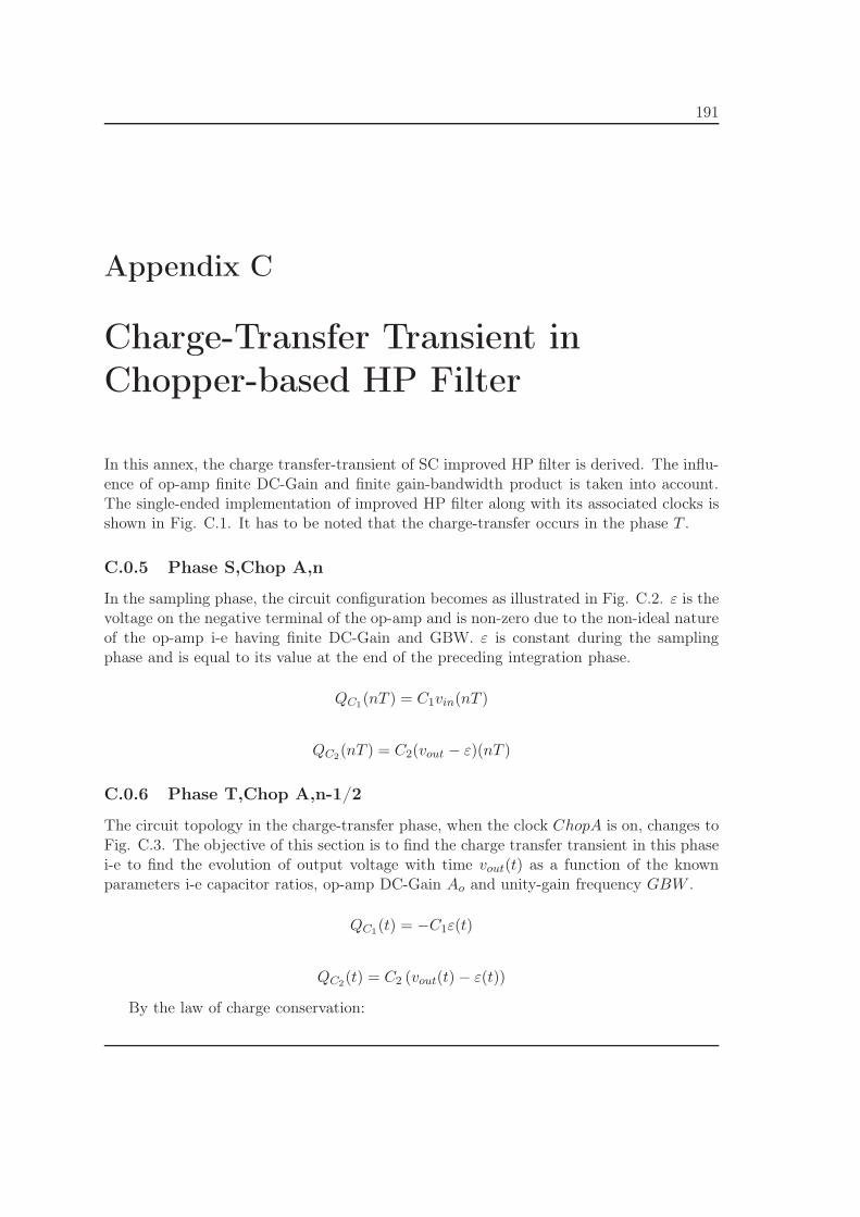
191
Appendix C
Charge-Transfer Transient inChopper-based HP Filter
In this annex, the charge transfer-transient of SC improved HP filter is derived. The influ-ence of op-amp finite DC-Gain and finite gain-bandwidth product is taken into account.The single-ended implementation of improved HP filter along with its associated clocks isshown in Fig. C.1. It has to be noted that the charge-transfer occurs in the phase T .
C.0.5 Phase S,Chop A,n
In the sampling phase, the circuit configuration becomes as illustrated in Fig. C.2. ε is thevoltage on the negative terminal of the op-amp and is non-zero due to the non-ideal natureof the op-amp i-e having finite DC-Gain and GBW. ε is constant during the samplingphase and is equal to its value at the end of the preceding integration phase.
QC1(nT ) = C1vin(nT )
QC2(nT ) = C2(vout − ε)(nT )
C.0.6 Phase T,Chop A,n-1/2
The circuit topology in the charge-transfer phase, when the clock ChopA is on, changes toFig. C.3. The objective of this section is to find the charge transfer transient in this phasei-e to find the evolution of output voltage with time vout(t) as a function of the knownparameters i-e capacitor ratios, op-amp DC-Gain Ao and unity-gain frequency GBW .
QC1(t) = −C1ε(t)
QC2(t) = C2 (vout(t) − ε(t))
By the law of charge conservation:

192 C. Charge-Transfer Transient in Chopper-based HP Filter
−1 −1 +
−
C2
ChopA
ChopB
ChopA
ChopB
vout
C1
Sd
Td S
vin
T
S
T
ChopA
ChopB
nn−1
n−1/2
Figure C.1: Improved HP filter implementation
−
+
+ −
+−
vout
C1
C2
vin
ε Ao
Figure C.2: Circuit configuration in the sampling phase, with ChopA clock on
QC1(t) + QC2
(t) = QC1(n − 1)T + QC2
(n − 1)T (C.1)
To find the charges stored in the capacitors during the phase S, n − 1, ChopB, pleaserefer to the Fig. C.4.
Looking at this figure, the charges stored at the end of (n − 1)th phase are evaluatedas:
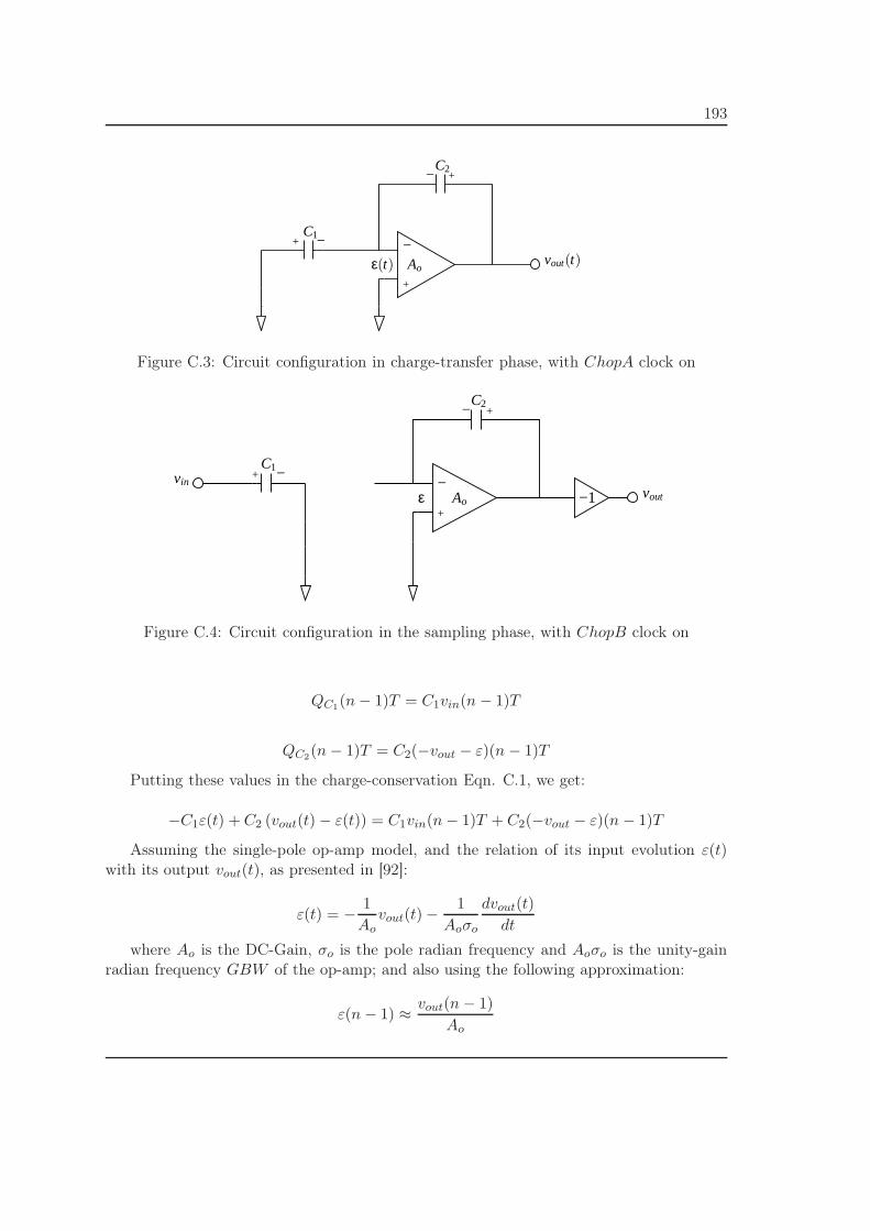
193
−
+
+ −
+−
vout(t)
C1
C2
ε(t) Ao
Figure C.3: Circuit configuration in charge-transfer phase, with ChopA clock on
−1 +
+ −
+−
−
C2
C1
ε Ao
vinvout
Figure C.4: Circuit configuration in the sampling phase, with ChopB clock on
QC1(n − 1)T = C1vin(n − 1)T
QC2(n − 1)T = C2(−vout − ε)(n − 1)T
Putting these values in the charge-conservation Eqn. C.1, we get:
−C1ε(t) + C2 (vout(t) − ε(t)) = C1vin(n − 1)T + C2(−vout − ε)(n − 1)T
Assuming the single-pole op-amp model, and the relation of its input evolution ε(t)with its output vout(t), as presented in [92]:
ε(t) = − 1
Aovout(t) −
1
Aoσo
dvout(t)
dt
where Ao is the DC-Gain, σo is the pole radian frequency and Aoσo is the unity-gainradian frequency GBW of the op-amp; and also using the following approximation:
ε(n − 1) ≈ vout(n − 1)
Ao

194 C. Charge-Transfer Transient in Chopper-based HP Filter
and solving the equation for vout(t), we get:
vout(t) =−(C1 + C2)Ao
Aoσo(C1 + C2 + AoC2)
dvout(t)
dt+
AoC1
C1 + C2 + AoC2vin(n − 1) − AoC2 + C2
Aovout(n − 1)
=−(1 + b)Ao
Aoσo(Ao + 1 + b)· dvout(t)
dt+
Ao
Ao + 1 + b· b · vin(n − 1) − Ao + 1
Ao + 1 + b· vout(n − 1)
where b = C1/C2 is the HP filter gain. Using the approximation Ao + 1 + b ≃ Ao, weget:
vout(t) =−(1 + b)
σoAo
dvout(t)
dt+
Ao
Ao + 1 + b· b · vin(n − 1) − Ao + 1
Ao + 1 + b· vout(n − 1)
Using :
Ao
Ao + 1 + b= α and
Ao + 1
Ao + 1 + b= β
and solving the differential equation, we get:
vout(t) = K · e−
σoAo
1 + b
!
t
+ α · b · vin(n − 1) − β · vout(n − 1) (C.2)
where K is the constant which has to be found by the initial condition:
vout(0) = −vout(n − 1) = K + α · b · vin(n − 1) − β · vout(n − 1)
⇒ K = −vout(n − 1) + β · vout(n − 1) − α · b · vin(n − 1)
⇒ K ≈ −α · b · vin(n − 1)
Using this approximation in the Eqn. C.2, we have
vout(t) = −β · vout(n − 1) + α · b · vin(n − 1)
1 − e
−
σoAo
1 + b
!
t
= −β · vout(n − 1) + α · b · vin(n − 1)
1 − e
−
2πGBW
1 + b
!
t
This equation shows that the time-constant of the Chopper-based HP filter is:
τ =1 + b
2πGBW(C.3)

195
Appendix D
Charge-Transfer Transient inImproved HP Filter
In this annex, the charge transfer-transient of SC improved HP filter is derived. The influ-ence of op-amp finite DC-Gain and finite gain-bandwidth product is taken into account.The single-ended implementation of improved HP filter along with its associated clocks isshown in Fig. D.1. It has to be noted that the charge-transfer occurs in the phase T .
D.0.7 Phase S,A,n
In the sampling phase, the circuit configuration becomes as illustrated in Fig. D.2. ε is thevoltage on the negative terminal of the op-amp and is non-zero due to the non-ideal natureof the op-amp i-e having finite DC-Gain and GBW. ε is constant during the samplingphase and is equal to its value at the end of the preceding integration phase.
QC1(nT ) = C1vin(nT )
QC2(nT ) = C2(vout − ε)(nT )
D.0.8 Phase T,Chop A,n-1/2
The circuit topology in the charge-transfer phase, when the clock ChopA is on, changes toFig. B.3. The objective of this section is to find the charge transfer transient in this phasei-e to find the evolution of output voltage with time vout(t) as a function of the knownparameters i-e capacitor ratios, op-amp DC-Gain Ao and unity-gain frequency GBW .
QC1(t) = −C1ε(t)
QC2(t) = C2 (vout(t) − ε(t))
By the law of charge conservation:

196 D. Charge-Transfer Transient in Improved HP Filter
−1
−1
+
−
Cho
pA
Cho
pB
Cho
pA
Cho
pB
T
S
T
ChopA
ChopB
nn−1
n−1/2
Sd
Td S
C2
C1vin
vout
Figure D.1: Improved HP filter implementation
−
+
+ −
+−
vout
C1
C2
vin
ε Ao
Figure D.2: Circuit configuration in the sampling phase, with ChopA clock on
QC1(t) + QC2
(t) = QC1(n − 1)T + QC2
(n − 1)T (D.1)
To find the charges stored in the capacitors during the phase S, n − 1, ChopB, please

197
−
+
+ −
+−
vout(t)
C1
C2
ε(t) Ao
Figure D.3: Circuit configuration in charge-transfer phase, with ChopA clock on
refer to the Fig. D.4.−
1
−1
+
− +
+−
− vin
C1
C2
voutAoε
Figure D.4: Circuit configuration in the sampling phase, with ChopB clock on
Looking at this figure, the charges stored at the end of (n − 1)th phase are evaluatedas:
QC1(n − 1)T = C1vin(n − 1)T
QC2(n − 1)T = C2(−vout + ε)(n − 1)T
Putting these values in the charge-conservation Eqn. D.1, we get:
−C1ε(t) + C2 (vout(t) − ε(t)) = C1vin(n − 1)T + C2(−vout + ε)(n − 1)T
Assuming the single-pole op-amp model, and the relation of its input evolution ε(t)with its output vout(t), as presented in [92]:
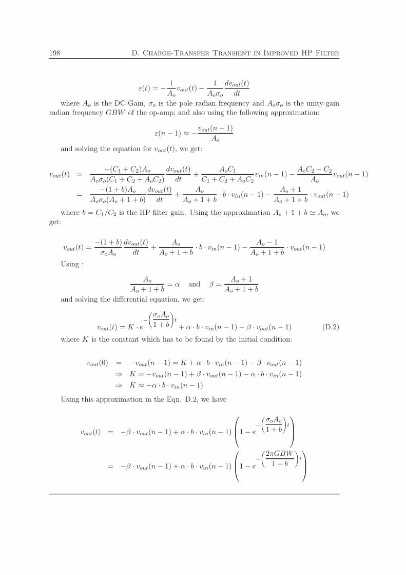
198 D. Charge-Transfer Transient in Improved HP Filter
ε(t) = − 1
Aovout(t) −
1
Aoσo
dvout(t)
dt
where Ao is the DC-Gain, σo is the pole radian frequency and Aoσo is the unity-gainradian frequency GBW of the op-amp; and also using the following approximation:
ε(n − 1) ≈ −vout(n − 1)
Ao
and solving the equation for vout(t), we get:
vout(t) =−(C1 + C2)Ao
Aoσo(C1 + C2 + AoC2)
dvout(t)
dt+
AoC1
C1 + C2 + AoC2vin(n − 1) − AoC2 + C2
Aovout(n − 1)
=−(1 + b)Ao
Aoσo(Ao + 1 + b)
dvout(t)
dt+
Ao
Ao + 1 + b· b · vin(n − 1) − Ao + 1
Ao + 1 + b· vout(n − 1)
where b = C1/C2 is the HP filter gain. Using the approximation Ao + 1 + b ≃ Ao, weget:
vout(t) =−(1 + b)
σoAo
dvout(t)
dt+
Ao
Ao + 1 + b· b · vin(n − 1) − Ao − 1
Ao + 1 + b· vout(n − 1)
Using :
Ao
Ao + 1 + b= α and β =
Ao + 1
Ao + 1 + b
and solving the differential equation, we get:
vout(t) = K · e−
σoAo
1 + b
!
t
+ α · b · vin(n − 1) − β · vout(n − 1) (D.2)
where K is the constant which has to be found by the initial condition:
vout(0) = −vout(n − 1) = K + α · b · vin(n − 1) − β · vout(n − 1)
⇒ K = −vout(n − 1) + β · vout(n − 1) − α · b · vin(n − 1)
⇒ K ≈ −α · b · vin(n − 1)
Using this approximation in the Eqn. D.2, we have
vout(t) = −β · vout(n − 1) + α · b · vin(n − 1)
1 − e
−
σoAo
1 + b
!
t
= −β · vout(n − 1) + α · b · vin(n − 1)
1 − e
−
2πGBW
1 + b
!
t

199
This equation shows that the time-constant of the improved HP filter is:
τ =1 + b
2πGBW(D.3)

200 D. Charge-Transfer Transient in Improved HP Filter

201
Bibliography
[1] A.S. Margulies and J. III. Mitola. Software defined radios: a technical challenge and amigration strategy. In Proceedings of the International Symposium on Spread SpectrumTechniques and Applications, volume 2, pages 551–556, 1998.
[2] K. Muhammad, R. B. Staszewski, and D. Leipold. Digital RF processing: toward low-cost reconfigurable radios. IEEE Communications Magazine, 43(8):105–113, August2005.
[3] A. Latiri. Architecture et conception de récepteur reconfigurable à échantillonnage RFpour les applications multistandard. PhD thesis, Telecom ParisTech, July 2008.
[4] L. Joet, A. Dezzani, F. Montaudon, F. Badets, F. Sibille, C. Corre, L. Chabert,R. Mina, F. Bailleuil, D. Saias, F. Paillardet, and E. Perea. Advanced ‘Fs/2’ discrete-time GSM receiver in 90-nm CMOS. In IEEE Asian Solid-State Circuits Conference,pages 371–374, November 2006.
[5] V. T. Nguyen. High-Pass ∆Σ Modulator and its Application to Time-Interleaved ∆ΣConverter. PhD thesis, Telecom ParisTech, 2004.
[6] V. T. Nguyen, P. Loumeau, and J. F. Naviner. High-pass ∆Σ modulator: from systemanalysis to circuit design. In Proceedings of the IEEE International Symposium onCircuits and Systems, June 2006.
[7] V.T. Nguyen, P. Desgreys, P. Loumeau, and J.F. Naviner. Noise analysis in high-pass∆Σ modulator. In Instrumentation and Measurement Technology Conference, 2006.IMTC 2006. Proceedings of the IEEE, pages 255–260, April 2006.
[8] V.T. Nguyen, P. Loumeau, and J.F. Naviner. Advantages of high-pass ∆Σ modula-tors in interleaved ∆Σ analog to digital converter. In Circuits and Systems, 2002.MWSCAS-2002. The 2002 45th Midwest Symposium on, volume 1, pages I–136–9vol.1, Aug. 2002.
[9] A. Latiri, L. Joet, P. Desgreys, and P. Loumeau. Passive second-order anti-aliasingfilter for RF sampling based receivers. Electronics Letters, 43(1):56–57, January 2007.
[10] Delta Sigma Data Converters: Theory, Design and Simulation. IEEE Press, IEEECircuits and Systems Society, 1997.

202 BIBLIOGRAPHY
[11] Y. Yasuda H. Inose and J. Murakami. A telemetering system by code modulation -∆−Σ modulation. IRE Transactions on Space Electronics and Telemetry, 8:204–209,September 1962.
[12] B. E. Boser and B. A. Wooley. The design of sigma-delta modulation and analog-to-digital converters. IEEE Journal of Solid-State Circuits, 23:1298–1308, December1988.
[13] J. Silva, U. Moon, J. Steensgaard, and G.C Temes. Wideband low-distortion delta-sigma ADC topology. Electronics Letters, 44(8), April 2008.
[14] M. Oberst and R. Weigel. Delta-Sigma feedforward topology. Electronics Letters,37(12):737–738, June 2001.
[15] V. T. Nguyen, P. Loumeau, and H. Fakhoury. Convertisseur sigma-delta. EuropeanPatent, December 2008. Number: FR 08/58632.
[16] V. T. Nguyen, P. Loumeau, and P. Benabes. Convertisseur sigma-delta. EuropeanPatent, May 2008. Number: FR 08/53213.
[17] N. Maghari, S. Kwon, G.C. Temes, and U. Moon. Sturdy MASH ∆ − Σ modulator.Electronics Letters, 42(22):1269–1270, October 2006.
[18] G. Cauwenberghs and G. C. Temes. Adaptive calibration of multiple quantizationoversampled A/D converters. In Proceedings of the IEEE International Symposiumon Circuits and Systems, volume 1, pages 512–515, May 1996.
[19] G. Cauwenberghs and G. C. Temes. Adaptive digital correction of analog errors inmash ADC’s-part I: Off-line and blind on-line calibration. IEEE Transactions onCircuits and Systems-II:Analog and Digital Signal Processing, 47(7):621–628, July2000.
[20] Y. Yang, R. Shreier, G. C. Temes, and S. Kiaei. On-line adaptive digital correctionof dual-quantization delta-sigma modulators. Electronics Letters, 28(16):1511–1513,1992.
[21] S. Abdennadher, S. Kiaei, G. C. Temes, and R. Shreier. Adaptive self-calibratingdelta-sigma modulators. Electronics Letters, 28(14):1288–1289, 1992.
[22] A. Wiesbauer and G. C. Temes. Adaptive digital compensation of analog circuit imper-fections for cascaded ∆Σ modulators. In Proceedings of the 30th Asilomar Conferenceon Signals, Systems and Computers, November 1996.
[23] G. Cauwenberghs. Blind on-line digital calibration of multi-stage nyquist-rate andoversampled A/D converters. IEEE Transactions on Circuits and Systems-II:Analogand Digital Signal Processing, 1:401–404, 1998.
203
[24] P. Kiss, J. Silva, A. Wiesbauer, T. Sun, U. K. Moon, J. T. Stonick, and G. C. Temes.Adaptive digital correction of analog errors in mash adc’s-part ii: Correction usingtest-signal injection. IEEE Transactions on Circuits and Systems-II:Analog and Dig-ital Signal Processing, 47(7):629–638, July 2000.
[25] P. Benabes, A. Gauthier, and R. Kielbasa. New high-order universal ∆Σ modulator.Electronics Letters, 31(1):8–9, January 1995.
[26] N. Maghari, G.C. Temes, and U. Moon. Single-loop ∆Σ modulator with extendeddynamic range. Electronics Letters, 44(25):1452–1453, December 2008.
[27] A. K. Ong and B. A. Wooley. A Two-Path Bandpass Σ∆ Modulator for DigitalIF Extraction at 20 MHz. IEEE Journal of Solid-State Circuits, 32(12):1920–1934,December 1997.
[28] A. Tabatabaei and B.A. Wooley. A Wideband Bandpass Sigma-Delta Modulator forWireless Applications. In Symposium on VLSI Circuits, 1999. Digest of TechnicalPapers., pages 91–92, June 1999.
[29] I. V. O’Connell and C. Lyden. A high pass switched capacitor Σ∆ modulator. In Inter-national Conference on Electronics, Circuits and Systems, pages 307–310, September2002.
[30] V.T. Nguyen, P. Loumeau, and J.F. Naviner. An interleaved delta-sigma analog todigital converter with digital correction. In Acoustics, Speech, and Signal Processing,2002. Proceedings. (ICASSP ’02). IEEE International Conference on, volume 4, pagesIV–4193 vol.4–, 2002.
[31] B. Razavi. Design considerations for direct-conversion receivers. IEEE Transactionson Circuits and Systems II: Analog and Digital Signal Processing, 44(6):428–435, June1997.
[32] R. Hartley. Single-sideband modulator. U.S Patent 1 666 206, April 1928.
[33] D. K. Weaver. A third method of generation and detection of single sideband signals.Proc. IRE, 44:1703–1705, 1956.
[34] A. Hairapetian. An 81MHz IF receiver in CMOS. In Proceedings of the IEEE Inter-national Solid-State Circuits Conference, pages 56–57, February 1996.
[35] J. E. Eklund and R. Arvidsson. A 10b 120 MS/s multiple sampling single conversionCMOS A/D converter for I/Q demodulation. In Proceedings of the IEEE InternationalSolid-State Circuits Conference, pages 294–295, February 1996.
[36] S. Jantzi, K. Martin, and A. Sedra. A quadrature bandpass ∆Σ modulator for digitalradio. In Proceedings of the IEEE International Solid-State Circuits Conference, pages126–127, February 1997.

204 BIBLIOGRAPHY
[37] A. A. Abidi. Direct-conversion radio transceivers for digital communications. IEEEJournal of Solid-State Circuits, 30:1399–1410, December 1995.
[38] I. A. W. Vance. Fully integrated radio paging receiver. IEE Proceedings on Commu-nications, Radar and Signal Processing, 129(1):2–6, February 1982.
[39] J. F. Wilson, R. Youell, T. H. Richards, G. Luff, and R. Pilaski. A single-chip VHFand UHF receiver for radio paging. IEEE Journal of Solid-State Circuits, 26(12):1944–1950, December 1991.
[40] A. Bateman and D. M. Haines. Direct conversion transceiver design for compact low-cost portable mobile radio terminals. In Proceedings of the IEEE Vehicular Conference,pages 57–62, 1989.
[41] S. A. Jantzi, K. Martin, M. Snelgrove, and A. S. Sedra. A complex bandpass ∆Σconverter for digital radio. In Proceedings of the IEEE International Symposium onCircuits and Systems, volume 5, pages 453–456, May 1994.
[42] J. Crols and M. S. J. Steyaert. A single-chip 900MHz cmos receiver front-end witha high performance low-IF topology. IEEE Journal of Solid-State Circuits, 30:1483–1492, December 1995.
[43] P. R. Gray. Architectures and technologies for cmos RF transceivers. In IEEE Inter-national Solid-State Circuits Conference, Short Course: RF cmos circuit design forPersonal Communication Systems, pages 453–456, February 1997.
[44] Yi-Ran Sun and S. Signell. A generalized quadrature bandpass sampling in radioreceivers. In Proceedings of the Asia and South Pacific Design Automation ConferenceASP-DAC, volume 2, pages 1288–1291, 2005.
[45] T. Riley S. Karvonen and J. Kostamovaara. A hilbert sampler/filter and complexbandpass SC filter for I/Q demodulation. In Proceedings of the 26th European Solid-State Circuits Conference, ESSCIRC, pages 280–283, 2000.
[46] R.G. Vaughan, N.L. Scott, and D.R. White. The theory of bandpass sampling. IEEETransactions on Signal Processing, 39(9):1973–1984, September 1991.
[47] Qizheng Gu. RF System Design of Transceivers for Wireless Communications.Springer-Verlag New York, Inc., Secaucus, NJ, USA, 2006.
[48] Behzad Razavi. RF microelectronics. Prentice-Hall, Inc., Upper Saddle River, NJ,USA, 1998.
[49] H. Pekau and J.W. Haslett. Cascaded noise figure calculations for radio receiver cir-cuits with noise-aliasing properties. IEE Proceedings on Circuits, Devices and Systems,153(6):517–524, 2006.

205
[50] F. Montaudon, R. Mina, S. L. Tual, L. Joet, D. Saias, R. Hossain, F. Sibille, C. Corre,V. Carrat, E. Chataigner, J. Lajoinie, S. Dedieu, F. Paillardet, and E. Perea. Ascalable 2.4-to-2.7ghz wi-fi/wimax discrete-time receiver in 65nm cmos. In Proceedingsof the IEEE International Solid-State Circuits Conference, pages 362–619, February2008.
[51] 3GPP. Digital cellular telecommunications system (phase2+);radio transmission andreception (3gpp ts 45.005). Ts, 3GPP, April 2006.
[52] Oversampling Delta-Sigma Converters. IEEE Press, 1992.
[53] Top-Down Design of High-Performance Sigma-Delta Modulators. Kluwer AcademicPublishers, 1999.
[54] R. M. Gray. Quantization noise spectra. IEEE Transactions on Information Theory,36:1220–1244, November 1990.
[55] A. Rusu, B. R. Jose, M. Ismail, and H. Tenhunen. A dual-band sigma-delta modulatorfor GSM/WCDMA receivers. In DCIS 2004, Bordeaux, France, June 2004.
[56] W. L. Lee and C. G. Sodini. A topology for higher order interpolative coders. InProceedings of the IEEE International Symposium on Circuits and Systems, pages459–462, 1987.
[57] Z. Lin and W. Sheu. A generic multiple-feedback architecture and method for thedesign of high-order Σ − ∆ modulators. IEEE Transactions on Circuits and SystemsII: Analog and Digital Signal Processing, 49:465–473, July 2002.
[58] Y. Yin, H. Klar, and P. Wennekers. A novel broadband cascaded sigma-delta analog-to-digital converter. In Proceedings of the IASTED International Conference on Cir-cuits, Signals, and Systems, pages 86–91, 2004.
[59] P. Benabes, A. Gauthier, and D. Billet. New wideband sigma-delta convertor. Elec-tronics Letters, 29(17):1575–1577, August 1993.
[60] Understanding Delta-Sigma Data Converters. IEEE Press, IEEE Circuits and SystemsSociety, 2005.
[61] P. Balmelli and Q. Huang. A 25MS/s 14b 200mW Σ−∆ Modulator in 0.18µm CMOS.IEEE Journal of Solid-State Circuits, 39(12):74–75, December 2004.
[62] Louis A. Williams and Bruce A. Wooley. Third-order cascaded sigma-delta modula-tors. IEEE Transactions on Circuits and Systems, 38(5), May 1991.
[63] R. T. Baird and T. S. Fiez. Improved ∆Σ DAC linearity using data weighted aver-aging. In Proceedings of the IEEE International Symposium on Circuits and Systems,volume 1, pages 13–16, 1995.

206 BIBLIOGRAPHY
[64] I. Fujimori, L. Longo, A. Hairapetian, K. Seiyama, S. Kosic, C. Jun, and S. L. Chan. A90dB SNR 2.5MHz output-rate ADC using cascaded multibit delta-sigma modulationat 8x oversamling ratio. IEEE Journal of Solid-State Circuits, 35(12):1820–1828,December 2000.
[65] F. Chen and B. H. Leung. A high resolution multibit sigma-delta modulator withindividual level averaging. IEEE Journal of Solid-State Circuits, 30(4):453–460, April1995.
[66] R. Schreier and B. Zhang. Noise-shaped multibit D/A convertor employing unit ele-ments. Electronics Letters, 31(20):1712–1713, September 1995.
[67] I. I. Galton. Spectral shaping of circuit errors in digital-to-analog converters. IEEETransactions on Circuits and Systems II, 44:808–817, October 1997.
[68] M. S. Nejad and G. C. Temes. A high-resolution multi-bit Σ∆ ADC with digitalcorrection and relaxed amplifier requirements. IEEE Journal of Solid-State Circuits,28:648–660, June 1993.
[69] J. Silva, X. Wang, P. Kiss, U. Moon, and G. C. Temes. Digital techniques for im-proved ∆Σ data conversion. In Proceedings of the IEEE Custom Integrated CircuitsConference, pages 183–190, May 2002.
[70] B. P. Brandt and B. A. Wooley. A 50-MHz multibit sigma-delta modulator for 12-b 2-MHz A/D conversion. IEEE Journal of Solid-State Circuits, 26(12):1746–1756,December 1991.
[71] J. C. Candy. A use of double integration in sigma-delta modulation. IEEE Transac-tions on Communication, COM-33(3):249–258, March 1985.
[72] L. J. Breems, R. Rutten, and G. Wetzker. A cascaded continuous-time sd modulatorwith 67-db dynamic range in 10-mhz bandwidth. IEEE Journal of Solid-State Circuits,39(12):2152–2160, December 2004.
[73] R. Schoofs, M. S. J. Steyaert, and W. M. C. Sansen. A design-optimized continuous-time delta-sigma ADC for WLAN applications. IEEE Transactions on Circuits andSystems I: Regular Papers, 54(1):209–217, January 2007.
[74] A. Di Giandomenico, S. Paton, A. Wiesbauer, L. Hernandez, T. Potscher, and L. Dor-rer. A 15 MHz bandwidth sigma-delta ADC with 11 bits of resolution in 0.13 µm cmos.In IEEE European Solid-State Circuits Conference, pages 233–236, 2003.
[75] G. Mitteregger, C. Ebner, S. Mechnig, T. Blon, C. Holuigue, and E. Romani. A 20-mw 640-MHz CMOS continuous-time Σ∆ ADC with 20-MHz signal bandwdith, 80-dBdynamic range and 12-bit ENOB. IEEE Journal of Solid-State Circuits, 41(12):2641–2649, December 2006.

207
[76] S.D. Kulchycki, R. Trofin, K. Vleugels, and B.A. Wooley. A 77-dB dynamic range,7.5-MHz hybrid continuous-time/discrete-time cascaded Σ∆ modulator. Solid-StateCircuits, IEEE Journal of, 43(4):796–804, April 2008.
[77] H. H. Tao, L. Toth, and J. M. Khoury. Analysis of timing jitter in bandpass sigma-delta modulators. IEEE Transactions on Circuits and Systems II, 46:991–1001, August1999.
[78] P. Malcovati, S. Brigati, F. Francesconi, F. Maloberti, P. Cusinato, and A. Baschirotto.Behavioral modeling of switched-capacitor sigma-delta modulators. Circuits and Sys-tems I: Fundamental Theory and Applications, IEEE Transactions on, 50(3):352–364,Mar 2003.
[79] C. C. Enz and G. C. Temes. Circuit techniques for reducing reducing the effects of op-amp imperfections: autozeroing, correlated double sampling and chopper stabilization.Proceedings IEEE, 46:991–1001, August 1999.
[80] H. Zare-Hoseini, I. Kale, and O. Shoaei. Modeling of switched-capacitor delta-sigmamodulators in simulink. Instrumentation and Measurement, IEEE Transactions on,54(4):1646–1654, Aug. 2005.
[81] F. Medeiro, B. Perez-Verdu, A. Rodriguez-Vazquez, and J.L. Huertas. Modelingopamp-induced harmonic distortion for switched-capacitor Σ∆ modulator design. InCircuits and Systems, 1994. ISCAS ’94., 1994 IEEE International Symposium on,volume 5, pages 445–448 vol.5, May-2 Jun 1994.
[82] Analog MOS Integrated Circuits. John Wiley and Sons, New York, 1986.
[83] C. C. Enz and G. C. Temes. Circuit techniques for reducing the effects of op-ampimperfections: autozeroing, correlated double sampling, and chopper stabilization.Proceedings of the IEEE, 84(11):1584–1614, November 1996.
[84] K. C. Hsieh, P. R. Gray, D. Senderowicz, and D. G. Messerschmitt. A low-noisechopper-stabilized differential switched-capacitor filtering technique. IEEE Journal ofSolid-State Circuits, 16(6):708–715, December 1981.
[85] L. Toth and Y. P. Tsividis. Generalization of the principle of chopper stabilization.IEEE Transactions on Circuits and Systems I: Fundamental Theory and Applications,50(8):975–983, August 2003.
[86] H. Petit and J. F. Naviner. Modèle linéaire de quantificateur pour la synthèse demodulateur sigma-delta cascade. In TAISA, 2001.
[87] P.K Singh and F. Maloberti. Design Considerations for Band-pass Sigma-Delta Modu-lators. In Proceedings of the IEEE International Symposium on Circuits and Systems,volume 1, pages 336–339, 2001.
208 BIBLIOGRAPHY
[88] Y. Dong and A. Opal. Time-Domain Thermal Noise Simulation of Switched CapacitorCircuits and Delta-Sigma Modulators. IEEE Transactions On Computer-Aided DesignOf Integrated Circuits And Systems, 19(4):473–481, April 2000.
[89] J. Kasdin. Discrete Simulation of Colored Noise and Stochastic Processes and 1/fα;Power Law Noise Generation. The Proceedings of the IEEE, 83(5):802–827, May 1995.
[90] H. Fakhoury, C. Jabbour, H. Khushk, V. T. Nguyen, and P. Loumeau. A 65nmCMOS EDGE/UMTS/WLAN tri-mode four-channel time-interleaved ∆Σ ADC. InProceedings of the IEEE International Symposium on Circuits and Systems, volume 1,pages 336–339, 2001.
[91] A. N. Karanicolas, K. O. Kenneth, and J. Y. Wang. A high-frequency fully differentialbicmos operational amplifier. IEEE Journal of Solid-State Circuits, 26(3):203–208,March 1991.
[92] G.C. Temes. Finite amplifier gain and bandwidth effects in switched-capacitor filters.Solid-State Circuits, IEEE Journal of, 15(3):358–361, Jun 1980.