
Modular High Power Solid State RF Amplifiers for Particle ...
Microwave Networks-1
JHW 5/12/2011
MIT Lincoln Laboratory
Modular System RF Design*
“Build Your Own Small Radar System...”
2011 MIT Independent Activities Period (IAP)
*This work is sponsored by the Department of the Air Force under Air Force Contract #FA8721-05-C-0002. Opinions,
interpretations, conclusions and recommendations are those of the authors and are not necessarily endorsed by the
United States Government.
Jonathan H. Williams
MIT Lincoln Laboratory
January 2011
MIT Lincoln LaboratoryRF Modular Design IAP
2
JHW 5/12/2011
• Introduction
• Circuit and Network Theory
• RF Measurements
• RF Design/Build
• Summary
Outline

MIT Lincoln LaboratoryRF Modular Design IAP
3
JHW 5/12/2011
RF Design Requirements
Design Parameters
• Frequency = 2.4GHz
• BW = 80MHz
• Waveform = CW Ramp
• Antenna Isolation = 50dB
• DC Power < 1 Watt
• RF Power < 1 Watt (EIRP)
Realization Constraints
• Use off the shelf parts
• Use connectorized components
• Minimal soldering
• Use AA batteries
Functional Decomposition
• Transmitter
– Modulated source
– Amplification
– Distribution
– Antenna for radiation
• Receiver
– Antenna receive aperture
– Amplification
– De-modulate
– Frequency Translate

MIT Lincoln LaboratoryRF Modular Design IAP
4
JHW 5/12/2011
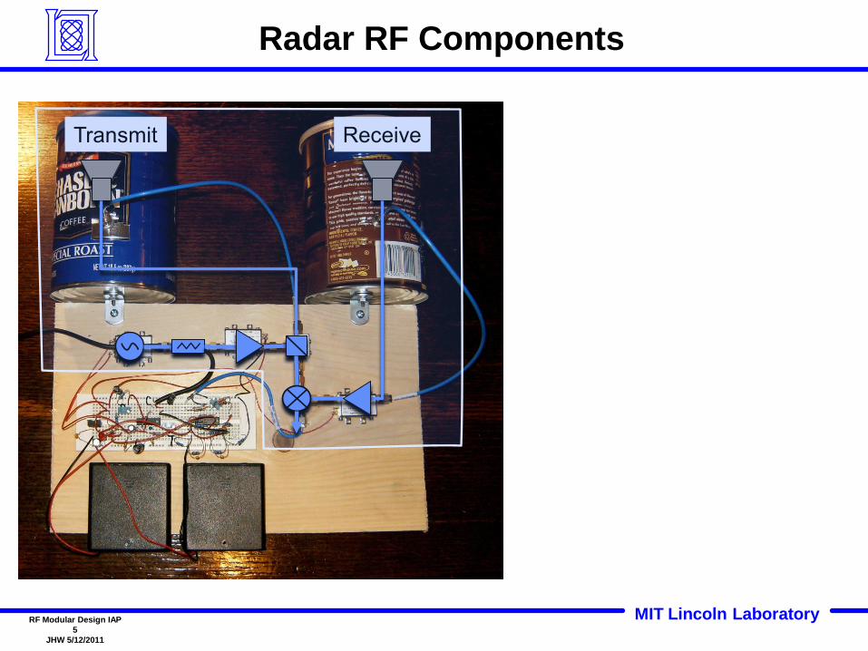
Radar RF Components
Transmit Receive
MIT Lincoln LaboratoryRF Modular Design IAP
5
JHW 5/12/2011
Radar RF Components
Transmit Receive
MIT Lincoln LaboratoryRF Modular Design IAP
6
JHW 5/12/2011
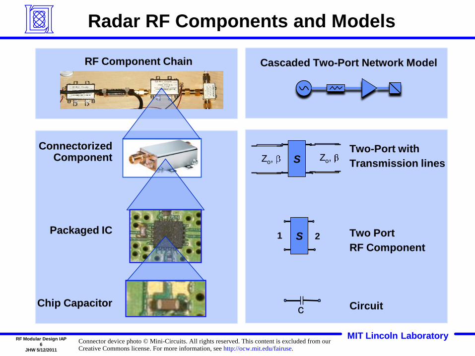
Radar RF Components and Models
ConnectorizedComponent
Packaged IC
Chip Capacitor
RF Component Chain Cascaded Two-Port Network Model
Two-Port with
Transmission lines
Two Port
RF Component
Circuit
S1 2
c
SZo, Zo,
Connector device photo © Mini-Circuits. All rights reserved. This content is excluded from ourCreative Commons license. For more information, see http://ocw.mit.edu/fairuse.
MIT Lincoln LaboratoConnector device photo © Mini-Circuits. All rights reserved. This content is excluded from ourCreative Commons license. For more information, see http://ocw.mit.edu/fairuse.
ryRF Modular Design IAP
7
JHW 5/12/2011
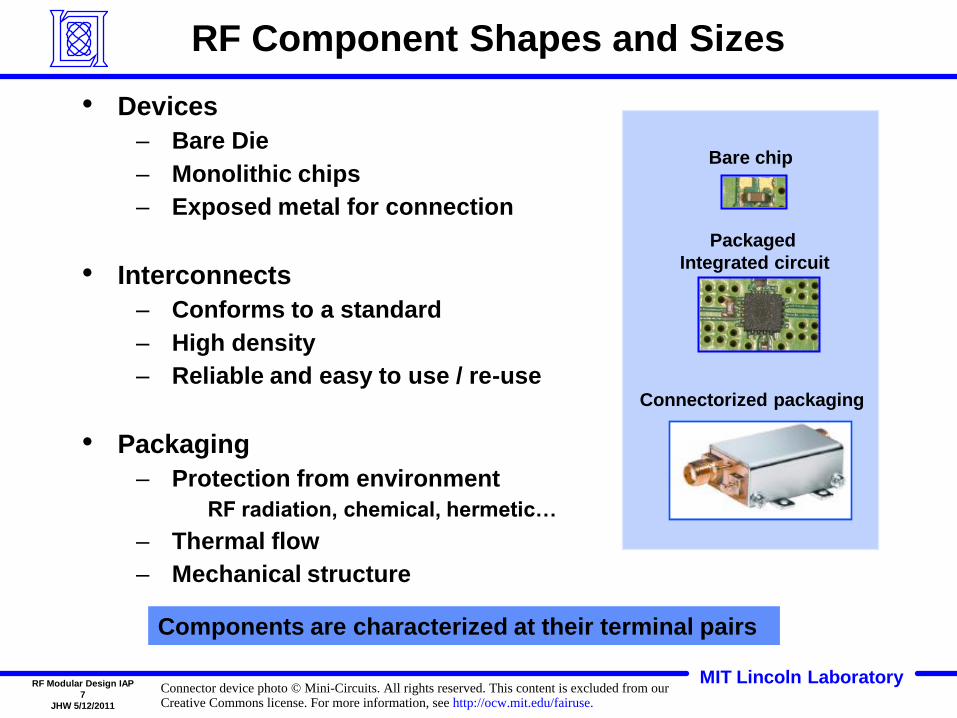
RF Component Shapes and Sizes
• Devices
– Bare Die
– Monolithic chips
– Exposed metal for connection
• Interconnects
– Conforms to a standard
– High density
– Reliable and easy to use / re-use
• Packaging
– Protection from environment
RF radiation, chemical, hermetic…
– Thermal flow
– Mechanical structure
Bare chip
Connectorized packaging
Packaged
Integrated circuit
Components are characterized at their terminal pairs
MIT Lincoln LaboratoryRF Modular Design IAP
8
JHW 5/12/2011
Circuit and RF Component Models
• Circuit components
– Component behavior is described at the terminals
– Using a current-voltage relationship
– Components are connected with ideal lines to form a circuit
– Circuit theory used to determine overall circuit behavior
• RF components
– Component behavior is described at terminal pair ports
– Using scattering parameters
– Components are connected by transmission lines
– Network theory used to determine overall behavior
Circuit Model
Two Port Network Model
c
S
3 Port Network Model
S1
23
1 2
Connector device photo © Mini-Circuits. All rights reserved. This content is excluded from ourCreative Commons license. For more information, see http://ocw.mit.edu/fairuse.

MIT Lincoln LaboratoryRF Modular Design IAP
9
JHW 5/12/2011
• Introduction
• Circuit and Network Theory
• RF Measurements
• RF Design/Build
• Summary
Outline
MIT Lincoln LaboratoryRF Modular Design IAP
10
JHW 5/12/2011
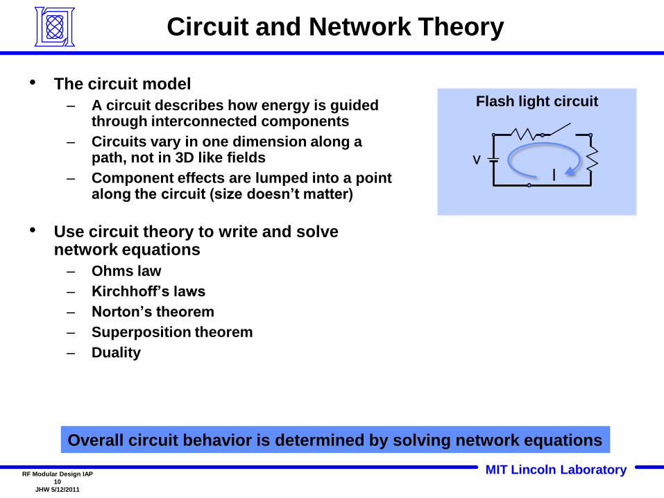
Circuit and Network Theory
• The circuit model
– A circuit describes how energy is guided through interconnected components
– Circuits vary in one dimension along a path, not in 3D like fields
– Component effects are lumped into a point along the circuit (size doesn’t matter)
• Use circuit theory to write and solve network equations
– Ohms law
– Kirchhoff’s laws
– Norton’s theorem
– Superposition theorem
– Duality
Flash light circuit
vI
Overall circuit behavior is determined by solving network equations

MIT Lincoln LaboratoryRF Modular Design IAP
11
JHW 5/12/2011
Circuit Component Terminal Behavior
• Terminal behavior of a resistor
– Voltage and current vary together such that their ratio is a constant
R = V/I– Voltage in volts, current in amps gives
resistance in ohms (Ohm’s Law)
• Experimental general solution
– Measure the current-voltage relationship at the terminals
– Directly connect a voltage or current source as the free parameter
– measure the dependent parameter
• Analytic general solution
– Given full 3D geometry of the component
– Solve for electromagnetic (EM) fields
– Determine current-voltage relationship at the terminals
Ex. Circuit Components
Lamp Switch Batteryv
Terminal Behavior
v
v
i
v
i
v
i
v
i
R
I
V

MIT Lincoln LaboratoryRF Modular Design IAP
12
JHW 5/12/2011
Parallel circuit – common voltage
RT = R1R2 /(R1+R2)
Circuit Theory – Kirchhoff’s Laws
• Kirchhoff’s voltage law: sum of voltages around any closed loop is zero
• Kirchhoff’s current law: sum of currents into any node is zero
• In general N equations for N loops or nodes
R2R1
R3
R2R1
RT
Series circuit – common current
RT = R1 + R2 + R3
=v
v
Use linear algebra to solve for circuit behavior
I
v
I
RT= v
I
I
v I1 I2
I3 I4

MIT Lincoln LaboratoryRF Modular Design IAP
13
JHW 5/12/2011
ZT
Parallel circuit – common voltage
ZT = Z1Z2 /(Z1+Z2)
Circuit Theory – Impedance
• Given excitations are exponential functions of time
– v = V est
– i = I est
• Impedance is the ratio of voltage to current
– Z = v/i in ohms
• We can now model resistors, capacitors and inductors using impedance
– ZR = R in ohms
– ZL = sL in ohms
– ZC =1/sC in ohms
• All circuit and network theorems still apply
Z2Z1
Z3
Z2Z1
ZT
Series circuit – common current
ZT = Z1 + Z2 + Z3
v
v
=
=
Impedance concept extended to model time variation
MIT Lincoln LaboratoryRF Modular Design IAP
14
JHW 5/12/2011
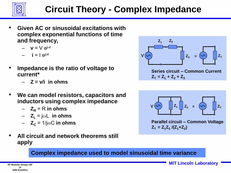
Circuit Theory - Complex Impedance
• Given AC or sinusoidal excitations with complex exponential functions of time and frequency,
– v = V ej t
– i = I ej t
• Impedance is the ratio of voltage to current*
– Z = v/i in ohms
• We can model resistors, capacitors and inductors using complex impedance
– ZR = R in ohms
– ZL = j L in ohms
– ZC = 1/j C in ohms
• All circuit and network theorems still apply
ZT
Parallel circuit – Common Voltage
ZT = Z1Z2 /(Z1+Z2)
Z2Z1
Z3
Z2Z1
ZT
Series circuit – Common Current
ZT = Z1 + Z2 + Z3
v =
=v
Complex impedance used to model sinusoidal time variance
MIT Lincoln LaboratoryRF Modular Design IAP
15
JHW 5/12/2011
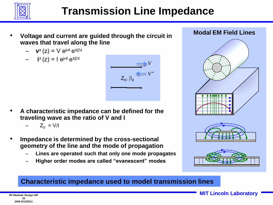
Modal EM Field Lines
Transmission Line Impedance
• Voltage and current are guided through the circuit in waves that travel along the line
– v± (z) = V ej t e±j z
– i± (z) = I ej t e±j z
• A characteristic impedance can be defined for the traveling wave as the ratio of V and I
– Z0 = V/I
• Impedance is determined by the cross-sectional geometry of the line and the mode of propagation
– Lines are operated such that only one mode propagates
– Higher order modes are called “evanescent” modes
Characteristic impedance used to model transmission lines
VZ0,
V
MIT Lincoln LaboratoryRF Modular Design IAP
16
JHW 5/12/2011
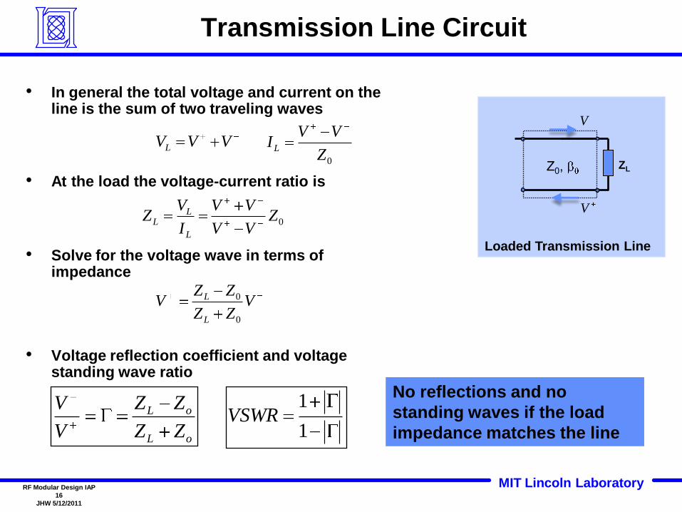
Transmission Line Circuit
• In general the total voltage and current on the line is the sum of two traveling waves
• At the load the voltage-current ratio is
• Solve for the voltage wave in terms of impedance
• Voltage reflection coefficient and voltage standing wave ratio
VVVL
0ZVV
VV
I
VZ
L
LL
VZZ
ZZV
L
L
0
0
Loaded Transmission Line
ZL
V
Z0,
V
oL
oL
ZZ
ZZ
V
V
0Z
VVIL
No reflections and no
standing waves if the load
impedance matches the line1
1VSWR

MIT Lincoln LaboratoryRF Modular Design IAP
18
JHW 5/12/2011
Microwave Networks - History
• The MIT Radiation Laboratory developed RADAR technology for the war effort from 1940-1945
• MIT Rad. Lab. 28 Volume Series
“Authors were selected to remain at work at MIT for six months or more after the work of the Radiation Laboratory was complete. These volumes stand as a monument to this group…. and a memorial to the unnamed thousands of other scientists, engineers, and others ….” – L.A. DuBridge, Lab Director
Center and right images © McGraw Hill. All rights reserved. This content is excluded fromour Creative Commons license. For more information, see http://ocw.mit.edu/fairuse.
MIT Lincoln LaboratoryRF Modular Design IAP
19
JHW 5/12/2011
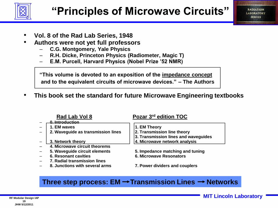
“Principles of Microwave Circuits”
• Vol. 8 of the Rad Lab Series, 1948• Authors were not yet full professors
– C.G. Montgomery, Yale Physics– R.H. Dicke, Princeton Physics (Radiometer, Magic T)– E.M. Purcell, Harvard Physics (Nobel Prize ’52 NMR)
“This volume is devoted to an exposition of the impedance concept
and to the equivalent circuits of microwave devices.” – The Authors
• This book set the standard for future Microwave Engineering textbooks
Rad Lab Vol 8 Pozar 3rd edition TOC– 0. Introduction– 1. EM waves 1. EM Theory– 2. Waveguide as transmission lines 2. Transmission line theory
3. Transmission lines and waveguides– 3. Network theory 4. Microwave network analysis– 4. Microwave circuit theorems– 5. Waveguide circuit elements 5. Impedance matching and tuning– 6. Resonant cavities 6. Microwave Resonators– 7. Radial transmission lines– 8. Junctions with several arms 7. Power dividers and couplers
Three step process: EM Transmission Lines Networks
MIT Lincoln LaboratoryRF Modular Design IAP
20
JHW 5/12/2011
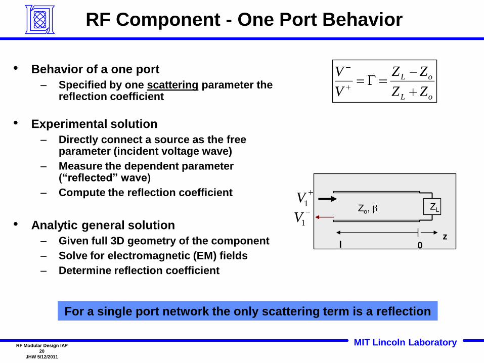
RF Component - One Port Behavior
z
ZL
l
Zo,
0
For a single port network the only scattering term is a reflection
1V
1V
• Behavior of a one port
– Specified by one scattering parameter the reflection coefficient
• Experimental solution
– Directly connect a source as the free parameter (incident voltage wave)
– Measure the dependent parameter (“reflected” wave)
– Compute the reflection coefficient
• Analytic general solution
– Given full 3D geometry of the component
– Solve for electromagnetic (EM) fields
– Determine reflection coefficient
oL
oL
ZZ
ZZ
V
V

MIT Lincoln LaboratoryRF Modular Design IAP
21
JHW 5/12/2011
Circuit Component Two Port Behavior
• Behavior of a two port
– Specified by four parameters
– Only two are dependent parameters
• Experimental general solution
– Remove one of the free parameters (open circuit or short circuit condition)
– Directly connect a voltage or current source as the free parameter
– Measure the two dependent parameters
– Repeat to determine current-voltage relationship at both ports
• Analytic general solution
– Given full 3D geometry of the component
– Solve for electromagnetic (EM) fields
– Determine current-voltage relationship at the ports
Two Port Network Model
1v1i
2v2i
Z
2221
1211
zz
zzZ
02
1
221
1
111
ii
vz
i
vz
01
2
112
2
222
ii
vz
i
vz
Z1v Z 2v
MIT Lincoln LaboratoryRF Modular Design IAP
22
JHW 5/12/2011
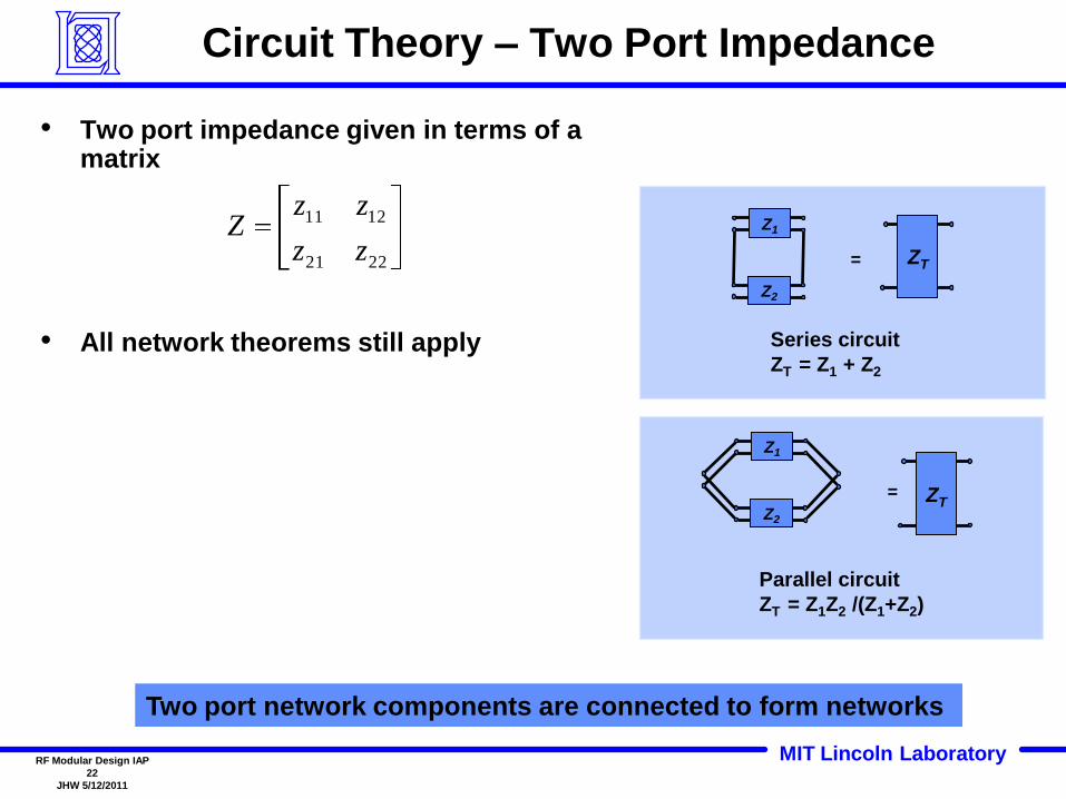
Circuit Theory – Two Port Impedance
• Two port impedance given in terms of a matrix
• All network theorems still apply
Parallel circuit
ZT = Z1Z2 /(Z1+Z2)
Series circuit
ZT = Z1 + Z2
=
=
Two port network components are connected to form networks
ZT
Z1
Z2
ZT
Z1
Z2
2221
1211
zz
zzZ
MIT Lincoln LaboratoryRF Modular Design IAP
23
JHW 5/12/2011
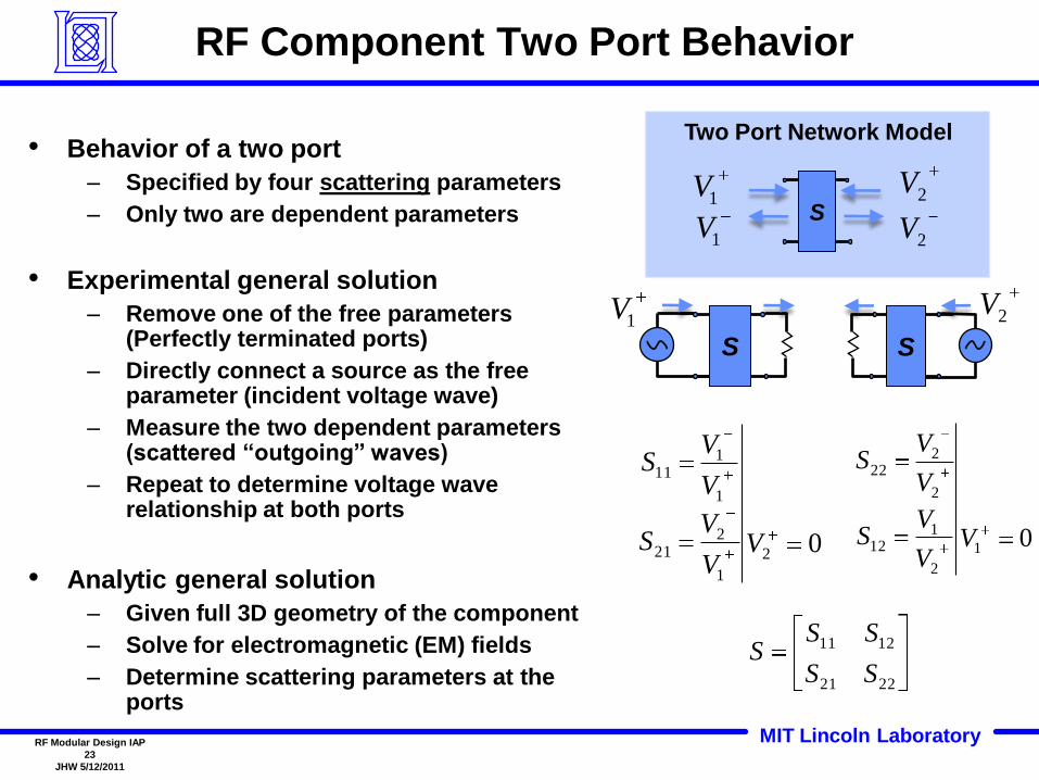
RF Component Two Port Behavior
• Behavior of a two port
– Specified by four scattering parameters
– Only two are dependent parameters
• Experimental general solution
– Remove one of the free parameters (Perfectly terminated ports)
– Directly connect a source as the free parameter (incident voltage wave)
– Measure the two dependent parameters (scattered “outgoing” waves)
– Repeat to determine voltage wave relationship at both ports
• Analytic general solution
– Given full 3D geometry of the component
– Solve for electromagnetic (EM) fields
– Determine scattering parameters at the ports
Two Port Network Model
S
S S
1V
1V
2V
2V
2221
1211
SS
SSS
02
1
221
1
111
VV
VS
V
VS
01
2
112
2
222
VV
VS
V
VS
1V 2V
MIT Lincoln LaboratoryRF Modular Design IAP
24
JHW 5/12/2011
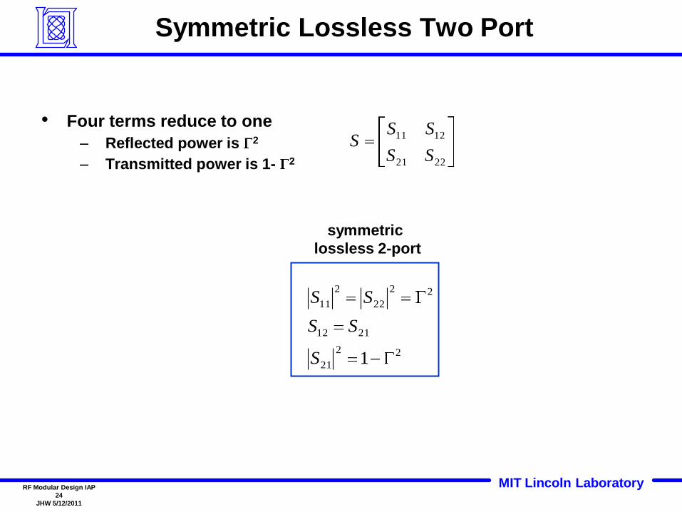
Symmetric Lossless Two Port
• Four terms reduce to one
– Reflected power is 2
– Transmitted power is 1- 2 2221
1211
SS
SSS
22
21
2112
22
22
2
11
1S
SS
SS
symmetric
lossless 2-port
MIT Lincoln LaboratoryRF Modular Design IAP
25
JHW 5/12/2011
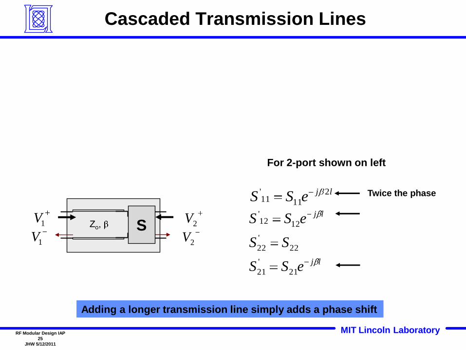
Cascaded Transmission Lines
lj
lj
eSS
SS
eSS
21
'
21
22
'
22
1212'
ljeSS 2
1111'
1V
1V2V
2VS
Adding a longer transmission line simply adds a phase shift
Zo,
For 2-port shown on left
Twice the phase
MIT Lincoln LaboratoryRF Modular Design IAP
26
JHW 5/12/2011
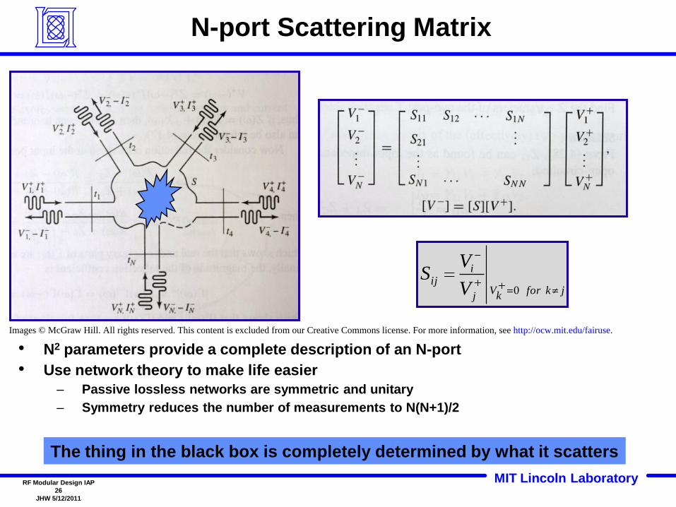
N-port Scattering Matrix
• N2 parameters provide a complete description of an N-port
• Use network theory to make life easier
– Passive lossless networks are symmetric and unitary
– Symmetry reduces the number of measurements to N(N+1)/2
The thing in the black box is completely determined by what it scatters
jkfork
Vj
iij
V
VS
0
Images © McGraw Hill. All rights reserved. This content is excluded from our Creative Commons license. For more information, see http://ocw.mit.edu/fairuse.
MIT Lincoln LaboratoryRF Modular Design IAP
27
JHW 5/12/2011
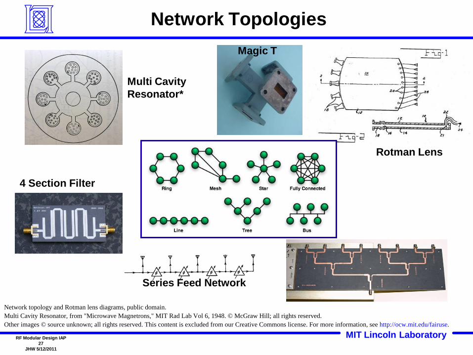
Network Topologies
Rotman Lens
4 Section Filter
Multi Cavity
Resonator*
Magic T
Series Feed Network
Network topology and Rotman lens diagrams, public domain.Multi Cavity Resonator, from "Microwave Magnetrons," MIT Rad Lab Vol 6, 1948. © McGraw Hill; all rights reserved.Other images © source unknown; all rights reserved. This content is excluded from our Creative Commons license. For more information, see http://ocw.mit.edu/fairuse.
MIT Lincoln LaboratoryRF Modular Design IAP
28
JHW 5/12/2011
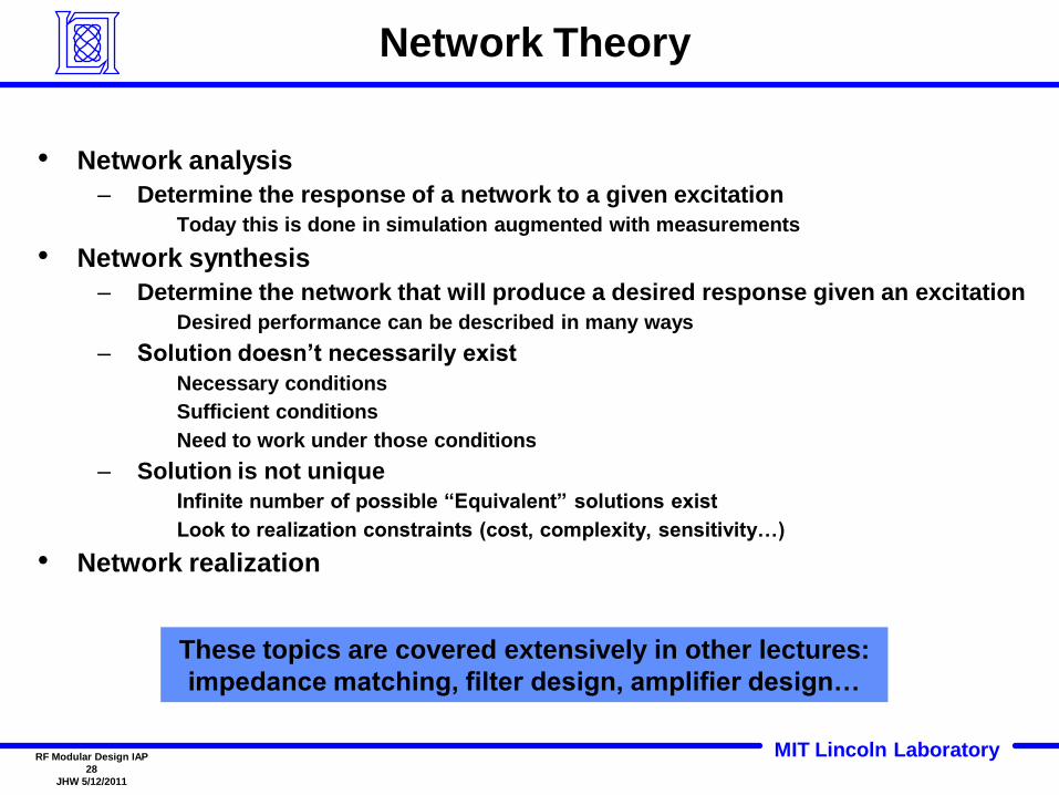
Network Theory
• Network analysis
– Determine the response of a network to a given excitation
Today this is done in simulation augmented with measurements
• Network synthesis
– Determine the network that will produce a desired response given an excitation
Desired performance can be described in many ways
– Solution doesn’t necessarily exist
Necessary conditions
Sufficient conditions
Need to work under those conditions
– Solution is not unique
Infinite number of possible “Equivalent” solutions exist
Look to realization constraints (cost, complexity, sensitivity…)
• Network realization
These topics are covered extensively in other lectures:
impedance matching, filter design, amplifier design…

MIT Lincoln LaboratoryRF Modular Design IAP
29
JHW 5/12/2011
• Introduction
• Circuit and Network Theory
• RF Measurements
• RF Design/Build
• Summary
Outline

MIT Lincoln LaboratoryRF Modular Design IAP
30
JHW 5/12/2011
Measuring an RF component
Specific S parameters are summarized in spec sheets, with full parameters given as electronic files, or you can measure them
Results
CAD model of evaluation board
SZo, Zo,

MIT Lincoln LaboratoryRF Modular Design IAP
31
JHW 5/12/2011
Vector Network Analyzer
• Corresponds to frequency domain network analysis
• Narrow band signal is swept into the DUT through a calibrated reference plane
• Direct measurement of 2-port S-parameters (Measures S11, S12, S21, and S22)
• Multiport networks are measured two ports at a time terminating all other ports
HP 8542A Automatic Network Analyzer *
* Source: Hewlett Packard Journal, February 1970, page 3.© Hewlett Packard Company. All rights reserved. This content is excluded from our Creative Commons license. For more information, see http://ocw.mit.edu/fairuse.** Kristan Tuttle Gr 39
Modern network analyzer measurement**

MIT Lincoln LaboratoryRF Modular Design IAP
32
JHW 5/12/2011
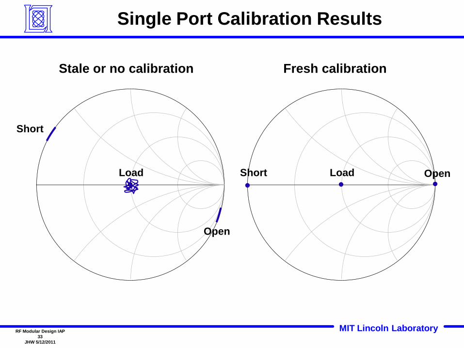
Network Analyzer Calibration
• Purpose of calibration:
– Definition of S-parameters require matched ports
– Remove systematic errors caused by the equipment
– Enhance accuracy, repeatability, stability
• When should you re-calibrate?
– You change settings on the analyzer (frequency band, sweep time…)
– You change the test set-up (move cables, change sex on connectors…)
– Someone else uses the analyzer
• Types of calibration
– Electronic calibration is the standard used today
– Manual calibration takes longer
Single port cal. using calibration kit (2-5 min.)
Full two port cal. (5 - 10 min. sliding load optional)
jkfork
Vj
iij
V
VS
0
MIT Lincoln LaboratoryRF Modular Design IAP
33
JHW 5/12/2011
freq (1.000GHz to 20.00GHz)
Gam
ma
Single Port Calibration Results
freq (1.000GHz to 20.00GHz)
Gam
ma Load
Short
Stale or no calibration Fresh calibration
OpenLoadShort
Open
MIT Lincoln LaboratoryRF Modular Design IAP
34
JHW 5/12/2011
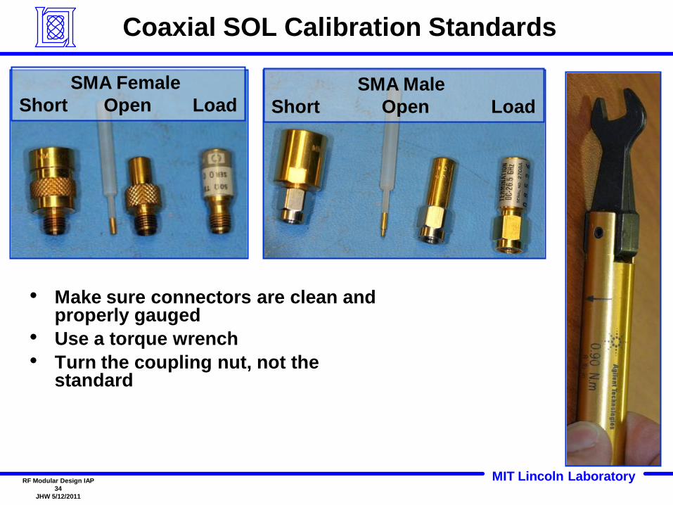
Coaxial SOL Calibration Standards
SMA Female
Short Open LoadSMA Male
Short Open Load
• Make sure connectors are clean and properly gauged
• Use a torque wrench
• Turn the coupling nut, not the standard
MIT Lincoln LaboratoryRF Modular Design IAP
35
JHW 5/12/2011
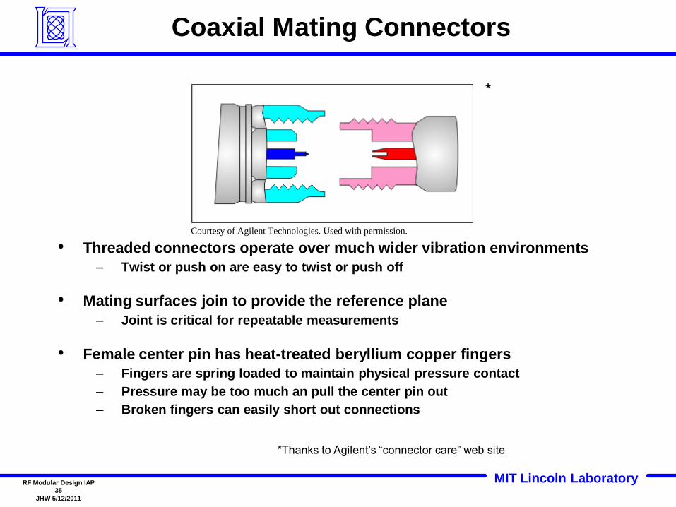
Coaxial Mating Connectors
• Threaded connectors operate over much wider vibration environments
– Twist or push on are easy to twist or push off
• Mating surfaces join to provide the reference plane
– Joint is critical for repeatable measurements
• Female center pin has heat-treated beryllium copper fingers
– Fingers are spring loaded to maintain physical pressure contact
– Pressure may be too much an pull the center pin out
– Broken fingers can easily short out connections
*Thanks to Agilent’s “connector care” web site
*
Courtesy of Agilent Technologies. Used with permission.

MIT Lincoln LaboratoryRF Modular Design IAP
36
JHW 5/12/2011
Waveguide TRL Calibration Standards
Reflect
Line
(short section
of waveguide)
Q 40-50 GHzKa 30 GHzKu 15-20 GHz
Thru measurement is a mating of the two
waveguide reference planes
MIT Lincoln LaboratoryRF Modular Design IAP
37
JHW 5/12/2011
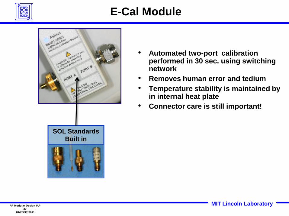
E-Cal Module
• Automated two-port calibration performed in 30 sec. using switching network
• Removes human error and tedium
• Temperature stability is maintained by in internal heat plate
• Connector care is still important!
SOL Standards
Built in
MIT Lincoln LaboratoryRF Modular Design IAP
38
JHW 5/12/2011
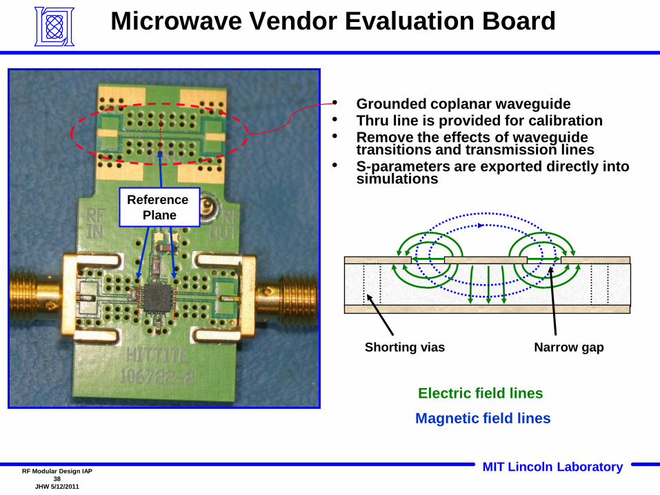
Microwave Vendor Evaluation Board
• Grounded coplanar waveguide • Thru line is provided for calibration• Remove the effects of waveguide
transitions and transmission lines• S-parameters are exported directly into
simulations
Electric field lines
Magnetic field lines
Narrow gapShorting vias
Reference
Plane

MIT Lincoln LaboratoryRF Modular Design IAP
39
JHW 5/12/2011
• Introduction
• Circuit and Network Theory
• RF Measurements
• RF Design/Build
• Summary
Outline
MIT Lincoln LaboratoryRF Modular Design IAP
40
JHW 5/12/2011
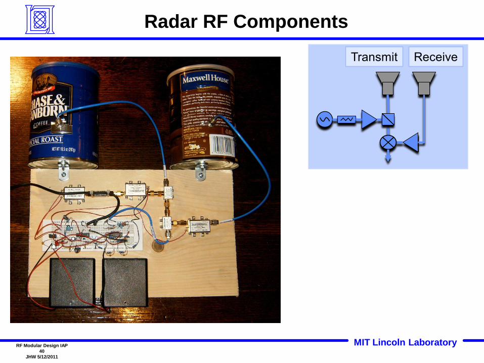
Radar RF Components
Transmit Receive

MIT Lincoln LaboratoryRF Modular Design IAP
41
JHW 5/12/2011
Radar RF Components
Transmit Receive

MIT Lincoln LaboratoryRF Modular Design IAP
42
JHW 5/12/2011
Transmit Chain
ReceiveTransmit
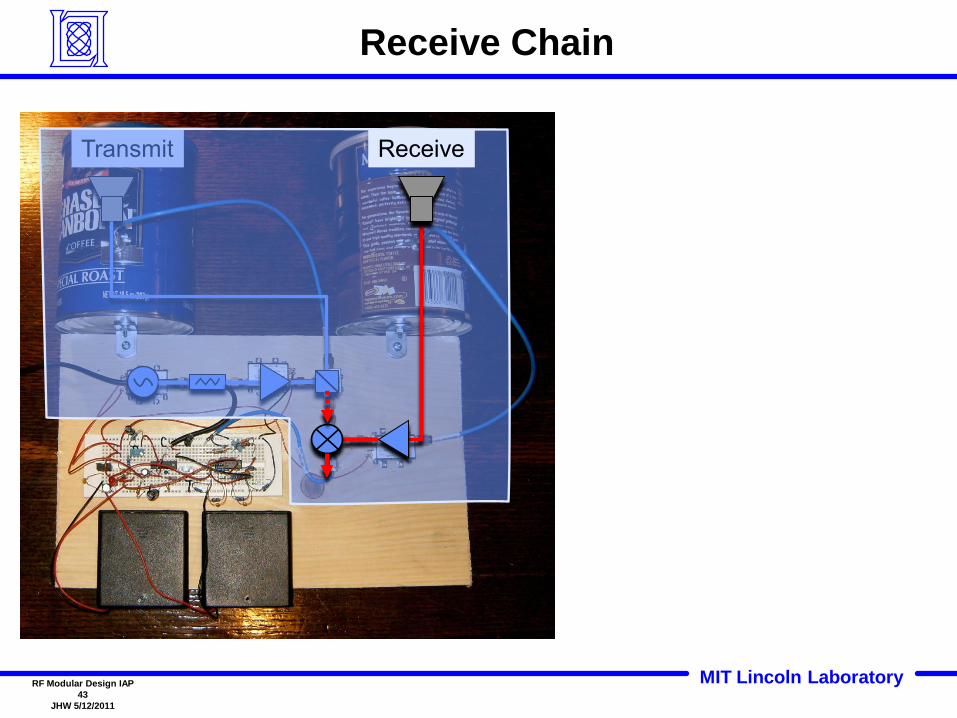
MIT Lincoln LaboratoryRF Modular Design IAP
43
JHW 5/12/2011
Transmit
Receive Chain
Receive
MIT Lincoln LaboratoryRF Modular Design IAP
44
JHW 5/12/2011
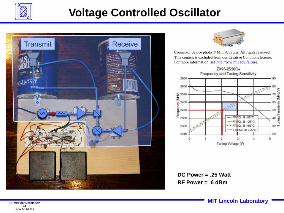
Voltage Controlled Oscillator
Transmit Receive
DC Power = .25 Watt
RF Power = 6 dBm
Connector device photo © Mini-Circuits. All rights reserved.This content is excluded from our Creative Commons license.For more information, see http://ocw.mit.edu/fairuse.

MIT Lincoln LaboratoryRF Modular Design IAP
45
JHW 5/12/2011
Attenuator
Transmit Receive
DC Power = .25 Watt
RF Power = 6 – 3.3 = 2.7 dBm
Connector device photo © Mini-Circuits. All rights reserved.This content is excluded from our Creative Commons license.For more information, see http://ocw.mit.edu/fairuse.

MIT Lincoln LaboratoryRF Modular Design IAP
46
JHW 5/12/2011
Transmit Receive
Amplifier
DC Power = .25 + .4 = .65 Watt
RF Power = 2.7 + 14 = 16.7 dBm
Connector device photo © Mini-Circuits. All rights reserved.This contentis excluded from our Creative Commons license. For more information,see http://ocw.mit.edu/fairuse.
MIT Lincoln LaboratoryRF Modular Design IAP
47
JHW 5/12/2011
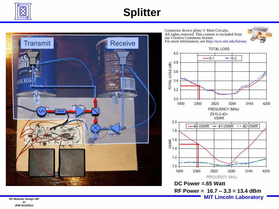
Transmit Receive
Splitter
DC Power =.65 Watt
RF Power = 16.7 – 3.3 = 13.4 dBm
Connector device photo © Mini-Circuits.All rights reserved. This content is excluded fromour Creative Commons license.For more information, see http://ocw.mit.edu/fairuse.

MIT Lincoln LaboratoryRF Modular Design IAP
48
JHW 5/12/2011
Transmit Receive
Antenna
2.45 GHz
DC Power =.65 Watt
RF Power = 13.4 + 11 = 24.4 dBm EIRP

MIT Lincoln LaboratoryRF Modular Design IAP
49
JHW 5/12/2011
Transmit Chain Summary
ReceiveTransmit • DC Power = .65 Watt
• Tx Power = 24 dBm EIRP
• FCC ISM Req. < 1 Watt EIRP
• Provide copy of Tx waveform to receive chain (13dBm)

MIT Lincoln LaboratoryRF Modular Design IAP
50
JHW 5/12/2011
Transmit
Receive Chain
Receive
MIT Lincoln LaboratoryRF Modular Design IAP
51
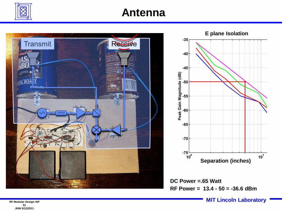
JHW 5/12/2011
Transmit
Antenna
Receive
DC Power =.65 Watt
RF Power = 13.4 - 50 = -36.6 dBm
E plane Isolation
Separation (inches)
MIT Lincoln LaboratoryRF Modular Design IAP
52
JHW 5/12/2011
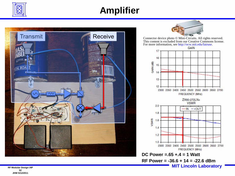
Amplifier
Transmit Receive
DC Power =.65 +.4 = 1 Watt
RF Power = -36.6 + 14 = -22.6 dBm
Connector device photo © Mini-Circuits. All rights reserved.This content is excluded from our Creative Commons license.For more information, see http://ocw.mit.edu/fairuse.
MIT Lincoln LaboratoryRF Modular Design IAP
53
JHW 5/12/2011
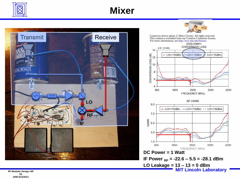
Mixer
Transmit Receive
DC Power = 1 Watt
IF Power RF = -22.6 – 5.5 = -28.1 dBm
LO Leakage = 13 – 13 = 0 dBm
LO
RF
IF
Connector device photo © Mini-Circuits. All rights reserved.This content is excluded from our Creative Commons license.For more information, see http://ocw.mit.edu/fairuse.

MIT Lincoln LaboratoryRF Modular Design IAP
54
JHW 5/12/2011
Transmit
Receive Chain Summary
Receive • DC Power = 1 Watt
• IF Power = -28 dBm
• Mixer uses copy of Txwaveform
MIT Lincoln LaboratoryRF Modular Design IAP
55
JHW 5/12/2011
• Introduction
• Circuit and Network Theory
• RF Measurements
• RF Design/Build
• Summary
Outline
MIT Lincoln LaboratoryRF Modular Design IAP
56
JHW 5/12/2011
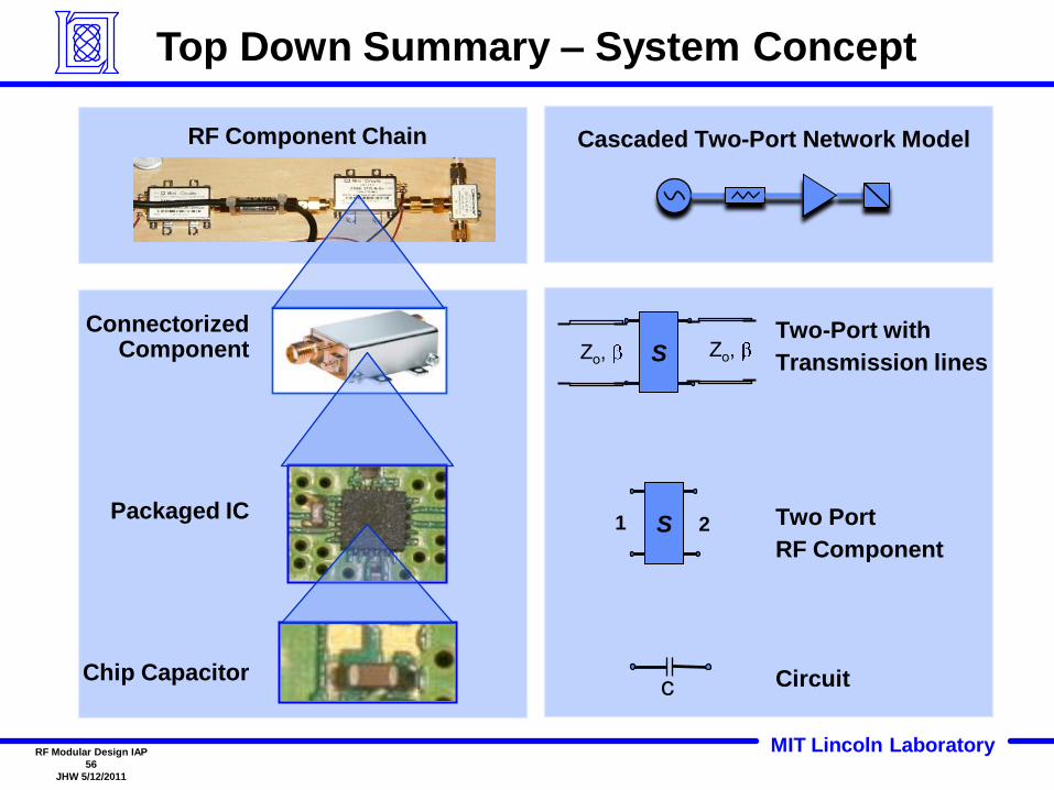
Top Down Summary – System Concept
ConnectorizedComponent
Packaged IC
Chip Capacitor
RF Component Chain Cascaded Two-Port Network Model
Two-Port with
Transmission lines
Two Port
RF Component
Circuit
S1 2
c
SZo, Zo,
MIT Lincoln LaboratoryRF Modular Design IAP
57
JHW 5/12/2011
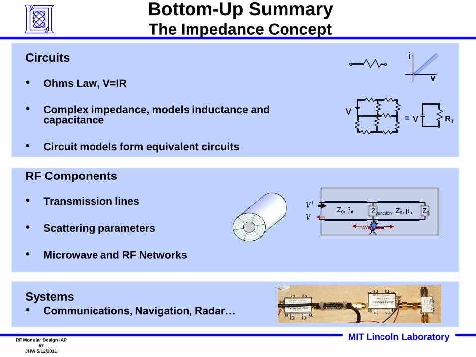
Bottom-Up SummaryThe Impedance Concept
Circuits
• Ohms Law, V=IR
• Complex impedance, models inductance and capacitance
• Circuit models form equivalent circuits
RF Components
• Transmission lines
• Scattering parameters
• Microwave and RF Networks
Systems• Communications, Navigation, Radar…
ZJunctionZ0, Z0Z0, V
V
v
i
vRT
= v

MIT OpenCourseWare http://ocw.mit.edu
Resource: Build a Small Radar System Capable of Sensing Range, Doppler, and Synthetic Aperture Radar Imaging Dr. Gregory L. Charvat, Mr. Jonathan H. Williams, Dr. Alan J. Fenn, Dr. Steve Kogon, Dr. Jeffrey S. Herd
The following may not correspond to a particular course on MIT OpenCourseWare, but has been provided by the author as an individual learning resource.
For information about citing these materials or our Terms of Use, visit: http://ocw.mit.edu/terms.


