Modified Booth Encoding Radix-4 8-bit...
20
Modified Booth Encoding Radix-4 8-bit Multiplier Final Project Report Da Huang, Afsaneh Nassery
Transcript of Modified Booth Encoding Radix-4 8-bit...
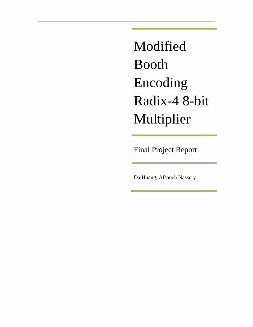
Modified Booth Encoding Radix-4 8-bit Multiplier
Final Project Report
Da Huang, Afsaneh Nassery
Page 2 of 20
Table of Contents
Table of Contents ...................................................................................................................... 2 Abstract: .................................................................................................................................... 3
System Diagram: ............................................................................................................... 3 Performance Estimation: ................................................................................................... 5
Transistor number and Area estimation .................................................................... 5 Time Delay: ............................................................................................................... 6 Power Consumption: ................................................................................................. 6
Project Floor plane: ........................................................................................................... 7 Sub circuit Design ..................................................................................................................... 8
Encoder Circuit ............................................................... Error! Bookmark not defined. Decoder Circuit ............................................................... Error! Bookmark not defined. 12 Bit Adder circuit ......................................................................................................... 12
Full System Design ................................................................................................................. 13 Test simulations………………………………………………………………………… 16
Summary ................................................................................. Error! Bookmark not defined. Reference ................................................................................................................................ 20
Page 3 of 20
Abstract:
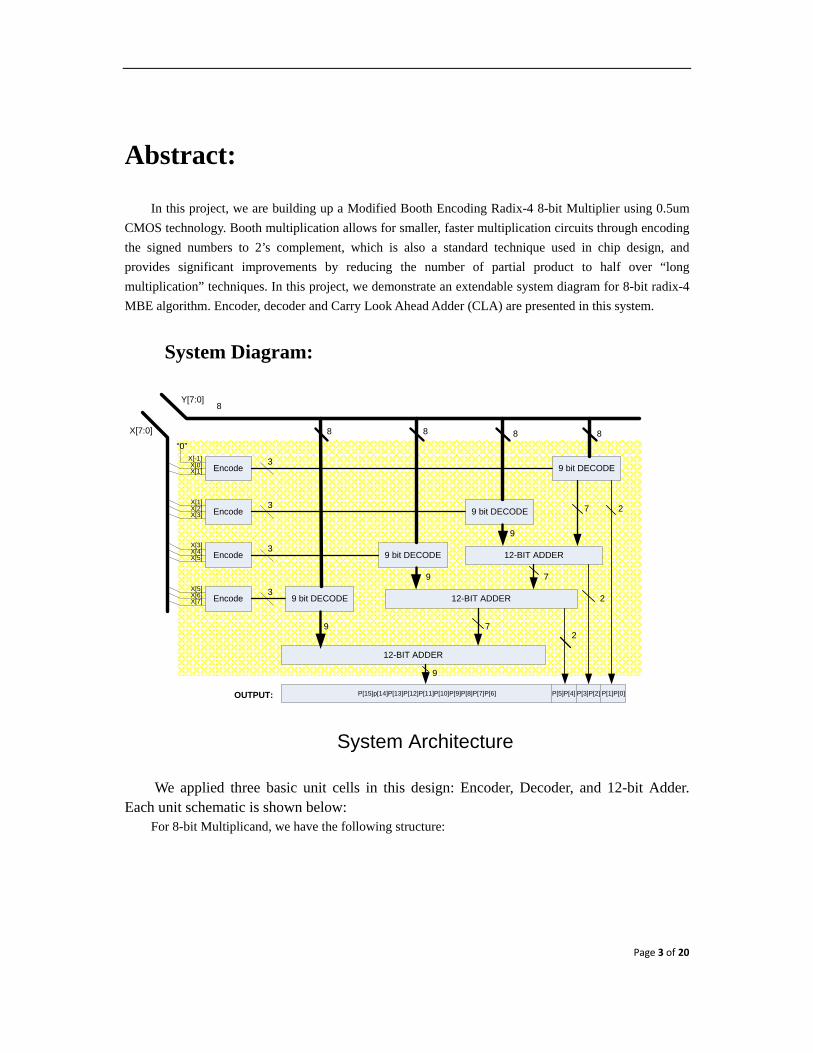
In this project, we are building up a Modified Booth Encoding Radix-4 8-bit Multiplier using 0.5um CMOS technology. Booth multiplication allows for smaller, faster multiplication circuits through encoding the signed numbers to 2’s complement, which is also a standard technique used in chip design, and provides significant improvements by reducing the number of partial product to half over “long multiplication” techniques. In this project, we demonstrate an extendable system diagram for 8-bit radix-4 MBE algorithm. Encoder, decoder and Carry Look Ahead Adder (CLA) are presented in this system.
System Diagram:
Encode
Encode
Encode
Encode
X[7:0]
“0”
X[0]X[1]
X[-1]
X[2]X[3]
X[1]
X[4]X[5]
X[3]
X[6]X[7]
X[5]
Y[7:0]
9 bit DECODE
9 bit DECODE
9 bit DECODE
9 bit DECODE
12-BIT ADDER
12-BIT ADDER
12-BIT ADDER
P[1]P[0]P[3]P[2]P[5]P[4]P[15]p[14]P[13]P[12]P[11]P[10]P[9]P[8]P[7]P[6]OUTPUT:
System Architecture
8
8 8 8 8
3
3
3
3
2
2
2
7
7
7
9
9
9
9
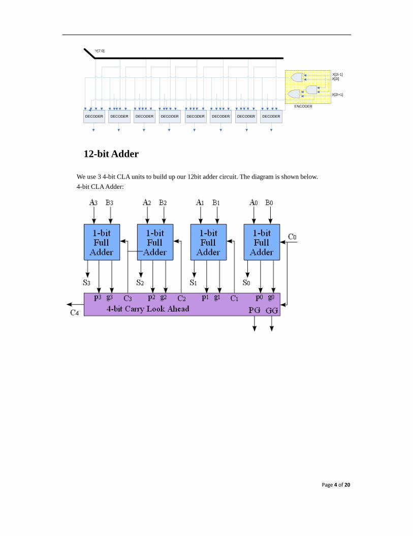
We applied three basic unit cells in this design: Encoder, Decoder, and 12-bit Adder. Each unit schematic is shown below:
For 8-bit Multiplicand, we have the following structure:
Page 4 of 20
X[2i-1]X[2i]
X[2i+1]
ENCODER
DECODERDECODERDECODERDECODERDECODERDECODERDECODERDECODER
Y[7:0]
12-bit Adder
We use 3 4-bit CLA units to build up our 12bit adder circuit. The diagram is shown below. 4-bit CLA Adder:

Page 5 of 20
Performance Estimation:
Transistor number and Area estimation
T
ype of
Gate
Num of
Transisto
r
Number
needed
Transisto
r Est.
Area for
Gate(um
2)
Area
Est.
And2 6 134 804 595 79730
OR2 6 62 372 577.5 35805
NOR2 4 32 128 315 10080
XNOR
2
8
32 256 1147.5 36720
XOR2 8 30 240 885 26550
OR3 8 18 144 612.5 11025
AND3 8
30 240 707.25
21217.
5
Total
Transist
or
2184 Total
Area
0.265
mm2
Page 6 of 20
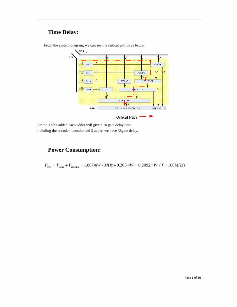
Time Delay:
From the system diagram, we can see the critical path is as below:
For the 12-bit adder, each adder will give a 10 gate delay time. Including the encoder, decoder and 3 adder, we have 38gate delay.
Power Consumption:
1.887 / 0.205 0.2092 ( 100 )total static dynamicP P P mW MHz mW mW f MHz= + = + = =
Page 7 of 20
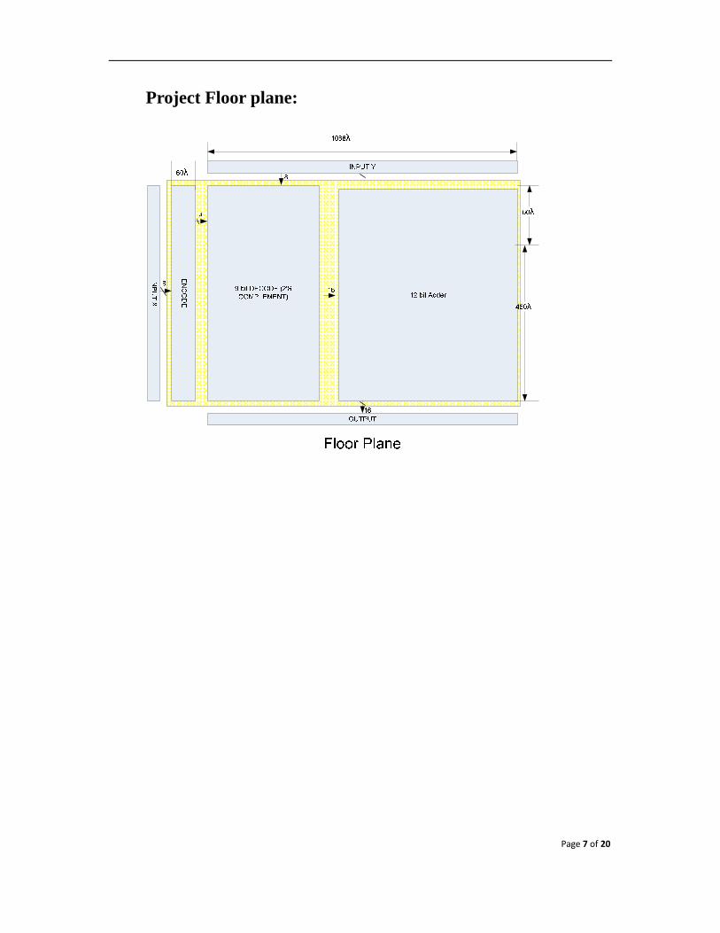
Project Floor plane:
Page 8 of 20
Sub circuit Design
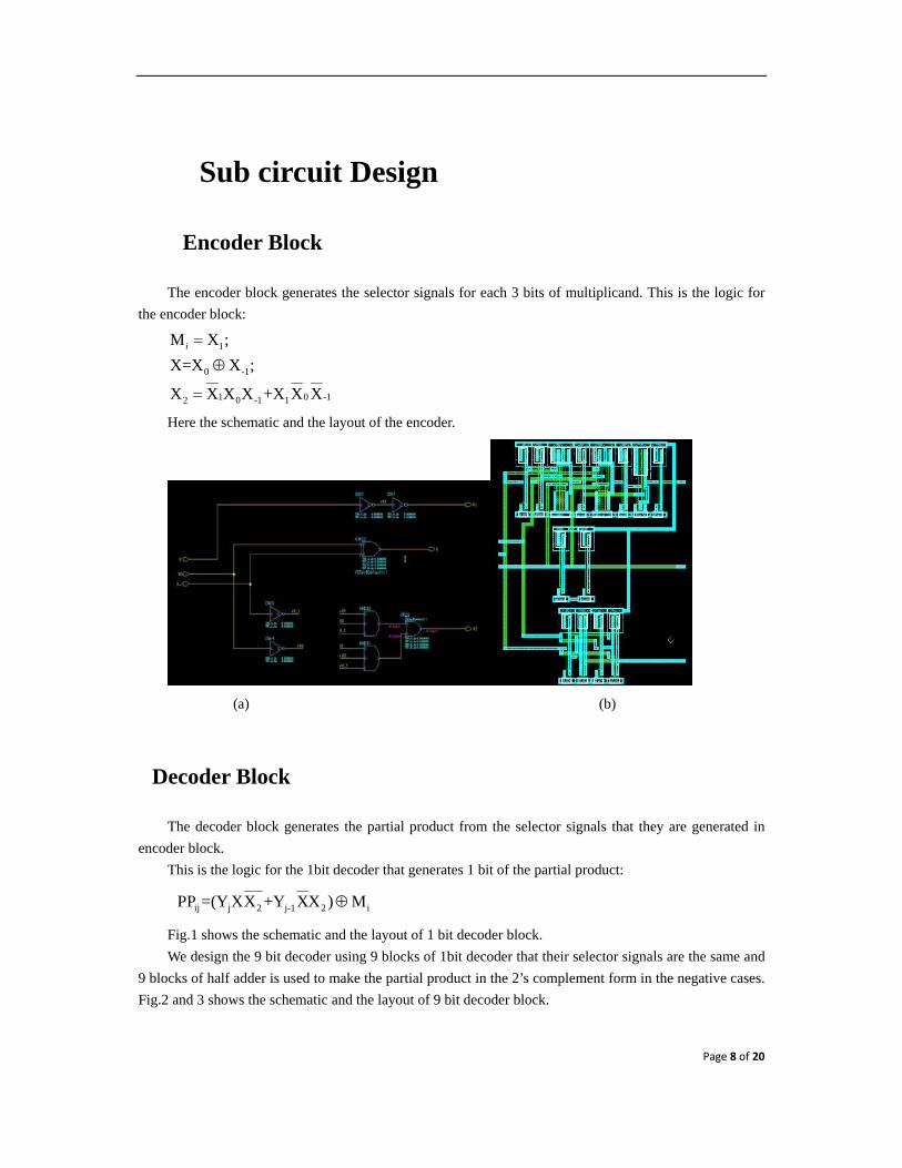
Encoder Block
The encoder block generates the selector signals for each 3 bits of multiplicand. This is the logic for the encoder block:
1
0 -1
1 0 -12 0 -1 1
M X ;X=X X ;
X X X X +X X X
i =
⊕
=
Here the schematic and the layout of the encoder.
(a) (b)
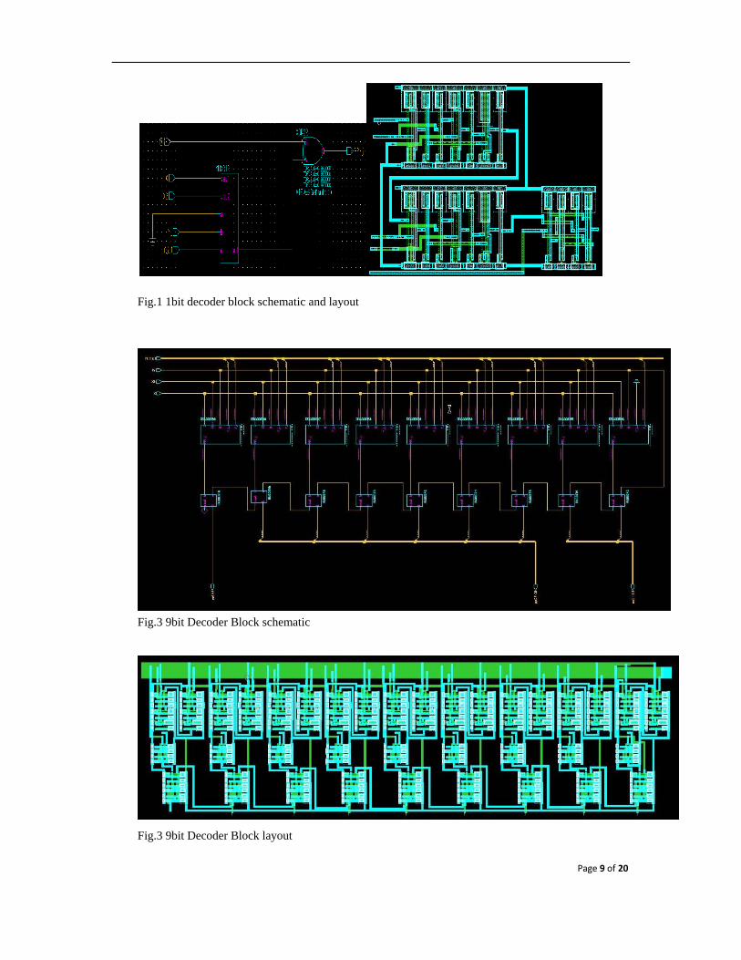
Decoder Block
The decoder block generates the partial product from the selector signals that they are generated in encoder block.
This is the logic for the 1bit decoder that generates 1 bit of the partial product:
ij j 2 j-1 2 iPP =(Y XX +Y XX ) M⊕
Fig.1 shows the schematic and the layout of 1 bit decoder block. We design the 9 bit decoder using 9 blocks of 1bit decoder that their selector signals are the same and
9 blocks of half adder is used to make the partial product in the 2’s complement form in the negative cases. Fig.2 and 3 shows the schematic and the layout of 9 bit decoder block.
Page 9 of 20
Fig.1 1bit decoder block schematic and layout
Fig.3 9bit Decoder Block schematic
Fig.3 9bit Decoder Block layout
Page 10 of 20
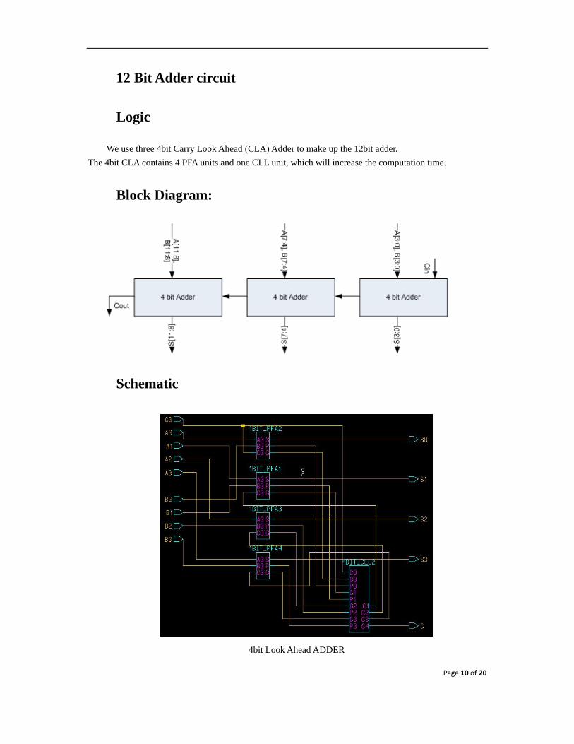
12 Bit Adder circuit
Logic
We use three 4bit Carry Look Ahead (CLA) Adder to make up the 12bit adder. The 4bit CLA contains 4 PFA units and one CLL unit, which will increase the computation time.
Block Diagram:
Schematic
4bit Look Ahead ADDER
Page 11 of 20
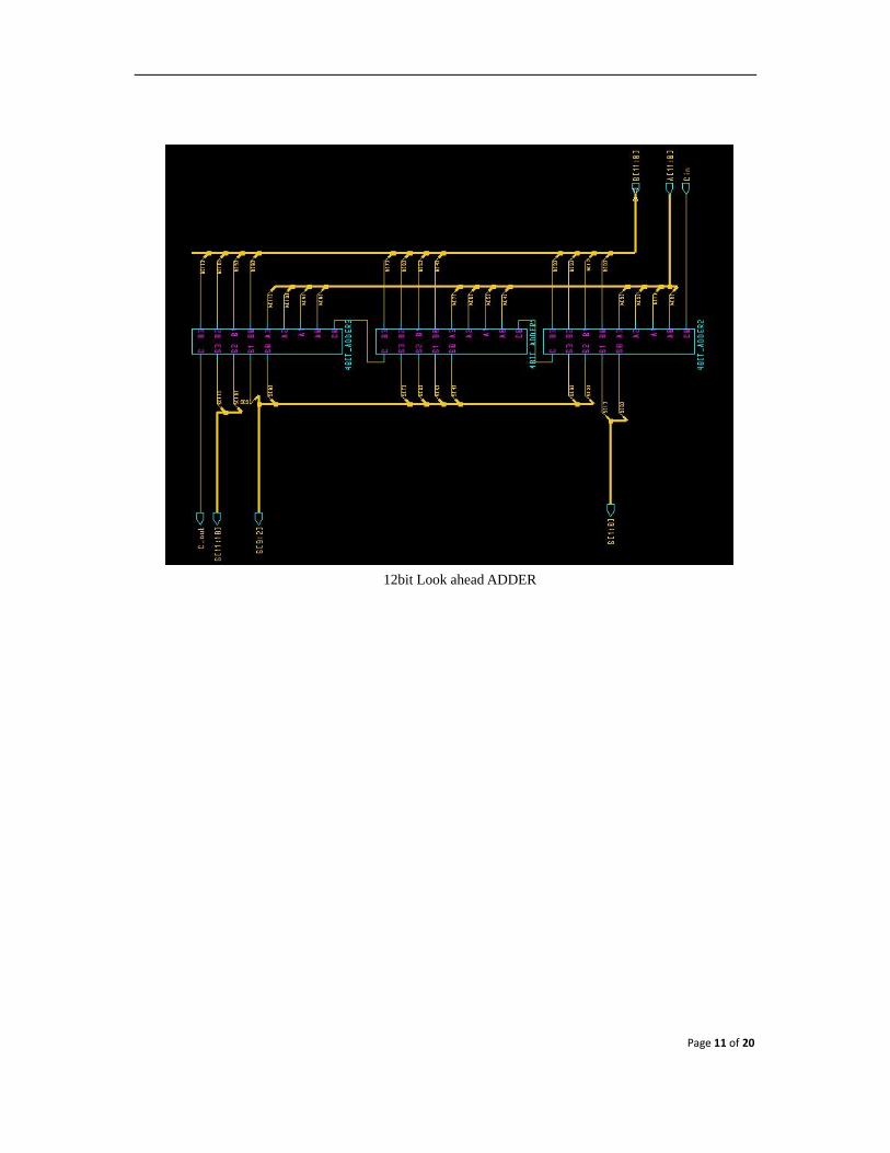
12bit Look ahead ADDER
Page 12 of 20
Layout
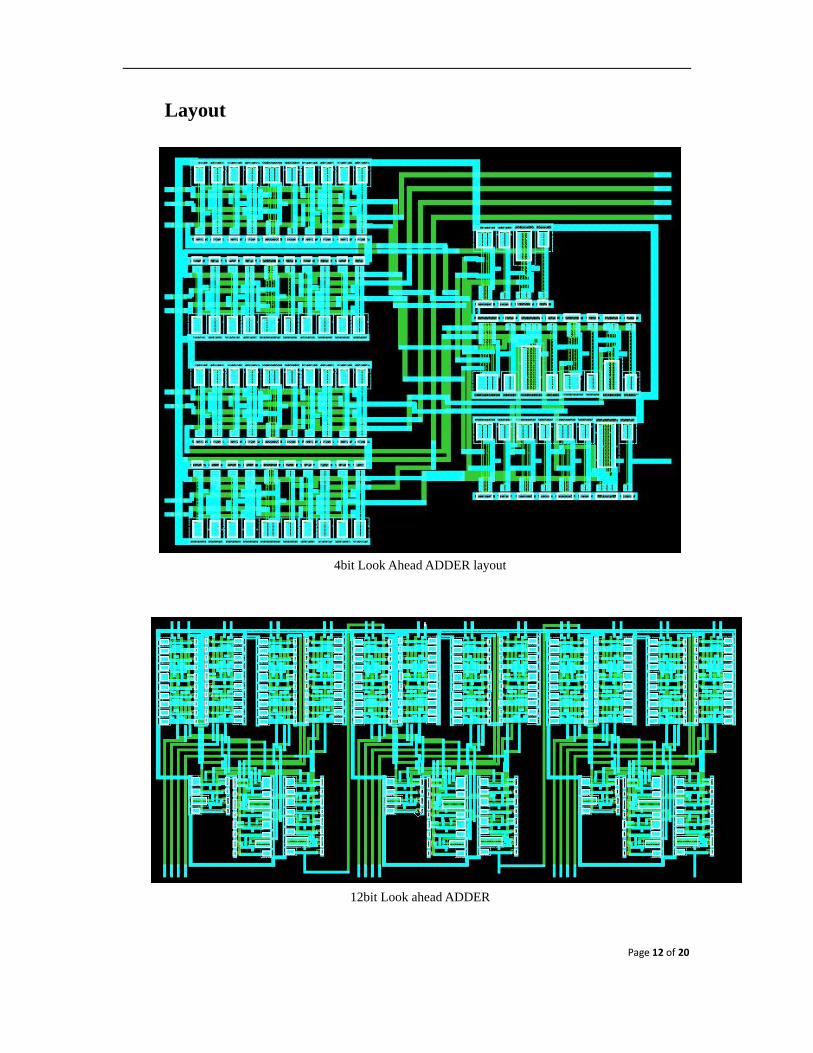
4bit Look Ahead ADDER layout
12bit Look ahead ADDER
Page 13 of 20
Full System Design
Logic
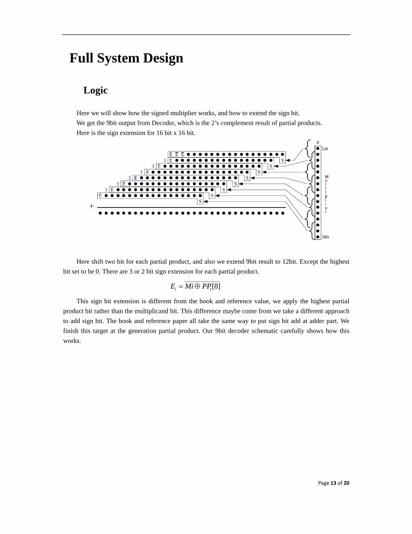
Here we will show how the signed multiplier works, and how to extend the sign bit. We get the 9bit output from Decoder, which is the 2’s complement result of partial products. Here is the sign extension for 16 bit x 16 bit.
Here shift two bit for each partial product, and also we extend 9bit result to 12bit. Except the highest
bit set to be 0. There are 3 or 2 bit sign extension for each partial product.
[8]i iE Mi PP= ⊕
This sign bit extension is different from the book and reference value, we apply the highest partial product bit rather than the multiplicand bit. This difference maybe come from we take a different approach to add sign bit. The book and reference paper all take the same way to put sign bit add at adder part. We finish this target at the generation partial product. Our 9bit decoder schematic carefully shows how this works.
Page 14 of 20
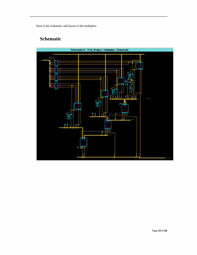
Here is the schematic and layout of the multiplier:
Schematic
Page 15 of 20
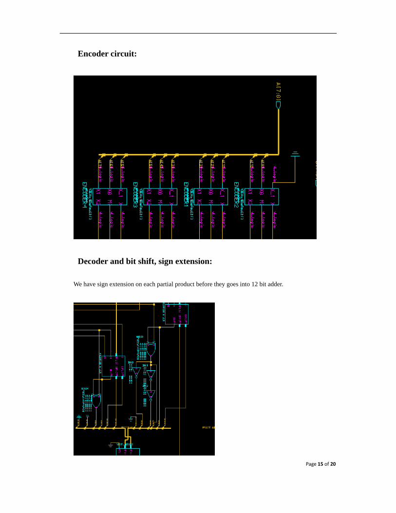
Encoder circuit:
Decoder and bit shift, sign extension:
We have sign extension on each partial product before they goes into 12 bit adder.
Page 16 of 20
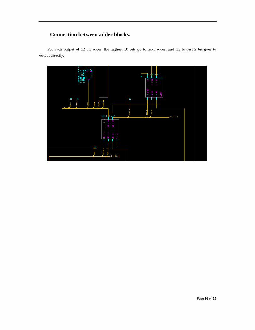
Connection between adder blocks.
For each output of 12 bit adder, the highest 10 bits go to next adder, and the lowest 2 bit goes to output directly.
Page 17 of 20
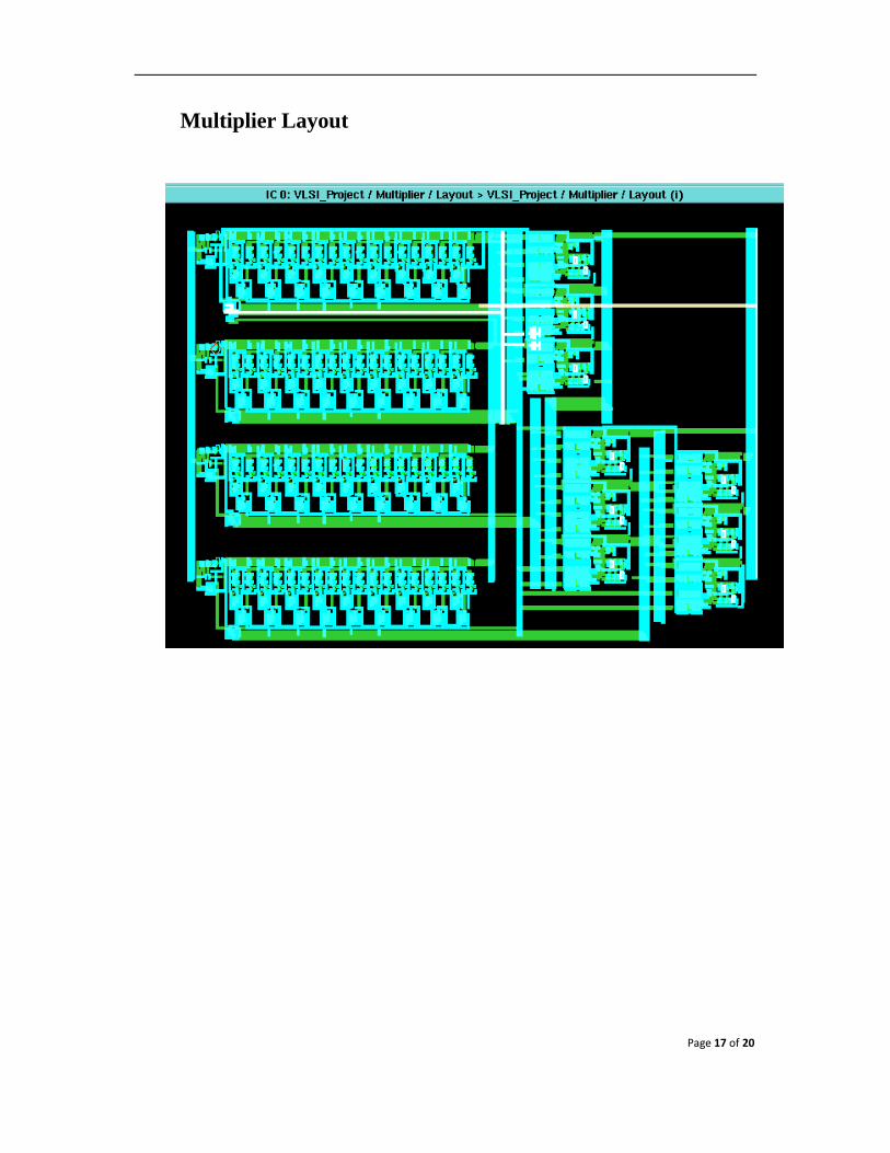
Multiplier Layout
Page 18 of 20
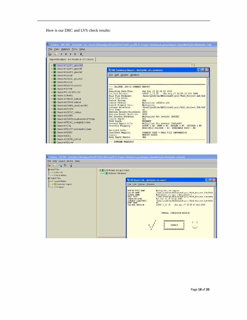
Here is our DRC and LVS check results:

Page 19 of 20
Test Simulations:
Digital Simulation Result:
In order to make sure about the multiplication procedure we wrote the verilog code for all the blocks and check our multiplier with digital simulation. The table shows our simulation result:
A[7:0] B[7:0] Output
00000001 00000001 0000000000000001 00001111 00000010 0000000000011110 00001111 00000100 0000000000111100 00001111 00001111 0000000000110001 10000001 00000100 1111111000000100 10110111 01011010 1110011001010110
Eldo Simulation Result:
12 bit CLA adder Eldo Simulation Result:
Page 20 of 20
Reference
[1]: CMOS VLSI Design: A Circuits and Systems Perspective, Thrid Edition, Neil H.E. Weste, David Harris [2]:G. Bewick, Fast Multiplication: Algorithm and Implementation PhD. Thesis, Stanford University, 1994; [3]: Leonardo L.de Oliveira, Eduardo. C. Sergio B. Array Hybrid Multiplier versus Modified Booth Multiplier: Comparing Area and Power Consumption of Layout Implementations of Signed Radix-4 Architectures. [5]: Vojin G. Oklobdziji. High-Speed VLSI Arithmetic Units: Adders and Multipliers [4 ]:Hsin-Lei Lin, Robert C. Chang, Ming-Tsai Chan. Design of a Novel Radix-4 Booth Multiplier