
Modern Printed Circuits: June, 2014
25
JUNE ‘14 Interview with Zulki Khan President & Founder of Nexlogic PCB DESIGN & ASSEMBLY for High Stakes Medical Electronics New iDesign Fuse Selector Price Quoting for Printed Circuits
-
Upload
eeweb-magazines -
Category
Documents
-
view
217 -
download
1
description
PCB Design & Assembly for High Stakes Medical Electronics - Interview with Zulki Khan, President & Founder of Nexlogic; New iDesign Fuse Selection Tool; Price Quoting for PCBs
Transcript of Modern Printed Circuits: June, 2014
JUNE ‘14
Interview with
Zulki Khan President & Founder of Nexlogic
PCB DESIGN & ASSEMBLY for High Stakes Medical Electronics
New iDesign Fuse Selector
Price Quoting for Printed Circuits

eeweb.com/register
Join Today
READY TO LAUNCH
For the launch of the Tiva C Series Connected LaunchPad, TI has partnered with Exosite, mentioned briefly above, to provide easy access to the LaunchPad from the Internet. The LaunchPad takes about 10 minutes to set up and you can immediately interact with it across the Internet and do things like turn an LED on and off remotely from the website and see the reported temperature as well. It can also display approximate geographic location based on the assigned IP address and display a map of all other connected LaunchPad owners if they are active and plugged-in to Exosite. “In addition, it supports a basic game by enabling someone to interface to the Connected LaunchPad through a serial port from a terminal while someone else is playing with them through their browser. It is basically showing how you can interact remotely with this product and a user even if you are across the globe,” Folkens explained.
START DEVELOPING
The Tiva C Series Connected LaunchPad is shipping now and the price is right; at $19.99 USD, it is less than half the price of other Ethernet-ready kits. The LaunchPad comes complete with quick start and user guides, and ample online support to ensure developers of all backgrounds are well equipped to begin creating cloud-based applications. “We have assembled an online support team to monitor the Engineering-to-Engineering (or E2E) Community,” Folkens said. “Along with this, you also got a free Code Composer Studio Integrated Development Environment, which allows developers to use the full capability. We also support other tool chains like Keil, IAR and Mentor Embedded.
Affordable, versatile, and easy to use, the Tiva Series Connected LaunchPad is well suited for a broad audience and promises to facilitate the expansion of ingenious IoT applications in the cloud. As Folkens concluded, “The target audiences actually are the hobbyists, students and professional engineers. A better way of looking at it is that we are targeting people with innovative ideas and trying to help them get those ideas launched into the cloud.”

Modern Printed Circuits CONTENTS
4
3
PCB is being reflowed or wave soldered, the contamination can outgas and destroy the via and thus the board. When you tent a via, make certain you only do it on one side. An encroached via eliminates this issue by keeping the hole itself open and also has the added benefit versus a tented via of being possible no matter the via size. While tented vias need to be small enough for the solder mask to bridge the drill hole, the encroached via only covers the annular ring and can be as big or small as needed.
Filled vias are also an option, which increase strength, electrical/thermal conductivity, and protect the via from solderwicking and contamination. The main drawback to filled vias is that they can add significant costs to the board. The other methods should have no impact on cost whatsoever.
Every design has different requirements and constraints. However, when possible, utilize these tips by using the largest vias, the appropriate aspect ratio, and by thoughtfully choosing the solder masking style that suits your needs. This will help reduce the overall lifetime costs by increasing reliability of your products.
Solder Dam
Encroached Via
Tented Via
"An encroached via eliminates this issue by keeping the hole itself open and also has the added benefit versus a tented via of being possible no matter the via size."
Content provided courtesy of Advanced Assembly, leader in quick-turn, PCB assembly.For more information on the company, visit www.aa-pcbassembly.com or call 1-800-838-5650.
Our last post covered many of the cost factors used by a fabricator to calculate cost of a printed circuit board. For those with industry experience many of these factors may be obvious but there are other factors that contribute to cost that may be less obvious and we’ll cover several of these today. Having an understanding of these cost factors will not only empower buyers to ask the right questions of their fabricator but will also enable designers to design with optimal performance and cost efficiency.
KEY COST DRIVING FACTORSWhen Quoting Printed Circuit Boards[Part 2] By Peter Brissette, Bay Area Circuits
TOOLING AND TEST CHARGES Tooling costs may include cost for CAM time, film costs, etc. There are a variety of tests that can be performed related to manufacturing a PCB. An Electrical Test would be the most common, which will do a basic open and shorts test of the PCB to make sure it is electrically sound. Additional tests that typically add more costs would be TDR for Impedance Testing, Ionic Testing, etc. The specific costs related to these items vary greatly by manufacturer. FINISH TYPE
The most common finish type is still a lead finish referred to as HASL (Hot Air Solder Leveled). Other finishes can add 10% to 20% or more to the cost. Those include a variety of gold finish options (ENIG, body gold, gold fingers etc.), silver finish options and more. DRILL TYPE We mentioned the mechanical drill cost already in this article. If you need much smaller holes, referred to often as microvias, then a laser drill process is required. Laser drill can add significant costs to the overall process. Another factor would be blind or buried vias. These are vias that do not go all the way through the entire board. Each additional drill process can add as much as 20% or more to the cost. LAMINATION PROCESS Processing a multi-layer printed circuit board that requires something outside the standard process can add costs. Some other processes could be sequential lamination or laminating FR4 with a different material type such as polyamide.
Get a FREE Proto Board at http://www.bayareacircuits.com/freepcb
Customers and buyers who are relatively new to the printed circuit board (PCB) industry may be confused as to how a particular project is priced by the fabricator. In this article series, we’ll begin to demystify the factors used by fabricators to calculate price, empowering you to better plan and price your next PCB project.
KEY COST DRIVING FACTORSWhen Quoting Printed Circuit Boards[Part 1] By Peter Brissette, Bay Area Circuits
To read the previous article, click on the image at the right.
SPECIFICATION STANDARDS IPC Class 2 is a common standard for final PCB inspection and quality processes. Class 3 is a step up from Class 2 that requires additional processes such as coupons and cross-sections to be added to the manufacturing process and can see a cost increase of 15% to 20%. VIA FILL Vias on a PCB are usually not filled completely. They will have copper plating and the finish in the holes but they will not be completely filled. You can fill vias with either non-conductive or conductive material. This process will add 10% or more to the cost of the PCB. FABRICATION Additional costs will be incurred when there is additional fabrication that needs to be done to the finished board. These include things like counterbores, countersinks, complex routing, controlled depth drilling etc. These costs vary greatly. These are many of the primary and secondary variables a fabricator uses when preparing a price quotation for a customer. Of course, for a customer, the price of a printed circuit board is not always a measurement of the true costs in the manufacturing process. Delays in delivery by the fabricator or a board failure because of an inferior manufacturing process can cause the real price to be much higher.
So, when quoting your next printed circuit board project, be sure to clearly identify your project requirements, ask the right questions of your fabricator and design for optimal performance and price efficiency.
6
12
20
As far as PCB assembly and manufacturing, where should the emphasis be placed so that OEM medical electronics sub-assemblies achieve the highest reliability possible?
As I alluded to earlier, maintaining high quality manufacturing translates directly into high reliability. Emphasis must be placed on the quality steps that are embedded in the assembly and manufacturing process. You are always checking, evaluating, tweaking, and streamlining that process to make it as strong as possible to achieve the reliability medical electronics OEMs demand. That stringent manufacturing process is followed day in and day out. Sometimes, it gets mundane and cumbersome. Quality and reliability come at a price. The price an EMS company pays is to diligently pursue each and every small step, one at a time, to assure attaining quality and the resulting reliability. Here, a top notch and highly experienced reliability manager on the assembly floor is a valuable asset to make sure there are no shortcuts, cutting corners, or short-changing each quality step.
Based on today’s PCB technology trends, what do you foresee for the design and assembly requirements medical electronics OEMs in the future?
In the near term, the roadmap for medical electronics PCBs will be dominated by increasing numbers of small, yet highly complex products sporting the state-of-the-art in technology. The milestones involved will deal with newer packaging and ways to maintain high quality and reliability. This means dealing with smaller, but innovative device packaging that chipmakers will soon develop to meet market demands. At the top of the list is third-level package-on-package or PoP, which means stacking three BGA packaged devices, one on top of another to make the most of valuable PCB real estate. Extremely tiny 0201 and 01005 passive devices are already being used in these products. These minute devices are so small they don’t have sufficient mass or body size to allow placing reference designators on them. As a result, automated optical inspection will have difficulty capturing an image to decipher the right component placement from the wrong one.
Advanced packaging and ever-shrinking PCB real estate will also call for considerably improved PCB cleaning solutions. These devices are so small that the tiniest of flux residue can remain hidden and undetected in a small crevice. That cannot happen in a medical electronics PCB because even the minutest contaminant will cause reliability issues. Advanced packages and assurance of ultra-clean PCBs are definite milestones we will soon encounter.
How can those milestones best be met?
You have to meet these milestones head on with an even stronger mindset and a more disciplined design through assembly process than ever before. Like they say, past experience is the best platform to successfully move forward. In this case, the principles remain the same, although there can be some adjustments and improvements. The point being is the successful EMS Provider dealing with medical electronics OEMs will have to continue to be at the top of its game, be creative, improvise, and not fall victim to complacency. In short, you’ve got to stay ahead of the curve.
“The price an EMS company pays is to diligently pursue each and every small step, one at a time, to assure attaining quality and the resulting reliability. ”
“We decided to create this tool for a couple of reasons,” Shenoy explained. “The first is that we found that the ‘Search’ function on a lot of websites is too common and too broad.” Parsing through hundreds and even thousands of parts through online parametric search functions can make a hard job even more difficult. After receiving numerous notifications from customers that the search functions weren’t yielding the proper results, Littelfuse felt obligated to begin developing a “smart” fuse design function to make the task more manageable. After considerable time and effort in development, Littelfuse launched the iDesign™ tool, which is free to those who simply register on the iDesign™ site.
The tool is logically separated into tabbed sections—one for each step of the design process. The first tab asks for the initial circuit parameters for the application, whether it is the maximum operating voltage, nominal operating current, maximum operating temperature, and the location of the fuse on the circuit board. These values can be entered manually into each field so the general requirements for the user application can remain throughout the iDesign™ fuse selection process. “For those unfamiliar with designing in fuses, we offer a tutorial section for each search parameter,” Shenoy assures. “If the user is unsure of what the nominal operating current is for their application, we have a tutorial that will hopefully clarify that.”
Application Parameters
Fuse Series Selection
After creating an account, you will be brought to the iDesign™ landing page. The intuitive layout allows users to not only select through a list of fuses, but to read about other parts and actually enlighten the user on some alternate options for their application. For those new to iDesign™ and online design tools in general, there are comprehensive tutorials and slideshows for newcomers to get a feel for the selection and prototyping process. “Many believe that a fuse is a simplistic component or a commodity,” Shenoy explains. “However, it’s not—it can get very complicated with a lot of structures of fuses that give them very different characteristics. If a proper fuse is not selected, it can even be a safety concern.” With iDesign™, Littelfuse is trying to prevent these potential roadblocks for their customers, allowing them an easy starting point for designing in fuses on their boards.
Being the global company that it is, Littelfuse was aware of the fact that the compliance standards for each customer will vary based on their location throughout the world. The safety standards in the “Compliance” section of the tool divides the standards into geographic region—North America, Europe/World, and Asia—to the customer that their safety certification needs are met early on in the process. Once those certifications are selected, the user is brought to the next tab, which deals with the enclosure size of the application you are designing. This section also lets you determine the mechanical structure for the specific type of fuse the user is implementing, whether it is SMD, an axial/cartridge, or radial. Again, the iDesign™ tool provides supplemental material to educate the user on any essential requirements a fuse needs before implementation.
“With iDesign™, Littelfuse is trying to prevent potential roadblocks for their customers, allowing them an easy starting point for designing in fuses on their boards.”
TECH COLUMNKey Cost Driving Factors When Quoting Printed Circuit Boards (Part 2)
TECH ARTICLEPCB Reliability: Via Design
COVER INTERVIEWZulki Kahn President & Founder of Nexlogic
FEATURED ARTICLEIntroducing iDesign™ The World’s First, Comprehensive Fuse Selection Tool

44
Modern Printed Circuits
Our last post covered many of the cost factors used by a fabricator to calculate cost of a printed circuit board. For those with industry experience many of these factors may be obvious but there are other factors that contribute to cost that may be less obvious and we’ll cover several of these today. Having an understanding of these cost factors will not only empower buyers to ask the right questions of their fabricator but will also enable designers to design with optimal performance and cost efficiency.
KEY COST DRIVING FACTORSWhen Quoting Printed Circuit Boards[Part 2] By Peter Brissette, Bay Area Circuits
TOOLING AND TEST CHARGES Tooling costs may include cost for CAM time, film costs, etc. There are a variety of tests that can be performed related to manufacturing a PCB. An Electrical Test would be the most common, which will do a basic open and shorts test of the PCB to make sure it is electrically sound. Additional tests that typically add more costs would be TDR for Impedance Testing, Ionic Testing, etc. The specific costs related to these items vary greatly by manufacturer. FINISH TYPE
The most common finish type is still a lead finish referred to as HASL (Hot Air Solder Leveled). Other finishes can add 10% to 20% or more to the cost. Those include a variety of gold finish options (ENIG, body gold, gold fingers etc.), silver finish options and more. DRILL TYPE We mentioned the mechanical drill cost already in this article. If you need much smaller holes, referred to often as microvias, then a laser drill process is required. Laser drill can add significant costs to the overall process. Another factor would be blind or buried vias. These are vias that do not go all the way through the entire board. Each additional drill process can add as much as 20% or more to the cost. LAMINATION PROCESS Processing a multi-layer printed circuit board that requires something outside the standard process can add costs. Some other processes could be sequential lamination or laminating FR4 with a different material type such as polyamide.
Get a FREE Proto Board at http://www.bayareacircuits.com/freepcb
Customers and buyers who are relatively new to the printed circuit board (PCB) industry may be confused as to how a particular project is priced by the fabricator. In this article series, we’ll begin to demystify the factors used by fabricators to calculate price, empowering you to better plan and price your next PCB project.
KEY COST DRIVING FACTORSWhen Quoting Printed Circuit Boards[Part 1] By Peter Brissette, Bay Area Circuits
To read the previous article, click on the image at the right.
SPECIFICATION STANDARDS IPC Class 2 is a common standard for final PCB inspection and quality processes. Class 3 is a step up from Class 2 that requires additional processes such as coupons and cross-sections to be added to the manufacturing process and can see a cost increase of 15% to 20%. VIA FILL Vias on a PCB are usually not filled completely. They will have copper plating and the finish in the holes but they will not be completely filled. You can fill vias with either non-conductive or conductive material. This process will add 10% or more to the cost of the PCB. FABRICATION Additional costs will be incurred when there is additional fabrication that needs to be done to the finished board. These include things like counterbores, countersinks, complex routing, controlled depth drilling etc. These costs vary greatly. These are many of the primary and secondary variables a fabricator uses when preparing a price quotation for a customer. Of course, for a customer, the price of a printed circuit board is not always a measurement of the true costs in the manufacturing process. Delays in delivery by the fabricator or a board failure because of an inferior manufacturing process can cause the real price to be much higher.
So, when quoting your next printed circuit board project, be sure to clearly identify your project requirements, ask the right questions of your fabricator and design for optimal performance and price efficiency.

55
TECH COLUMN
Our last post covered many of the cost factors used by a fabricator to calculate cost of a printed circuit board. For those with industry experience many of these factors may be obvious but there are other factors that contribute to cost that may be less obvious and we’ll cover several of these today. Having an understanding of these cost factors will not only empower buyers to ask the right questions of their fabricator but will also enable designers to design with optimal performance and cost efficiency.
KEY COST DRIVING FACTORSWhen Quoting Printed Circuit Boards[Part 2] By Peter Brissette, Bay Area Circuits
TOOLING AND TEST CHARGES Tooling costs may include cost for CAM time, film costs, etc. There are a variety of tests that can be performed related to manufacturing a PCB. An Electrical Test would be the most common, which will do a basic open and shorts test of the PCB to make sure it is electrically sound. Additional tests that typically add more costs would be TDR for Impedance Testing, Ionic Testing, etc. The specific costs related to these items vary greatly by manufacturer. FINISH TYPE
The most common finish type is still a lead finish referred to as HASL (Hot Air Solder Leveled). Other finishes can add 10% to 20% or more to the cost. Those include a variety of gold finish options (ENIG, body gold, gold fingers etc.), silver finish options and more. DRILL TYPE We mentioned the mechanical drill cost already in this article. If you need much smaller holes, referred to often as microvias, then a laser drill process is required. Laser drill can add significant costs to the overall process. Another factor would be blind or buried vias. These are vias that do not go all the way through the entire board. Each additional drill process can add as much as 20% or more to the cost. LAMINATION PROCESS Processing a multi-layer printed circuit board that requires something outside the standard process can add costs. Some other processes could be sequential lamination or laminating FR4 with a different material type such as polyamide.
Get a FREE Proto Board at http://www.bayareacircuits.com/freepcb
Customers and buyers who are relatively new to the printed circuit board (PCB) industry may be confused as to how a particular project is priced by the fabricator. In this article series, we’ll begin to demystify the factors used by fabricators to calculate price, empowering you to better plan and price your next PCB project.
KEY COST DRIVING FACTORSWhen Quoting Printed Circuit Boards[Part 1] By Peter Brissette, Bay Area Circuits
To read the previous article, click on the image at the right.
SPECIFICATION STANDARDS IPC Class 2 is a common standard for final PCB inspection and quality processes. Class 3 is a step up from Class 2 that requires additional processes such as coupons and cross-sections to be added to the manufacturing process and can see a cost increase of 15% to 20%. VIA FILL Vias on a PCB are usually not filled completely. They will have copper plating and the finish in the holes but they will not be completely filled. You can fill vias with either non-conductive or conductive material. This process will add 10% or more to the cost of the PCB. FABRICATION Additional costs will be incurred when there is additional fabrication that needs to be done to the finished board. These include things like counterbores, countersinks, complex routing, controlled depth drilling etc. These costs vary greatly. These are many of the primary and secondary variables a fabricator uses when preparing a price quotation for a customer. Of course, for a customer, the price of a printed circuit board is not always a measurement of the true costs in the manufacturing process. Delays in delivery by the fabricator or a board failure because of an inferior manufacturing process can cause the real price to be much higher.
So, when quoting your next printed circuit board project, be sure to clearly identify your project requirements, ask the right questions of your fabricator and design for optimal performance and price efficiency.
66
Modern Printed Circuits
Via DesignWhen considering the long term
reliability of a PCB, you must take into account the vias that you have
on your board. While an invaluable and essential part of board design, vias introduce weaknesses and affect solderability. This article will discuss vias, the potential concerns that are introduced into your board through their implementation, and how to minimize those concerns to acceptable levels.
PCB RELIABILITY:

7
TECH ARTICLE
7
Via DesignWhen considering the long term
reliability of a PCB, you must take into account the vias that you have
on your board. While an invaluable and essential part of board design, vias introduce weaknesses and affect solderability. This article will discuss vias, the potential concerns that are introduced into your board through their implementation, and how to minimize those concerns to acceptable levels.
PCB RELIABILITY:

88
Modern Printed Circuits
The first rule for via design is simple: bigger is better. Larger vias have greater mechanical strength as well as greater electrical and thermal conductivity. While space is always a consideration when it comes to PCB design, vias should have a minimum 20 mil drill width with an annular ring of 7 mil and a minimum aspect ratio of 6:1. For many boards this may be an unacheivable goal, however, the basic premise of bigger is better stands true. When a PCB is exposed to thermal changes in its processing or in its end working environment, the varying coefficient of thermal expansion (CTE) between the laminate and the copper can cause issues. PCBs are constrained through structural latticework to limit horizontal expansion but can expand and contract significantly in the vertical direction. As copper expands and contracts at slightly less than one fourth of the rate of FR-4 laminate, vias are literally being pulled apart every time the board is heated. If the board is too thick and
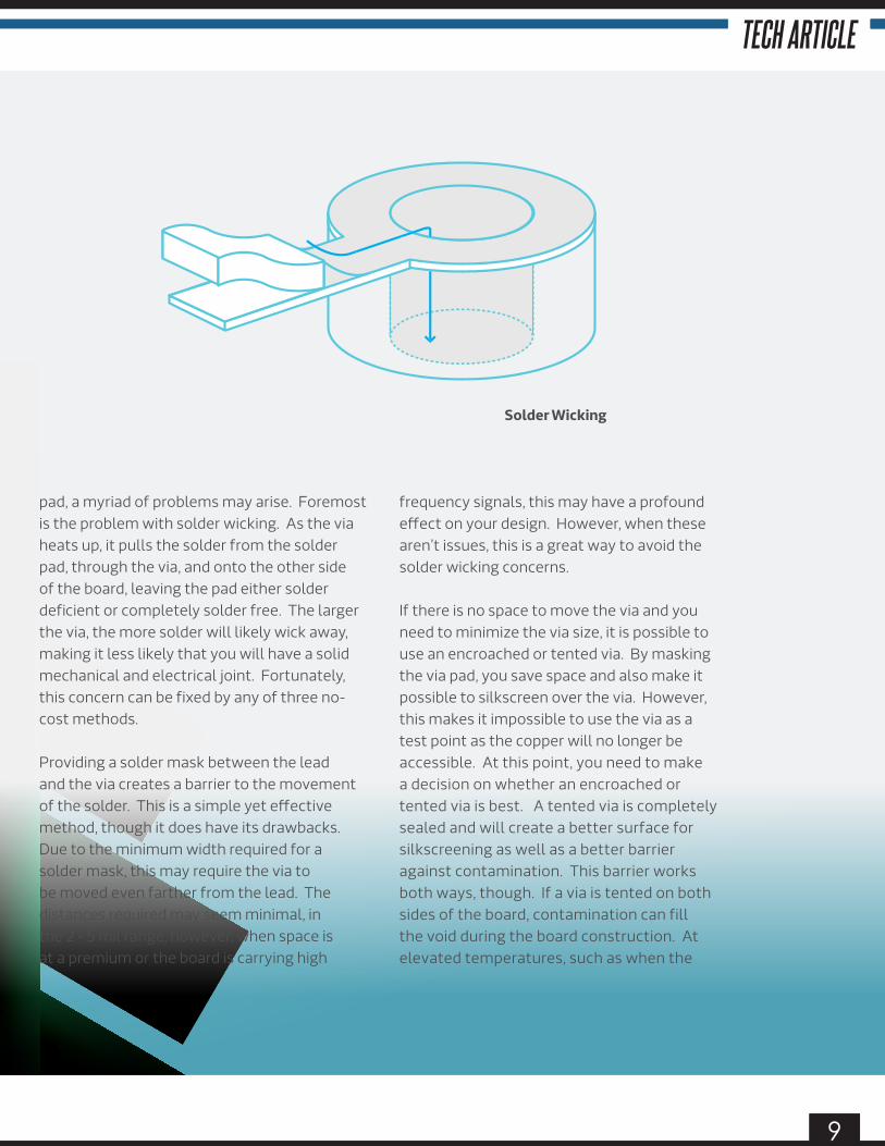
the copper in the via too thin, then the board will expand too much and the copper will break, literally tearing the via apart. In the example above, to get the appropriate aspect ratio with a drill width of 20 mil, this would result in a total pad diameter of 34 mil and allow a max board thickness of 120 mil. Size is important with vias, but location is tantamount. If a via is located close to a solder
pad, a myriad of problems may arise. Foremost is the problem with solder wicking. As the via heats up, it pulls the solder from the solder pad, through the via, and onto the other side of the board, leaving the pad either solder deficient or completely solder free. The larger the via, the more solder will likely wick away, making it less likely that you will have a solid mechanical and electrical joint. Fortunately, this concern can be fixed by any of three no-cost methods.
Providing a solder mask between the lead and the via creates a barrier to the movement of the solder. This is a simple yet effective method, though it does have its drawbacks. Due to the minimum width required for a solder mask, this may require the via to be moved even farther from the lead. The distances required may seem minimal, in the 2 - 5 mil range, however, when space is at a premium or the board is carrying high
frequency signals, this may have a profound effect on your design. However, when these aren’t issues, this is a great way to avoid the solder wicking concerns.
If there is no space to move the via and you need to minimize the via size, it is possible to use an encroached or tented via. By masking the via pad, you save space and also make it possible to silkscreen over the via. However, this makes it impossible to use the via as a test point as the copper will no longer be accessible. At this point, you need to make a decision on whether an encroached or tented via is best. A tented via is completely sealed and will create a better surface for silkscreening as well as a better barrier against contamination. This barrier works both ways, though. If a via is tented on both sides of the board, contamination can fill the void during the board construction. At elevated temperatures, such as when the
6:1Solder WickingAspect Ratio
“If the board is too thick and the copper in the via too thin, then the board will expand too much and the copper will break, literally tearing the via apart.”
99
TECH ARTICLE
The first rule for via design is simple: bigger is better. Larger vias have greater mechanical strength as well as greater electrical and thermal conductivity. While space is always a consideration when it comes to PCB design, vias should have a minimum 20 mil drill width with an annular ring of 7 mil and a minimum aspect ratio of 6:1. For many boards this may be an unacheivable goal, however, the basic premise of bigger is better stands true. When a PCB is exposed to thermal changes in its processing or in its end working environment, the varying coefficient of thermal expansion (CTE) between the laminate and the copper can cause issues. PCBs are constrained through structural latticework to limit horizontal expansion but can expand and contract significantly in the vertical direction. As copper expands and contracts at slightly less than one fourth of the rate of FR-4 laminate, vias are literally being pulled apart every time the board is heated. If the board is too thick and
the copper in the via too thin, then the board will expand too much and the copper will break, literally tearing the via apart. In the example above, to get the appropriate aspect ratio with a drill width of 20 mil, this would result in a total pad diameter of 34 mil and allow a max board thickness of 120 mil. Size is important with vias, but location is tantamount. If a via is located close to a solder
pad, a myriad of problems may arise. Foremost is the problem with solder wicking. As the via heats up, it pulls the solder from the solder pad, through the via, and onto the other side of the board, leaving the pad either solder deficient or completely solder free. The larger the via, the more solder will likely wick away, making it less likely that you will have a solid mechanical and electrical joint. Fortunately, this concern can be fixed by any of three no-cost methods.
Providing a solder mask between the lead and the via creates a barrier to the movement of the solder. This is a simple yet effective method, though it does have its drawbacks. Due to the minimum width required for a solder mask, this may require the via to be moved even farther from the lead. The distances required may seem minimal, in the 2 - 5 mil range, however, when space is at a premium or the board is carrying high
frequency signals, this may have a profound effect on your design. However, when these aren’t issues, this is a great way to avoid the solder wicking concerns.
If there is no space to move the via and you need to minimize the via size, it is possible to use an encroached or tented via. By masking the via pad, you save space and also make it possible to silkscreen over the via. However, this makes it impossible to use the via as a test point as the copper will no longer be accessible. At this point, you need to make a decision on whether an encroached or tented via is best. A tented via is completely sealed and will create a better surface for silkscreening as well as a better barrier against contamination. This barrier works both ways, though. If a via is tented on both sides of the board, contamination can fill the void during the board construction. At elevated temperatures, such as when the
6:1Solder WickingAspect Ratio
“If the board is too thick and the copper in the via too thin, then the board will expand too much and the copper will break, literally tearing the via apart.”

1010
Modern Printed Circuits
PCB is being reflowed or wave soldered, the contamination can outgas and destroy the via and thus the board. When you tent a via, make certain you only do it on one side. An encroached via eliminates this issue by keeping the hole itself open and also has the added benefit versus a tented via of being possible no matter the via size. While tented vias need to be small enough for the solder mask to bridge the drill hole, the encroached via only covers the annular ring and can be as big or small as needed.
Filled vias are also an option, which increase strength, electrical/thermal conductivity, and protect the via from solderwicking and contamination. The main drawback to filled vias is that they can add significant costs to the board. The other methods should have no impact on cost whatsoever.
Every design has different requirements and constraints. However, when possible, utilize these tips by using the largest vias, the appropriate aspect ratio, and by thoughtfully choosing the solder masking style that suits your needs. This will help reduce the overall lifetime costs by increasing reliability of your products.
Solder Dam
Encroached Via
Tented Via
"An encroached via eliminates this issue by keeping the hole itself open and also has the added benefit versus a tented via of being possible no matter the via size."
Content provided courtesy of Advanced Assembly, leader in quick-turn, PCB assembly.For more information on the company, visit www.aa-pcbassembly.com or call 1-800-838-5650.

12
Modern Printed Circuits
Design and AssemblyFor Medical Electronics OEMs
PCB
NexLogic Technologies, Inc. is a one-stop PCB design, fabrication, and assembly electronic manufacturing services (EMS) Provider. As a
leading EMS Provider, it offers total integrated circuit board solutions. The company was established in 1995 and successfully serves over 1,000 customers in North America. Nexlogic’s mission is to provide high quality PCB design and manufacturing processes to a wide swath of OEM markets, ranging from consumer to medical electronics.
EEWeb spoke with Zulki Khan, President and Founder of NexLogic Technologies, Inc., about how his company is meeting the growing and demanding PCB design and assembly requirements of medical electronics OEMs, and the critical aspect of high quality and reliability these OEMs expect.
Interview with Zulki Khan— President and Founder of NexLogic Technologies, Inc.

COVER INTERVIEW
13
Design and AssemblyFor Medical Electronics OEMs
PCB
NexLogic Technologies, Inc. is a one-stop PCB design, fabrication, and assembly electronic manufacturing services (EMS) Provider. As a
leading EMS Provider, it offers total integrated circuit board solutions. The company was established in 1995 and successfully serves over 1,000 customers in North America. Nexlogic’s mission is to provide high quality PCB design and manufacturing processes to a wide swath of OEM markets, ranging from consumer to medical electronics.
EEWeb spoke with Zulki Khan, President and Founder of NexLogic Technologies, Inc., about how his company is meeting the growing and demanding PCB design and assembly requirements of medical electronics OEMs, and the critical aspect of high quality and reliability these OEMs expect.
Interview with Zulki Khan— President and Founder of NexLogic Technologies, Inc.
14
Modern Printed Circuits
What are the key PCB design and assembly challenges facing medical electronics OEMs?
Technology is rapidly advancing. Twenty years ago, hospitals used bulky desktop EKG machines. Today, a trained medical technician can travel anywhere with a portable EKG device that is less than 10 pounds and take your EKG data in less than five minutes. That portable EKG device is based on small PCBs packed with highly advanced electronics. However, the technology doesn’t stop here. The beauty of technology is it constantly advances and evolves. PCB design and assembly is on the front line of these advances. The challenges for PCB design and assembly stem from the fact that medical electronics OEMs continue to demand more features and functionality in an ever-shrinking board area. The design challenges deal with properly managing heat dissipation, placing all the components in smaller
High reliability is of utmost importance to medical electronics OEMs. How should an EMS Provider or Contract Manufacturer (CM) think in terms of providing this high level of reliability to its customers?
First and foremost, medical electronics products across the board cannot afford to have failures whether it’s in the lab or in the field. The burden is on the EMS Provider to assure that these products are designed extremely reliable, and they deliver quality time after time. In effect, the EMS Provider or CM must have quality and reliability imprinted in its DNA. This means quality steps are embedded in the overall design through the assembly and testing process. There must also be a number of well-disciplined quality control (QC) steps within the assembly process to include first article inspection (FAI), automated optical inspection, x-ray, and multiple sets of QC gates along the way. These are all embedded in the process. If you run manufacturing based on a set of disciplined processes, the end result is a medical electronics product that embodies the highest level of quality. On the other hand, when quality is left to inexperience and questionable decisions that assembly personnel make, quality and reliability are severely jeopardized.
What role does experience play in providing the ultra-reliability these OEMs expect?
Vast experience and know-how are at the crux of providing medical electronics OEMs the high reliability they seek. Experience clearly reflects that both PCB design and assembly engineers have honed and continue to hone their skills and know-how over time and have learned great lessons based on inadvertent miscalculations—and they are much the better for it. Along with experience, you also have to blend in a continually growing knowledge about electronics engineering. For example, achieving Certified Interconnect Designer (CID) or CID+ certification plays a major part in successfully dealing with the different aspects of PCB layout, routing, high-speed terminations, impedance control issues, and other related design points.
Another point to make is that when it comes to ultra-reliability and built-in quality, military/aerospace and medical electronics PCBs have similar requirements. When an EMS provider or CM serves both markets, the medical electronics OEM can rest assured that both reliability and quality reign high at that location. In cases like this, there is a healthy interchange and application of reliability and quality actions. As a matter of fact, the
PCB real estate, as well as making sure that all the layout-related DFM issues are taken care of.
Meanwhile, advanced medical electronics products rely on such state-of-the-art device packaging as package-on-package (PoP), flip chip, land grid arrays (LGAs), and tiny passive device packages such as 0201 and 01005 packages. If the EMS Provider or Contract Manufacturer lacks the necessary experience, this newer device packaging can pose significant reliability issues at PCB assembly. There are a number of so-called “quality gates” a PCB assembly house has to pass through to maintain ultra-reliability. That includes complying with the strict medical electronics ISO 13485-quality standard. These aren’t easy assemblies to begin with, but when you factor in ISO 13485’s high quality requirements, you’re adding on another level of challenges.
“The challenges for PCB design and assembly stem from the fact that medical electronics OEMs continue to demand more features and functionality in an ever-shrinking board area.”

COVER INTERVIEW
15
What are the key PCB design and assembly challenges facing medical electronics OEMs?
Technology is rapidly advancing. Twenty years ago, hospitals used bulky desktop EKG machines. Today, a trained medical technician can travel anywhere with a portable EKG device that is less than 10 pounds and take your EKG data in less than five minutes. That portable EKG device is based on small PCBs packed with highly advanced electronics. However, the technology doesn’t stop here. The beauty of technology is it constantly advances and evolves. PCB design and assembly is on the front line of these advances. The challenges for PCB design and assembly stem from the fact that medical electronics OEMs continue to demand more features and functionality in an ever-shrinking board area. The design challenges deal with properly managing heat dissipation, placing all the components in smaller
High reliability is of utmost importance to medical electronics OEMs. How should an EMS Provider or Contract Manufacturer (CM) think in terms of providing this high level of reliability to its customers?
First and foremost, medical electronics products across the board cannot afford to have failures whether it’s in the lab or in the field. The burden is on the EMS Provider to assure that these products are designed extremely reliable, and they deliver quality time after time. In effect, the EMS Provider or CM must have quality and reliability imprinted in its DNA. This means quality steps are embedded in the overall design through the assembly and testing process. There must also be a number of well-disciplined quality control (QC) steps within the assembly process to include first article inspection (FAI), automated optical inspection, x-ray, and multiple sets of QC gates along the way. These are all embedded in the process. If you run manufacturing based on a set of disciplined processes, the end result is a medical electronics product that embodies the highest level of quality. On the other hand, when quality is left to inexperience and questionable decisions that assembly personnel make, quality and reliability are severely jeopardized.
What role does experience play in providing the ultra-reliability these OEMs expect?
Vast experience and know-how are at the crux of providing medical electronics OEMs the high reliability they seek. Experience clearly reflects that both PCB design and assembly engineers have honed and continue to hone their skills and know-how over time and have learned great lessons based on inadvertent miscalculations—and they are much the better for it. Along with experience, you also have to blend in a continually growing knowledge about electronics engineering. For example, achieving Certified Interconnect Designer (CID) or CID+ certification plays a major part in successfully dealing with the different aspects of PCB layout, routing, high-speed terminations, impedance control issues, and other related design points.
Another point to make is that when it comes to ultra-reliability and built-in quality, military/aerospace and medical electronics PCBs have similar requirements. When an EMS provider or CM serves both markets, the medical electronics OEM can rest assured that both reliability and quality reign high at that location. In cases like this, there is a healthy interchange and application of reliability and quality actions. As a matter of fact, the
PCB real estate, as well as making sure that all the layout-related DFM issues are taken care of.
Meanwhile, advanced medical electronics products rely on such state-of-the-art device packaging as package-on-package (PoP), flip chip, land grid arrays (LGAs), and tiny passive device packages such as 0201 and 01005 packages. If the EMS Provider or Contract Manufacturer lacks the necessary experience, this newer device packaging can pose significant reliability issues at PCB assembly. There are a number of so-called “quality gates” a PCB assembly house has to pass through to maintain ultra-reliability. That includes complying with the strict medical electronics ISO 13485-quality standard. These aren’t easy assemblies to begin with, but when you factor in ISO 13485’s high quality requirements, you’re adding on another level of challenges.
“The challenges for PCB design and assembly stem from the fact that medical electronics OEMs continue to demand more features and functionality in an ever-shrinking board area.”
16
Modern Printed Circuits
ISO 13485 medical electronics standard is the equivalent of Mil/Aero J Standard for manufacturing. Both demand tight tolerance controls. EMS companies that serve these specialized markets have all the process details clearly defined and are followed on line after time to achieve optimal results.
What special design-for-manufacturing (DFM) steps need to be taken?
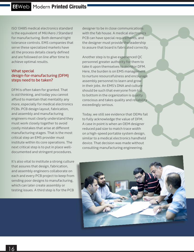
DFM is often taken for granted. That is old thinking, and today you cannot afford to maintain that mentality any more, especially for medical electronics PCBs. PCB design layout, fabrication, and assembly and manufacturing engineers must clearly understand they must work closely together to avoid costly mistakes that arise at different manufacturing stages. That is the most critical step an EMS provider must institute within its core operations. The next critical step is to put in place well-documented and stringent procedures.
It’s also vital to institute a strong culture that assures that design, fabrication, and assembly engineers collaborate on each and every PCB project to keep from sending poor designs to manufacturing, which can later create assembly or testing issues. A third step is for the PCB
designer to be in close communications with the fab house. A medical electronics PCB can have special requirements, and the designer must provide the leadership to assure that board is fabricated correctly.
Another step is to give experienced QC personnel greater authority for them to take it upon themselves to monitor DFM. Here, the burden is on EMS management to nurture resourcefulness and encourage assembly personnel to learn and grow in their jobs. An EMS’s DNA and culture should be such that everyone from top to bottom in the organization is quality conscious and takes quality and reliability exceedingly serious.
Today, we still see evidence that OEMs fail to fully acknowledge the value of DFM. A case in point is when an OEM designer reduced pad size to match trace width on a high-speed portable system design, similar to a medical electronics handheld device. That decision was made without consulting manufacturing engineering.
As a result, a number of issues cropped up at manufacturing. Together with other DFM issues, this design caused manufacturing yields below 60 percent when the goal was above 90 percent.
Why is it so important for medical electronics OEMs to deal with so-called “one-stop-shop” PCB design and assembly houses? What can go wrong when they select separate design and assembly operations?
As I mentioned in my earlier answer, poor communications among design, fabrication, and assembly personnel can lead to disastrous results in manufacturing. Medical electronics OEMs simply cannot jeopardize product quality and reliability, which is their hallmark. Aside from this issue, other major ones deal with time-consuming problem searching, product liability, and traceability, all of which are relatively intertwined.
When a problem occurs, the medical electronics OEM has to spend endless time going from one vendor to another trying to solve that problem. What usually happens in these instances is that each vendor points the finger at the other. That issue has a direct bearing on product liability, time to market, and time to revenue. It’s difficult for the
OEM to pinpoint liability when there are various vendors involved. But when there’s only one design, fab, and assembly house involved, the liability issue becomes a moot point and is quickly resolved. As far as the traceability aspect, again, multiple vendors can create havoc with trying to locate and define date codes, lot codes, and components associated with a given PCB project. With a one-stop shop vendor, the medical electronics OEM can efficiently trace a product problem by quickly pinpointing a failed device and finding out its vendor, lot code, and date code. This gives the medical electronics OEM enormous power. It allows it to quickly and efficiently learn about the problem, recall those projects, and expeditiously fix those issues, if and when they arise.
“PCB design layout, fabrication, and assembly and manufacturing engineers must clearly understand they must work closely together to avoid costly mistakes that arise at different manufacturing stages.”

COVER INTERVIEW
17
ISO 13485 medical electronics standard is the equivalent of Mil/Aero J Standard for manufacturing. Both demand tight tolerance controls. EMS companies that serve these specialized markets have all the process details clearly defined and are followed on line after time to achieve optimal results.
What special design-for-manufacturing (DFM) steps need to be taken?
DFM is often taken for granted. That is old thinking, and today you cannot afford to maintain that mentality any more, especially for medical electronics PCBs. PCB design layout, fabrication, and assembly and manufacturing engineers must clearly understand they must work closely together to avoid costly mistakes that arise at different manufacturing stages. That is the most critical step an EMS provider must institute within its core operations. The next critical step is to put in place well-documented and stringent procedures.
It’s also vital to institute a strong culture that assures that design, fabrication, and assembly engineers collaborate on each and every PCB project to keep from sending poor designs to manufacturing, which can later create assembly or testing issues. A third step is for the PCB
designer to be in close communications with the fab house. A medical electronics PCB can have special requirements, and the designer must provide the leadership to assure that board is fabricated correctly.
Another step is to give experienced QC personnel greater authority for them to take it upon themselves to monitor DFM. Here, the burden is on EMS management to nurture resourcefulness and encourage assembly personnel to learn and grow in their jobs. An EMS’s DNA and culture should be such that everyone from top to bottom in the organization is quality conscious and takes quality and reliability exceedingly serious.
Today, we still see evidence that OEMs fail to fully acknowledge the value of DFM. A case in point is when an OEM designer reduced pad size to match trace width on a high-speed portable system design, similar to a medical electronics handheld device. That decision was made without consulting manufacturing engineering.
As a result, a number of issues cropped up at manufacturing. Together with other DFM issues, this design caused manufacturing yields below 60 percent when the goal was above 90 percent.
Why is it so important for medical electronics OEMs to deal with so-called “one-stop-shop” PCB design and assembly houses? What can go wrong when they select separate design and assembly operations?
As I mentioned in my earlier answer, poor communications among design, fabrication, and assembly personnel can lead to disastrous results in manufacturing. Medical electronics OEMs simply cannot jeopardize product quality and reliability, which is their hallmark. Aside from this issue, other major ones deal with time-consuming problem searching, product liability, and traceability, all of which are relatively intertwined.
When a problem occurs, the medical electronics OEM has to spend endless time going from one vendor to another trying to solve that problem. What usually happens in these instances is that each vendor points the finger at the other. That issue has a direct bearing on product liability, time to market, and time to revenue. It’s difficult for the
OEM to pinpoint liability when there are various vendors involved. But when there’s only one design, fab, and assembly house involved, the liability issue becomes a moot point and is quickly resolved. As far as the traceability aspect, again, multiple vendors can create havoc with trying to locate and define date codes, lot codes, and components associated with a given PCB project. With a one-stop shop vendor, the medical electronics OEM can efficiently trace a product problem by quickly pinpointing a failed device and finding out its vendor, lot code, and date code. This gives the medical electronics OEM enormous power. It allows it to quickly and efficiently learn about the problem, recall those projects, and expeditiously fix those issues, if and when they arise.
“PCB design layout, fabrication, and assembly and manufacturing engineers must clearly understand they must work closely together to avoid costly mistakes that arise at different manufacturing stages.”
18
Modern Printed Circuits
As far as PCB assembly and manufacturing, where should the emphasis be placed so that OEM medical electronics sub-assemblies achieve the highest reliability possible?
As I alluded to earlier, maintaining high quality manufacturing translates directly into high reliability. Emphasis must be placed on the quality steps that are embedded in the assembly and manufacturing process. You are always checking, evaluating, tweaking, and streamlining that process to make it as strong as possible to achieve the reliability medical electronics OEMs demand. That stringent manufacturing process is followed day in and day out. Sometimes, it gets mundane and cumbersome. Quality and reliability come at a price. The price an EMS company pays is to diligently pursue each and every small step, one at a time, to assure attaining quality and the resulting reliability. Here, a top notch and highly experienced reliability manager on the assembly floor is a valuable asset to make sure there are no shortcuts, cutting corners, or short-changing each quality step.
Based on today’s PCB technology trends, what do you foresee for the design and assembly requirements medical electronics OEMs in the future?
In the near term, the roadmap for medical electronics PCBs will be dominated by increasing numbers of small, yet highly complex products sporting the state-of-the-art in technology. The milestones involved will deal with newer packaging and ways to maintain high quality and reliability. This means dealing with smaller, but innovative device packaging that chipmakers will soon develop to meet market demands. At the top of the list is third-level package-on-package or PoP, which means stacking three BGA packaged devices, one on top of another to make the most of valuable PCB real estate. Extremely tiny 0201 and 01005 passive devices are already being used in these products. These minute devices are so small they don’t have sufficient mass or body size to allow placing reference designators on them. As a result, automated optical inspection will have difficulty capturing an image to decipher the right component placement from the wrong one.
Advanced packaging and ever-shrinking PCB real estate will also call for considerably improved PCB cleaning solutions. These devices are so small that the tiniest of flux residue can remain hidden and undetected in a small crevice. That cannot happen in a medical electronics PCB because even the minutest contaminant will cause reliability issues. Advanced packages and assurance of ultra-clean PCBs are definite milestones we will soon encounter.
How can those milestones best be met?
You have to meet these milestones head on with an even stronger mindset and a more disciplined design through assembly process than ever before. Like they say, past experience is the best platform to successfully move forward. In this case, the principles remain the same, although there can be some adjustments and improvements. The point being is the successful EMS Provider dealing with medical electronics OEMs will have to continue to be at the top of its game, be creative, improvise, and not fall victim to complacency. In short, you’ve got to stay ahead of the curve.
“The price an EMS company pays is to diligently pursue each and every small step, one at a time, to assure attaining quality and the resulting reliability. ”

COVER INTERVIEW
19
As far as PCB assembly and manufacturing, where should the emphasis be placed so that OEM medical electronics sub-assemblies achieve the highest reliability possible?
As I alluded to earlier, maintaining high quality manufacturing translates directly into high reliability. Emphasis must be placed on the quality steps that are embedded in the assembly and manufacturing process. You are always checking, evaluating, tweaking, and streamlining that process to make it as strong as possible to achieve the reliability medical electronics OEMs demand. That stringent manufacturing process is followed day in and day out. Sometimes, it gets mundane and cumbersome. Quality and reliability come at a price. The price an EMS company pays is to diligently pursue each and every small step, one at a time, to assure attaining quality and the resulting reliability. Here, a top notch and highly experienced reliability manager on the assembly floor is a valuable asset to make sure there are no shortcuts, cutting corners, or short-changing each quality step.
Based on today’s PCB technology trends, what do you foresee for the design and assembly requirements medical electronics OEMs in the future?
In the near term, the roadmap for medical electronics PCBs will be dominated by increasing numbers of small, yet highly complex products sporting the state-of-the-art in technology. The milestones involved will deal with newer packaging and ways to maintain high quality and reliability. This means dealing with smaller, but innovative device packaging that chipmakers will soon develop to meet market demands. At the top of the list is third-level package-on-package or PoP, which means stacking three BGA packaged devices, one on top of another to make the most of valuable PCB real estate. Extremely tiny 0201 and 01005 passive devices are already being used in these products. These minute devices are so small they don’t have sufficient mass or body size to allow placing reference designators on them. As a result, automated optical inspection will have difficulty capturing an image to decipher the right component placement from the wrong one.
Advanced packaging and ever-shrinking PCB real estate will also call for considerably improved PCB cleaning solutions. These devices are so small that the tiniest of flux residue can remain hidden and undetected in a small crevice. That cannot happen in a medical electronics PCB because even the minutest contaminant will cause reliability issues. Advanced packages and assurance of ultra-clean PCBs are definite milestones we will soon encounter.
How can those milestones best be met?
You have to meet these milestones head on with an even stronger mindset and a more disciplined design through assembly process than ever before. Like they say, past experience is the best platform to successfully move forward. In this case, the principles remain the same, although there can be some adjustments and improvements. The point being is the successful EMS Provider dealing with medical electronics OEMs will have to continue to be at the top of its game, be creative, improvise, and not fall victim to complacency. In short, you’ve got to stay ahead of the curve.
“The price an EMS company pays is to diligently pursue each and every small step, one at a time, to assure attaining quality and the resulting reliability. ”

2020
Modern Printed Circuits
iDesign™
TThere are many crucial elements in the development of an electronic device, but the key to a product’s functionality and longevity is always with circuit protection components. With a plethora of fuses
to choose from—with different values and voltages—there can be an air of uncertainty when selecting the right circuit protection device for your application. Littelfuse, an industry-leading circuit protection company based out of Chicago, recognizes this daunting aspect of circuit design, which is why they developed an online tool that will change the way engineers select circuit protection devices: the iDesign™ Online Fuse Design and Selection Tool. The introduction of iDesign™ marks the first-ever online tool geared towards circuit protection alone, allowing for complex calculation and selection to determine the exact amount of circuit protection needed before going into production. EEWeb got a behind-the-scenes look of Littelfuse’s new tool with Bharat Shenoy, Director of Technical Marketing for the company’s Electronics Business Unit.
The World’s First, Comprehensive
Fuse Selection Toolfrom
Littelfuse
Introducing

21
FEATURED ARTICLE
21
iDesign™
TThere are many crucial elements in the development of an electronic device, but the key to a product’s functionality and longevity is always with circuit protection components. With a plethora of fuses
to choose from—with different values and voltages—there can be an air of uncertainty when selecting the right circuit protection device for your application. Littelfuse, an industry-leading circuit protection company based out of Chicago, recognizes this daunting aspect of circuit design, which is why they developed an online tool that will change the way engineers select circuit protection devices: the iDesign™ Online Fuse Design and Selection Tool. The introduction of iDesign™ marks the first-ever online tool geared towards circuit protection alone, allowing for complex calculation and selection to determine the exact amount of circuit protection needed before going into production. EEWeb got a behind-the-scenes look of Littelfuse’s new tool with Bharat Shenoy, Director of Technical Marketing for the company’s Electronics Business Unit.
The World’s First, Comprehensive
Fuse Selection Toolfrom
Littelfuse
Introducing

2222
Modern Printed Circuits
“We decided to create this tool for a couple of reasons,” Shenoy explained. “The first is that we found that the ‘Search’ function on a lot of websites is too common and too broad.” Parsing through hundreds and even thousands of parts through online parametric search functions can make a hard job even more difficult. After receiving numerous notifications from customers that the search functions weren’t yielding the proper results, Littelfuse felt obligated to begin developing a “smart” fuse design function to make the task more manageable. After considerable time and effort in development, Littelfuse launched the iDesign™ tool, which is free to those who simply register on the iDesign™ site.
The tool is logically separated into tabbed sections—one for each step of the design process. The first tab asks for the initial circuit parameters for the application, whether it is the maximum operating voltage, nominal operating current, maximum operating temperature, and the location of the fuse on the circuit board. These values can be entered manually into each field so the general requirements for the user application can remain throughout the iDesign™ fuse selection process. “For those unfamiliar with designing in fuses, we offer a tutorial section for each search parameter,” Shenoy assures. “If the user is unsure of what the nominal operating current is for their application, we have a tutorial that will hopefully clarify that.”
Application Parameters
Fuse Series Selection
After creating an account, you will be brought to the iDesign™ landing page. The intuitive layout allows users to not only select through a list of fuses, but to read about other parts and actually enlighten the user on some alternate options for their application. For those new to iDesign™ and online design tools in general, there are comprehensive tutorials and slideshows for newcomers to get a feel for the selection and prototyping process. “Many believe that a fuse is a simplistic component or a commodity,” Shenoy explains. “However, it’s not—it can get very complicated with a lot of structures of fuses that give them very different characteristics. If a proper fuse is not selected, it can even be a safety concern.” With iDesign™, Littelfuse is trying to prevent these potential roadblocks for their customers, allowing them an easy starting point for designing in fuses on their boards.
Being the global company that it is, Littelfuse was aware of the fact that the compliance standards for each customer will vary based on their location throughout the world. The safety standards in the “Compliance” section of the tool divides the standards into geographic region—North America, Europe/World, and Asia—to the customer that their safety certification needs are met early on in the process. Once those certifications are selected, the user is brought to the next tab, which deals with the enclosure size of the application you are designing. This section also lets you determine the mechanical structure for the specific type of fuse the user is implementing, whether it is SMD, an axial/cartridge, or radial. Again, the iDesign™ tool provides supplemental material to educate the user on any essential requirements a fuse needs before implementation.
“With iDesign™, Littelfuse is trying to prevent potential roadblocks for their customers, allowing them an easy starting point for designing in fuses on their boards.”

23
FEATURED ARTICLE
23
“We decided to create this tool for a couple of reasons,” Shenoy explained. “The first is that we found that the ‘Search’ function on a lot of websites is too common and too broad.” Parsing through hundreds and even thousands of parts through online parametric search functions can make a hard job even more difficult. After receiving numerous notifications from customers that the search functions weren’t yielding the proper results, Littelfuse felt obligated to begin developing a “smart” fuse design function to make the task more manageable. After considerable time and effort in development, Littelfuse launched the iDesign™ tool, which is free to those who simply register on the iDesign™ site.
The tool is logically separated into tabbed sections—one for each step of the design process. The first tab asks for the initial circuit parameters for the application, whether it is the maximum operating voltage, nominal operating current, maximum operating temperature, and the location of the fuse on the circuit board. These values can be entered manually into each field so the general requirements for the user application can remain throughout the iDesign™ fuse selection process. “For those unfamiliar with designing in fuses, we offer a tutorial section for each search parameter,” Shenoy assures. “If the user is unsure of what the nominal operating current is for their application, we have a tutorial that will hopefully clarify that.”
Application Parameters
Fuse Series Selection
After creating an account, you will be brought to the iDesign™ landing page. The intuitive layout allows users to not only select through a list of fuses, but to read about other parts and actually enlighten the user on some alternate options for their application. For those new to iDesign™ and online design tools in general, there are comprehensive tutorials and slideshows for newcomers to get a feel for the selection and prototyping process. “Many believe that a fuse is a simplistic component or a commodity,” Shenoy explains. “However, it’s not—it can get very complicated with a lot of structures of fuses that give them very different characteristics. If a proper fuse is not selected, it can even be a safety concern.” With iDesign™, Littelfuse is trying to prevent these potential roadblocks for their customers, allowing them an easy starting point for designing in fuses on their boards.
Being the global company that it is, Littelfuse was aware of the fact that the compliance standards for each customer will vary based on their location throughout the world. The safety standards in the “Compliance” section of the tool divides the standards into geographic region—North America, Europe/World, and Asia—to the customer that their safety certification needs are met early on in the process. Once those certifications are selected, the user is brought to the next tab, which deals with the enclosure size of the application you are designing. This section also lets you determine the mechanical structure for the specific type of fuse the user is implementing, whether it is SMD, an axial/cartridge, or radial. Again, the iDesign™ tool provides supplemental material to educate the user on any essential requirements a fuse needs before implementation.
“With iDesign™, Littelfuse is trying to prevent potential roadblocks for their customers, allowing them an easy starting point for designing in fuses on their boards.”
2424
Modern Printed Circuits
2424
Modern Printed Circuits
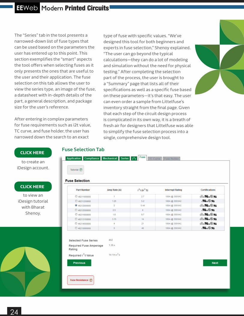
Fuse Selection Tab
The “Series” tab in the tool presents a narrowed-down list of fuse types that can be used based on the parameters the user has entered up to this point. This section exemplifies the “smart” aspects the tool offers when selecting fuses as it only presents the ones that are useful to the user and their application. The fuse selection on this tab allows the user to view the series type, an image of the fuse, a datasheet with in-depth details of the part, a general description, and package size for the user’s reference.
After entering in complex parameters for fuse requirements such as i2t value, TC curve, and fuse holder, the user has narrowed down the search to an exact
type of fuse with specific values. “We’ve designed this tool for both beginners and experts in fuse selection,” Shenoy explained. “The user can go beyond the typical calculations—they can do a lot of modeling and simulation without the need for physical testing.” After completing the selection part of the process, the user is brought to a “Summary” page that lists all of their specifications as well as a specific fuse based on these parameters—it’s that easy. The user can even order a sample from Littelfuse’s inventory straight from the final page. Given that each step of the circuit design process is complicated in its own way, it is a breath of fresh air for designers that Littelfuse was able to simplify the fuse selection process into a single, comprehensive design tool.
to create an iDesign account.
to view an iDesign tutorial
with Bharat Shenoy.
CLICK HERE
CLICK HERE

Sierra Circuits:A Complete PCB Resource
PLUS: The Ground ” Myth in PrintedCircuits
“
PCB Resin Reactor+
Ken BahlCEO of Sierra Circuits
Let There Be
How Cree reinvented the light bulb
LIGHT
David ElienVP of Marketing & Business
Development, Cree, Inc.
New LED Filament Tower
Cutting Edge Flatscreen Technologies
+
+
M o v i n g T o w a r d s
a Clean Energy
FUTURE— Hugo van Nispen, COO of DNV KEMA
MCU Wars 32-bit MCU Comparison
Cutting Edge
SPICEModeling
Freescale and TI Embedded
Modules
ARMCortex
Programming
From Concept to
Reality Wolfgang Heinz-Fischer
Head of Marketing & PR, TQ-Group
Low-Power Design Techniques
TQ-Group’s Comprehensive Design Process
+
+
PowerDeveloper
Octobe r 20 13
Designing forDurability
View more EEWeb magazines— Click Here