
MODELOVÁNÍ MIKROVLNNÝCH REZONÁTORŮ Z METAMATERIÁLŮ · In technical letters, conventional...
48
VYSOKÉ UČENÍ TECHNICKÉ V BRNĚ BRNO UNIVERSITY OF TECHNOLOGY FAKULTA ELEKTROTECHNIKY A KOMUNIKAČNÍCH TECHNOLOGIÍ ÚSTAV RADIOELEKTRONIKY FACULTY OF ELECTRICAL ENGINEERING AND COMMUNICATION DEPARTMENT OF RADIO ELECTRONICS MODELOVÁNÍ MIKROVLNNÝCH REZONÁTORŮ Z METAMATERIÁLŮ MODELING METAMATERIAL MICROWAVE RESONATORS DIPLOMOVÁ PRÁCE MASTER’S THESIS AUTOR PRÁCE Bc. Tomáš Zvolenský AUTHOR VEDOUCÍ PRÁCE prof. Ing. Dr. Zbyněk Raida SUPERVISOR BRNO, 2008
Transcript of MODELOVÁNÍ MIKROVLNNÝCH REZONÁTORŮ Z METAMATERIÁLŮ · In technical letters, conventional...

VYSOKÉ UČENÍ TECHNICKÉ V BRNĚ BRNO UNIVERSITY OF TECHNOLOGY
FAKULTA ELEKTROTECHNIKY A KOMUNIKAČNÍCH TECHNOLOGIÍ ÚSTAV RADIOELEKTRONIKY
FACULTY OF ELECTRICAL ENGINEERING AND COMMUNICATION DEPARTMENT OF RADIO ELECTRONICS
MODELOVÁNÍ MIKROVLNNÝCH REZONÁTORŮ Z METAMATERIÁLŮ MODELING METAMATERIAL MICROWAVE RESONATORS
DIPLOMOVÁ PRÁCE MASTER’S THESIS
AUTOR PRÁCE Bc. Tomáš Zvolenský AUTHOR
VEDOUCÍ PRÁCE prof. Ing. Dr. Zbyněk Raida SUPERVISOR BRNO, 2008


LICENČNÍ SMLOUVA
POSKYTOVANÁ K VÝKONU PRÁVA UŽÍT ŠKOLNÍ DÍLO
uzavřená mezi smluvními stranami:
1. Pan/paní Jméno a příjmení: Bc. Tomáš Zvolenský Bytem: J. Poničana 57, Zvolen, 96001 Narozen/a (datum a místo): 22. dubna 1984 v Prešove
(dále jen „autor“) a
2. Vysoké učení technické v Brně Fakulta elektrotechniky a komunikačních technologií se sídlem Údolní 53, Brno, 602 00 jejímž jménem jedná na základě písemného pověření děkanem fakulty: prof. Dr. Ing. Zbyněk Raida, předseda rady oboru Elektronika a sdělovací technika (dále jen „nabyvatel“)
Čl. 1 Specifikace školního díla
1. Předmětem této smlouvy je vysokoškolská kvalifikační práce (VŠKP):
¨ disertační práce ý diplomová práce ¨ bakalářská práce ¨ jiná práce, jejíž druh je specifikován jako ......................................................
(dále jen VŠKP nebo dílo)
Název VŠKP: Modelování mikrovlnných rezonátorů z metamateriálů Vedoucí/ školitel VŠKP: prof. Ing. Dr. Zbyněk Raida Ústav: Ústav radioelektroniky Datum obhajoby VŠKP: __________________
VŠKP odevzdal autor nabyvateli*:
ý v tištěné formě – počet exemplářů: 2 ý v elektronické formě – počet exemplářů: 2
2. Autor prohlašuje, že vytvořil samostatnou vlastní tvůrčí činností dílo shora popsané a specifikované. Autor dále prohlašuje, že při zpracovávání díla se sám nedostal do rozporu s autorským zákonem a předpisy souvisejícími a že je dílo dílem původním.
3. Dílo je chráněno jako dílo dle autorského zákona v platném znění.
4. Autor potvrzuje, že listinná a elektronická verze díla je identická.
* hodící se zaškrtněte

Článek 2 Udělení licenčního oprávnění
1. Autor touto smlouvou poskytuje nabyvateli oprávnění (licenci) k výkonu práva uvedené dílo nevýdělečně užít, archivovat a zpřístupnit ke studijním, výukovým a výzkumným účelům včetně pořizovaní výpisů, opisů a rozmnoženin.
2. Licence je poskytována celosvětově, pro celou dobu trvání autorských a majetkových práv k dílu.
3. Autor souhlasí se zveřejněním díla v databázi přístupné v mezinárodní síti ý ihned po uzavření této smlouvy ¨ 1 rok po uzavření této smlouvy ¨ 3 roky po uzavření této smlouvy ¨ 5 let po uzavření této smlouvy ¨ 10 let po uzavření této smlouvy
(z důvodu utajení v něm obsažených informací)
4. Nevýdělečné zveřejňování díla nabyvatelem v souladu s ustanovením § 47b zákona č. 111/ 1998 Sb., v platném znění, nevyžaduje licenci a nabyvatel je k němu povinen a oprávněn ze zákona.
Článek 3 Závěrečná ustanovení
1. Smlouva je sepsána ve třech vyhotoveních s platností originálu, přičemž po jednom vyhotovení obdrží autor a nabyvatel, další vyhotovení je vloženo do VŠKP.
2. Vztahy mezi smluvními stranami vzniklé a neupravené touto smlouvou se řídí autorským zákonem, občanským zákoníkem, vysokoškolským zákonem, zákonem o archivnictví, v platném znění a popř. dalšími právními předpisy.
3. Licenční smlouva byla uzavřena na základě svobodné a pravé vůle smluvních stran, s plným porozuměním jejímu textu i důsledkům, nikoliv v tísni a za nápadně nevýhodných podmínek.
4. Licenční smlouva nabývá platnosti a účinnosti dnem jejího podpisu oběma smluvními stranami.
V Brně dne: 30. května 2008
……………………………………….. ………………………………………… Nabyvatel Autor

9
ABSTRAKT
Práce je věnována modelování mikrovlnných rezonátorů z metamateriálů (materiálů se záporným indexem lomu). V úvodu je rozebráno, co metamateriály jsou, jak se vytvářejí a které jejich vlastnosti jsou podstatné při návrhu rezonátorů. Následuje návrh planárního rezonátoru z metamateriálů. Pro tento účel byly naprogramovány funkce počítající rozměry jednotlivých součástí struktury. Simulace navržené struktury probíhala v programu Zeland IE3D.
Simulované struktury byly optimalizovány s ohledem na požadované kmitočty rezonance. První rezonátor sestával z jedné elementární buňky, druhý ze dvou buněk, naladěných na rozdílné kmitočty. Rezonátory byly vyrobeny a experimentálně byly ověřeny jejich vlastnosti.
KLÍČOVÁ SLOVA Metamateriál, rezonátor, levo- a pravotočivý materiál, disperzní charakteristika, prstencový
rezonátor, interdigitální kapacitor, paralelní induktor.
ABSTRACT The project is aimed to modeling microwave resonators from metamaterial (materials with
negative refraction index). First, basics of metamaterials are explained, their creation is described, and their properties essential to the design of microwave resonators are discussed. Second, a metamaterial planar resonator is designed. For this purpose, functions for computing the layout dimensions were programmed. The designed structures were simulated in Zeland IE3D.
Simulated structures were optimized to reach desired resonant frequencies. The first resonator consisted from a single elementary cell, and the second one from two cells tuned to different frequencies. Resonators were fabricated, and their properties were experimentally verified.
KEY WORDS Metamaterial, resonator, left- and right-handed materials, dispersion characteristics, split
ring resonator, interdigital capacitor, shunt inductor.
Bibliografická citace ZVOLENSKÝ, T. Modelování mikrovlnných rezonátorů z metamateriálů. Brno: Vysoké učení technické v Brně, Fakulta elektrotechniky a komunikačních technologií, 2008. 47 s. Vedoucí diplomové práce prof. Dr. Ing. Zbyněk Raida.

10
Prohlášení
Prohlašuji, že svou diplomovou práci na téma Modelování mikrovlnných rezonátorů z metamateriálů jsem vypracoval samostatně pod vedením vedoucího diplomové práce a s použitím odborné literatury a dalších informačních zdrojů, které jsou všechny citovány v práci a uvedeny v seznamu literatury na konci práce.
Jako autor uvedené diplomové práce dále prohlašuji, že v souvislosti s vytvořením této diplomové práce jsem neporušil autorská práva třetích osob, zejména jsem nezasáhl nedovoleným způsobem do cizích autorských práv osobnostních a jsem si plně vědom následků porušení ustanovení § 11 a následujících autorského zákona č. 121/2000 Sb., včetně možných trestněprávních důsledků vyplývajících z ustanovení § 152 trestního zákona č. 140/1961 Sb.
V Brně dne 30. května 2008 ............................................ podpis autora
Poděkování
Děkuji vedoucímu diplomové práce Prof. Ing. Dr. Zbyňkovi Raidovi za účinnou meto-dickou, pedagogickou a odbornou pomoc a další cenné rady při zpracování mé diplomové práce.
V Brně dne 30. května 2008 ............................................ podpis autora

11
Contents 1 Introduction................................................................................................................ 9
2 State of the Art ......................................................................................................... 10 2.1 Composed meta-materials.................................................................................. 10 2.2 Sub-wavelength cavity resonator ....................................................................... 11 2.3 Implementation of metamaterials ....................................................................... 14 2.4 Dispersion analysis of CRLH resonators............................................................ 17
3 Planar CRLH resonators........................................................................................... 20 3.1 Resonator design ............................................................................................... 21 3.2 Steepest descent method .................................................................................... 24 3.3 Results............................................................................................................... 26
4 Simulations versus measurements............................................................................. 31 4.1 Single-cell resonator measurement..................................................................... 32 4.2 Double-cell resonator measurement ................................................................... 34
5 Possible future applications ...................................................................................... 38 5.1 Leaky-wave antenna .......................................................................................... 38 5.2 Microwave components bandwidth enhancement .............................................. 39 5.3 Coplanar waveguide based on split ring resonator.............................................. 40
6 Conclusion ............................................................................................................... 42
References................................................................................................................... 43 List of acronyms and symbols ..................................................................................... 45
List of appendices ....................................................................................................... 47 Appendix 1 – Matlab source code................................................................................ 48
Appendix 2 – One cell structure dimensions ................................................................ 49

9
1 Introduction Today’s communication services are wideband in most cases. Due to the lack of free
frequency bands at the lower part of the frequency spectrum (hundreds of megahertz and units of gigahertz), communication services are shifted to the domain of centimeter- and millimeter-wave frequencies. For simplicity, we will call these bands microwave ones.
The design of microwave resonators belongs to the important areas of microwave engineering. There are two mainly used types of planar resonators – ring resonators and half-wavelength ones [1], [2]. Half-wavelength resonators are usually preferred because of their rather simpler design and geometry that is advantageous when integrating them into complex structures. Line resonators also exhibit better Q factor than ring resonators.
There is a plenty of applications using half-wavelength resonators. E.g., cascaded half-wavelength resonators can operate as a band-pass filter; half-wavelength resonators coupled in parallel can be used often in the oscillator design [3]; etc.
Higher modes suppression belongs to the important aspects of the microwave resonator design. Several methods for higher modes suppression can be used in case of half-wavelength resonators. In case of the transmission zeros method, we adjust electric and magnetic coupling among particular sections of the entire structure in order to regulate the transmission zeros migration and the higher order modes suppression [4].
We have to consider the electromagnetic coupling in case the filter structure consists of more microstrip lines. This coupling influences the selectivity of the whole structure. The stronger the coupling among lines is; the lower the Q factor of the structure we get.
Within the frame of this project, we aspire to solve problems mentioned above by using so called metamaterials for the realization of planar resonators [5], [6].

10
2 State of the Art Forty years ago, the Russian scientist Victor Veselago [7] discussed properties of a
hypothetical material exhibiting the negative index of refraction (all known materials possessed the positive index of refraction). After years of searching, Veselago didn’t manage to find anything with such electromagnetic characteristics and his assumptions faded away.
In early nineties, John B. Pendry in cooperation with scientists in Marconi Materials Technology in England discovered that negative refraction index materials cannot be homogeneous, and have to consist of mini structures. In 2000, David R. Smith with colleagues from California University in San Diego proposed such a composition of materials that exhibited the negative refraction index. This discovery allows us to realize optical lithography microcircuits in nanometer scale and store immense amount of data on optical discs.
In order to understand negative refraction index principles [7], electromagnetic wave propagation through materials has to be studies. Electrons in atoms interact with the wave. This interaction consumes a part of energy of the electromagnetic wave, and influences wave propagation. We can therefore conclude that the creation of imperceptible, but macroscopic structure enables us to control the electromagnetic response of certain materials. The wavelength of waves has to be much higher than the dimensions of macroscopic inclusions.
The material response on electromagnetic waves propagation is described by permittivity and permeability. All of the known materials possess positive values of permittivity and permeability. Alternatively, these properties can be described by the index of refraction [7]:
µε ⋅=n , (2.1)
where, ε and μ are relative permittivity and permeability of some material. Because of the square root, refraction index of any material has to be a positive value. But Veselago pointed out, that refraction index has to be a negative value, if permeability and permittivity are negative. Negative ε or μ means, that electrons are moving in an opposite direction related to the force causing their movement.
2.1 Composed meta-materials Resonance is the key factor for achieving the negative refraction index. In case of meta-
materials the negative index is achieved artificially by raised small circuits, designed to emulate magnetic or electric circuit responses.
Propagating through a material, velocity of wave is decreased by its refraction index, and we can write [19]:
ncv = , (2.2)
where c is velocity of light and n denotes the refraction index.
In case the refraction index n is negative the wave is propagating backwards. In order to understand this phenomenon, we have to understand the difference between the phase and group

11
velocity. The phase velocity describes the changes of the phase. The group velocity describes the propagation of the energy. Definitions of group and phase velocity are [19]:
dkdvgω
= , (2.3)
k
v pω
= . (2.4)
Here, ω is angular frequency and k denotes wave number.
Phase and group velocities can differ. Veselago discovered that these velocities are anti-parallel in metamaterials [7].
2.2 Sub-wavelength cavity resonator In technical letters, conventional materials are called right-handed (RH) ones, and materials
exhibiting the negative refraction index are called left-handed (LH) ones, or backward media. In this section, we will try to generalize the EM wave propagation through combined RH and LH media [5].
The structure analyzed is a simple cavity resonator (Fig. 1) composed of two layers (a RH one and a LH one). The layers are placed between two conductive layers – reflectors.
Fig. 1 1D cavity resonator composed of RH (left) and LH (right) layer
placed between two reflectors; adopted from [5].
The problem of solving Maxwell’s equations is generalized by assuming that intrinsic impedances of layers are not the same as η0, i.e. η0 ≠ η1 ≠ η2. Assuming the 1D cavity resonator structure from Fig. 1, all the quantities are independent on the x and y coordinates. Conductive plates are located at z = 0 and z = d1 + d2. In the range of the conventional material (0 < z < d1) magnetic and electric field can be described by following expressions [5]:
( )zknEEx 01011 sin= , (2.5)

12
( )zknEj
knH y 01011
011 cos
ωµ= . (2.6)
Numbers 1 and 2 stand for quantities in the regions of materials with thicknesses d1 and d2, where n is material refraction index, E01 is wave amplitude while propagating through the layer with the thickness d1, ω is angular frequency, μ1 is material permeability and the argument of sin and cos are harmonic components of wave – k0 is free space wave number and z is the coordinate of the wave propagation.
In the range of the metamaterial with the negative relative permittivity and permeability (d1 < z < d1 + d2), fields can be described by expressions [5]:
( )[ ]zddknEEx −+= 2102022 sin , (2.7)
( )[ ]zddknEj
knH y −+−= 2102022
022 cos
ωµ , (2.8)
To satisfy the boundary conditions between the layers d1 and d2 we can write [5]:
11
|| 21 dzxdzx EE == = , (2.9)
11
|| 21 dzydzy HH == = . (2.10)
This means that wave components should have the same values at the boundary of two environments. If the boundary conditions noted above are fulfilled, the residual of Ex1|z=d1 and Ex2|z=d1, and the residual of Hy1|z=d1 and Hy2|z=d1 is zero [5]:
( ) ( ) 0sinsin 2020210101 =− dknEdknE , (2.11)
( ) ( ) 0coscos 202022
210101
1
1 =+ dknEndknEnµµ
. (2.12)
In order to get a nontrivial solution of these equations (E01 ≠ 0 and E02 ≠ 0), the determinant of (2.11) and (2.12) has to be zero [5]:
( ) ( ) ( ) ( ) 0sincossincos 2021011
1101202
2
2 =+ dkndknndkndknnµµ
. (2.13)
After dividing (2.13) in order to get the tan functions, we obtain [5]:
( ) ( ) 0tantan 2021
1101
2
2 =+ dknndknnµµ
. (2.14)
In this dispersion relation, either the sings of n1 and n2 are positive or negative; anything about the resulting balance of the equation (2.14) is changed.
The first layer d1 is assumed to be a conventional lossless material (ε1 > 0 and μ1 > 0), while the second layer is considered to be a lossless metamaterial (ε2 < 0 and μ2 < 0). Then we can write μ1 = |μ1| and μ2 = – |μ2|. Putting this into (2.14) we get [5]:
( ) ( ) 0tantan 2021
1101
2
2 =+− dknndknnµµ
. (2.15)

13
This equation can be transformed to the thicknesses condition [5]:
( )( )202
101
12
21
tantan
dkndkn
nn
=µµ
. (2.16)
This relation determines the thicknesses ratio. Principally, thicknesses of layers can be any size as long as the ratio of tangent of these thicknesses is fulfilled. Moreover, we can simplify (2.16) for small arguments (if d1, d2 and ω are properly chosen) [5]:
2
1
1
2
dd
≅µµ
. (2.17)
Equation (2.17) shows that a nontrivial solution of (2.11) and (2.12) covers the ratio of thicknesses instead of their sum. For a given frequency, we can get a sub-wavelength cavity resonator if the second layer has negative permittivity and permeability.
At the frequency 4 GHz, the half-wavelength resonator is 37.5 mm (considering a conventional air cavity resonator). If the material of a negative permittivity –0.5 ε0 and a negative permeability –0.5μ0 is used as the LH part, and the air with ε0 and μ0 is used as the RH part, then n1 = 1, and n2 = 0.5, and the required ratio of thicknesses equals to 0.5. Consequently, we can make the meta-material part λ0/10 thick, and the air part should have the thickness λ0/20 (where λ0 is free space wavelength). Overall thickness of such a composed cavity would be 3λ0/20, what gives the length 11.25 mm instead of 37.5 mm for the conventional air cavity.
Let us to concentrate now on the design of resonators with the sufficient Q factor and utmost higher modes spacing (resonant frequencies). In order to design such a resonator, we can use an electromagnetic material exhibiting a negative permittivity and a negative permeability at some frequencies. This means that the direction of the Poyinting vector (the direction of the power flow) is anti-parallel compared to the orientation of the phase velocity vector. Considering conventional materials, the direction of the Poyinting vector and the phase velocity vector are identical.
Fig. 2 shows a material, where a layer of the thickness d1 is a conventional material, and a layer of the thickness d2 is a meta-material. Arrows S1 and S2 show directions of the Poyinting vector, arrows k1 and k2 are directions of the phase velocity.
Resonators designed and investigated in this project are composed of both the LF and RH transmission lines. Such resonators are called CRLH TL (Composite Right/Left Handed Transmission Lines). Designing such a resonator in the planar form, LH TL is replaced by series capacitors and shunt inductors. The resonator exhibits then a nonlinear phase response. The phase response can be further shaped according to our requirements by changing properties of transmission lines (adjusting RH TL length and changing inductance and capacity of LH TL).
Decreasing the slope of the phase response, better higher modes spacing can be reached. Increasing the slope of the phase response, we get the resonator exhibiting higher Q factor. The advantage of this technique is hidden in the fact that changing the phase response influences both the essential parameters of resonators – the selectivity and the higher modes spacing.

14
Fig. 2 The resonator consisting of the left-handed layer (right)
and the right-handed layer (left); adopted from [5]. In the next sub-chapter, approaches to composing metamaterials are reviewed.
2.3 Implementation of metamaterials Several scientific groups have focused on composing metamaterials from the periodic thin
wire media. Because of the lack of the magnetic charge analogous to the electric charge, achieving a negative permeability is more difficult than producing a negative permittivity. On the contrary, the negative permittivity can be achieved by using a thin wire periodic media.
For the experimental verification of the properties of metamaterials, so called split ring resonators (SRR) were designed (see Fig. 3a), which exhibit a large magnetic response in a certain frequency range. When measuring a frequency response of a metamaterial, which is composed from split ring resonators and periodic thin wires (Fig. 3c), stop band can occur in the characteristic. Stop bands can be caused by the following phenomena:
• The structure can have electric resonances, and electromagnetic waves cannot propagate through the structure because of the negative value of the effective permittivity.
• Magnetic resonances of the structure hinder the wave propagation. The uncertainty of the cause of occurring the stop band can be removed by using a structure, where ring resonators are closed (CSRR) as depicted in Fig. 3b. The magnetic resonance is removed by closing the resonator’s structure, and electrical resonance remains. We can therefore expect to have a pass band in the place of a stop band at the frequencies for the negative permeability.

15
Fig. 3 a) SRR – split ring resonator, b) CSRR – closed split ring resonator,
c) periodic meta-material composed (CMM) of SSR and wires on the other side of the substrate; adopted from [12].
The transmission characteristics of the structure composed from SRR and CSRR are depicted in Fig. 4. Obviously, in the place of the stop band (3.5 to 4 GHz) of the SRR structure, the pass band of the CSRR structure appears which indicates permeability of the negative value.
Another stop band appears at higher frequencies in both curves. Therefore, the stop band cannot be automatically considered to be an indicator of the negative permeability.
Split ring resonators have some disadvantages like bi-anisotropy, or the electric field excitation of the magnetic resonance. These disadvantages can be removed by using a labyrinth structure which is composed of four, instead of two rings (see Fig. 5). The ambiguity in the transmission characteristics (similar to the simple SRR structure) can be removed by using the closed SSR structure.
Fig. 4 Measurement results for SRR and CSRR medium; adopted from [12].

16
Fig. 5 a) labyrinth split ring resonator, b) a fabricated structure; adopted form [12]
Another proof of the left handed character of the material considers the phase velocity, which should be negative in a certain frequency range. The negative phase velocity can be verified experimentally as shown in Fig. 6. Horn antennas act here as a source and a receiver, ranged 13 cm (source) and 70 cm (receiver) form the CMM. The CMM is of the form of a wedge structure with the slope angle 26°. Measurement of the phase is performed on rectangular slabs of the left-handed materials with a varying number of layers. We can see the phase of the transmitted signal in the right-handed region in Fig. 7a, where dashed lines represent its phase, when propagating through the material composed of more layers. Obviously, the phase is rising with the number of layers rising. Fig. 7b shows the phase of the received signal (in the left-handed region of frequencies), again for different number of layers.
We can observe the inverse effect of growing the number of layers: the phase of the received signal is actually decreasing with increasing the number of layers of CMM, which indicates a typical left-handed behavior. Operating with the phase shifts of consequent numbers of layers, we can calculate the refraction index. The phase velocity can be defined as (2.2) and (2.4), and thus the refraction index can be defined as [13]:
ω
ckn ⋅= , (2.18)
dldk φ
= , (2.19)
where n is material’s refraction index, k denotes the wave number, c is the light velocity, and ω is the angular frequency. Then we get refraction index as [13]:
dldcn φ
ω⋅= . (2.20)
The average phase shift between the odd parts of the resonator structure is –0.41 ± 0.5π. The refraction index given by (2.18) is approximately –1.87 ± 0.05.

17
Fig. 6 a) CMM wedge structure, b) measuring items setting; adopted form [13].
Fig. 7 a) RH phase shift, b) LH phase shift; adopted form [13].
This moment, we understand the basic principles of the metamaterial resonators, and we have a basic notion about their implementation. In the next step, the dispersion analysis has to be discussed in order to characterize the metamaterial resonators.
2.4 Dispersion analysis of CRLH resonators Parameters of the microstrip resonator (mode spacing and the Q factor) depend on the
relation between the phase and the frequency φ(f). From the frequency dependence of the phase response, we can calculate the phase constant [6]:
( ) ( )dff φ
β −= . (2.21)
Here, d is the overall length of the transmission line. This way, we can analyze the resonator using the dispersion ratio. In Fig. 8, we can see the dispersion diagram of the conventional microstrip transmission line. Considering a ring resonator composed of a microstrip of the length d, the ring will resonate at mode fR,1, for which phase response φ(fR,1) will be –2π, and so β = 2π/d. Resonant frequencies are denoted fR,m, where m means the order of resonance. Higher order modes occur, if the phase equals to integer multiples of 2π.
Fig. 8 demonstrates that the dispersion response of the conventional transmission line is linear. Obviously, the conventional microstrip line can resonate at the integer multiples of fR,1. Defining higher modes spacing as the ratio of the second resonant frequency to the first one, we obtain the value 2 for the conventional TL. A relatively unchanging slope causes the invariance

18
of the Q factor. This linear characteristic does not enable to significantly change parameters of the transmission line. However, if we are able to influence the dispersion slope, we are capable to control the mode spacing and the Q factor. This aim can be reached by using CRLH TLs.
Fig. 8 Dispersion diagram of a conventional Fig. 9 Dispersion diagram of a CRLH microstrip line; adopted from [6]. TL; adopted from [6].
CRLH TL is modeled by the segment of RH TL (parallel capacity and serial inductivity) and by the segment of LH TL (parallel inductivity and serial capacity). The RH part is being realized by a conventional microstrip line and the LH part by gap capacitors and shunt inductors. The dispersion diagram of this folded CRLH TL can be seen in Fig. 8. There are four resonances, which determine the dispersion character [6] of the structure:
( )LL
dLH CLff
πβ π
41
≈−== , (2.22)
( )RL
parallel CLff
πβ
210 ≈== , (2.23)
( )LR
serial CLff
πβ
210 ≈== , (2.24)
( )RR
dRH CLff
πβ π 1
≈−== . (2.25)
Frequencies fparallel and fserial are resonant frequencies of shunt or serial components. If characteristic impedances of RH and LH are equal, the structure is balanced. Out of this condition, the equality of fparallel and fserial also emerges.
In equations (2.22) to (2.25), LL is inductance of a shunt inductor of LH part, CL denotes capacity of series capacitor of LH part, CR is a shunt capacitor capacitance of RH part, and LR denotes series inductor inductance of RH part.

19
The resonance at the lower frequencies is called LH mode (group and phase velocity are anti-parallel); fLH is the lower cutoff frequency specified by LH components. The resonance at the higher frequencies is called RH mode (group and phase velocity are parallel); fRH is the upper cutoff frequency specified by RH components.
The conventional TL resonates at frequencies depending on index values m = 1, 2, … only, while the CRLH resonator can resonate at frequencies depending on index values m = –2, –1, …, 0, …, 1, 2. That is given by the fact, that the phase constant can be positive, negative or zero. Using the equation [6]:
( ) ( )Nd
ff φβ −= , (2.26)
we can decide, what resonant frequencies for periodic structures can be excited. In (2.26), N denotes the total number of sections of the periodic resonator structure, and d is the length of unit cell. There are N+1 possible resonant frequencies for both the modes RH and LH, including resonances of the zero order if the structure is unbalanced.
Comparing the dispersion diagram of a conventional resonator and a CRLH one, the CRLH resonator exhibits a nonlinear phase constant that can be alternated by changing values of components of LH and RH segments. That means, we can change the mode spacing and the Q factor by the variation of parameters CL, CP, LS a LL, and also by changing N.
In the next chapter, all the principles reviewed in the chapter 2 are going to be applied to the design of a planar resonator based on the combination of the conventional right-handed structure and the metamaterial left-handed structure.

20
3 Planar CRLH resonators A conventional microstrip line is a right-handed medium, which can be modeled by
a longitudinal inductivity and a transversal capacity. If such a structure is completed by a serial capacity and a parallel inductivity, a composed left/right handed structure. A potential implementation of such a structure was proposed in [6].
Fig. 10 CRLH microstrip resonator and its circuit model; adopted from [6].
In Fig. 10, we can see a planar resonator setup and its circuit model. The setup consists of a microstrip transmission line, a gap capacitor and a shunt inductor. For lumped components of the circuit model, following values were considered: Lstub = 0.16 nH, Cgap = 0.32 pF. The length of the microstrip transmission line was set to L = 2.25 cm. The corresponding dispersion diagram is depicted in Fig. 11.
Fig. 11 Dispersion diagram for microstrip Fig. 12 Transmission coefficient for CRLH resonator; adopted form [6]. CRLH resonator; adopted form [6].

21
In order to verify results published in [6], the circuit model of the resonator was simulated in Matlab (see Fig. 13).
Fig. 13 Dispersion diagram for the Matlab model of the planar CRLH resonator.
In [6], the resonator consisting of four cascaded cells was studied. Symbolic transfer function of such structure is rather complicated, and therefore, our simulation was performed for a single cell. This simulation was aimed to reach a similar shape of the dispersion diagram and its negative part dominantly. That way, the possibility of realizing a similar structure should be verified. Fig. 13 approves validity of the model.
3.1 Resonator design In the next step, the circuit model of the resonator was transformed to the form of the
planar microwave circuit in order to verify the expected properties of the metamaterial resonator. For the implementation, we chose the hardware solution published in [6]. Parameters of this resonator are determined at the following resonant frequencies:
Fig. 14 Resonator design properties; adopted from [6].

22
GHz7.43, =−Rf , GHz85.42, =−Rf , GHz15.51, =−Rf , GHz35.50, =Rf , GHz61, =Rf , GHz5.62, =Rf , GHz05.73, =Rf , GHz55.74, =Rf .
Since [6] did not contain any information about the dimensions of the planar layout of the circuit and the substrate used, the dimensions of the planar structure had to be computed to reach the gap capacities Cgap = 0.32 pF, and the shunt inductances Lstub = 0.16 nH. Therefore, a proper dielectric substrate was chosen, and Matlab functions were developed to synthesize the described capacities and inductances.
Using a conformal projection, the relation for computing the effective permitivity εef can be obtained [2]:
refr εε
ε≤≤
+2
1 , (3.1)
where εr is the dielectric constant of the substrate.
If the metallization thickness correction is going to be considered when computing εef, the following expressions can be used [2]:
hw
hthw r
wh
rref /
/6.4
1104.01211
21
21 2
⋅−
−
−⋅+
⋅+⋅
−+
+=
εεεε (3.2)
for 1/ ≤hw ,
hw
htr
wh
rref /
/6.4
11211
21
21
⋅−
−⋅+
⋅−
++
=εεε
ε (3.3)
for 1/ ≥hw .
In (3.2) and (3.3), h is the height of a substrate, w denotes the width of the transmission line, and t is the thickness of a TL metallization. For t = 0 (the metallization thickness is negligible), the error of the approximation is maximally 1 %.
Fig. 15 Interdigital capacitor structure.

23
In the following steps, the computed effective permittivity of the substrate is used to design the serial capacitor of the required capacity, and the parallel inductor of the desired inductivity.
First, we tried to program an iteration function for the calculation of a gap capacitor as used in [6], but for the chosen substrate, a satisfactory high capacity for realistic layout dimensions was not obtained. Using [2], we therefore implemented in Matlab an iteration function for an inter-digital capacitor.
Fig. 16 Circuit model of the inter-digital capacitor.
In case wp = s = x, parameter of the elements of the circuit model of the inter-digital capacitor can be computed using the following relations [2]:
( )[ ]2131 AAnlw
C rs +⋅−⋅⋅
+=
ε , (3.4)
nw
RlRP
SSER ⋅⋅
⋅⋅=
34 . (3.5)
Here, n is the number of capacitor’s fingers, w is the width of the whole capacitor, l denotes the length of one finger, RS is a serial resistance of the capacitor (see Fig.16) and wp denotes the width of one finger. In [2], coefficients A1 and A2 are given in the form of the charts. These charts were approximated by the analytical expressions:
21
1 15287116.03349057.04.25
1
⋅−⋅=
−
xhA [pF; mm] (3.6)
21
2 22820444.050133101.04.25
1
⋅−⋅=
−
xhA [pF; mm] (3.7)
These expressions are valid for 3 ≤ h/x ≤ ∞. The symbol x actually denotes s what is the gap width. The bottom side of the substrate is assumed to be metallized.
The description of the source code for the capacitance calculation is given in Appendix 1. Dealing with the shunt inductor used for this model, the following expressions can be used
assuming ZL >> ZV, and l << λg [2]:
c
lZL efL ε⋅⋅
= , (3.8)
lZcR L ⋅⋅⋅⋅= β2 (3.9)

24
In (3.8) and (3.9), ZV is the characteristic impedance of the transmission line, and ZL is the characteristic impedance of the shunt, l denotes the length of the shunt, εef is the effective permittivity of the transmission line of the shunt, c is the light velocity, and β is the attenuation constant of the shunt.
Fig. 17 Shunt inductor.
The inductor exhibits the lumped character if l << λg/32, so frequency margin is [2]:
ef
MAX lcf
ε⋅⋅=
32 (3.10)
The inductance of the metallized via or the strip on the edge of the substrate can be computed according to the expression [2]:
( )
+−⋅+
++⋅⋅= 22
220 5.1ln
2hrr
rhrhhLVIA π
µ , (3.11)
where h is the thickness of the substrate, and r is the radius of the metallized via.
The parasitic resistance of the metallized via can be computed using the relation [2]:
δffRR SS +⋅= 1 , (3.12)
where
20
1t
fC ⋅⋅⋅
=σµπδ , (3.13)
and RSS is the specific high-frequency resistance, f denotes frequency at which R is calculated, σC denotes the conductivity of the material used, and µ0 is permeability of vacuum.
The Matlab files are enclosed to this report on a CD attached.
3.2 Steepest descent method For the calculation of all the parameters needed to model the whole structure, dimensions
of capacitors and inductors exhibiting the required inductance and capacitance and substrate have

25
to be computed. In the developed Matlab functions, computations are performed iteratively using the steepest descent method.
The steepest descent method [8] is an algorithm for finding the nearest local minimum of a function by calculating the gradient of a function. The gradient [9] expresses an increment of a scalar function dφ. In Cartesian coordinates:
( )ZYXZYX udzudyudxu
zu
yu
x
dzz
dyy
dxx
d
⋅+⋅+⋅⋅
⋅+⋅+⋅=
⋅+⋅+⋅=
δδφ
δδφ
δδφ
δδφ
δδφ
δδφ
φ
(3.14)
At the beginning, the position of the minimum of the function has to be estimated. From the starting point P0, the minimum estimation moves from Pi to Pi+1 in the direction against the local gradient.
If the method is applied to a one-dimensional function, we obtain [8]:
( )iiii xfxx '1 ⋅∋−=+ , 1≤∋i , (3.15)
where f’(xi) is the local gradient and i∋ is the length of the step towards the minimum of such value. If i∋ is properly chosen, then the value of the objective function is significantly decreased. High or low value of i∋ decides the quickness of the convergence (or the divergence). A lower value of the step provides a better stability of the algorithm.
Graphical interpretation of this method is depicted in Fig. 18.
Fig. 18 Steepest descent method; adopted from [9].

26
The Matlab files are enclosed to this report on a CD attached.
3.3 Results The described design procedure was applied to the design of a single-cell resonator and a
double cell one. In both the cases, resonators were designed for the dielectric substrate Arlon D600 (the height h = 1.54 mm, the dielectric constant εr = 6.15, and the loss factor tan δ = 0.003).
The layout of the single-cell resonator is depicted in Fig. 19. For the resonant frequency fr = 6.0 GHz, obtained dimensions are described in detail in appendix 2 (page 49).
The cell is consists of two serial inter-digital capacitors and shunt inductors, connected to the ground by the metallized through vias. The Matlab files are enclosed to this report on a CD attached.
For the initial verification of the design, numerical analysis of the resonator in Zeland IE3D was performed. Zeland IE3D [10] is a full-wave electromagnetic solver, which solves Maxwell equations in the integral form. IE3D is very accurate. There are no limitation related to the grids uniformity and the shape of the structures.
In the standard layout editor, the analyzed structure was composed from polygons. After the layout is completed, simulation parameters have to be set (the number of wavelengths per the maximal simulation frequency, more frequency steps for higher accuracy and smooth curves, etc.). Thanks to the AIF (Advanced Intelli Fit), curves can be fitted employing mathematical and physical principles (a detailed frequency response of a complicated structure with many resonances can be extracted by using simulation results at a few frequency points only, and therefore, the simulation can yield accurate results in just 10% of the expected simulation time).
Fig. 19 Single-cell resonator.
Results achieved for the single-cell resonator in the frequency range from 4.5 GHz to 7.5 GHz are depicted in Figures 20 to 22. Figures differ in the number of samples per wavelength (from 10 to 15), in using the Advanced Intelli-Fit technique, and in the number of the frequencies of analysis (from 80 to 200).

27
Fig. 20 Simulation results of the single-cell resonator tuned at 6 GHz. Frequency steps: 80, samples per wavelength (fMAX): 12, AIF: disabled.
Fig. 21 Simulation results of the single-cell resonator tuned at 6 GHz.
Frequency steps: 150, samples per wavelength (fMAX): 15, AIF: enabled.

28
Fig. 22 Simulation results of the single-cell resonator tuned at 6 GHz.
Frequency steps: 200, samples per wavelength (fMAX): 10, AIF: disabled.
Simulation results pictured contain a number of resonant-like points. The points can be identified as local maxima of the transmission coefficient frequency response. In Figures 20 to 22, the resonant-like points are indicated by numbered triangles. Numerical values of the resonant-like frequencies are summarized in Table 1. For various simulation settings, slightly different results are obtained. However, the resonant frequencies we are interested in are very similar.
figure freq. steps
sampl. per λ AIF 1 2 3 4 5 6 7
20 80 12 no 5.06 5.31 6.04 6.56 6.99 7.67 5.18
21 150 15 yes 4.40 4.95 5.07 6.06 6.54 7.00 7.76 22 200 10 no 4.86 5.07 5.31 5.99 6.52 7.01 6.11
Tab. 1 Computed resonant-like frequencies of single-cell resonator tuned at 6 GHz.
Considering simulation results obtained for the single-cell resonator (tuned at 6 GHz), following conclusions can be formulated:
• The frequency of the minimum reflections and maximum transmission varies from 6.04 to 6.11 GHz. Hence, the difference between results is about 1 %.
• Since the analyzed structure is reciprocal, frequency responses of s11 and s22 should be identical. Figures 20 and 21 do not meet this condition in resonances (5 dB difference in Fig. 20, and 15 dB difference in Fig. 21).

29
• The value of the reflection coefficient s11 in the main resonance varies from –10 dB to –15 dB. The value of the reflection coefficient s22 in the main resonance varies from –20 dB to –25 dB. Hence, the impedance matching of the single-cell resonator can be considered as satisfactory.
• The value of the transition coefficient s21 in the main resonance stays fixed about –15 dB. This value is unacceptably low.
• In Fig. 22, some values of s11 and s22 are higher than 0 dB. Since the resonator is a passive circuit, the results indicate an error in computations (probably a very low number of samples per wavelength).
In the next step, the design and the simulation procedures were repeated for the double-cell resonator:
• The resonator was designed for the substrate Arlon D600 (the height h = 1.54 mm, the dielectric constant εr = 6.15, and the loss factor tan δ = 0.003) again.
• The first cell of the resonator was identical with the cell of the single-cell resonator.
• The second cell of the resonator was tuned to have the main resonance at the frequency 6.5 GHz in order to widen the bandwidth of the filter. Corresponding dimensions of the second cell are described in detail in appendix 2 (page 49).
Fig. 23 Simulation results of the single-cell resonator tuned at 6.5 GHz. Frequency steps: 80, samples per wavelength (fMAX): 12, AIF: disabled.
30
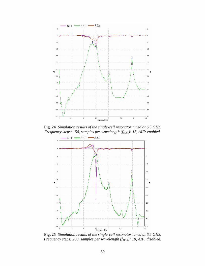
Fig. 24 Simulation results of the single-cell resonator tuned at 6.5 GHz. Frequency steps: 150, samples per wavelength (fMAX): 15, AIF: enabled.
Fig. 25 Simulation results of the single-cell resonator tuned at 6.5 GHz. Frequency steps: 200, samples per wavelength (fMAX): 10, AIF: disabled.

31
figure freq. steps
sampl. per λ AIF 1 2 3
23 80 12 no 6.49 7.02 7.96
24 150 15 yes 6.35 7.01 7.94 25 200 10 no 6.51 7.03 7.97
Tab. 2 Computed resonant-like frequencies of single-cell resonator tuned at 6.5 GHz.
Considering simulation results obtained for the single-cell resonator (tuned at 6.5GHz), following conclusions can be formulated:
• The frequency of the minimum reflections and maximum transmission varies from 6.35 to 6.51 GHz. Hence, the difference between results is about 2 %.
• Analyzed structure is semi-symmetrical (see appendix 2), hence frequency responses of s11 and s22 are slightly different in resonances and near them. Differences in s11 and s22 are 16 dB for Fig. 23, 6 dB for Fig. 24 and 28 dB for Fig. 25).
• The value of the reflection coefficient s11 in the main stays fixed about –5 dB. The value of the reflection coefficient s22 in the main resonance varies from –10 dB to –33 dB. Since the structure is rather symmetrical, poor values of s11 are probably the cause of error in computations.
• The value of the transition coefficient s21 in the main resonance stays fixed about –5 dB. This value is acceptable.
• In Fig. 23 and 25, some values of s11 and s22 are higher than 0 dB. Since the resonator is a passive circuit, the results indicate an error in computations (probably a very low number of samples per wavelength).
In final, both the resonator cells were connected together. Simulation results, and their comparison with measurements, are presented in the next chapter.
4 Simulations versus measurements Experimental data were obtained using a scalar analyzer Anritsu 54147A. Parameters of the
analyzer are summarized Tab. 3. The analyzed circuit was connected to the analyzer according to the Fig. 26.
Fig. 26 Measurement schematics.

32
In the first step, the single-cell resonator was measured and compared to the simulation results. In the second step, the procedure was repeated for the double-cell resonator.
Frequency range 10 MHz ÷ 20 GHz (crystal) Dynamic range (analyzer) -55 dBm ÷ +16 dBm
Inputs 2 standard inputs A and B Display resolution horizontal 51, 101, 201 or 401 points, vertically 0.025 dB, 0.0025 ns
Frequency step 200 kHz
Sensitivity 0.1 dB(m) ÷ 10 dB(m) per segment, independently adjustable channels 0.1 ÷ 100 ns per segment
Sweep time one run 70 ms for resolution 101 points, while using averaging and smoothing 130 ms
Power setting accuracy 1 dB, while using 75 Ω load ±1.2 dB
Output power max 10 dBm for 50 Ω load
Tab. 3 Anritsu 54147A parameters.
4.1 Single-cell resonator measurement Comparing the measured resonance frequencies and the computed ones (see Tab. 1),
a dominant resonance of the structure appears in the frequency range from 6 to 6.5 GHz. The drift of resonant frequencies can be caused by the realization of the structure. Vias were not done by drilling the substrate, but through a metal joint over structure’s edge. Next frequency fluctuation can be influenced by feeding the structure: feeds were done by 50 Ω SMA connectors (in the middle of the structure) for easy measurement, but simulated feeds were connected through the whole edge of structure edges. Connecting the feed connectors to one point could cause another field deformation on the edges of the entrance of the structure.
Fig. 27 Single-cell resonator.
Comparison of the simulation and measurement data is depicted in Fig. 28.

33
n 1 2 3 4 5 6 7 fRn[GHz] 4.84 5.57 5.84 6.08 6.29 6.61 7.74
Tab. 4 Measured resonant-like frequencies of single-cell resonator.
-30
-25
-20
-15
-10
-5
04 4,5 5 5,5 6 6,5 7 7,5 8
f[GHz]
s11[dB] measured simulated
-80
-70
-60
-50
-40
-30
-20
-10
04 4,5 5 5,5 6 6,5 7 7,5 8
f[GHz]
s21[dB] measured simulated
Fig. 28 Single-cell resonator: Comparison of measured data (black) and
simulated data (gray). Frequency response of the reflection coefficient s11 (top) and transmission coefficient s21 (bottom).
34
Considering measurement results obtained for the single-cell resonator (tuned at 6 GHz), following conclusions can be formulated:
• The frequency of maximum transmission for measured structure is at 6.3 GHz (s21 = -8.05 dB) and for simulated structure at 6.08 GHz (s21 = -7.94 dB). The drift of the resonance frequency is about 3.6 %.
• The frequency of the minimum reflections is for measured structure at 5.89 GHz (s11 = -25.12 dB) and for simulated structure at 6.09 GHz (s11 = -27.11 dB). The drift of resonance frequency is about 3.3 %. At the frequency 6 GHz (expected resonance) reflections of the measured structure reaches -18.1 dB, therefore impedance matching can be considered as satisfactory.
• The cause of the drift of resonant frequency can be the actual fabrication of the structure. Extension of vias through the metal joint (moreover with different impedance) modified parameters of whole structure and shifted the resonance. Another fact that is considerable is the actual connection of feeds mentioned before.
4.2 Double-cell resonator measurement Results of measurement of two cascaded cells and their comparison with simulation can be
seen in Fig. 29. We can see that the resonant frequencies are shifted due to the reasons mentioned before. The first resonance expected to occur at 6 GHz occurs at 5.93 GHz and second expected at 6.5 GHz occurs at 6.56 GHz. Reflection parameters (s11 and s22) have shifted also, s11 at the same frequency as s21 for 6 GHz resonance and s22 at 6.30 GHz.
Although an optimization was done for two cells structure, the resonant frequencies are shifted (but less than in single-cell structure). Another effect of adding the second cell was increasing of power loss of the whole structure. At resonance frequency, transmission of one cell structure was around –10 dB, while for two cascaded cells the transmission was around –20 dB. The cause of increase of power loss is obvious – signal goes through approximately similar cells, where each of them has attenuation around 10 dB. Reflection parameters s11 and s22 have approximately similar values; although the frequency dependence of s11 and s22 for two cells structure is different, because the structure is no longer totally symmetrical, as it was by one cell structure, where the frequency dependence of s11 and s22 were identical due to the symmetry.

35
-25
-20
-15
-10
-5
0
55,5 6 6,5 7
f[GHz]
s11[dB]s11 measured s11 simulated
-70
-60
-50
-40
-30
-20
-10
05,5 6 6,5 7
f[GHz]
s21[dB]s21 measured s21 simulated

36
-25
-20
-15
-10
-5
0
55,5 6 6,5 7
f[GHz]
s22[dB]s22 measured s22 simulated
Fig. 29 Double-cell resonator: Comparison of measured data (gray) and
simulated data (black). Frequency response of the reflection coefficient s11 (top), the transmission coefficient s21 (centre) and the reflection coefficient s22 (bottom).
Considering measurement results obtained for the double-cell resonator, following conclusions can be formulated:
• Expected frequencies of the resonance were at 6 and 6.5 GHz. Frequencies, at which the transmission reaches local maxima are 5.94 and 6.55 GHz. The difference of resonant frequencies is about 1 %. Values of s21 at these frequencies are -30 dB (for 6 GHz) and -22 dB (for 6.5 GHz). These values are unacceptably low.
• The structure is not fully symmetrical due to the dimension details (see appendix 2 on page 47) and thus the frequency responses of reflection coefficients are different.
• Resonant frequency of reflection coefficient s11 is shifted from 6 GHz to 5.93 GHz. The difference of resonant frequencies is about 1 %. Resonant frequency of reflection coefficient s22 is shifted from 6.5 GHz to 6.35 GHz. The difference of resonant frequencies is about 2 %.
• Values of reflection coefficients at resonant frequencies are -8 (s11) and -22 dB (s22). The matching at the output gate is satisfactory, at the input gate not.
• Again, some values of s11 and s22 are higher than 0 dB (for simulation results). Since the resonator is a passive circuit, the results indicate an error in computations.

37
• Comparing the difference of resonant frequencies for a single-cell (above 3 %) and a double-cell measurement (about 1 %) is seen that the design of double-cell structure was more accurate, although the transmission coefficient reaches rather poor values.
• The cause of the drift of resonant frequencies is due to the construction details mentioned already by a single-cell resonator. Despite of these difficulties, the values of the resonance drift are between 1 and 2 %.

38
5 Possible future applications Metamaterials provide a large spectrum of surprising qualities. In this chapter will be
described some of the applications which are significant for electronics and communication.
5.1 Leaky-wave antenna [11] The leaky wave antenna is similar to the traveling wave antenna. Electromagnetic field
in the traveling wave antenna is excited by the wave that is propagating through the guiding structure of antenna’s body (i.e. carrier substrate). Part of the wave’s energy, which is propagating through the carrying structure is leaking out (see Fig. 31). Leaked energy is transmitted to the radiation field. In order to excite the higher order mode in leaky wave antenna, the antenna’s feed has to be complex, because kz (wave number; see Fig. 32) has to be real if we want the leakage to occur. Because of the metamaterial’s frequency dependent phase constant, the radiation angle θ (see Fig. 32.) is also varying. From the condition for kz to be real we can derive that k0 must be greater than β (phase constant), what is fulfilled by the use of CRLH transmission line that possesses “fast-wave” region, i.e. the part of the dispersion characteristic, where β has negative values. This means, that θ can gain values from this interval: θ = -90° ÷ 0 and 0 ÷ 90°. This enables us to use the CRLH transmission line as a dominant leaky wave antenna. Possibility to change the radiation angle continuously in this range is solely CRLH transmission line’s feature. This way we can electrically vary radiation angle of folded antenna field.
Fig. 30 Leaky-wave antenna approach; adopted from [11].
Fig. 31 Leaky-wave antenna principle; adopted from [11].

39
5.2 Microwave components bandwidth enhancement [15] Bandwidth of microwave components is generally given by the range of frequencies,
where desired characteristics have acceptable values. The range of operating frequencies of distributed circuits is bounded by the size of phase shift which occurs while using transmission lines at frequencies that are different from operating frequency. For example, conventional transmission line of length l has the phase shift ΦN at frequency ωN according to this equation [15]:
NP
N vll ωβφ ⋅=⋅= , (5.1)
where vp is the phase velocity of the transmission line. The range of operational frequencies is closely related to the derivation of ΦN with frequency (known also as group delay). From this dependency is derived deduction, that the shorter the transmission line is, the wider its bandwidth becomes. Thus, simply controllable bandwidth is not easily achievable, because the phase of the designed transmission line is driven by its length. Conventional transmission line has few degrees of freedom so it is not an easy task to control its bandwidth. Since in the metamaterial transmission line we can control the phase response by changing overall dimensions of the structure, we gain another degree of freedom for easier design. We can get desired phase at the center frequency by rectifying the dispersion diagram.
Proper operation of some microwave circuits is conditioned by the phase difference between transmission lines. For example various sorts of couplers (branch hybrid, rat-race hybrid) or phase shifting circuits. Using the conventional transmission line, we are limited by the line’s dimensions that determine the size of the phase shift. With the emphasis on the smallest phase difference with frequency between the lines, we can replace conventional line by the metamaterial one. The difference of phase ΔΦN between conventional transmission lines is given by relation [15]:
( ) NP
N vllll ωβφ ⋅
−=−⋅=∆ 21
21 , (5.2)
where β is phase constant and l1 (l2) is length of transmission line. The lower the desired phase shift is, the wider the bandwidth is. One of the often used microwave circuits is rat-race hybrid, used when we need to divide, sum or subtract signals brought to its gates. Its typical setup is shown in Fig. 32.
Fig. 32 Rat-race hybrid; adopted from [14]
40
Rat-race hybrid is a directional coupling element. Ideal coupler [14] is reciprocal and totally matched four-gate. Rat-race hybrid is 1.5λ long ring that has four gates according to the Fig. 32. (λ is wavelength at the operational frequency). Upper half-ring is equivalent to 0.75λ of phase shift which is equivalent to –π/2 left handed transmission line. This means that we can replace the conventional transmission line by left handed one with required impedance and phase shift –π/2.
Two possibilities for rat-race hybrid modification were considered. One of them was that only the transmission line with electrical length 3π/4 will be replaced with the -π/2 left handed transmission line. Another was, that besides the replacement of 3π/4 line will be also replaced π/4 lines with right handed transmission lines made artificially.
For the case of replacing only the 3π/4 (and also to another one) the significant variable for bandwidth enhancement is the derivation of the phase with frequency. Besides the optimization of structures dimensions (left handed part is realized by the single split ring resonator cell), the phase and impedance must be optimized also. Replacing the 3π/4 transmission line, we get phase difference frequency dependency similar to the hybrid composed only of classical transmission line, but the derivates of shunt and series impedances of the substitute circuit of LH part are unsatisfactory for any technology that is available at the moment.
For the case of replacing all branches of hybrid by artificial split ring resonator structures we get more degrees of freedom for the tuning of the structure. But what is also important is the fact that the resulting set-up is achievable. The phase difference frequency dependency has flatter shape than in previous case.
Although the matching (return loss) is better with classical rat-race hybrid, significantly better phase response makes the folded hybrid (also because of dimensions reduction) notable.
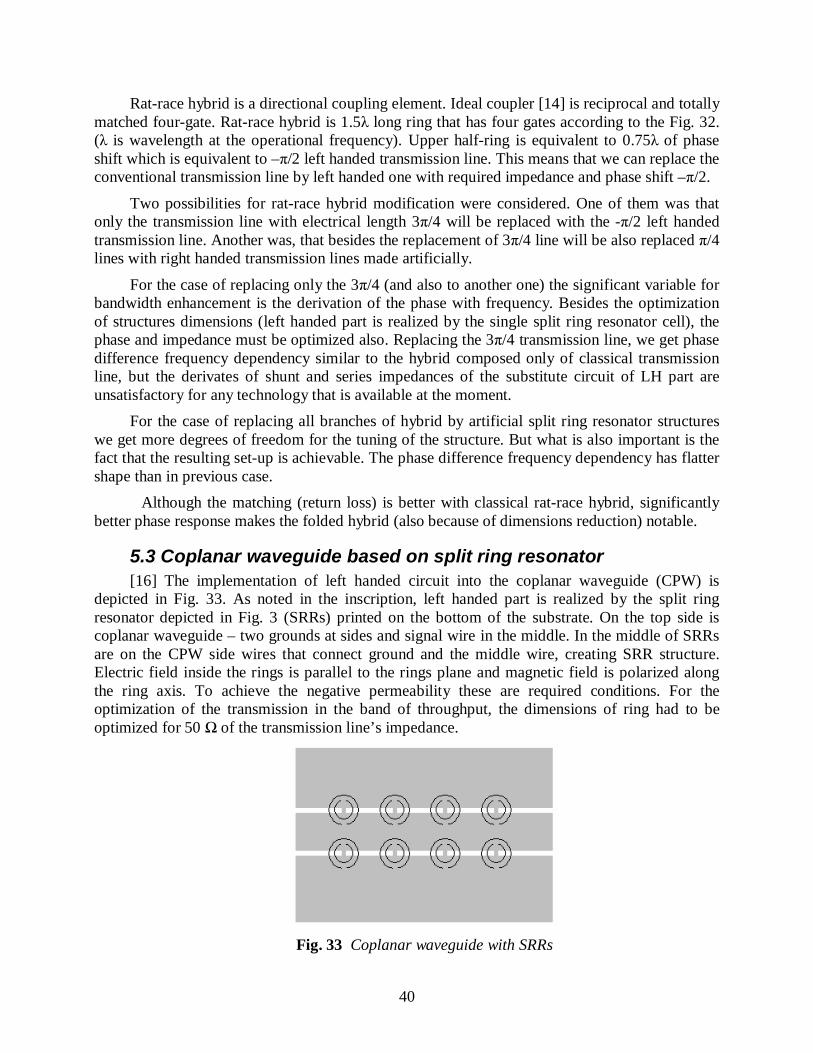
5.3 Coplanar waveguide based on split ring resonator [16] The implementation of left handed circuit into the coplanar waveguide (CPW) is
depicted in Fig. 33. As noted in the inscription, left handed part is realized by the split ring resonator depicted in Fig. 3 (SRRs) printed on the bottom of the substrate. On the top side is coplanar waveguide – two grounds at sides and signal wire in the middle. In the middle of SRRs are on the CPW side wires that connect ground and the middle wire, creating SRR structure. Electric field inside the rings is parallel to the rings plane and magnetic field is polarized along the ring axis. To achieve the negative permeability these are required conditions. For the optimization of the transmission in the band of throughput, the dimensions of ring had to be optimized for 50 Ω of the transmission line’s impedance.
Fig. 33 Coplanar waveguide with SRRs

41
For this structure is expected narrow band pass above the resonant frequency of SRR, where these conclusions are derived from the substitute circuit of the structure. The result of the simulation and measurement can be seen in Fig. 34. We can observe very narrow pass band just above the SRRs resonant frequency, what is very unusual for a planar structure, because normally they don’t achieve very high selectivity.
Fig. 34 Measurement (thick line) and simulation (thin line) results for the SRR CPW;
taken from [16]
Since negative material constants are available only in narrow band, the propagation of the signal is also reduced to this band. But the structure’s dimensions designate it for usage in miniature microwave circuits; along with good selectivity in the band pass. Moreover, if we remove the wires connecting signal and ground wire on the CPW side, we get stop band instead of band pass filter, thus we get another option for the design setup.
Besides electronics and communication, metamaterials have vast potential in many other fields, e.g. in optics – generating perfect lens [17], that don’t have the optical axis and can reproduce near field as good as far field with sub wavelength resolution employing so called plasmons (resonant surface waves).
Another field of use would be the radar absorbing material [18] – materials used before were afflicted by low durability and provided only limited range of angles and polarizations due to their anisotropy. Variety of computer techniques was used for the search of ideal absorbers (e.g. finite difference time domain method), but the advantage of metamaterials of controllable (to some extent) dispersion of permittivity and permeability make them good candidate for a new radar absorbing material.

42
6 Conclusion One of the aims of this work was to get acquainted with metamaterials, their properties and
what new do they bring to the world of modern science. This task is covered in chapters 1 to 3. One of the most important characteristics of metamaterial resonators is the possibility to govern the shape of the dispersion characteristic in certain range of frequencies (near resonance) what brings new dimensions to the microwave circuit design and engineering their parameters.
Another part of work is dedicated to design and simulation of the planar model of CRLH (Coupled Right Left Handed) transmission line. Parameters of the design were based on known values of capacitances and inductances of the substitute circuit. For this purpose Matlab functions were implemented for computation of dimensions of the lumped planar MIC (Microwave Integrated Circuit) employing the steepest descent method. Simulation of designed structures was done using Zeland’s IE3D simulation software, which was sufficient for our purpose.
Structures (first single-cell, then double-cell) were fabricated and measured. Comparing the measured and simulated traces gives reasonable consistency (values of resonant frequencies shift are between 1 and 3 %). This is potential for further work in this direction, simulated and measured were namely one and two cells in cascade, whereas source of our data presents results for four cascaded cells. The growing number of the structure’s cells causes the power loss increase, while the drift of resonant frequencies is not changing dramatically.
In the final part of this work are described various applications of metamaterials in radio engineering and not only there. This relatively young object of research is still not fully examined, although the idea of negative refraction media is known for more than forty years. Because of this fact, there is a lot of space for further research in many sectors of industry and science.

43
References [1] GUPTA, K. C., GARG, R., BAHL, I., BHARTIA, P. Microstrip lines and slot lines. 2nd
ed. Norwood: Artech House, 1996. [2] HOFFMANN, K. Planar microwave circuits (in Czech language). Skriptum FEL ČVUT.
Praha: Vydavatelství ČVUT, 2000. [3] HONG, J. S., LANCASTER, M. J. Microstrip Filters for RF/Microwave Applications. New
York: J. Wiley and Sons, 2001. [4] KAMALJEET, S., DEEPANKAR, R., RAMSUBRAMANIAN, R. Microstrip Filters
Provide High Harmonic Suppression [online]. Available from WWW: <http://www.highbeam.com/Microwaves+~A~+RF/publications.aspx?pageNumber=1&date=200604>. Apr 01, 2006
[5] ENGHETA, N. An idea for thin sub-wavelength cavity resonators using meta-materials with negative permittivity and permeability. IEEE Antennas and Wireless Propagation Letters. 2002, vol. 1, no. 1, p. 10–13.
[6] ALLEN, C.A., LEONG, K., ITOH, T. Design of microstrip resonators using balanced and unbalanced composite right/left-handed transmission lines. IEEE Transactions on Microwave Theory and Techniques. 2006, vol. 54, no. 7, p. 3104 to 3112.
[7] PENDRY, J.B., SMITH D.R. Looking for super-lens (in Czech language). Scientific American, March-April 2007, p. 96-103.
[8] MATHWORLD, Method of steepest descent [online]. Available from WWW: <http://mathworld.wolfram.com/MethodofSteepestDescent.html>.
[9] DĚDKOVÁ, J. Modelování elektromagnetických polí, přednášky. Electronic scriptum FEKT Vysokého učení technického v Brně
[10] ECHO MICRO SYSTEMS, IE3D features [online]. Available from WWW: < http://www.echoms.co.kr/html/prod/feature.html >
[11] ANSOFT CORPORATION, Left-Handed Metamaterial Design Guide [online]. Available from WWW: <http://www.ansoft.com/metamaterial/>.
[12] BILKENT UNIVERSITY, Labyrinth based left handed metamaterials [online]. Available from WWW: <http://www.nanotechnology.bilkent.edu.tr/left-handed-transmission.htm >.
[13] BILKENT UNIVERSITY, Negative refraction and sub-wavelength focusing using composite metamaterials [online]. Available from WWW: <http://www.nanotechnology.bilkent.edu.tr/negative-refraction.htm>.
[14] SVAČINA, J., Hybridní členy v MIT [Power Point presentation]. Brno: FEEC BUT in Brno, 2008
[15] SISÓ, G., GIL, M., BONACHE, J., MARTÍN, F. Applications of resonatnt-type metamaterial transmission lines to the design of enhanced bandwidth components with compact dimensions [online]. Available from WWW: <http://www3.interscience.wiley.com/journal/116845152/abstract >.

44
[16] MARTÍN, F., BONACHE, J., FALCONE, F., SOROLLA, M., MARQUÉS, R. Split ring resonator-based left-handed coplanar waveguide [online]. Available from WWW: <http://www.personal.us.es/marques/SRR-based-LH-CPW.pdf>
[17] FAUSTUS SCIENTIFIC CORPORATION. An Almost Perfect Lens [online]. Available from WWW: <http://www.faustcorp.com/products/mefisto3dpro/metamaterials/slide07.html>
[18] PACHECO, J. Theory and Application of Left-Handed Metamaterials: Candidate disertation. Massachusetts Intstitute of Technology, 2004. 235 p.
[19] Wikipedia – online thesaurus [online]. Avialable from WWW: <http:// en.wikipedia.org/>.

45
List of acronyms and symbols AIF Advanced Intelli Fit CMM Composed Metamaterial CPW Coplanar Waveguide CRLH Coupled Right-Left Handed CSRR Closed Split Ring Resonator EM Electro-Magnetic LH Left Handed MIC Microwave Integrated Circuit RH Right Handed SRR Split Ring Resonator TL Transmission Line
A1, A2 Coeficients used for calculation of parameters of interdigitall capacitor β(f) Frequency dependent phase constant β Attenuation constant c Light velocity C Capacitance d Thickness Exn Electric field component ε0 Permittivity of vacuum εr Relative permittivity of dielectric εef Effective permittivity of dielectric
i∋ Length of the step fR Resonant frequency h Substrate height Hyn Magnetic field component k Wave number l Length L Inductance λ0 Free space wavelength λg Wavelength in TL n Refracion index N Number of cells μ0 Permeability of vacuum μR Relative permeability ω Angular frequency Q Quality factor r Radius RS Serial resistance RSS Specific high-frequency resistance S1, S2 Poyinting vectors s11 Scattering parameter – input reflection s22 Scattering parameter – output reflection

46
s21 Scattering parameter – transmission t Metalization thickness v, vg, vp Wave’s velocity – in free space, group velocity, phase velocity w Microstrip width σC Conductivity θ Incidence angle Δ Variation Zv Wave impedance ZL Impedance of a shunt inductor

47
List of appendices 1 Matlab source code 2 Measured cell dimensions

48
Appendix 1 – Matlab source code Iteration loop for calculation of capacitance of inter-digital capacitor: for n=1:N E1 = (CC-Cg3( s, w, h, er, l+del, n))^2 - (CC-Cg3( s, w, h, er, l-del, n))^2; E3 = (CC-Cg3( s+del, w, h, er, l, n))^2 - (CC-Cg3( s-del, w, h, er, l, n))^2; l = l - alp*E1/del; s = s - alp*E3/del; if h/x<3 x = h/3; end if h/x>1e3 x = 3*h; end Cx(n) = Cg3(s, w, h, er, l, n); end
Here CC is desired value of capacitance and function Cg3 calculates actual capacitance value from input parameters and is changing according to the variation of l – length of finger and s – gap width. From difference between desired and actual value are calculated error functions E1 and E3, which are used for length and gap width correction. Values of capacitance are stored into the vector Cx, which allows us to observe the history of capacitance values through iteration loop. Conditions for h/x, where x = s (and h is substrate height) relation are prevention from divergence of gap width – s.
The output of iteration loop is capacitance Cx at the end of the loop (see Fig. 36), length of fingers – l and gap width – s. After N = 20 iteration steps, parameters obtained were: Cx = 0.3130 pF (desired was 0.32), l = 15.3 mm and s = 2.3 mm.
Fig. 36 Capacitance iteration graph
Similar iteration loop was used for calculation of parameters of shunt inductor, output for this iteration after 40 steps was length of inductor – l = 24.18 mm and its inductance – L = 0.1629 nH (desired 0.16 nH).

49
Appendix 2 – One cell structure dimensions In the figures below are depicted single cell structures with coted dimensions. The cell
tuned at 6 GHz is obviously symetricall, but the one tuned at 6.5 GHz not.
Dimensions of a single cell tuned at 6 GHz in mm
Dimensions of a single cell tuned at 6.5 GHz in mm