< GCT(Gate Commutated Turn-off) Thyristor Unit > GCU04BB-130
MODELLING AND SWITCHING SIMULATION OF GATE TURN-OFF THYRISTOR USING FINITE ELEMENT METHOD
NORAINON MOHAMED
Thesis submitted in fulfilment of-the requirements for the award of the degree of Master of Engineering in Electrical
Faculty of Electrical and Electronics Engineering IJNIVERSITI MALAYSIA PAHANG
MAY 2010
ABSTRACT
The gate turn-off (GTO) thyristor has the best voltage blocking and current conducting
capabilities among all known high power semiconductor switching devices. The
switching characteristics of a GTO thyristor are influenced by doping profile, material
properties, lifetime and mobility of holes and electrons. Recently, most of the research
on GTO thyristor is strictly experimental and has focused on their physical
performances. On the other hand, the internal behaviour of GTO thyristor is not well
understood. The best accuracy switching waveforms and the internal behaviour of the
device can only be addressed by device simulation. Physical models (Poisson equation,
drift-diffusion and current-continuity equations) of GTO thyristor are valuable for
studying the internal behaviour of the device is used in the simulation. These equations
are numerically solved by using finite element method. This project presents: the
modelling and switching simulation of GTO thyristor device by developing a device
simulation software. The software is designed by using MATLAB Graphical User
Interface (GUI) development environment. The device model has been developed based
on the device structure and operation. The thesis focuses on the study of a comparison
between silicon and silicon carbide GTO thyristor in terms of switching time
performances and efficiency at the system level.
vii
ABSTRAK
Gate turn-off (GTO) thyristor mempunyai voltan sekatan terbaik dan kemampuan arus
pengaliran di antara peranti-peranti pensuisan separa pengalir berkuasa tinggi. Ciri-ciri
pensuisan sebuah GTO thyristor dipengaruhi oleh profil doping, sifat-sifat bahan,
jangkahayat dan mobility lubang-lubang dan elektron-elektron. Baru-baru mi,
sebahagian besar penyelidikan tentang GTO thyristor adalah terhad kepada ujikaji dan
hanya tertumpu kepada persembahan fizikal sahaja. Sebaliknya, perilaku dalaman GTO
thyristor tidak difahami dengan baik. Ketepatan terbaik gelombang pensuisan dan
perilaku dalaman peranti hanya boleh ditangani melalui simulasi peranti. Model-model
fizikal (persamaan Poisson, persamaan-persaman hanyutan-resapan dan
kesinambungan-arus) GTO thyristor adalah sangat berharga untuk mempelajari perilaku
dalaman peranti digunakan dalam simulasi. Persamaan secara berangka diselesaikan
dengan menggunakan kaedah elemen terhingga. Projek mi mempersembahkan
permodelan dan simulasi pensuisan GTO thyristor dengan membangunkan satu perisian
simulasi. Perisian mi direka dengan menggunakan MATLAB Antara Muka Grafik
(GUI) persekitaran pembangunan. Model peranti telah dibangunkan berdasarkan
struktur peranti dan operasi peranti. Tesis mi memfokuskan kepada penyelidikan antara
silicon dan silicon carbide GTO thyristor dari segi perbandingan antara prestasi
pensuisan dan kecekapan di peringkat sistem.
viii
TABLE OF CONTENTS
Page
EXAMINERS APPROVAL DOCUMENT
SUPERVISOR'S DECLARATION
STUDENT'S DECLARATION iv
DEDICATION
ACKNOWLEDGEMENTS vi
ABSTRACT vii
ABSTRAK viii
TABLE OF CONTENTS ix
LIST OF TABLES xii
LIST OF FIGURES xili
LIST OF SYMBOLS xv
LIST OF ABBREVIATIONS xvii
CHAPTER 1 INTRODUCTION
1.1 Background 1
1.2 Problem To Be Addressed 3
1.3 Research Approach 5
1.4 Research Objectives 6
1.4.1 Physical Characteristics of Si and SiC 7 • 1.4.2 Switching Characteristics of Si GTO and SiC GTO Thyristors 7
1.4.3 Development of GTO Thyristor Simulation Tool 7
1.5 Research Scopes 8
1.6 Thesis Organization 9
lx
x
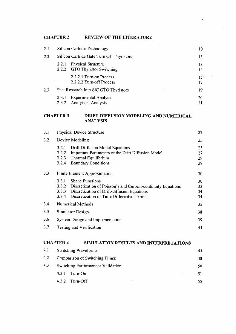
CHAPTER 2 REVIEW OF THE LITERATURE
2.1 Silicon Carbide Technology 10
2.2 Silicon Carbide Gate Turn Off Thyristors 13
2.2.1 Physical Structure 13 2.2.2 GTO Thyristor Switching 15
2.2.2.1 Turn-on Process 15 2.2.2.2 Turn-off Process 17
2.3 Past Research Into SiC GTO Thyristors 19
2.3.1 Experimental Analysis 20 2.3.2 Analytical Analysis 21
CHAPTER 3 DRIFT-DIFFUSION MODELING AND NUMERICAL ANALYSIS
3.1 Physical Device Structure 22
3.2 Device Modeling 25
3.2.1 Drift Diffusion Model Equations 25 3.2.2 Important Parameters of the Drift Diffusion Model 27 3.2.3 Thermal Equilibrium 29 3.2.4 Boundary Conditions 29
3.3 Finite Element Approximation 30
3.3.1 Shape Functions 30 3.3.2 Discretization of Poisson's and Current-continuity Equations 32 3.3.3 Discretization of Drift-diffusion Equations 34 3.3.4 Discretization of Time Differential Terms 34
3.4 Numerical Methods 35
3.5 Simulator Design 38
3.6 System Design and Implementation 39
3.7 Testing and Verification 43
CHAPTER 4 SIMULATION RESULTS AND INTERPRETATIONS
4.1 Switching Waveforms
4.2 Comparison of Switching Times 48
4.3 Switching Performances Validation 50
4.3.1 Turn-On 51
4.3.2 Turn-Off

xl
4.4 Inner Phenomena 59
CHAPTER 5 CONCLUSION AND FUTURE WORK SUGGESTIONS
5.1 Conclusion 63
5.2 Future Work Suggestions 64
5.2.1 Device Structure Modification 64 5.2.2 Numerical Stability of the Simulations 65 5.2.3 Testing and Verification 65
REFERENCES 67
APPENDICES
A GTO Thyristor Doping Data 75
B Si and SiC GTO Thyristor Switching Data 86
C Pseudo-code Listing 104
D List of Publications 105
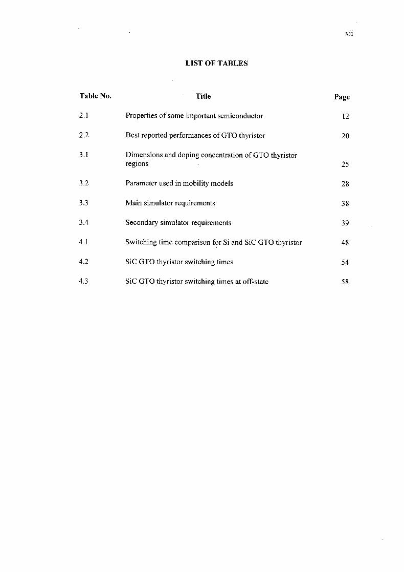
LIST OF TABLES
Table No. Title Page
2.1 Properties of some important semiconductor 12
2.2 Best reported performances of GTO thyristor 20
3.1 Dimensions and doping concentration of GTO thyristor regions 25
3.2 Parameter used in mobility models 28
3.3 Main simulator requirements 38
3.4 Secondary simulator requirements 39
4.1 Switching time comparison for Si and SiC GTO thyristor 48
4.2 SiC GTO thyristor switching times 54
4.3 SiC GTO thyristor switching times at off-state 58
xli
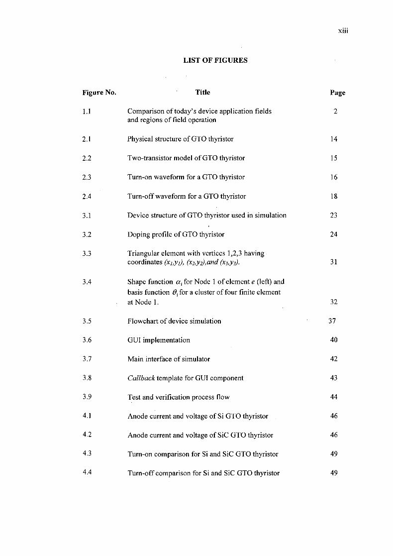
LIST OF FIGURES
Figure No. Title Page
1.1 Comparison of today's device application fields 2 and regions of field operation
2.1 Physical structure of GTO thyristor 14
2.2 Two-transistor model of GTO thyristor 15
2.3 Turn-on waveform for a GTO thyristor 16
2.4 Turn-off waveform for a GTO thyristor 18
3.1 Device structure of GTO thyristor used in simulation 23
3.2 Doping profile of GTO thyristor 24
3.3 Triangular element with vertices 1,2,3 having. coordinates (xj,yj), (x2,y2),and (x3,y3). 31
3.4 Shape function a 1 for Node 1 of element e (left) and
basis function O for a cluster of four finite element at Node l. 32
3.5 Flowchart of device simulation 37
3.6 GUI implementation 40
3.7 Main interface of simulator 42
3.8 Callback template for GUI component 43
3.9 Test and verification process flow 44
4.1 Anode current and voltage of Si GTO thyristor 46
4.2 Anode current and voltage of SiC GTO thyristor 46
4.3 Turn-on comparison for Si and SiC GTO thyristor 49
4.4 Turn-off comparison for Si and SiC GTO thyristor 49
xlii
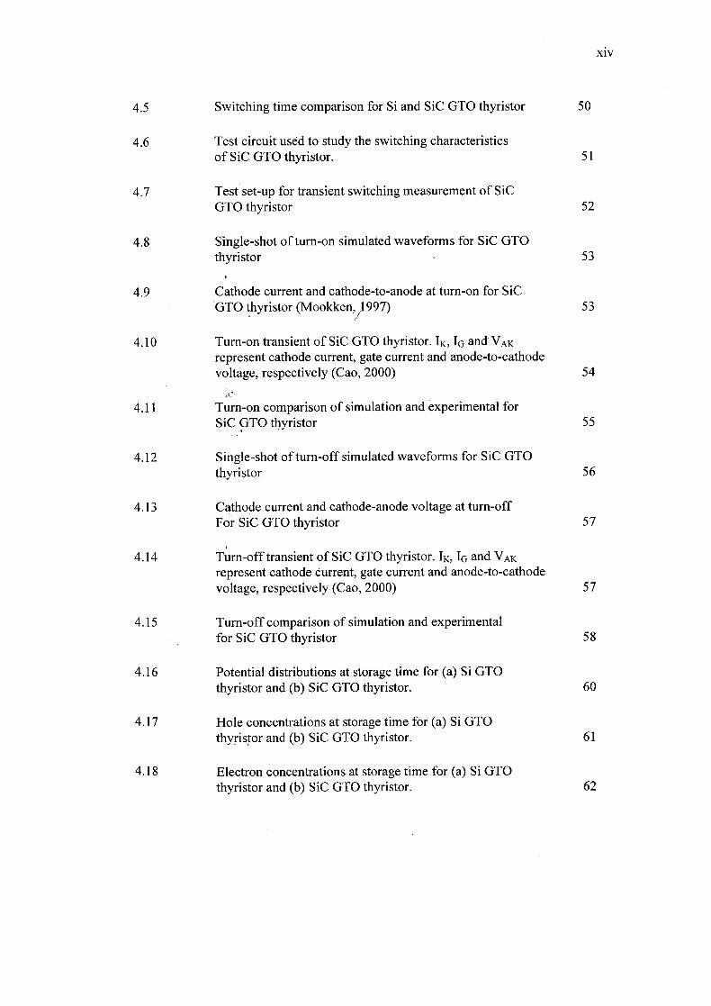
4.5 Switching time comparison for Si and SiC GTO thyristor
4.6 Test circuit used to study the switching characteristics of SiC GTO thyristor.
4.7 Test set-up for transient switching measurement of SiC GTO thyristor
4.8 Single-shot of turn-on simulated waveforms for SiC GTO thyristor
4.9 Cathode current and cathode-to-anode at turn-on for SiC GTO thyristor (Mookken /1 997)
4.10 Turn-on transient of SiC GTO thyristor. 'K, 'G and VAK
represent cathode current, gate current and anode-to-cathode voltage, respectively (Cao, 2000)
4.11 Turn-on comparison of simulation and experimental for SiC GTO thyristor
4.12 Single-shot of turn-off simulated waveforms for SiC GTO thyristor
50
51
52
53
53
54
55
56
xiv
4.13 Cathode current and cathode-anode voltage at turn-off For SiC GTO thyristor
4.14 Turn-off transient of SiC GTO thyristor. 'K, JG and VAK
represent cathode current, gate current and anode-to-cathode voltage, respectively (Cao, 2000)
4.15 Turn-off comparison of simulation and experimental for SiC GTO thyristor
4.16 Potential distributions at storage time for (a) Si GTO thyristor and (b) SiC GTO thyristor.
4.17 Hole concentrations at storage time for (a) Si GTO thyristor and (b) SiC GTO thyristor.
4.18 Electron concentrations at storage time for (a) Si GTO thyristor and (b) SiC GTO thyristor.
UN
WA
58
61
62
LIST OF SYMBOLS
kB Boltzmann's coefficient
a Curve fitting parameter
Nd Doping profile
n Electron
Electron acceptor concentration
vfl Electron carrier lifetime
Electron density
D Electron diffusion constant
Electron donor concentration
Pn Electron mobility
çb Electron quasi Fermi level
Electrostatic potential
q Elementary charge
P Hole
V P Hole carrier lifetime
Hole density
D Hole diffusion constant
xv
11,. Hole mobility

xvi
Op Hole quasi Fermi level
Anax Maximum mobility
Pmin Minimum mobility
P Mobility
e Permittivity coefficient,
R Recombination rate
Nref Reference concentration
T Temperature
n i Intrinsic carrier concentration

LIST OF ABBREVIATIONS
2D two-dimensional
3D three-dimensional
FEM Finite element method
GTO Gate turn-off
GUI Graphical user interface
GUIDE Graphical user interface development environment
MATLAB Matrix Laboratory
OS Operating system
SCRs Silicon controlled rectifiers
Si Silicon
sic Silicon Carbide
SRH Shockley-Read-Hall
XVII
CHAPTER 1
INTRODUCTION
1.1. BACKGROUND
Power devices are essential components of most electronics devices and
systems which used to control the energy transfer of electronics systems.
Recently, due to the growing of global interest in energy saving, efficiency is
becoming more important in power devices. Therefore, it is very important to
develop power devices that have lower loss and higher efficiency.
Power devices are also required to operate over a broad spectrum power
level and frequencies (Tolbert et. al, 2005). As shown in Figure 1.1, passage to
power levels of up to 10MW still depends on the development of high-voltage
gate-turn off (GTO) thyristors (Gorbatyuk, 2008). Being a device in thyristor
family, GTO is making a significant impact in power electronics design. A GTO
has the best voltage blocking and high current conducting capabilities among all
known high power devices. The ability to turn off the current without reversal of
the anode to cathode voltage (Cooper and Agarwal, 2002) has evolved new
circuits concepts such as self-commutated, pulse-width modulated (PWM),
voltage-driven and multi-step converters, and enables the circuits to operate at
higher frequency.
Almost all power devices are fabricated using Silicon (Si), but their
performances have approached theoretical limits of Si power devices. Si power
devices are limited to operation of low switching speed and low blocking
voltages by virtue of the physical properties of Si. Hence, in high power

2
applications, which require efficient, the use of Si is restricted. It is necessary to
put semiconductors haying better properties than Si in practical use. Much of the
research efforts is aimed at developing new semiconductor technologies (Silicon
Carbide and Gallium Nitride for example) to improve the existing Si technology.
At the moment, silicon carbide (SiC) is one of the candidates for the
semiconductor technology for innovative power devices that will replace Si
devices (Tamaso, 2008). Compared to current power devices made of Si, SiC
have wide bandgap, low intrinsic carrier concentration, and high thermal
conductivity make it suitable for high-voltage and high-power density
applications (Muzykov, 2009).
Power Transmission UPS, Industrial Inverter 100 M- - -------------
________________ Motor Dives lOM - 1' L/"-2T-------- -f
Robot Welding Machines I M GTO
100k— . THYRISTOR
10k—I .
1k]
100
10
----------Switchingpower supply
Home appliances, Computer, Digital products
10 100 1 k 10k 100k 1 M
Frequency (Hz)
Figure 1.1: Comparison of today's devices application fields and regions of
operation.
GTO thyristors with this new semiconductor technology has been
experimentally and numerically demonstrated by researchers with different
applications. Experimentally, researchers have demonstrated SiC GTO thyristors
as the switching devices in circuits driving resistive and inductive loads (Bayne,

3
2002; Agarwal, 2001; Ryu, 2001). However, internal behaviour of the devices
was not examined in-deth. At present, most of the research into SiC GTO
thyristors has focused on high forward blocking voltages, but with low forward
currents (Bayne, 2002; Cao, 2000). They were not able to produce both high
forward blocking voltages and high-on currents on the same device.
In order to analyze the working of the device, a mathematical. model is
developed to describe the device. While developing the mathematical model,
some assumptions are made for simplification. Finally, the governing
mathematical expression is developed to describe the behaviour of the device.
The mathematical expression usually consists of differential equations and given
conditions. These differential equations are usually very difficult to obtain
solutions which explain the behaviour of the given circuit system. With the
advent of high performance computers, it has become possible to solve such
differential equations.
Various numerical solution techniques have been developed and applied
to solve numerous engineering problems in order to find their apprOximate
solutions. Especially, the finite element method (FEM) has been one of the
major numerical solutions. In particular, any complex shape of problem domain
with prescribed conditions can be handled with ease of FEM. The most
significant practical advantage is the ability to handle solution domains with
arbitrary geometry (Pozrikidis, 2005).
1.2. PROBLEM TO BE ADDRESSED
At present, much of the research being performed with SiC GTO
thyristor is strictly experimental (Bayne, 2002; Tripton et. al, 2002; Ryu et. al,
2001) - the device is fabricated, placed into test circuits, and operated until
either the tests are completed successful or the device fail. Unfortunately, these
experiments can take a significant amount of time and money to set up and they
usually do not lend themselves to directly examining what happens within the
internal structure of the device. Thus, it can be difficult to determine exactly how

a device operates (or fails to operate) through experimentation. At this point,
correction has to be made. They can be done by using an appropriate simulation
tool. Experimental techniques can do this only approximately and for a few
parameters.
Most of the research into SiC GTO thyristor and their limitations have
focused on several voltage and current ratings (Yurkov et. al. 2005). Although
this device demonstrated reasonable forward blocking voltages, they were not
able to produce both high forward blocking voltages and high-on currents on the
same device due to its limitations in device fabrication. The results of previous
research are only shows for certain amount of voltage which can be applied to
the device, otherwise the device would have high losses and less efficient.
Studying performance of power devices, need to visualise the working of
devices in a way can be addressed by device simulation. But, professional-level
simulators are not particularly accessible in instructional context They were
only available to relatively large commercial engineering concerns. These
simulation tools were extremely expensive and in many cases required a large
amount of equally training to make effective to use of them. Therefore, a modern
simulation tool which more "user-friendly" and ease-to-use need to be
developed. The simulation tool also allows you to get up and operational without
needing several days or working of training on how to use the tool. However, the
tool still requires some fundamental understandings of what you are working
with.
A physics-based simulation tool would allow researchers to evaluate
semiconductor devices, both new and existing technologies, with less physical
experimentation. The researchers would be able to evaluate "what-if' scenario
rapidly and see which devices merit further study and which devices require
additional design effort. The simulation would also provide full-field and in-
depth understanding and show what happen inside the semiconductor devices,
which allow the researchers to understand exactly how the devices operate and
how they are likely to fail.
1.3. RESEARCH APPROACH
This research utilized the semiconductor physical models of a GTO
thyristor and simulates its operation in a circuit test circuit by developing a
simulation tool with Si and SiC as the semiconductor materials. The simulation
tool was developed to perform physics-based of the GTO thyristor. The primary
software used to develop the simulation tool was MATLAB Graphical User
Interface Development Environment (GUIDE). GUIDE, the MATLAB GUI
development provides a set of tools for creating GUIs. These tools simplify the
process of laying out and programming GUIs.
The first phase of this research consisted of developing behaviour and
circuit models of a GTO thyristor by using semiconductor transport equations.
The equations describe the static and dynamic behaviour of carriers in
semiconductors under the influence of external fields that cause deviation from
the thermal equilibrium conditions. The equations to be used in the research are
as follows: current-continuity equations, Poisson equation, and drift-diffusion
equations. Finite element method (FEM) will be implemented in order to solve
these equations. This method numerically approximates the solution of the
equations by replacing the continuous system with a finite number of non-linear
algebraic equations. Final forms of these equations will be used for developing
simulation tool by using MATLAB GUI development environment.
The second phase of the research are testing and validating the software.
Switching performances of GTO thyristor were validated using a set of voltage
and current waveforms that were collected during a previous experimental study
of GTO thyristor with SiC semiconductor material (Mookken, 1997). In the
switching waveforms validation phase, the circuit condition in the simulation
was adjusted to match the switching waveforms of the simulated GTO thyristor
to match the experimentally switching waveforms. The validation phase was
also used to compare the switching time of the previous experimental study in a
circuit operation.
The third and the final phase of the research, the simulation results were
used to investigate the switching characteristics of Si and SiC GTO thyristor.

The investigation includes the turn-on and turn-off time and comparison of the
performances for both Si and SiC. The simulation results were also used to
investigate the inner phenomena of GTO thyristor for both Si and SiC. This step
is further verified the switching characteristics of GTO thyristor by correctly
simulating the device internal behaviour or inner phenomena of potential, holes
and electron distributions during switching time that have been shown in
previous GTO thyristor research with SiC material (Shah, 2000). For this part of
research project, the simulation file for the physical structure was fixed at each
transient time. Each doping layer file of GTO thyristor stored the solutions to the
physical models (Poisson's equation, current-continuity equations and drift-
diffusion equations) at each point of a specific transient time. This data
(potential, holes and electron distributions) was used to investigate the electrical
characteristics of GTO thyristor during its switching operation in a circuit.
1.4. RESEARCH OBJECTIVES
The overall goal of this research project is to investigate the switching
performances of GTO thyristor. The switching performances should be able to
explain, extract and predict the operation of GTO thyristor for variety input gate
and anode voltages. The objectives have been divided into three distinct parts -
physical characteristics of Si and SiC, switching characteristics of GTO thyristor
and development of simulation tool for GTO thyristor.
1.4.1. Physical characteristics of Si and SiC
Physical characteristics for both materials will be investigated through
physical models which consisted of semiconductor equations. From the
equations, .physical characteristics can be modelled by using finite element
method. These method is numerically approximate the solution of the
semiconductor equations by replacing the continuous system with a finite
number coupled linear algebraic equations. The linear algebraic equations used
to describe the behaviour of Si and SiC in GTO thyristor lumped with non-linear
element into a test circuit.

7
1.4.2. Switching characteristics of Si GTO and SiC GTO thyristors
Switching characteristics of Si GTO and SiC GTO thyristors will be
analyzed in terms of turn-on and turn-off processes. During turn-on and turn-off
processes, Si GTO and SiC GTO thyristors are subjected to different voltages
across it and different currents through it. The time variations of the voltage
across Si GTO and SiC GTO thyristors and the current through them during
turn-on and turn-off processes give the dynamic or switching characteristics of
Si GTO and SiC GTO thyristors. Here, switching characteristics during turn-on
are described and then the switching characteristics during turn-off. Switching
time comparison for both Si GTO and SiC GTO thyristor will be explained in-
depth.
1.4.3. Development of GTO thyristor simulation tool
The simulation tool to be developed incorporates the device physical
models such as Poisson, current-continuity and drift-diffusion equations. Its
basic function enables user to investigate GTO switching performances and
inner phenomena (potential, hole and electron concentrations) through circuit
modification and characteristic observation. Simulation results shall confirm to
theoretical and experimental analysis of the device. Besides allowing the user to
investigate the device performance, the software will also allow for relatively
easy inclusion of the new semiconductor material (SiC). Relatively easy means
it can be done by selecting new materials (Si or SiC) and modify the circuit
condition to see the effect of the chosen material in terms of switching speed. To
facilitate ease of use, the simulator will have a Graphical User Interface (GUI).
1.5. RESEARCH SCOPES
This research will introduce a new physical model of SiC. The
investigation of switching performances (turn-on and turn-off) of Si and SiC
GTO thyristors will be visualized into two-dimensional (213) and three-
dimensional (313) plots, through the simulation results including the phenomena
inside the device. The physical models has been chosen for GTO thyristor are
8
i) Poisson's equation
ii) Drift-diffusion equations
iii) Current-continuity equations
To achieve all the research's objectives, knowledge in the following
information in necessary
i) Finite element method implementation into the physical models.
ii) Major physical models: drift-diffusion and current-continuity
equations, generation-recombination model, mobility model.
iii) Si and SiC physical properties: electron and hole mobility, ionization
coefficients, lifetime, intrinsic semiconductor density.
iv) High-level software and development tool: MATLAB Graphical
User Interface Development Environment (GUIDE).
1.6. THESIS ORGANIZATION
The remaining chapters of this thesis are organized as follows:
Chapter 2 presents the details of electrical properties and physical
characteristics of SiC. GTO thyristor structure and switching characteristics will
be discussed briefly. This chapter also discussed the past research of SiC GTO
thyristor that provided the foundation for this thesis.
Chapter 3 describes the GTO thyristor structure which to be used in this
research project. The semiconductor and drift-diffusion equations to be used in
simulation, and the implementation of finite element method in the equations
also will be explained in details. This chapter describes the discretization of the
equations by using finite element method. Software development approaches,
methods taken to validate the results and also discussion on how to implement
the equations into programming language will be explained in this chapter.
Chapter 4 presents the discussions on the simulation results. Data from
the simulation will be visualized into two-dimensional (2D) and three-
dimensional (313). The results will be presented into a list of data and graph.
This chapter also discussed the switching characteristics during turn-on and turn-
off states and comparison for both Si and SiC GTO thyristor will be discussed,
and inner phenomena of the device will be visualized through three-dimeional
plots. Testing and validation of the results shall confirm the theoretical and
experimental data from previous work which has been described in Chapter 2.
Chapter 5 will summarize the whole thesis and give out some
suggestions on future work. The simulation related information and source code
listing of the simulator are attached in appendices.
CHAPTER 2
REVIEW OF THE LITERATURE
Before analyzing the switching performances GTO thyristor made from
SiC, it is important to know about SiC properties and the device benefits of these
properties. In this chapter, an introduction about SiC material will be presented
followed by its advantages to the GTO thyristors in terms of switching
performances. Past research of GTO thyristors with this material will be
discussed in the next section.
2.1. SILICON CARBIDE TECHNOLOGY
An ideal power device should exhibit the following features: carrying
any amount of current with zero on-state voltage drop in forward conduction
mode, holding off any value of voltage with zero leakage current in the blocking
mode, and switching between the on-state and off-state with zero switching time
(Elasser, 2002). Practical power devices, however, always exhibit a finite
resistance when carrying current in the on-state as well as finite leakage current
while operating in the off-state under certain breakdown voltage, both of which
lead to power switch (Elasser, 2002). Hence, in reality, the research work on
power devices on utilizing advanced materials as well as innovative device
structures, or processing techniques to improve the on-resistance, blocking
capability and switching time.
Si power devices have served the industry over a long time and they
currently, dominate power electronics market. Due to inherent limitations of Si
material properties, such as narrow bandgap, low thermal conductivity and low

I
breakdown voltage, Si power devices are approaching theoretical limits in terms
of higher power and higher temperature operations, offering no significant
improvement in device performances with further investment (Chintavali, 2003).
With the development of high quality substrates and processing
technologies, 4H-SiC power devices are expected to outperform their Si
counterparts in high-power and 'high-temperature applications, due to the
inherent material advantages of 4H-SiC. The material properties of 4H-SiC are
listed and compared with other important semiconductor materials in Table 2.1 1
(Wu, 2009). In comparison to Si, 4H-SiC has the following advantages:
v' The breakdown field is 10 times as high as that Si. For the same voltage
rating, 4H-SiC devices can be designed using a much thinner drift region and
higher drift doping than that required for their Si counterparts. Thus the
specific on-resistance could be significantly reduced, resulting in the much
lower conduction power loss and improved power efficiency.
V As a wide bandgap material, 4H-SiC has a bandgap 3 times as wide as that
of Si, which means the current increase due to thermal generation is much
lower than Si. In other words, the intrinsic temperature, at which the intrinsic
carrier concentration becomes comparable to the doping concentration, is
extremely high for SiC devices. Hence, SiC power devices are capable to
operate at much higher temperatures, enabling compact power systems with
reduced cooling needs. In addition, the wide bandgap of 4H-SiC keeps its
power devices from the degradation of electronic properties under high
radiation environment such as aerospace.
The electron saturation velocity of 4H-SiC is two times than Si. During the
switching of diode, the higher electron saturation velocity of 4H-SiC can
offer shorter reverse recovery time, as charge stored in the depletion region
can be removed faster. Hence, 4H-SiC power devices can be switched at
higher frequencies then their Si counterparts.
" Thermal conductivity of 4H-SiC is three times as high as that Si. As an
excellent thermal conductor, 4H-SiC power devices has stronger thermal
12
stability, allowing that heat generated in the power devices to be transmitted
to a heatsink and the ambient more easily.
Among the wide bandgap semiconductor materials, SiC materials are by
far the most developed for power devices in terms of substrate quality and
device processing. According to Table 2.1, diamond is theoretically the best
candidate for power devices as it has the highest electric breakdown field, the
largest bandgap and the highest thermal conductivity (Wu, 2009). However, its
material quality and device fabrication technology are still in its infancy.
Table 2.1 Properties of some important semiconductor.
Wide Bandgap Semiconductors
Materials Si_ GaAs GaN 3H SiC 4H-SiC 61-1 SiC Diamond Bandgap Eg
1.4 3.39 2.2 3.26 3 5.45 (eV) Intrinsic
Concentration, n, (CM-3) 1.5xl0'0 1.8x10⁶ 1.9x10¹⁰ 6.9 8.210 2.3x10 6 1.6x1027
Dielectric11:8 12.8 9 9.6 10 9.7 5.5
Constant, Er
Electron Mobility 2 u_(cm _/V-S)
1350 8500 900 900 1148 0// 370//c 1900
Breakdown
Field, E 0.3 0.4 3.3 1.2 3 2.4 5.6 (MV/cm)
Electron Mobility Saturation Velocity 1 2 2.5 2 2 2 2.7
V(l0_cm/s Thermal
Conductivity k 1.5.1 0.5 1.3 4.9 4.9 4.9 20 (W/cm-K)
Direct/Indirect Indirect Direct Direct Indirect Indirect Indirect
___
Indirect
SiC occurs in more than 170 polytypes (which are different crystal
structures with the same stoichiometry of a compound semiconductor). Only the
13
6H-SiC and 4H-SiC polytypes are available commercially in both bulk wafers
and custom epitaxial layers (Elasser, 2002). The most suitable and established
SiC polytype for high temperature power electronics is the hexagonal 4H
polytype (Willander, 2006) and has been chosen in the research because of its
high carrier mobility and its low dopant ionization energy.
2.2. SILICON CARBIDE GATE TURN OFF THYRISTORS
Gate Turn Off thyristors (commonly referred to simply as GTOs) are
solid state device semiconductor switches that are designed for high power
switching applications. To date, the GTO thyristor has the highest power rating
and the best trade-off between the blocking voltage and the conduction loss of
any fully controllable switch. The main advantage over the thyristor is the higher
switching speed and the ability to turn off the current without reversal of the
anode to cathode voltage (Cooper and Agarwal, 2000).
2.2.1. Physical Structure
Physically, GTO thyristor is a power semiconductor device with three
junctions and three terminals, has a four-layered structure that consists of
multiple unit cells connected together in parallel. Each unit cell is comprised of
alternating layers of n-type and p-type semiconductor material. In many GTO
thyristor, the anode electrode is shorted directly to the wide n-base region as
shown in Figure 2.1; the anode shorts are typically added to improve the GTO
thyristor's turn-off properties (Vineyard, 2009). Anode shorts are incorporated
to provide a path for electrons to reach the contact metallisation, without the
injection of holes (Galster, 2007). This type of thyristor is suitable for
applications that require high-speed switching, but do not need high reverse
voltage.
The four-layer structure of a GTO thyristor. allows each unit cell to
operate like a pair of coupled bipolar junction transistors as shown in Figure 2.2
(Chintavali, 2003). In the off-state, the wide n-base region is able to support a

Gate
14
large depletion region, which allows the1GTO thyristor to block a significant
amount of voltage. In the on-state, the anode current keeps the transistor regions
highly saturated which gives the GTO thyristor a low on-state voltage.
Furthermore, since the anode current continually regenerates the n-base and p-
base currents required to keep the two transistor regions saturated, the GTO
thyristor continues to conduct even with no current flowing into its gate terminal
(Galster, 2007).
Cathode
Anode
Figure 2.1: Physical structure of a GTO thyristor.
GTO thyristors are current-controlled devices that have two stable
operating states, conducting and blocking. Like SCRs, GTO thyristors have
excellent voltage blocking and current conducting capabilities and, as described
above, do not require a continuous gate current to remain in the conducting state.
In the blocking state, the base currents for the transistor regions in each unit cell
of the GTO thyristor are effectively zero and the transistor regions remain in the
cutoff mode. In the conducting state, the anode current drives the two transistor
regions in each unit cell into saturation and keeps the GTO thristor in the current
conducting state, so long as there is sufficient anode current to keep the two
transistor regions saturated. The minimum amount of current needed to maintain