Modelling and Implementation of Active Thermal Control...
58
Aalborg University Modelling and Implementation of Active Thermal Control Methods for Power Electronics Systems for Motor Drive Applications Department of Energy Technology PED4-1047 Master Student: Ionut , Vernica June 2016
-
Upload
truongduong -
Category
Documents
-
view
218 -
download
0
Transcript of Modelling and Implementation of Active Thermal Control...

Aalborg University
Modelling and Implementation of Active ThermalControl Methods for Power Electronics Systems for
Motor Drive Applications
Department of Energy Technology
PED4-1047
Master Student: Ionut, Vernica
June 2016

Title: Modelling and Implementation of Active Thermal Control Methods for
Power Electronics Systems for Motor Drive Applications
Semester: 10th
Semester theme: Master Thesis
Project period: 01.02.16 to 01.06.16
ECTS: 30
Supervisor: Ke Ma and Frede Blaabjerg
Project group: PED4 - 1047
Ionut, Vernica
SYNOPSIS:
The main objective of this thesis consists of mod-
elling and implementing active thermal control
methods, in order to reduce the large thermal
cycling which occurs in the power devices of a
motor drive application. The motor drive system
together with the thermal loading of the power
devices have been modelled, and the dynamic be-
havior of the system has been analyzed. Three
active control methods have been proposed and
their impact during the deceleration period of
the motor has been investigated. A mission pro-
file emulation algorithm has been developed for
a three level NPC H-bridge. Finally, the simu-
lation results have been validated by means of
experimental work.Pages, total: 49
Appendix: -
Copies: 4
By accepting the request from the fellow student who uploads the study group’s
project report in Digital Exam System, you confirm that all group members have
participated in the project work, and thereby all members are collectively liable
for the contents of the report. Furthermore, all group members confirm that the
report does not include plagiarism.

Contents
Contents i
List of Figures iii
1 Introduction 1
1.1 Background Information . . . . . . . . . . . . . . . . . . . . . . . . . . . . . . . . 1
1.2 Problem Formulation . . . . . . . . . . . . . . . . . . . . . . . . . . . . . . . . . . 2
1.3 Project Objectives . . . . . . . . . . . . . . . . . . . . . . . . . . . . . . . . . . . 4
1.4 Project Limitations . . . . . . . . . . . . . . . . . . . . . . . . . . . . . . . . . . . 5
2 Modelling of Thermal Cycling 6
2.1 Permanent Magnet Synchronous Machine . . . . . . . . . . . . . . . . . . . . . . 7
2.1.1 Field Oriented Control . . . . . . . . . . . . . . . . . . . . . . . . . . . . . 9
2.1.2 PI Controller Design . . . . . . . . . . . . . . . . . . . . . . . . . . . . . . 10
2.2 Voltage Source Inverter . . . . . . . . . . . . . . . . . . . . . . . . . . . . . . . . 16
2.2.1 Discontinuous Pulse Width Modulation . . . . . . . . . . . . . . . . . . . 17
2.3 Power Loss Model . . . . . . . . . . . . . . . . . . . . . . . . . . . . . . . . . . . 19
2.3.1 Conduction Losses . . . . . . . . . . . . . . . . . . . . . . . . . . . . . . . 20
2.3.2 Switching Losses . . . . . . . . . . . . . . . . . . . . . . . . . . . . . . . . 21
2.3.3 Temperature Dependency . . . . . . . . . . . . . . . . . . . . . . . . . . . 22
2.4 Thermal Model . . . . . . . . . . . . . . . . . . . . . . . . . . . . . . . . . . . . . 23
2.5 Simulation Results . . . . . . . . . . . . . . . . . . . . . . . . . . . . . . . . . . . 25
3 Active Thermal Control for Improved Lifetime of Power Devices 29
3.1 Switching Frequency Adjustment . . . . . . . . . . . . . . . . . . . . . . . . . . . 30
3.2 Reactive Current Injection . . . . . . . . . . . . . . . . . . . . . . . . . . . . . . . 31
3.3 Deceleration Slope Adjustment . . . . . . . . . . . . . . . . . . . . . . . . . . . . 32
4 Experimental Validation 35
4.1 Laboratory Setup . . . . . . . . . . . . . . . . . . . . . . . . . . . . . . . . . . . . 35
4.2 Mission Profile Emulation . . . . . . . . . . . . . . . . . . . . . . . . . . . . . . . 38
4.2.1 Motor Drive Mission Profile . . . . . . . . . . . . . . . . . . . . . . . . . . 38
4.2.2 Orthogonal Signal Generator . . . . . . . . . . . . . . . . . . . . . . . . . 39
4.2.3 Current Controller . . . . . . . . . . . . . . . . . . . . . . . . . . . . . . . 40
4.3 Simulation and Experimental Results . . . . . . . . . . . . . . . . . . . . . . . . . 42
5 Conclusions 48
5.1 Future work . . . . . . . . . . . . . . . . . . . . . . . . . . . . . . . . . . . . . . . 48
i

Contents ii
Bibliography 50

List of Figures
1.1 System circuit diagram . . . . . . . . . . . . . . . . . . . . . . . . . . . . . . . . . 1
1.2 PV component failure rates . . . . . . . . . . . . . . . . . . . . . . . . . . . . . . 2
1.3 WTS component failure rates . . . . . . . . . . . . . . . . . . . . . . . . . . . . . 2
1.4 Individual component failure rates . . . . . . . . . . . . . . . . . . . . . . . . . . 3
1.5 Stress on electronic equipment . . . . . . . . . . . . . . . . . . . . . . . . . . . . 3
1.6 Bond wire lift-off . . . . . . . . . . . . . . . . . . . . . . . . . . . . . . . . . . . . 3
1.7 Chip solder crack . . . . . . . . . . . . . . . . . . . . . . . . . . . . . . . . . . . . 3
1.8 Effect of current on thermal cycling . . . . . . . . . . . . . . . . . . . . . . . . . . 4
1.9 Effect of frequency on thermal cycling . . . . . . . . . . . . . . . . . . . . . . . . 4
2.1 Overview of the system model . . . . . . . . . . . . . . . . . . . . . . . . . . . . . 6
2.2 Cross section view . . . . . . . . . . . . . . . . . . . . . . . . . . . . . . . . . . . 7
2.3 Equivalent electrical circuit . . . . . . . . . . . . . . . . . . . . . . . . . . . . . . 7
2.4 d-axis equivalent circuit . . . . . . . . . . . . . . . . . . . . . . . . . . . . . . . . 8
2.5 q-axis equivalent circuit . . . . . . . . . . . . . . . . . . . . . . . . . . . . . . . . 8
2.6 Field oriented control block diagram . . . . . . . . . . . . . . . . . . . . . . . . . 9
2.7 iq current control loop . . . . . . . . . . . . . . . . . . . . . . . . . . . . . . . . . 11
2.8 iq Current loop with unity feedback . . . . . . . . . . . . . . . . . . . . . . . . . 11
2.9 Bode diagram - iq control loop . . . . . . . . . . . . . . . . . . . . . . . . . . . . 12
2.10 Step response - iq control loop . . . . . . . . . . . . . . . . . . . . . . . . . . . . . 12
2.11 Speed control loop . . . . . . . . . . . . . . . . . . . . . . . . . . . . . . . . . . . 13
2.12 Speed loop with unity gain feedback . . . . . . . . . . . . . . . . . . . . . . . . . 14
2.13 Bode diagram - ωe control loop . . . . . . . . . . . . . . . . . . . . . . . . . . . . 15
2.14 Step response - ωe control loop . . . . . . . . . . . . . . . . . . . . . . . . . . . . 15
2.15 Bode diagram - ωe control loop . . . . . . . . . . . . . . . . . . . . . . . . . . . . 15
2.16 Step response - ωe control loop . . . . . . . . . . . . . . . . . . . . . . . . . . . . 15
2.17 PI regulator with anti-windup . . . . . . . . . . . . . . . . . . . . . . . . . . . . . 16
2.18 Three phase VSI . . . . . . . . . . . . . . . . . . . . . . . . . . . . . . . . . . . . 16
2.19 DPWM1 technique . . . . . . . . . . . . . . . . . . . . . . . . . . . . . . . . . . . 18
2.20 Zero sequence signal . . . . . . . . . . . . . . . . . . . . . . . . . . . . . . . . . . 18
2.21 Control voltage . . . . . . . . . . . . . . . . . . . . . . . . . . . . . . . . . . . . . 18
2.22 Diode switching characteristic . . . . . . . . . . . . . . . . . . . . . . . . . . . . . 19
2.23 IGBT switching characteristic . . . . . . . . . . . . . . . . . . . . . . . . . . . . . 19
2.24 Diode forward voltage curve . . . . . . . . . . . . . . . . . . . . . . . . . . . . . . 20
2.25 MOSFET drain-source voltage curve . . . . . . . . . . . . . . . . . . . . . . . . . 20
2.26 MOSFET switching energy at 25oC . . . . . . . . . . . . . . . . . . . . . . . . . 21
2.27 MOSFET switching energy at 125oC . . . . . . . . . . . . . . . . . . . . . . . . . 21
2.28 Diode reverse recovery curve . . . . . . . . . . . . . . . . . . . . . . . . . . . . . 22
2.29 MOSFET On/Off switching energy . . . . . . . . . . . . . . . . . . . . . . . . . . 22
2.30 Power loss model diagram . . . . . . . . . . . . . . . . . . . . . . . . . . . . . . . 23
2.31 Foster RC thermal network . . . . . . . . . . . . . . . . . . . . . . . . . . . . . . 24
2.32 Diode thermal impedance . . . . . . . . . . . . . . . . . . . . . . . . . . . . . . . 24
iii

List of Figures iv
2.33 MOSFET thermal impedance . . . . . . . . . . . . . . . . . . . . . . . . . . . . . 24
2.34 Thermal model diagram . . . . . . . . . . . . . . . . . . . . . . . . . . . . . . . . 25
2.35 Speed mission profile . . . . . . . . . . . . . . . . . . . . . . . . . . . . . . . . . . 25
2.36 Torque mission profile . . . . . . . . . . . . . . . . . . . . . . . . . . . . . . . . . 25
2.37 Rotor speed & torque of the PMSM . . . . . . . . . . . . . . . . . . . . . . . . . 26
2.38 iq & id Currents . . . . . . . . . . . . . . . . . . . . . . . . . . . . . . . . . . . . 26
2.39 Phase voltages . . . . . . . . . . . . . . . . . . . . . . . . . . . . . . . . . . . . . 26
2.40 Phase currents . . . . . . . . . . . . . . . . . . . . . . . . . . . . . . . . . . . . . 26
2.41 Conduction and switching losses . . . . . . . . . . . . . . . . . . . . . . . . . . . 27
2.42 Total losses in power device . . . . . . . . . . . . . . . . . . . . . . . . . . . . . . 27
2.43 Junction temperature of the power device . . . . . . . . . . . . . . . . . . . . . . 28
3.1 Look-up table based active thermal control . . . . . . . . . . . . . . . . . . . . . 30
3.2 Power device losses . . . . . . . . . . . . . . . . . . . . . . . . . . . . . . . . . . . 31
3.3 Power device junction temperature . . . . . . . . . . . . . . . . . . . . . . . . . . 31
3.4 id and iq currents . . . . . . . . . . . . . . . . . . . . . . . . . . . . . . . . . . . . 32
3.5 Phase currents . . . . . . . . . . . . . . . . . . . . . . . . . . . . . . . . . . . . . 32
3.6 Total power losses of the device . . . . . . . . . . . . . . . . . . . . . . . . . . . . 32
3.7 Power device junction temperature . . . . . . . . . . . . . . . . . . . . . . . . . . 32
3.8 Speed & Torque response of the motor . . . . . . . . . . . . . . . . . . . . . . . . 33
3.9 Phase currents . . . . . . . . . . . . . . . . . . . . . . . . . . . . . . . . . . . . . 33
3.10 Total power losses of the device . . . . . . . . . . . . . . . . . . . . . . . . . . . . 33
3.11 Power device junction temperature . . . . . . . . . . . . . . . . . . . . . . . . . . 33
4.1 Experimental setup . . . . . . . . . . . . . . . . . . . . . . . . . . . . . . . . . . . 35
4.2 Experimental setup block diagram . . . . . . . . . . . . . . . . . . . . . . . . . . 35
4.3 H-bridge NPC inverter . . . . . . . . . . . . . . . . . . . . . . . . . . . . . . . . . 36
4.4 Circuit diagram of H-bridge NPC . . . . . . . . . . . . . . . . . . . . . . . . . . . 36
4.5 Protection board . . . . . . . . . . . . . . . . . . . . . . . . . . . . . . . . . . . . 37
4.6 NPC interface board . . . . . . . . . . . . . . . . . . . . . . . . . . . . . . . . . . 37
4.7 IGBT open module . . . . . . . . . . . . . . . . . . . . . . . . . . . . . . . . . . . 37
4.8 IGBT open module bridge . . . . . . . . . . . . . . . . . . . . . . . . . . . . . . . 37
4.9 dSpace - Simulink model . . . . . . . . . . . . . . . . . . . . . . . . . . . . . . . . 38
4.10 Mission Profile Emulation block diagram . . . . . . . . . . . . . . . . . . . . . . . 39
4.11 Transport Delay . . . . . . . . . . . . . . . . . . . . . . . . . . . . . . . . . . . . 40
4.12 Second Order Generalized Integrator . . . . . . . . . . . . . . . . . . . . . . . . . 40
4.13 Variable transport delay . . . . . . . . . . . . . . . . . . . . . . . . . . . . . . . . 40
4.14 SOGI . . . . . . . . . . . . . . . . . . . . . . . . . . . . . . . . . . . . . . . . . . 40
4.15 Current control loop . . . . . . . . . . . . . . . . . . . . . . . . . . . . . . . . . . 41
4.16 Current Control - Bode Diagram . . . . . . . . . . . . . . . . . . . . . . . . . . . 41
4.17 Current Control - Step Response . . . . . . . . . . . . . . . . . . . . . . . . . . . 41
4.18 Test leg PWM . . . . . . . . . . . . . . . . . . . . . . . . . . . . . . . . . . . . . 42
4.19 Inverter output voltage . . . . . . . . . . . . . . . . . . . . . . . . . . . . . . . . . 42
4.20 Normal operation - Mission profile . . . . . . . . . . . . . . . . . . . . . . . . . . 42
4.21 Normal operation mission profile . . . . . . . . . . . . . . . . . . . . . . . . . . . 43
4.22 Deceleration Slope Adjustment - Mission profile . . . . . . . . . . . . . . . . . . . 44

List of Figures v
4.23 Decreased deceleration slope mission profile . . . . . . . . . . . . . . . . . . . . . 45
4.24 Reactive Current Injection - Mission profile . . . . . . . . . . . . . . . . . . . . . 45
4.25 Reactive current injection mission profile . . . . . . . . . . . . . . . . . . . . . . . 46
4.26 Reactive Current Injection - Mission profile . . . . . . . . . . . . . . . . . . . . . 47
4.27 Zoomed View - Constant speed . . . . . . . . . . . . . . . . . . . . . . . . . . . . 47
5.1 IGBT open module . . . . . . . . . . . . . . . . . . . . . . . . . . . . . . . . . . . 49

Chapter 1
Introduction
Within the introduction chapter of this thesis, some background information will first be pre-sented, followed by a detailed description of the problem which this project aims to solve. Af-terwards, the project objectives are formulated and the chapter ends with the presentation of thethesis limitations and assumptions.
1.1 Background Information
Nowadays, electrical machines are being widely used in a large variety of applications, fromhome appliances to renewable energy sources. Due to their high efficiency and relatively simplestructure and control, three phase electric machines are commonly employed in the industry,in applications such as pump drives, fans or ventilation systems. Induction Machines (IM)represent the vast majority of three phase AC machines used worldwide, but in recent years, theuse of Permanent Magnet Synchronous Machines (PMSM) has significantly increased, becauseof their high power density, in comparison with asynchronous machines [1].
In variable frequency drives, the PMSM will be fed by a power converter, which can assurethe control of the machine over the full speed range by adjusting the magnitude and frequencyof the modulated sinusoidal waveform. Additionally, if the application requires the machineto operate as a generator at certain times, thus injecting power into the grid, a back-to-backconverter topology is used. This topology can usually be seen in wind power generating systems,but it is also commonly associated with high performance motor drives, in which regenerativebraking is needed.
In this thesis, a PMSM driven by a back-to-back Voltage Source Converter (VSC) will representthe study case. The circuit diagram of the system is shown in Figure 1.1.
PMSM
LOADLCLFilter
GRID
Figure 1.1: System circuit diagram
It is clear that during the Motor Mode operation of the machine, the grid side converter willact like a rectifier, converting the AC grid voltage to a constant DC voltage, while the machineside converter will supply a sinusoidal voltage to the terminals of the PMSM, according to thespeed and torque requirements. On the other hand, when the machine operates in GeneratorMode, the power will flow from the PMSM towards the grid, thus the machine side converter
1

Chapter I. Introduction 2
will behave as a rectifier, while the grid side converter will be used in order to inject a constantamplitude and frequency voltage into the grid.
Therefore, the essential role that the power converter has within the motor drive system canbe highlighted, and it can be concluded that the overall efficiency and cost of the system aredependent on the reliability of the power converter.
1.2 Problem Formulation
In recent years, numerous studies have been carried out in order to analyze the reliability ofpower converters. In [2], the failure information and statistics of a Photovoltaic (PV) plant,operating in the field within a 5 year time margin, has been studied, and it has been concludedthat the inverter represents one of the main critical components of the system. As it can beseen in Figure 1.2, the maintenance required by the inverter over the 5 year period, representsapproximately 37% of the total number of unexpected maintenance events. Furthermore, bytaking into consideration the maintenance cost, the necessity of improving the reliability of theinverter becomes crucial, in order to minimize the down time and the overall maintenance costof the PV plant.
21%
8%
15%
12%
7%
37%
ACDSystemPVModJctDACInverter
Photovoltaic Plant
Figure 1.2: PV component failure rates
43%
7% 5%
12%
21%
13%OtherGeneratorGear BoxYaw SystemPitch SystemConverter
Wind Turbine System
Figure 1.3: WTS component failure rates
A similar conclusion can be drawn by analyzing the failure rates which occur in Wind TurbineSystems (WTS). The study conducted in [3] has shown that 13% of the total failures are dueto the power converter. The failure distribution rates in wind turbine systems can be seen inFigure 1.3.
In order to fully understand the main causes behind the high failure rates of power converters,an in-depth reliability survey has been carried out in [4]. The survey focused on the individualreliability of the electrical components of a general application power electronic converter. Theresults are shown in Figure 1.4 and it can be observed that the power semiconductor devicesand the capacitors are the most fragile components of the power electronic system. Thus, byimproving the lifetime of the power devices, the overall reliability of the power converter can besignificantly increased.

Chapter I. Introduction 3
Power Device
Capacitor
Gate Driver
Connector
PCBInductor
Resistor
Fai
lure
Rat
e [%
]
0
10
20
30
40
50
60
70
80
90
100
Figure 1.4: Individual component failure rates
20%
6%
19%
55%
Vibration / ShockContaminants & DustHumidity / DustTemperature
Figure 1.5: Stress on electronic equipment
The first step towards improving the reliability of the power devices is to correctly identifythe failure mechanisms they are subject to and the root failure causes. According to [5], thepredominant source of stress in electronic equipment is the steady state and cyclical temperature,which accounts for approximately 55% of the total stress, as shown in Figure 1.5.
Since the failure mechanisms may vary from one component to another due to their differentstructures, only a short overview of the most frequent failure mechanisms which appear inInsulated Gate Bipolar Transistor (IGBT) modules will be given. IGBT modules are commonlyemployed in many practical applications due to their high robustness and they also representthe given power module choice for the system study case analyzed throughout this thesis.
As presented in [6]-[7], two of the most common failures in IGBT modules, bond wire fatigueand solder fatigue, are caused by the thermal cycling which occurs in the module due to the loadvariation of the power converter or environmental temperature changes. Under adverse thermalstress, the Coefficient of Thermal Mismatch (CTM) between the bond wires and chip will leadto bond wire lift-off, as shown in Figure 1.6. Similarly, the thermo-mechanical stress induced bythe CTE and thermal cycling can cause the appearance of cracks in the solder between the chipand the Direct Copper Bonded (DCB) substrate, phenomenon which can be seen in Figure 1.7.
Figure 1.6: Bond wire lift-off [7] Figure 1.7: Chip solder crack [7]

Chapter I. Introduction 4
The aforementioned failure mechanisms can also be frequently seen in the power electronicsystems of motor drive applications. During the start-up and braking periods of the motor,the large amplitude of the current and the fact that the machine operates at low fundamentalfrequency can lead to high temperature swings in the power semiconductor devices [8]. Theeffect of the current amplitude and fundamental frequency on the thermal cycling of the powerdevice is shown in Figure 1.8, respectively Figure 1.9. If not handled in a controlled manner,these large thermal cycles can result in a faster wear-out of the power devices, thus decreasingthe reliability performance of the motor drive.
Time [s]8.5 8.51 8.52 8.53 8.54 8.55
Junction T
em
pera
ture
[oC
]
69
70
71
72
73
74
75
76
77I = 5 [A]I = 10 [A]I = 20 [A]
Figure 1.8: Effect of current on thermal cycling
Time [s]8.5 8.6 8.7 8.8 8.9 9
Junction T
em
pera
ture
[oC
]
68
69
70
71
72
73
74f = 50 [Hz]f = 20 [Hz]f = 5 [Hz]
Figure 1.9: Effect of frequency on thermal cycling
1.3 Project Objectives
In the previous section, the adverse impact of the thermal cycling on the reliability of the powersemiconductor devices has been highlighted. Therefore, in order to solve the prior mentionedproblem and improve the lifetime of the power devices and the overall reliability performanceof the system, the necessity of implementing an active thermal control method arises.
In this thesis, an active thermal control method based on adjusting the crucial parameters thatinfluence the thermal behavior of the power devices is proposed. Hence the thesis objectivescan be set as follows:
• Model the electrical and thermal loading of the power devices based on certain motor drivemission profiles.
• Identify the main parameters that affect the thermal loading of the power devices.
• Develop and implement a mission profile emulation algorithm for the experimental setup.
• Model and implement various active thermal control methods.
• Analyze the effectiveness of the methods by means of power device lifetime estimation.

Chapter I. Introduction 5
1.4 Project Limitations
Due to time constrains, the following limitations need to be taken into consideration:
• The thermal loading of the grid side power devices will not be analyzed.
• The case and heat sink thermal behaviour of the power devices will not be modelled.
• Only the adverse thermal cycles which appear during the deceleration period of the motorwill be analyzed.
Based on the above mentioned limitations, the following assumptions are made:
• The DC link voltage is constant and controllable.
• The case and heat sink temperatures are constant (Tc = 65[oC], Th = 52[oC]).

Chapter 2
Modelling of Thermal Cycling
In this chapter a detailed description of the system models will be given. First, the three phasePMSM is introduced, together with the dq reference frame equations. Afterwards, the controlstrategy used in order to drive the motor will be presented, followed by the PI controller designprocedure. Next, the mathematical model of the two level VSC is derived and the DiscontinuousPulse Width Modulation (DPWM) technique used to generate the gate drive signals will beshown. The equations which describe the power loss model will be emphasized. Finally, thethermal loading of the power devices will be modelled and the simulation results will be presented.
Speed Profile
ref
Field Oriented Control DPWM1
DC
AC
DCV
PMSM
abcvabci
abci
v
v
Torque Profile
aS
bS
cS
loadT
MOTOR DRIVE MODEL
swf
POWER LOSS MODEL THERMAL MODEL
DCV
Conduction Losses
Switching Losses
abci
abcd
jT
swf
DCV
jT
++
condP
swP
deviceP
Junction Temperature
minjT
maxjT
jT ++
cT
jT
Figure 2.1: Overview of the system model
6

Chapter II. Modelling of Thermal Cycling 7
As illustrated in Figure 2.1, the system model is divided in three main sectors: motor drivemodel, power loss model and thermal model. The motor drive model analyses the dynamicbehaviour of the PMSM under given speed and torque mission profiles. The outputs of theelectrical circuit represent the inputs for the power loss calculation model, which will determinethe conduction and switching losses of the power devices. Afterwards, the power losses whichoccur in in the power semiconductor devices can be translated to thermal stress by the thermalmodel. Each block from Figure 2.1 will be presented in detail.
2.1 Permanent Magnet Synchronous Machine
Due to their high efficiency, permanent magnet synchronous machines are attracting more andmore attention and are being widely used in high performance applications. In comparison tothe induction machine, where the rotor speed is always lower than the synchronous speed, thepermanent magnets placed on the rotor will generate a constant magnetic field, thus forcingthe motor to run at synchronous speed, independent of the load. The absence of slip rings andbrushes give the PMSM a more simpler structure and will reduce the required maintenancetime. The high efficiency of the PMSM is mainly due to the fact that there are no windings onthe rotor, which will result in lower overall losses. The main drawbacks for this machine typeare the high cost and the fact that the permanent magnets are subject to demagnetization whenthe machine operates in high temperature conditions [9].
During this project a 9.2 [kW] three phase PMSM is being used. This particular motor isdesigned to be used mainly in pump drive applications. The machine parameters can be seenTable 2.1 and the cross section of a single pole PMSM is shown in Figure 2.2:
Table 2.1: PMSM Parameters
Parameter Symbol Value Unit Parameter Symbol Value Unit
Power Pn 9200 [W] Speed nn 7000 [rpm]Voltage Vn 350 [V] Nr. pole pairs npp 1 [-]Current Imax 21.31 [A] PM flux linkage ψpm 0.53 [Wb]Torque Tn 12.55 [Nm] Stator resistance Rs 0.05 [Ω]Inertia J 0.008 [Kgm2] Stator inductance Ls 25 [mH]
Under the assumption that the three phase system is balanced and that the stator resistanceand inductance for each phase are equal, the equivalent electrical circuit model of the PMSMcan be build and it is shown in Figure 2.3.
N
S
Stator
windings
Stator core
SM Permanent
Magnets
Rotor core
Figure 2.2: Cross section view
Rs
Rs
Rs
Ls
Ls
Ls
Neutral
Point
ia
ib
ic
va
vb
vc
eb
ea
ec
Figure 2.3: Equivalent electrical circuit

Chapter II. Modelling of Thermal Cycling 8
Based on Figure 2.3, the governing voltage equations of the machine can be derived.vavbvc
=
Rs 0 00 Rs 00 0 Rs
iaibic
+d
dt
Ls 0 00 Ls 00 0 Ls
iaibic
+
eaebec
(2.1)
where va,b,c represent the stator voltages, ia,b,c represent the stator phase currents, Rs is thestator resistance, Ls is the stator inductance and the back electromotive forces are definedas ea,b,c. The stationary frame model described by Equation 2.1 is quite complex due to thevariation of the stator inductance with respect to the rotor position. In order to simplify themodel, the Park and Clarke transformations are being employed, thus transforming the abcvariables into dq0 rotating reference frame. Since the three phase system is considered balancedthe zero component will be null. The step-by-step development of the dq0 model of the PMSMcan be found throughout the literature, but since this is not the main objective of this project,only the final set of equations will be shown:
vd = Rsid + Lddiddt− ωψq (2.2)
vq = Rsiq + Lqdiqdt
+ ωψd (2.3)
where,
ψd = Ldid + ψpm (2.4)
ψq = Lqiq (2.5)
Taking into consideration that a surface mounted permanent magnet machine is being used andthat the d- and q-axis inductances are equal (Ld = Lq), the electromagnetic torque equationcan be expressed as:
Te =3
2nppψpmiq (2.6)
Finally, the mechanical equation of the machine can be defined as:
Jdωmdt
= Te − Tload −Bωm (2.7)
This set of 6 equations (Equation 2.2 - Equation 2.7) will be used in order to build the mathe-matical model of the PMSM and will be implemented in MATLAB/Simulink.
The equivalent electrical circuit representing the dynamic behaviour of the PMSM shown inFigure 2.3, can be redrawn according to the new stator voltage equations, as shown in Figure 2.4and Figure 2.5.
Rs Lsid
vd
+
-
eLqiq
Figure 2.4: d-axis equivalent circuit
Rs Lsiq
vq
+
-
eLdide PM
Figure 2.5: q-axis equivalent circuit

Chapter II. Modelling of Thermal Cycling 9
2.1.1 Field Oriented Control
In order to be able to drive the PMSM, the speed and torque of the machine should be controlled.This can be easily achieved by implementing a proper control strategy. Two of the most commoncontrol strategies used in motor drive applications are Field Oriented Control (FOC) and DirectTorque Control (DTC). Even though both methods are able to accurately control the torqueof the machine, they have different operating principles, each with its own advantages anddisadvantages.
Although DTC has a faster dynamic response, because it does not require any PI controllersor reference frame transformations, the flux and torque hysteresis controllers have a variableswitching frequency, which will result in higher switching losses and high current ripple. On theother hand, FOC has a constant switching frequency and is subject to lower current ripple anddistortion. [10]
Based on these facts and taking into consideration that the machine can be controlled over thefull speed range with good overall dynamic performance, FOC is considered to be the optimumcontrol strategy for this given application.
The general block diagram is shown in Figure 2.6, followed by a brief description of FOC’soperating principle. It should be noted that for simplicity reasons, the position of the rotor ismeasured by an encoder, thus eliminating the need for an estimator block.
Speed Profile
FIELD ORIENTED CONTROL
ref
di
abci
v
v
+-
dtd /
PI
PI+-
*
qi
αβ
abc
q
dqαβ
i
PI+-
0* di
qi
d
++
+-
qv
dv
)( pmdd iL
qq iL
dqαβ
Figure 2.6: Field oriented control block diagram
From Equation 2.6 it is clear that in order to control the torque of the machine, the quadratureaxis current iq should be regulated. Therefore, the measured stator currents iabc must go throughthe Clarke and Park transformation blocks, so that the resulting d- and q-axis currents idq canbe compared with the given current reference values i∗dq.
Here, it should be noted that in order to achieve the maximum torque per amp ratio, it isrecommended that all the currents should be on the quadrature axis, thus setting the d-axiscurrent reference i∗d to 0.

Chapter II. Modelling of Thermal Cycling 10
The errors obtained after the above mentioned current comparison are then fed into a d-axis PIcurrent controller, respectively a q-axis PI current controller. Both controllers will try to reducethe current error to 0, by generating corresponding DC voltages vdq. After removing the cross-coupling terms, the d- and q-axis voltages go through an inverse Clarke transformation, and theresulting stationary reference frame voltages vαβ will represent the inputs to the modulationtechnique block. Finally, based on the magnitude and frequency of the input voltages, themodulation technique block will compute the switching sequence of the active devices of thepower inverter, hence closing the inner loop.
The outer control loop is responsible for adjusting the speed of the PMSM. This is done bymeasuring the actual speed of the machine and comparing it to a speed reference value ωref .Similar to the current loop, the speed error will be fed into a PI controller, which will outputthe necessary current reference value i∗q for eliminating the error.
2.1.2 PI Controller Design
As it can be seen in Figure 2.6, three PI controllers are being used within the employed motorcontrol strategy. Two of them are resposible for regulating the d- and q-axis currents and formtogether the inner control loop and the third PI controller is placed on the outer speed loop.
Due to the fact that Ld is equal to Lq, the design of the current regulators will be similar, thusonly the q-axis controller will be shown. Before beginning the controller design procedure, thefollowing design requirements are imposed:
• Current overshoot should be less than 5%.
• Speed overshoot should be less than 25%.
• Current loop should be at least 10 times faster than the speed loop.
Current PI Controller
The plant transfer function of the current control loop can be derived from the Laplace domainequation of the q-axis voltage (Equation 2.3). In order to have a linear controller, the backEMF term can be treated as a disturbance and be compensated out through decoupling. Afterremoving the cross-coupling term, the plant transfer function ca be expressed as follows:
Giq(s) =iq(s)
vq(s)=
1
Rs + sLs(2.8)
Furthermore, some additional delays need to be inserted within the control loop, so that thecontinuous time domain system can resemble to the real-life one. The delay added by theControl Delay block represents the digital calculation which takes place in the DSP/dSpace.The PWM Delay introduces the modulation technique delay, while the Sampling Delay blockstands for the analog to digital conversion which appears during the current measurement [11].
All the above mentioned delays are introduced as simple first order systems, and therefore, theiq current control loop can be drawn as shown in Figure 2.7.

Chapter II. Modelling of Thermal Cycling 11
1
1
sTs15.0
1
sTs )1(
1
sRs
15.0
1
sTs
Control Delay PWM Delay Plant
Sampling Delay
s
KK i
p
PI Controller
qi
qi
*
qi
Figure 2.7: iq current control loop
where, τ represents the electrical time constant of the plant.
τ =LqRs
=0.025
0.5= 0.5[s] (2.9)
Since the sampling frequency fs is considered equal to the switching frequency fsw, the samplingperiod can be calculated as:
Ts =1
fs=
1
fsw=
1
16000= 0.0625[ms] (2.10)
The iq current loop shown in Figure 2.7 can be further simplified in order to obtain a unityfeedback loop as shown in Figure 2.8.
1
1
sTs15.0
1
sTs )1(
1
sRs
Control Delay PWM Delay Plant
15.0 sTs 15.0
1
sTs
Sampling Delay
s
KK i
p
PI Controller
qi
*
qi qi
Figure 2.8: iq Current loop with unity feedback
The time constants of the delays introduced in the system can be added together, hence obtain-ing an equivalent time constant:
Teq = 0.5Ts + 1.5Ts + 0.5Ts = 2Ts = 0.125[ms] (2.11)
Therefore, the open loop transfer function of the current control loop can be written as:
Gol(s) =Kps+Ki
s· 1
Teqs+ 1· 1
Rs(τ + 1)(2.12)
By using the Optimal Modulus (OM) criterion, the zero of the PI transfer function can be usedto eliminate the slowest pole, thus increasing the dynamics of the system [12]. Therefore:
τPI = τ ⇒ Kp
Ki=LqRs
(2.13)

Chapter II. Modelling of Thermal Cycling 12
After canceling-out the slowest pole of the system, the open loop transfer function shown inEquation 2.12 can be re-written as follows:
Gol(s) =Kp
sτPI· 1
Rs(Teqs+ 1)(2.14)
Optimal Modulus criterion states that the general transfer function of a second order systemwith a damping factor of ζ = 0.707 can be expressed as in Equation 2.15 [12].
GOM (s) =1
2τs(τs+ 1)(2.15)
The proportional gain of the PI controller can be calculated from the equation obtained bycomparing the open loop transfer function of the system (Equation 2.12) with the generalizedtransfer function of a second order system (Equation 2.15).
Kp
Rsτ=
1
2Teq(2.16)
Hence,
Kp = τ · Rs2Teq
= 0.5 · 0.05
2 · 0.125 · 10−3= 100 (2.17)
The integral gain of the PI controller can be determined by inserting the PI time constant andthe proportional gain value in the PI transfer function.
GPI(s) = Kp ·1 + sτ
sτ= 100 · 1 + s0.5
s0.5=
100 + 50s
0.5s=
200
s+ 100 (2.18)
The Bode diagram of the open loop system has been plotted in Figure 2.9, and it can be ob-served that the closed loop system is Stable. The corresponding phase margin is equal to PM= 62.9[deg] and the gain margin GM = 15.2[dB], while the bandwidth of the current controlloop is equal to 609.56[Hz].
Ma
gnitu
de (
dB
)
-50
0
50
100
150
10-2
100
102
104
Ph
ase
(d
eg)
-270
-225
-180
-135
-90
Bode DiagramGm = 18.1 dB (at 3.2e+04 rad/s) , Pm = 63.3 deg (at 7.57e+03 rad/s)
Frequency (rad/s)
Figure 2.9: Bode diagram - iq control loop
#10-4
0 1 2 3 4 5 6 70
0.2
0.4
0.6
0.8
1
1.2
Step ResponseOvershoot = 4.75 [%], Tr = 0.1 [ms]
Time (seconds)
Am
plit
ud
e
Figure 2.10: Step response - iq control loop

Chapter II. Modelling of Thermal Cycling 13
Furthermore, from the step response of the closed loop system, which can be seen in Figure 2.10,the rise time (Tr = 0.31[ms]) and the settling time (Tsettling = 0.9[ms]) can be identified.Additionally, it can be noticed that the iq current response has an overshoot of 4.61%, which iswithin the required design limits.
Finally, for simplicity reasons, the equivalent transfer function of the current control closet loopsystem, which will be used during the design of the outer speed loop, can be approximated asa first order system with a time constant of Tcrt = 0.31[ms], and can be written as:
Gcrt(s) =iq(s)
i∗q(s)=
1
Tcrts+ 1=
1
0.00031s+ 1(2.19)
Speed PI Controller
Unlike the current loop, where the plant transfer function was obtained from the voltage equationof the machine, for the speed loop, the plant transfer function can be derived from the mechanicalequation. If the viscous friction Bm is neglected the plant transfer function can be defined as:
ωe(s)
Te(s)− Tload(s)=nppJs
(2.20)
In a similar manner to the current loop design, some delays need to be introduced in the systemso that it can resemble to the real life model [11].
From the speed loop design, shown in Figure 2.11, it can be noticed that the system has 2 inputs:the load torque Tload and the reference speed ωref . Therefore, the system can be consideredlinear, and the superposition principle can be applied, resulting in 2 cases. In the first case, thereference speed is considered as an input and the load torque can be seen as a disturbance andit can be set to 0, while in the second case the load torque is seen as an input and the referencespeed can be viewed as a disturbance [13].
1
1
sTs1
1
sTcrt
15.0
1
sTs
ControlAlgorithm Current Loop
Sampling
Js
n pp
Plant
s
KK i
p
PI Controller
Kqi
*
qi
loadT
e
e
ref
Figure 2.11: Speed control loop
Since this is not the main purpose of this project and for simplicity reasons, only the first casescenario will be taken into consideration. Hence, the reference speed will be the only input to oursystem and the load torque will be neglected. The new model diagram can be further simplifiedby introducing a unity gain feedback. The speed loop design can be seen in Figure 2.12.

Chapter II. Modelling of Thermal Cycling 14
1
1
sTcrt
Current Loop
Js
n pp
Plant
1
1
sTs
ControlAlgorithm
15.0
1
sTs
Sampling
15.0 sTs
PI Controller
Ks
KK i
p
qi
*
qi
e
refe
Figure 2.12: Speed loop with unity gain feedback
After adding together all the time constants introduced by the different delays of the systemTeqω = 0.5Ts + Ts + Tcrt = 0.403[ms], the equivalent time constant can be introduced in theopen loop transfer function of the system, shown in Equation 2.21.
Golω(s) = Kpω ·1
(Teqωs+ 1)·K · npp
Js(2.21)
where,
K =3
2nppψpm (2.22)
Again, by applying the Optimal Modulus criterion, and comparing the generic transfer functionof a second order system with the open loop transfer function of the speed loop, the followingequation can be derived:
Kpω
JKnpp =
1
2Teqω(2.23)
Thus, the proportional gain can be calculated:
Kpω =J
2TeqωKnpp=
0.008
2 · 0.401 · 10−3 · 1.5 · 0.53= 12.778 (2.24)
In order to find the value of the integral gain of the controller, the Symmetry Optimum criterioncan be applied, to approximate the value of the time constant of the PI controller [14].
τω = 4Tsω = 4 · 0.401 = 1.604[ms] (2.25)
After introducing the values of the proportional gain and time constant, the PI transfer functioncan be expressed as:
GPIω(s) = 12.778 · 1 + s0.0016
s0.0016=
12.77 + s0.0204
s0.0016=
7918.25
s+ 12.77 (2.26)
From the Bode diagram of the open loop system (shown in Figure 2.13), it can be noticed that,even though the closed loop system appears to be stable, the bandwidth of the speed loop isequal to 206.9[Hz]. Thus, the system is too fast, and does not meet the requirements imposedat the begging of the controller design procedure. Similarly, from the step response of the closedloop system presented in Figure 2.14, an overshoot of 49.2% can be observed, which again, doesnot meet the limit requirements.

Chapter II. Modelling of Thermal Cycling 15
Ma
gn
itu
de
(d
B)
-200
-150
-100
-50
0
50
100
101
102
103
104
105
106
Ph
ase
(d
eg
)
-360
-315
-270
-225
-180
-135
Bode DiagramGm = 15.4 dB, Pm = 33.4 deg (at 1.3e+03 rad/s)
Frequency (rad/s)
Figure 2.13: Bode diagram - ωe control loop
0 0.002 0.004 0.006 0.008 0.01 0.0120
0.5
1
1.5
Step ResponseOvershoot = 49.2 [%], Tr = 0.7 [ms]
Time (seconds)
Am
plit
ud
e
Figure 2.14: Step response - ωe control loop
Therefore, after proper tuning, the following PI controller gains are obtained: Kp = 1.277 andKi = 32.453. By plotting the Bode diagram of the open loop system with the new PI values(Figure 2.15) , it can be noticed that the system is slower, having a bandwidth of 20.53[Hz],which is approximately 30 times slower than the current loop. Besides that, the system remainsstable, with a phase margin of PM = 75.7[deg] and a gain margin of GM = 37.8[dB].
Additionally, from the step response of the closed loop system (plotted in Figure 2.16), it can beobserved that the speed response has an overshoot of 12% and a rise time of Tr = 11.5[ms]. Thespeed controller now meets all the requirements set at the beginning of the design procedure.
Ma
gn
itu
de
(d
B)
-200
-150
-100
-50
0
50
100
100
102
104
106
Ph
ase (
de
g)
-360
-315
-270
-225
-180
-135
-90
Bode DiagramGm = 37.8 dB , Pm = 75.7 deg (at 129 rad/s)
Frequency (rad/s)
Figure 2.15: Bode diagram - ωe control loop
0 0.05 0.1 0.150
0.2
0.4
0.6
0.8
1
1.2
Step ResponseOvershoot = 12 [%], Tr = 11.5 [ms]
Time (seconds)
Am
plit
ud
e
Figure 2.16: Step response - ωe control loop
Anti-Windup
Because of the current and voltage limitations set by the physical system, the PI controllersneed to be implemented with an anti-windup. If the output current/voltage demand of thecontroller reaches the upper saturation limit, an anti-windup based on the Back Calculation

Chapter II. Modelling of Thermal Cycling 16
method is used in order to reduce the internal integrator of the PI. The block diagram of thecontroller with a Back Calculation anti-windup in shown in Figure 2.17.
s
1
++
PI Controller + Anti-Windup
pK
iK
awK
Saturation
+
++
aw
Figure 2.17: PI regulator with anti-windup
The tracking constant, for the current and speed controllers, Kaw placed on the saturationfeedback loop is usually determined according to the following formulas:
Kawi = 0.1 · Kpi
Kii
= 0.1 · 100
200= 0.05 (2.27)
Kawω = 0.1 · Kpω
Kiω
= 0.1 · 1.277
32.453= 0.003 (2.28)
2.2 Voltage Source Inverter
As previously mentioned, a Voltage Source Inverter (VSI) is used in order to drive the PMSM.The topology of a two level three phase inverter can be seen in Figure 2.18. The VSI is composedof 6 semiconductor devices (switches) which under a given ON/OFF state will provide a voltageequal to Vdc or −Vdc at the output terminals of the inverter, hence the two voltage levels.
P
N
Vdc
Va
Vb
Vc
Vn
Ta+ Tb+ Tc+
Ta- Tb- Tc-
LOAD
Rs
Rs
Rs
Ls
Ls
Ls
ea
ec
eb
Figure 2.18: Three phase VSI

Chapter II. Modelling of Thermal Cycling 17
The VSI can be mathematically modelled by expressing the output phase-to-neutral voltage asa function of the DC voltage and the switching states of the power devices. Therefore, basedon Figure 2.18, the phase-to-neutral voltage can be initially defined as:VanVbn
Vcn
=
VaN − VnNVbN − VnNVcN − VnN
(2.29)
Assuming that the load in symmetric and balanced,
Van + Vbn + Vcn = 0 (2.30)
the VaN , VbN and VcN voltages can be determined based on their switching states Sabc.VaNVbNVcN
= Vdc
SaSbSc
(2.31)
By manipulating Equation 2.29 and Equation 2.30, the phase-to-neutral voltages of the invertercan be expressed as follows: VanVbn
Vcn
=1
3
2VaN − VbN − VcN−VaN + 2VbN − VcN−VaN − VbN + 2VcN
(2.32)
Finally, by substituting Equation 2.31 into Equation 2.32, the mathematical model of the twolevel inverter can be derived: VanVbn
Vcn
=Vdc3
2 −1 −1−1 2 −1−1 −1 2
SaSbSc
(2.33)
2.2.1 Discontinuous Pulse Width Modulation
In order to control the speed of the motor, the VSI must supply a variable frequency andamplitude voltage at the terminals of the PMSM. This can be achieved by means of Pulse WidthModulation (PWM), which will generate a binary sequence signal (1 - ON, 0 - OFF) for the activesemiconductor devices, based on a reference voltage. There are numerous PWM techniqueswhich can fulfill the aforementioned task, each with its own advantages and disadvantages.Even though continuous PWM techniques such as Sinusoidal PWM (SPWM) or Space VectorModulation (SVM) have a low harmonic distortion, the use of a Discontinuous PWM (DPWM)strategy will significantly reduce the switching losses [15]. Furthermore, in [16]-[17], it has beenshown that by using the DPWM1 technique, the thermal cycles which occur in the power deviceswill be reduced. Therefore, the modulation technique choice for the this thesis will be DPWM1.
This particular modulation strategy is also known as 60o - flat top technique, due to the factthat for 60o the modulation wave will be clamped. Hence, during that interval, no modulationwill occur, which means that there will be no switching losses.

Chapter II. Modelling of Thermal Cycling 18
+-
++
*
av
*
bv
*
cv
++
++
ZERO
SWITCHING
SIGNAL
GENERATOR
0v
+-
+-
aS
bS
cS
v
vabcv
αβ
abc
DCV/1
DCVswf
DPWM1 Technique
Figure 2.19: DPWM1 technique
As illustrated in Figure 2.19, the control voltage signal is obtained by adding a zero sequencesignal (v0) to the sinusoidal voltage references (v∗abc). Assuming that,
|v∗a| ≥ |v∗b |, |v∗c |
the zero sequence voltage can be determined by using the following formula [15]:
v0 = (sign(v∗a))Vdc2− v∗a (2.34)
The resulting zero sequence signal and control voltage can be seen in Figure 2.21, respectivelyFigure 2.21.
Time [s]0 0.005 0.01 0.015 0.02
Zero
Sig
nal &
Vabc [V
]
-1
-0.8
-0.6
-0.4
-0.2
0
0.2
0.4
0.6
0.8
1Zero SignalVaVcVb
Figure 2.20: Zero sequence signal
Time [s]0 0.005 0.01 0.015 0.02
Contr
ol V
oltage a
bc [V
]
-1
-0.8
-0.6
-0.4
-0.2
0
0.2
0.4
0.6
0.8
1
VaVcVb
Figure 2.21: Control voltage

Chapter II. Modelling of Thermal Cycling 19
2.3 Power Loss Model
It is well known that the power losses which occur in semiconductor devices include conductionlosses, switching losses and blocking losses. Due to their insignificant impact of the total powerlosses, the blocking losses can be neglected. Therefore:
Pdevice = Pcond + Psw (2.35)
Conduction losses appear during the period in which current is flowing through the device,thus resulting in power dissipation due to the internal on-state resistance of the power device.Similarly, switching losses are caused by the power dissipated during the period of time in whichthe device switches from one state to another. In order to correctly identify and analyze thefactors which influence the power device losses, the switching characteristics of a power diodeand an IGBT, will be given, as presented in [1].
~~
)(ti
)(tv
RV
FI
t
t~ ~
FV
dt
di F/
onV
rrV RV
rrI
dtdi
R /
TURN ON CONDUCTION TURN OFF
Figure 2.22: Diode switching characteristic
~ ~~ ~
)(tiC
)(tvCE
V V
I
t
t
)(onCEV
TURN ON CONDUCTION TURN OFF
Figure 2.23: IGBT switching characteristic
As it can be seen from the diode switching waveform, shown in Figure 2.22, almost all powerlosses occur when the diode is forward bias. In that period of the time, the diode is in conduction,thus current (IF ) will be flowing through the diode and the on-state voltage drop (Von) willappear across its terminals. Additionally, during the turn on process, a high voltage overshootappears when the reserve bias voltage of the diode is removed. According to [1], the voltageovershoot is dependent of the current time rate of change diF /dt and the electrical circuit inwhich the diode is being used. Similarly, when the diode switches from conduction to blockingstate, the stored charge of the diode, will discharge with the rate diR/dt. The total amount oftime required by the diode to recover is know as reverse recovery time, and in this time periodthe diode will conduct the reverse recovery current (Irr) in reverse direction, thus generatingpower losses.
From the IGBT switching characteristic, presented in Figure 2.23, it can be observed that,similarly to the power diode, the main period of time during which the IGBT will generatelosses is when it is conducting. This is due to the load current (I) which is flowing throughthe collector. By looking at the turn-on state, it can be seen that the voltage drop acrossthe transistor remains at the voltage level (V ) until the collector current (iC) reaches the loadcurrent value. Once iC = I, the collector-emitter voltage (vCE) will start to decrease until itreaches its on-state value (VCE(on)). During this transition, both the current and the voltage arepositive and will produce losses, know as turn-on losses. The transient behaviour of the IGBTwhen switched off is quite similar to the turn-on, with the difference that the turn-off required

Chapter II. Modelling of Thermal Cycling 20
time is longer. This is due to the stored charge in the n− drift region of the IGBT, which willlead to the ”tailing” of the collector current [1]. The presence of the collector current, togetherwith the fact that the vCE voltage is at its off-state value will result in additional power losses.
Based on these facts, it can be concluded that the conduction losses which occur in powersemiconductor devices are mainly dependent on the conduction voltage of the device and theload current, while the switching losses are determined by the switching frequency and theswitching energy of the device.
2.3.1 Conduction Losses
With respect to the load current input iabc, received from the Motor Drive Model the averageswitching cycle conduction losses of the transistor/diode can be calculated with the followingfunction:
Pcond@TL/TH = Vcond@TL/TH (iabc) · iabc · dabc (2.36)
where, Vcond@TL/TH represents the conduction voltage of the device at a given low temperature(TL) or high temperature (TH) reference, while dabc represents the duty ratio. Usually, theconduction voltage value is given in the device datasheet, but in case it not available, it can bedetermined through simple curve fitting, by means of the following function:
Vcond@TL/TH (iabc) = Vcond0@TL/TH + (iabc)Bcond@TL/TH (2.37)
In this thesis, the above mentioned equation will be used in order to fit, the conduction voltagecurve which was empirically found in a previous project. At this point it should be noted that,in order to correlate to the available experimental setup which consists of a three level NeutralPoint Clamped (NPC) inverter, the transistor power losses will be calculated for the upperMOSFET switch of the laboratory converter. Since, the power devices are considered ideal inthe simulation model, this will have no influence on the motor drive behaviour.
The conduction voltage curves at low and high temperature references of the power diode andMOSFET, are shown in Figure 2.24, respectively Figure 2.25.
Current [A]0 5 10 15 20 25 30
Conduction V
oltage [V
]
0
0.5
1
1.5
2
2.5
Vf@25oC - Measured
Vf@25oC - Fitted
Vf@125oC - Measured
Vf@125oC - Fitted
Figure 2.24: Diode forward voltage curve
Current [A]0 5 10 15 20 25 30
Conduction V
oltage [V
]
0
0.5
1
1.5
2
2.5
3
3.5Vds@25
oC - Measured
Vds@25oC - Fitted
Vds@125oC - Measured
Vds@125oC - Fitted
Figure 2.25: MOSFET drain-source voltage curve

Chapter II. Modelling of Thermal Cycling 21
The resulting parameters of the curve fitting algorithm will be substituted in Equation 2.37,which will then be introduced in Equation 2.36.
2.3.2 Switching Losses
Similarly, based on the switching frequency (fsw) of the inverter used in the Motor Drive Model,the switching losses at a given low temperature (TL) or high temperature (TH) reference can becomputed by means of the following function:
Psw@TL/TH = fsw · Esw@TL/TH (2.38)
where, Esw@TL/TH represents the switching energy of the device. Hence, for the power diodethe reverse recovery energy (Err@TL/TH ) will be taken into account, while for the MOSFET theturn-on (Eon@TL/TH ) and turn-off (Eoff@TL/TH ) energies. Additionally, because the switchingloss function shown in Equation 2.38 does not take into account the advantages of the DPWM1technique, a logical circuit that will assure that the there will be no switching during the periodsin which the DPWM1 modulation wave is clamped has been implemented. If the switchingenergy values are not provided by the manufacturer, the following function can be used in orderto determine it:
Esw@TL/TH =
(VdcVtest
)K[S1(iabc)
2 + S2(iabc) + S3] (2.39)
where, Vtest represents the test voltage and K presents the scaling factor.
Following the same procedure as for the conduction losses, a curve fitting algorithm has beenapplied to switching loss curves, which were also obtained in previous project. First, the turn-onand turn-off switching energies of the MOSFET at 25oC and 125oC reference temperatures havebeen plotted in Figure 2.26 and Figure 2.27.
Current [A]0 5 10 15 20 25 30
Sw
itchin
g e
nerg
y [m
J]
0
0.5
1
1.5
2
2.5
Eon@25oC - Measured
Eoff@25oC - Measured
Eon@25oC - Fitted
Eoff@25oC - Fitted
Figure 2.26: MOSFET switching energy at 25oC
Current [A]0 5 10 15 20 25 30
Sw
itchin
g e
nerg
y [m
J]
0
0.5
1
1.5
2
2.5
Eon@125oC - Measured
Eoff@125oC - Measured
Eon@125oC - Fitted
Eoff@125oC - Fitted
Figure 2.27: MOSFET switching energy at 125oC

Chapter II. Modelling of Thermal Cycling 22
By adding together the turn-on and turn-off switching energies, the total switching energy whichoccurs in the MOSFET can be determined, as show in Figure 2.29. The reverse recovery energycurve of the power diode is presented in Figure 2.28.
Current [A]0 5 10 15 20 25 30
Sw
itchin
g e
nerg
y [m
J]
0
0.01
0.02
0.03
0.04
0.05
0.06Err@25
oC - Measured
Err@25oC - Fitted
Err@125oC - Measured
Err@125oC - Fitted
Figure 2.28: Diode reverse recovery curve
Current [A]0 5 10 15 20 25 30
Sw
itchin
g e
nerg
y [m
J]
0
0.5
1
1.5
2
2.5
Eon/off@25oC
Eon/off@125oC
Figure 2.29: MOSFET On/Off switching energy
Finally, the fitted parameters will be introduced into Equation 2.39, which will represent theinput for the instantaneous switching loss function (Equation 2.38).
2.3.3 Temperature Dependency
In [18],[19], [20] and [21], the dependency between the junction temperature and the loss charac-teristics of power semiconductor devices has been emphasized. Therefore, the junction tempera-ture of the transistor or diode can be introduced as a feedback variable from the thermal model.By taking into account the conduction and switching loss functions, together with the low tem-perature (TL) and high temperature (TH) references, the power loss equation as a function ofjunction temperature can be written as:
Psw/con@Tj =Psw/con@TH − Psw/con@TL
TH − TL(Tj − TL) + Psw/con@TL (2.40)
Furthermore, the total power losses which appear in the power device, initially defined as inEquation 2.35 can be expressed as follows:
Pdevice@Tj = Pcond@Tj + Psw@Tj (2.41)
Finally, the average switching cycle power loss characteristics of the power device can be mod-elled based on the aforementioned equations. The block diagram of the Power Loss Model isshown in Figure 2.30. Besides the fitted device parameters, it is clear that the model is highlydependent on the inputs from the Motor Drive Model and Thermal, thus assuring that a precisepower loss estimation, based on certain motor mission profile inputs.

Chapter II. Modelling of Thermal Cycling 23
POWER LOSS MODEL
InstanteneousConduction
LossFunction
abci
abcd
jT
swf
DCV
jT
THcondP @
THswP @
++
TLcondV @
THcondV @TLcondP @
TemperatureDependent
Function
InstanteneousSwitching
LossFunction
TLswE @
THswE @
TLswP @
TemperatureDependent
Function
TjcondP @
TjswP @
TjdeviceP @
Figure 2.30: Power loss model diagram
It should be noted that, while the Instantaneous Switching Loss Function block is based onEquation 2.38 and the modulation technique, the Instantaneous Conduction Loss Function issolely based on Equation 2.36. The total power device output of the model will be the input tothe Thermal Model.
2.4 Thermal Model
The thermal performance of the power semiconductor devices can be analyzed by means ofRC circuit network. Two of the most commonly employed thermal networks are the Fostermodel and the Cauer model. The Cauer model, also known as ladder network, is based on theactual physical temperature of each layer of the power device (e.g. chip, chip solder, etc.), thusmaking it extremely difficult to have a precise estimation of its thermal resistance and thermalcapacitance values [17], [22].
On the other hand, the parameters involved in modelling the Foster network have no phyisicalmeaning, and can be either found in the device datasheet or can be derived by experimentallyfitting the thermal impedance curve of the device. Therefore, the multilevel Foster networkshown in Figure 2.31 will be used in order to translate the power losses of the device to itsjunction temperature. Moreover, the temperature potential of the case temperature needs tobe added to the Foster network for an accurate estimation [23]. As mentioned in the thesislimitations, the case temperature of the semiconductor devices is considered constant, thereforethe influence of its dynamical behaviour on the junction temperature will not be analyzed.

Chapter II. Modelling of Thermal Cycling 24
+ -
inPjT
1R 2RnR
1C2C
nC
caseT
refT
Figure 2.31: Foster RC thermal network
In order to determine the parameters of the Foster thermal network, the following formula hasbeen used to fit the thermal impedance curve of the devices:
Zth(j-c) =n∑i=1
Ri(1− e− 1τi ) (2.42)
where, n represents the number of levels of the network and,
τi = Ri · Ci (2.43)
As it can be seen in Figure 2.32 a three level Foster network can be used to determine thethermal impedance of the diode, while in the case of the power MOSFET, a two level Fosternetwork is sufficient in order to accurately fit the thermal impedance curve, as presented inFigure 2.33.
Time [s]10
-210
010
2
Dio
de T
herm
al Im
pedance [
oK
/W]
10-5
10-4
10-3
10-2
10-1
100
101
Zth(j-c)
R1C
1R
2C
2R
3C
3
Figure 2.32: Diode thermal impedance
Time [s]10
-210
010
2
MO
SF
ET
Therm
al Im
pedance [
oK
/W]
10-4
10-3
10-2
10-1
100
Zth(j-c)
R1C
1
R2C
2
Figure 2.33: MOSFET thermal impedance
Therefore, based on the estimated thermal resistance and capacitance values and on the inputpower losses generated by the device, the thermal cycling which occurs on the diode or on thetransistor can be determined as follows:
Tj(t) = Pin(t) · Zth(j-c)(t) + Tcase (2.44)

Chapter II. Modelling of Thermal Cycling 25
Finally, by taking into consideration the above mentioned equation, the large signal thermalmodel of the power devices can be derived from the Foster network. The block diagram of thethermal model is presented in Figure 2.34.
THERMAL MODEL
deviceP jT+
+
caseT
jT
11
1
s
R
12
2
s
R
1s
R
n
n
Figure 2.34: Thermal model diagram
2.5 Simulation Results
All the models described within this chapter have been implemented in MATLAB/Simulink. Inorder to reduce the computational time of the simulation, the inverter model has been replacedwith a first order system delay. The inputs for the system are the speed and torque missionprofiles, which are shown in Figure 2.35 and Figure 2.36.
Time [s]0 5 10 15 20 25 30
Speed [rp
m]
0
500
1000
1500
2000
2500
3000
3500
4000
4500
Figure 2.35: Speed mission profile
Time [s]0 5 10 15 20 25 30
Torq
ue [N
m]
0
1
2
3
4
5
6
7
8
9
10
Figure 2.36: Torque mission profile

Chapter II. Modelling of Thermal Cycling 26
After modelling the speed profile as the reference speed and the torque profile as the load torqueof the PMSM, the simulation is run with a fixed time-step of Ts = 1/fsw = 0.0625[ms]. Bylooking at Figure 2.37, it can be seen that the rotor speed follows accurately the speed profile,while the high current demand which occurs during the acceleration and deceleration periodswill cause an overshoot in the electromagnetic torque response of the motor.
Time [s]0 5 10 15 20 25 30
Speed [rp
m]
0
1000
2000
3000
4000 Speed ProfileRotor Speed
Time [s]0 5 10 15 20 25 30
Torq
ue [N
m]
-10
-5
0
5
10Torque ProfileTorque
Figure 2.37: Rotor speed & torque of the PMSM
Time [s]0 5 10 15 20 25 30
Curr
ent [A
]
-10
0
10Reference i
q
*
Measured iq
Time [s]0 5 10 15 20 25 30
Curr
ent [A
]
-1
-0.5
0
0.5
1
Reference id
*
Measured id
Figure 2.38: iq & id Currents
The response of the dq reference frame currents, shown in Figure 2.38, confirm the fact that thePI current regulators have been designed correctly, and that they are able to assure a fast andprecise control of the d- and q-axis currents.
Due to the fact that the inverter model has been replaced by a simple delay, the phase voltagesof the PMSM will be supplied directly from the modulation technique, proportional with theDC link voltage. Thus, its waveform will correspond to the control voltage waveform of theDPWM1, as presented in Figure 2.39.
Figure 2.39: Phase voltages Figure 2.40: Phase currents

Chapter II. Modelling of Thermal Cycling 27
As expected, a large amplitude current will be generated during the acceleration and decelerationperiods of the motor. Additionally, as shown in the zoomed view figure of the phase currentsplot, the current will change its polarity when braking, thus explaining the negative torqueovershoot of the PMSM, presented beforehand.
Based on the outputs from the Motor Drive Model the average switching cycle power losseswhich occur in the power semiconductor devices can be determined. Thus, by looking at theconduction and switching losses of the MOSFET and power diode, shown in Figure 2.41, it canbe noticed that the switching losses are greatly reduced, due to the clamping of the modulationwave for 60o caused by the DPWM1 technique. Additionally, by looking at the total powerlosses, plotted in Figure 2.42 it can be seen that that they are highly dependent of the directionof the power flow within the system. During the acceleration and constant speed periods of themotor, the power will flow from the DC link towards the machine, thus stressing the transistor,while during the deceleration period, the power will flow from the PMSM towards the grid, thusmore stress will be induced in the power diode.
Time [s]10 10.01 10.02 10.03 10.04 10.05
Pow
er
[W]
0
2
4
6
8
10MOSFET Conduction LossesMOSFET Switching Losses
Time [s]10 10.01 10.02 10.03 10.04 10.05
Pow
er
[W]
0
1
2
3
4Diode Conduction LossesDiode Switching Losses
Figure 2.41: Conduction and switching losses
Time [s]0 5 10 15 20 25 30
Pow
er
[W]
0
5
10
15
20
25
30MOSFET LossesDiode Losses
Figure 2.42: Total losses in power device
Finally, according to the input power losses of the devices and the estimated thermal parametersof the Foster network, the Thermal Model will compute the thermal cycles which appear in thepower devices. As it can be seen in junction temperature plot of the transistor and diode,presented in Figure 2.43, some large temperature swings will occur during the start-up anddeceleration periods of the motor, due to the large current amplitude and the low fundamentalfrequency operation of the converter.
It is clear that the thermal loading of the power diode will be more severe, due to its higherthermal impedance in comparison with the transistor. Furthermore, due to the high powerlosses generated by the diode when it is conducting current (deceleration period), these thermalcycles will be significantly amplified. Besides that, it can be noticed that the amplitude of thethermal cycles tends to increase as the machine decreases its speed and approaches the full stopstate.
Therefore, based on the conclusions drawn in [6] and [7], the large thermal stress to whichthe power semiconductor devices are subject to during the start-up and braking periods of the

Chapter II. Modelling of Thermal Cycling 28
motor, will lead to a faster degradation of the devices and will results in an unsatisfactoryreliability performance of the motor drive.
Figure 2.43: Junction temperature of the power device

Chapter 3
Active Thermal Control forImproved Lifetime of Power Devices
This chapter commences by introducing the main parameters that cause adverse thermal stress inpower devices and their impact on the junction temperature. Afterwards, a detailed descriptionof the active thermal control methods will be presented, starting with the Switching FrequencyAdjustment, followed by the Reactive Current Injection method. Finally, the active thermalcontrol of power devices by adjusting the Deceleration Slope will be presented.
As it was shown in the thermal cycling modelling chapter, the junction temperature of powersemiconductor devices is highly dependent on the thermal impedance of the device and on thepower losses to which it is subject to. Since the thermal impedance is solely dependent on thethermal properties of the materials of which the device is build and it is not adjustable, theinfluence of the power losses will be investigated.
In the analysis of the power loss model it has been concluded that the total power generatedby a device consists of conduction losses and switching losses. One of the main parametersthat influences both types of losses is the amplitude of the load current. Consequently, thecurrent will have an important impact on the power device thermal cycling and its effect onthe junction temperature of the MOSFET and power diode, has been presented in the previoussection. Thus, the amplitude of the thermal cycles can be adjusted by controlling the outputcurrents of the PMSM. A similar conclusion can be drawn regarding the other two controllableparameters involved in the loss modelling, the switching frequency and the DC link voltage,parameters which have a strong influence on the generated switching losses.
Furthermore, in [24], it has been shown that by injecting reactive power into the system, thethermal fluctuations of the power semiconductor devices can be adjusted, thus achieving a moreuniform junction temperature during the load variation periods.
Therefore, in order to reduce the large temperature swings which appear the power devices, thefollowing control methods will be implemented:
• Switching Frequency Adjustment
• Reactive Current Injection
Moreover, a novel thermal control method based on adjusting the deceleration slope of thePMSM is proposed:
• Deceleration Slope Adjustment
Finally, it should be noted that due to the limited amount of time available, only the decelerationperiod of the motor will be analyzed. Thus, the above mentioned control methods will be appliedstrictly during the period of time in which the motor is braking.
29

Chapter III. Active Thermal Control for Improved Lifetime of Power Devices 30
All the above mentioned control algorithms have been implemented to adjust the junctiontemperature of the power devices online, by means of Look-up Tables. Prior to that, offlinesimulation have been carried out in order to estimate the dependency of the of the junctiontemperature with respect to the following parameters: fsw, id and ω. The results of the offlinesimulation have been linearized and and insert in a look-up table for on-line use. The generalblock diagram of the control methods is shown in Figure 3.1.
Speed Profile
ref
Torque Profile
loadT
abciDCV
abcd
swf jT
devicePjT
MOTOR DRIVE MODEL POWER LOSS MODEL THERMAL MODEL
+-
refT
LOOK-UP TABLE
*** ,, dsw if
Figure 3.1: Look-up table based active thermal control
The same procedure has been utilized for all three methods, and therefore and block diagramis applicable for each one of them. Based on the thermal cycles estimation conducted, in thethermal model, the output junction temperature will be used as the feedback control loop.Therefore, the reference junction temperature will be comapred with the averaged junctiontemperature from the thermal model, and the error will be fed to the look-up table block.According to the offline estimation, the reference signal will be determined, and will fed as acontrol parameter to the motor drive model.
3.1 Switching Frequency Adjustment
This method has been intensively studied throughout the literature ([25], [26]) rendering satis-fying results in terms of controlling the thermal loading of the power devices. The main ideabehind this control method is to decrease the switching frequency of the converter, and thereforereducing the switching losses which occur in the power devices, respectively the thermal cycles.Although, it has some important disadvantages that need to be taken into consideration beforeapplying this method. The main drawbacks are its complex implementation algorithm and thefact that by decreasing the switching frequency of the converter, output current ripple will belarger, and will lead to an increase in power losses in the motor [].
Since this is not the main purpose of this project, the machine losses will be neglected. Fur-thermore, due to synchronization reasons, the switching frequency will be decreased in multipleinteger values of the switching frequency [25]. Therefore the following switching frequency stepshave been taken into consideration: 4 [kHz], 8 [kHz] and 16 [kHz].

Chapter III. Active Thermal Control for Improved Lifetime of Power Devices 31
The system model together with the Switching Frequency Adjustment method have been im-plemented in Simulink, and the simulation has been run at nominal parameters. Since theinverter was modelled as a delay in the motor drive model, there is no actual visible effect ofthe decreased switching frequency of the motor drive waveforms.
On the other hand, by looking the the power device losses, shown in Figure 3.2, it can be seenthat the switching losses of the MOSFET have significantly reduced during the decelerationperiod. Thus, from the junction temperature graph, plotted in Figure 3.3, a small decrease inthe thermal loading of the MOSFET and on the power diode can be observed.
Figure 3.2: Power device losses Figure 3.3: Power device junction temperature
The main reason behind the small impact that the this particular method has on the thermalloading is due to the low energy loss characteristics of the power devices used as study case.Furthermore, due to the fact that the DPWM1 technique is being employed, the switching lossesare already reduced.
3.2 Reactive Current Injection
This method has been proposed in [24], where it has been shown that by injecting reactivepower into the system, the thermal variations can be significantly reduced and power losses canbe more equally distributed among the power semiconductor devices.
In Figure 3.4 the dq reference frame currents are shown, and the injection of negative reactivecurrent into the system during the deceleration period can be observed. As expected, theamplitude of the phase currents, will increase during that period of time.

Chapter III. Active Thermal Control for Improved Lifetime of Power Devices 32
Figure 3.4: id and iq currents Figure 3.5: Phase currents
As it can be seen in Figure 3.6, the large amplitude current will have a strong impact on thediode power loss, and will put more stress on the diode. Although, this will lead to a higherthermal cycles induced in the power diode, in Figure 3.7 it can be noticed that the MOSFETtemperature has increased with approximately 2oC, reaching the junction temperature valuefrom the constant speed period. Therefore, the large drop in temperature which occurred duringthe braking period of the motor has been removed, resulting a smoother junction temperaturewaveform.
Figure 3.6: Total power losses of the device Figure 3.7: Power device junction temperature
3.3 Deceleration Slope Adjustment
Finally, the last proposed method consists of decreasing the amplitude of the current basedon adjusting the deceleration slope of the speed profile. Similar, to the other two methods,the deceleration slope value will be determined by the Look-up Table block, according to the

Chapter III. Active Thermal Control for Improved Lifetime of Power Devices 33
error resulting from the comparison between the average junction temperature and the referencejunction temperature. Therefore, for a junction temperature reference equal to 66.5oC the look-up table has computed a slope m = −1.25, resulting in a full stop of the motor after 1[s] afterbraking.
As it can be seen in Figure 3.8, an increase in the deceleration period of the motor by 0.6[s]will lead to a significant reduction of the electromagnetic torque overshoot and of the phasecurrents.
Figure 3.8: Speed & Torque response of the motor Figure 3.9: Phase currents
Due to the low amplitude currents, the conduction losses of the power devices are greatlyreduced. Therefore, the large thermal cycles which occurred during the braking period of themotor are almost completely removed in the case of the MOSFET, while for the power diode,the amplitude of temperature swings has decreased dramatically.
Figure 3.10: Total power losses of the device Figure 3.11: Power device junction temperature

Chapter III. Active Thermal Control for Improved Lifetime of Power Devices 34
Therefore, it can be concluded that decreasing the deceleration slope is the most effective methodfor the given application among the three active thermal algorithms presented.

Chapter 4
Experimental Validation
Within this chapter, the experimental results will be shown. First, a detailed description of thelaboratory setup is given, together with all its components and their role within the given labora-tory setup. Afterwards, the motor drive mission profile emulation algorithm will be introduced,followed by a short description of Orthogonal Signal Generator and the current controller usedin order to generate the reference signals for the PWM modulation technique. Finally, the sim-ulation results obtained from the mission profile emulation algorithm will be validated by meansof experimental work.
4.1 Laboratory Setup
In order to validate the simulation results presented in the previous chapter, the experimentalsetup shown in Figure 4.1 has been used. In order to eliminate the need for an actual motordrive system, and to facilitate the thermal measurement of the junction temperatures of thepower devices, a three level NPC H-bridge is employed. The setup allows the emulation ofdifferent mission profiles of various real-life applications, among which, motor drive systems.Therefore, the motor drive load conditions will be emulated on the inductive load of the setupand on power semiconductor devices. For further understanding, a detailed block diagram ofthe setup is shown in Figure 4.2.
dSpace SystemDC Power Supply
3L NPC
Protection & Sensors
IGBTOpen Module
Figure 4.1: Experimental setup
330 V
330 V
DC Power Supply
DC
AC
DCV
ACVACI
3L NPC
ProtectionBoard
Current & VoltageMeasurent
LOAD
3.07 [mH]
Open Module
ThermalMeasurent
InterfaceBoard
dSpace ControlSystem
DCV
ACI
TRIPENRST
PWM
Figure 4.2: Experimental setup block diagram
35

Chapter IV. Experimental validation 36
The input DC voltage of the system will be provided by two Delta Electronik DC power supplies,each capable of generating maximum 330V at the output. In order to achieve a more precisevoltage balancing on the capacitors of the NPC, the DC sources are connected in series througha Master/Slave Unit. Thus, the Master Unit will supply a full DC voltage of maximum 660V,which will be equally distributed among the two capacitors.
The inverter used in this application is a 10 [kW] neutral point clamped H-bridge, which hasthe main puspose of providing an AC voltage to the load. The converter is shown in Figure 4.3,and from its electrical circuit diagram shown in Figure 4.4, it can be noted that the inverteris formed of two legs: the load leg and the test leg. The test leg is responsible for generatingand controlling the AC voltage according to the imposed modulation index and fundamentalfrequency requirements, while the load leg is used in order to control the output current [27].
Load Leg
Test Leg DC linkCapacitors
Figure 4.3: H-bridge NPC inverter
DC+
DC-
C1
C2
NVDC
T1
T2
T3
T4
D1
D2
T5
T6
T7
T8
D3
D4
VAC
LOAD LEGTEST LEG
A B
Figure 4.4: Circuit diagram of H-bridge NPC
Due to the physical limitations of the system, the protection board shown in Figure 4.5 will beemployed, thus assuring over-voltage and over-current protection of the system. If the voltageor current values exceed the imposed limitations (VDCmax = 700[V ] and Imax/min = ±25[A]),the protection will be tripped and no voltage/current will be supplied to the load.
If the values are within limits, voltage and current sensors are used to measure the DC linkvoltage and the load current, which will then be fed to the dSpace Control System measur-ing board, hence representing the feedback from the physical system. Based on the feedbackresponse of the system, the voltage and current control will take place in the dSpace Systemaccording to the set mission profile inputs. The output of the dSpace System will representthe PWM signals for the inverter, which will be fed into the NPC interface board, presentedin Figure 4.6. Finally, the interface board will transmit the switching sequence of the activesemiconductor devices towards the load leg and the test leg of the inverter, thus closing thesystem control loop.

Chapter IV. Experimental validation 37
Figure 4.5: Protection board Figure 4.6: NPC interface board
Due to the fact that the active semiconductor devices of the inverter are encapsulated, thusmaking it extremely difficult to have a precise estimation or measurement of its thermal stress,an open IGBT module is used. The open module and its chips are shown in Figure 4.7. Theopen module is connected to the inverter through a bridge circuit, as shown in Figure 4.8, whichwill bypass the test leg of the inverter and will forward the gate signals towards the open module.It should be noted that the protection board, NPC interface board and the circuit bridge werenot developed during this project.
T1
T2T3
T4
D1 D2
Figure 4.7: IGBT open module Figure 4.8: IGBT open module bridge

Chapter IV. Experimental validation 38
4.2 Mission Profile Emulation
In order to apply a similar stress on the power devices, as in the simulation model, the motordrive mission profiles need to be emulated on the experimental inductive load. This can beeasily achieved by manipulating the dq reference frame equations of the PMSM, presented inChapter 2.
As it can be seen in Figure 4.9, the Mission Profile Emulation block will provide all the necessaryreference inputs for the current and voltage control algorithm, while the measured AC currentsupplied by the test leg, will first go through a Orthogonal Signal Generator (OSG) block, inorder to generate the αβ reference frame components of the current. The modulation indexresulted from the dividing the the reference test voltage to the measured DC link voltage willbe fed directly to the PWM generation block, thus determining the switching sequence of thetest leg active devices. On the other hand, the PWM signals for the load leg are obtainedaccording to the modulation index corresponding to the reference load voltage, which can bedetermined by means of current control.
Current & Voltage Control
OSG
i
dq
αβ
PI
+-
*
qi q
0* di d
+-
PIdq
αβ
++
*
loadv*
testvDCV/1
DCV/1Mission Profile
Emulation
PMSM
PWM Generation
testPWM
loadPWM
ACI
330 V
330 V
DC Power Supply
DC
AC
DCV
3L NPC
Current & VoltageMeasurent
LOAD
3.07 [mH]
ACVACI
ACI
DCV
Figure 4.9: dSpace - Simulink model
4.2.1 Motor Drive Mission Profile
Based on the torque and speed profiles, the mechanical equation of the machine (Equation 2.7)can be rearranged so that the angle θ and the electromagnetic torque Te can be obtained, asshown in the following:
θ =
∫ωref ·
2π
60(4.1)
Te =
d(ωref ·2π
60
)dt
· J
+ Tload (4.2)

Chapter IV. Experimental validation 39
where, ωref represents the input speed mission profile, and Tload represents the torque missionprofile.
Therefore, by substituting the torque and electrical speed values into the torque equation (Equa-tion 2.6) and the voltage equations (Equation 2.2 and Equation 2.3), the q-axis reference currentand reference voltage of the test leg can be determined in quite straightforward manner. Simi-larly to the simulation model, the d-axis current reference i∗d is set to 0.
i∗q =2 · Te
3 · ψpm · npp(4.3)
v∗d = Rsi∗d + Ld
di∗ddt− ωψq (4.4)
v∗q = Rsi∗q + Lq
di∗qdt
+ ωψd (4.5)
Finally, the α voltage component obtained by applying the inverse Clarke transformation tothe reference d- and q-axis voltages will represent the reference voltage for the test leg. Thedetailed block diagram of the Mission Profile Emulation is shown in Figure 4.10.
Speed Profile
ref
Torque Profile
loadT
Equation 4.1
Equation 4.2
Equation 4.3
Equation 4.4
Equation 4.5
eT
0* di
*
di*
qi
*
qv
*
dv
dqαβ
*
testv
Mission Profile Emulation
Figure 4.10: Mission Profile Emulation block diagram
4.2.2 Orthogonal Signal Generator
It order to be able to control the AC current generated by the NPC H-bridge, its dq referenceframe components need to be compared with the reference currents i∗dq. Thus, the current mustgo through the Clarke and Park transformations. In order to obtain the β component of thecurrent a Orthogonal Signal Generator is used. Many techniques of generating the orthogonalsignal component have been studied throughout the literature, but due to the nature of thegiven application, the variable transport delay and Second Order Generalized Integrator (SOGI)methods have been concluded to be the most suitable approaches.
The Variable Transport Delay method has the main advantage of having an easy implementa-tion, using only a First-in-First-Out (FIFO) buffer, as it can be seen in Figure 4.11. The size ofthe buffer will be changed according to the input frequency delay, generated by the motor drivemission profile. The disadvantages of using this method consist of relatively high error duringthe low frequency operation and the fact that it does not filter the output β component [28].
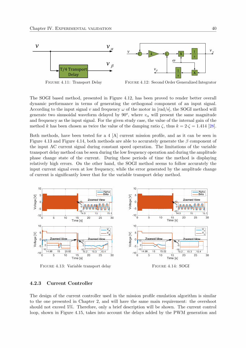
Chapter IV. Experimental validation 40
T/4 TransportDelay
vv
v
Figure 4.11: Transport Delay
v
v
+-
k +- xs
1
xs
1
v
Figure 4.12: Second Order Generalized Integrator
The SOGI based method, presented in Figure 4.12, has been proved to render better overalldynamic performance in terms of generating the orthogonal component of an input signal.According to the input signal v and frequency ω of the motor in [rad/s], the SOGI method willgenerate two sinusoidal waveform delayed by 90o, where vα will present the same magnitudeand frequency as the input signal. For the given study case, the value of the internal gain of themethod k has been chosen as twice the value of the damping ratio ζ, thus k = 2·ζ = 1.414 [28].
Both methods, have been tested for a 4 [A] current mission profile, and as it can be seen inFigure 4.13 and Figure 4.14, both methods are able to accurately generate the β component ofthe input AC current signal during constant speed operation. The limitations of the variabletransport delay method can be seen during the low frequency operation and during the amplitudephase change state of the current. During these periods of time the method is displayingrelatively high errors. On the other hand, the SOGI method seems to follow accurately theinput current signal even at low frequency, while the error generated by the amplitude changeof current is significantly lower that for the variable transport delay method.
Figure 4.13: Variable transport delay Figure 4.14: SOGI
4.2.3 Current Controller
The design of the current controller used in the mission profile emulation algorithm is similarto the one presented in Chapter 2, and will have the same main requirement: the overshootshould not exceed 5%. Therefore, only a brief description will be shown. The current controlloop, shown in Figure 4.15, takes into account the delays added by the PWM generation and

Chapter IV. Experimental validation 41
by the current measurement, which are modelled as first order systems, with a sample time ofTs = 1/fsw = 0.0625[ms]. According to the load used in experimental setup, the plant transferfunction can be derived as follows:
G(s) =1
L · s+R(4.6)
where, L represents the inductance and R is the internal resistance of inductor. Since the valueof the internal resistance was not specified on the nameplate of the inductor, it is assumed equalto 0.001[Ω].
15.0
1
sTs)1(
1
sR
15.0
1
sTs
Control Delay Plant
Sampling Delay
s
KK i
p
PI Controller
qi
qi
*
qi
Figure 4.15: Current control loop
Similarly, to the motor drive current PI design, the Optimal Modulus criterion is applied,resulting in the following values of the proportional and integral gains:
Kp = 12.27
Ki = 101.3
Based on the determined controller parameters, the Bode diagram of the open loop system isplotted in Figure 4.16, and it can be seen the system is stable. Moreover, from the step responseof the closet loop system, presented in Figure 4.17, it can be concluded that the controller meetsthe imposed requirement, due to the fact that the overshoot is equal to 4.75%.
Magn
itu
de
(dB
)
-50
0
50
100
150
10-2
100
102
104
Ph
ase
(d
eg)
-270
-225
-180
-135
-90
Bode DiagramGm = 18.1 dB (at 3.2e+04 rad/s) , Pm = 63.3 deg (at 7.57e+03 rad/s)
Frequency (rad/s)
Figure 4.16: Current Control - Bode Diagram
#10-4
0 1 2 3 4 5 6 70
0.2
0.4
0.6
0.8
1
1.2
Step ResponseOvershoot = 4.75 [%], Tr = 0.1 [ms]
Time (seconds)
Am
plit
ud
e
Figure 4.17: Current Control - Step Response

Chapter IV. Experimental validation 42
4.3 Simulation and Experimental Results
The above mentioned model has been implemented in MATALB/Simulink and linked with thedSpace system, with a sample time of Ts = 1/16000[s]. The experiment was run at 660V DCinput, and the output AC voltage of the inverter can be seen Figure 4.19. It can be observedthat the test and load leg voltages are in phase and that the waveforms are generated in threevoltage steps (Vdc/2, 0 and −Vdc/2) due to the three level configuration of the NPC.
T1
T2
T3
T4
Figure 4.18: Test leg PWM
vAN vBN
Figure 4.19: Inverter output voltage
In Figure 4.20 the simulation results obtained after emulating the motor drive speed and torquemission profiles, on the three level NPC H-bridge can be seen. It can be noticed that emulationis performed in a correct manner, the obtained waveforms, resembling the current and voltageresponse of the PMSM. In order to highlight the correlation between the voltage and current,the plotted voltage waveform has been divided by a factor of 10.
Figure 4.20: Normal operation - Mission profile
The results obtained from running the experiment at Normal Operation mission profile canbe seen in Figure 4.21. From the full view of a single cycle of the mission profile, shown inFigure 4.21a, it can be observed that the current waveform matches the simulation results, withsome minor errors on the deceleration period.

Chapter IV. Experimental validation 43
vAN
IAC
(a) Mission Profile - Full view
IAC
vAN
(b) Zoomed View - Constant speed
IAC
vAN
(c) Zoomed View - Deceleration
IAC
vAN
(d) Zoomed View - Acceleration
Figure 4.21: Normal operation mission profile

Chapter IV. Experimental validation 44
During the constant speed operation the current reaches the reference 10 [A] value and runs inphase with the test leg voltage at a frequency of approximately 73 [Hz]. Although, during theacceleration period the system behaves as expected, with the current hitting its estimated 12[A] value, during the deceleration period the current presents a long response time reaching itsreference value in roughly 0.2 [s]. This is mainly due to the error rendered by the OSG blockwhen the current goes through a large amplitude change (from 10 [A] to -12 [A]). Moreover, asthe frequency of the drive is decreasing the error caused by the variable time delay increases,which will result in high noise in the current waveform, as shown in Figure 4.21c.
In order to solve this problem, the Second Order Generalized Integrator (SOGI) was used togenerate the quadrature of the output current, but the discrete-time domain implementationof this method rendered a similar error during the low frequency operation. Therefore, due totime limitations, this issue was no longer investigated and the variable transport delay basedOSG has been employed for the other cases.
A. Deceleration Slope Adjustment
In the following the decreased deceleration slope mission profile is presented. In Figure 4.22 thesimulation results are presented.
Figure 4.22: Deceleration Slope Adjustment - Mission profile
In Figure 4.23, the results obtained from emulating the Decreased Deceleration Slope profilecan be seen. As expected, during the deceleration period, the amplitude of the current issignificantly reduced, but similarly to the previous case, a long response time can be observed.The behaviour of the current in the acceleration and constant speed time periods is identical tothe Normal Operation mission profile.

Chapter IV. Experimental validation 45
IAC
vAN
(a) Mission Profile - Full view
IAC
vAN
(b) Zoomed View - Deceleration
Figure 4.23: Decreased deceleration slope mission profile
B. Reactive Current Injection
In the following, the system response will be analyzed during the reactive current injection case,as shown in Figure 4.25, while the simualtion results are shown in Figure 4.24.
Figure 4.24: Reactive Current Injection - Mission profile

Chapter IV. Experimental validation 46
IAC
vAN
(a) Mission Profile - Full view
IAC
vAN
(b) Zoomed View - Constant speed
IAC
vAN
(c) Zoomed View - Deceleration
IAC
vAN
(d) Zoomed View - Acceleration
Figure 4.25: Reactive current injection mission profile

Chapter IV. Experimental validation 47
By injecting reactive current (i∗d = −10[A]) into the system, the expected current amplitude willincrease in comparison with the previous two cases. In Figure 4.25b - Figure 4.25d, it can alsobe observed that the current waveform is leading the voltage. On the other hand, if the injectedreactive current is positive (i∗d = 10[A]) the current will be lagging the voltage, as presented inFigure 4.27, while the simualation results for pozitive reactive current injection are shown inFigure 4.26
Figure 4.26: Reactive Current Injection - Mission profile
IACvAN vBN
Figure 4.27: Zoomed View - Constant speed
C. Switching Frequency Adjustment
At this point it should be noted that the Decreased Switching Frequency case was not analyzed,due to the limitations of the dSpace system, which can not change the fixed-step sample sizeduring a real-time simulation.

Chapter 5
Conclusions
In this thesis, three active thermal control methods for the power semiconductor devices ofthe motor drive application have been investigated.The motor drive system together with thethermal loading which occurs in the power semiconductor devices has been modelled and thedynamic behaviour of the system has been analyzed under certain speed and torque missionprofiles. During the acceleration and the deceleration periods of the motor, large thermal cycles,could be observed in the power devices. It has been concluded that the main causes for thislarge temperature swings are the amplitude of the load current of the machine and the lowfundamental frequency. Additionally, the influence of the parameters involved in the power lossmodelling has been investigated and it has been concluded that the switching frequency and theDC link voltage will have a significant impact on the thermal stress to which the power devicesare subject to.
In order to solve the aforementioned problem, three active thermal control have been imple-mented. The Switching Frequency Adjustment method consists of decreasing the switchingfrequency of the converter, and therefore reducing the switching losses of the devices. Themethod has proved effective in decreasing the amplitude of the amplitude of the thermal cycles,but due to the low switching loss characteristics of the power devices used as study case, theimpact of the method is not significant.
Afterwards, the Reactive Current Injection method has been analyzed, managing to eliminatethe large temperature drop from the braking period of the motor, thus leading to a more uniformthermal distribution. Finally, the Deceleration Slope Adjustment method has been investigated,and it has been concluded that it is the most effective algorithm among the other presented, forthe given application.
In order to validate the simulation results, a motor drive mission profile algorithm has beendeveloped. The speed and torque mission profiles have been translated to the reference voltageand current values needed within the experimental setup control algorithm. The AC currentcontroller used in the mission profile emulation has been design, and an orthogonal signal gener-ator has been implemented. By employing the algorithm, the speed and torque mission profilewere successfully emulated on the inductive load of the experimental setup, thus validating theemulation technique simulation results.
5.1 Future work
One of the first steps that should be followed as future work, is to measure the thermal loadingon the open IGBT module. A layer of black paint has been applied to the power module, asshown in Figure 5.1, in order to facilitate an accurate temperature measurement of the junctiontemperatures of the power semiconductor devices.
48

Chapter V. Conclusions 49
(a) Before (b) After
Figure 5.1: IGBT open module
Once the actual thermal measurement validate the obtained thermal results, the active thermalcontrol algorithms can be implemented in the experimental setup, in order to confirm theeffectiveness of the methods.
Additionally, the problem of the orthogonal signal generation should be further investigated,especially for the low fundamental frequency operation.

Bibliography
[1] N. Mohan, T.M. Undeland, and W.P. Robbins. Power Electronics: Converters, Applica-tions and Design. John Wiley and Sons Inc., 2014.
[2] L.M. Moore and H.N. Post. Five Years of Operating Experience at a Large, Utility-scalePhotovoltaic Generating Plant. Prog. Photovolt: Res. Appl., 2008.
[3] Juan Bueno Gayo. Reliability-focused research on optimizing Wind Energy system design,operation and maintenance: Tools, proof of concepts, guidelines & methodologies for a newgeneration. 2011.
[4] S. Yang, A. Bryant, P. Mawby, D. Xiang, L. Ran, and P. Tavner. An Industry-Based Surveyof Reliability in Power Electronic Converters. 2009.
[5] ZVEI: Die Elektroindustrie. Handbook for Robustness Validation of Automotive Electri-cal/Electronic Modules. German Electrical and Electronic Manufacturers Association, June2013.
[6] U.Choi. Studies on IGBT Module to Improve the Reliability of Power Electronic Systems.Aalborg University Press, Feb.2016.
[7] V. Smet, F. Forest, J.-J. Huselstein, F. Richardeau, Z. Khatir, S. Lefebvre, and M. Berkani.Ageing and Failure Modes of IGBT Modules in High-Temperature Power Cycling. IEEETrans. on Industrial Electronics, Vol. 58, No. 10, Oct.2011.
[8] A. Wintrich, U. Nicolai, W. Tursky, and T. Reimann. Semikron: Application ManualPower Semiconductors. SEMIKRON International GmbH, 2015.
[9] M.S. Merzoug and F. Naceri. Comparison of Field-Oriented Control and Direct TorqueControl for Permanent Magnet Synchronous Motor (PMSM). World Academy of Science,Engineering and Technology, 2008.
[10] X.T. Garcia, B. Zigmund, A. Terlizzi, R. Pavlanin, and L. Salvatore. Comparison be-tween FOC and DTC strategies for Permanent Magnet Synchronous Motor. Advances inElectrical and Electronic Engineering, 2006.
[11] G.F. Franklin, J.D. Powell, and A.Naeini. Feedback control of dynamic systems. Boston :Pearson, 2006.
[12] C. Capitan. Torque Control in Field Weakening Mode. Aalborg University Press, 2009.
[13] M. Valentini, T. Ofeigsson, and A. Raducu. Control of a variable speed variable pitch windturbine with full power converter. Aalborg University Press, 2007.
[14] R. Mizera. Modification of Symmetric Optimum Method. ASR 2005 Seminar, Instrumentsand Control, 2005.
[15] A.M. Hava, R.J. Kerkman, and T.A. Lipo. Simple Analytical and Graphical Methodsfor Carrier-Based PWM-VSI Drives. IEEE Trans. on Power Electronics, Vol. 14, no.1, Jan.1999.
50

Bibliography 51
[16] M. Weckert and J. Roth-Stielow. Lifetime as a Control Variable in Power ElectronicSystems. Emobility - Electrical Power Train, Nov.2010.
[17] G. Lo Calzo, A. Lidozzi, L. Solero, F. Crescimbini, and V. Cardi. Thermal Regulation asControl Reference in Electric Drives. Power Electronics and Motion Control Conference(EPE/PEMC), Sept.2012.
[18] A.T. Bryant, P.R. Palmer P.A. Mawby and, E. Santi, and J.L. Hudgins. Exploration ofPower Device Reliability Using Compact Device Models and Fast Electrothermal Simulation.IEEE Trans. on Industry App., Vol. 44, No. 3, June 2008.
[19] K. Ma, A.S. Balunan, S.M. Beczkowski, and F. Blaabjerg. Loss and Thermal Model forPower Semiconductors Including Device Rating Information. The 2014 International PowerElectronics Conference, 2014.
[20] K. Ma and F. Blaabjerg. Multi-timescale Modelling for the Loading Behaviours of PowerElectronics Converter. Proc. of ECCE 2015, pp.5749-5756, 2015.
[21] P.D. Reigosa, H. Wang, Y. Yang, and F. Blaabjerg. Prediction of Bond Wire Fatigue ofIGBTs in a PV Inverter Under a Long-Term Operation. IEEE Trans. on Power Electronics,Vol. 31, No. 10, Oct.2016.
[22] Infineon. Thermal Equivalent Circuit Models: Application Note v1.0. Infineon technologiesAG, Jun.2008.
[23] K. Ma, Y. Yang, and Frede Blaabjerg. Transient Modelling of Loss and Thermal Dynamicsin Power Semiconductor Devices. Proc. of the 2014 IEEE Energy Conversion Congress andExposition (ECCE), 2014.
[24] K. Ma, M. Liserre, and F. Blaabjerg. Reactive Power Influence on the Thermal Cycling ofMulti-MW Wind Power Inverter. IEEE Trans. on Industry Applications, Vol. 49, No. 2,pp.922 - 930, Apr. 2013.
[25] D.A. Murdock, J.E.R. Torres, J.J. Connors, and R.D. Lorenz. Active Thermal Control ofPower Electronic Modules. IEEE TRANSACTIONS ON INDUSTRY APPLICATIONS,VOL. 42, NO. 2, MARCH/APRIL 2006.
[26] M. Andresen, M. Liserre, and G. Buticchi. Review of Active Thermal and Lifetime Con-trol Techniques for Power Electronic Modules. IEEE TRANSACTIONS ON INDUSTRYAPPLICATIONS, VOL. 42, NO. 2, MARCH/APRIL 2006.
[27] U.-M. Choi, I. Trintis, Frede Blaabjerg, S. Jørgensen, and M. L. Svarre. Advanced PowerCycling Test for Power Module with On-line On-state VCE Measurement. IEEE AppliedPower Electronics Conference and Exposition (APEC), Mar.2015.
[28] M. Ciobotaru. Reliable Grid Condition Detection and Control of Single-Phase DistributedPower Generation Systems. Aalborg: Institut for Energiteknik, Aalborg Universitet, 2009.