
Modeling of Plasma Etching Reactors Including Wafer ... · assumed from the edge of the SiO2...
11
J. Electrochem. Soc., Vol. 140, No. 5, May 1993 The Electrochemical Society, Inc. 1471 assumed from the edge of the SiO2 conduction band corre- sponding to the energies of 3.04 and 2.76 eV for the HE region. We cannot surely fred the appropriate energy levels for c-St. These two energy levels also are observed in the oxidation process of hydrogenated amorphous Si (a-St:H). Figure 7 shows the spectra of the emission light during the anodic oxidation of c-St (solid line) and a-Si:H (dashed line), and aluminum (AI) metal. The a-Si:H film with a thickness greater than 300 nm was deposited on a e-St sub- strafe by a plasma chemical vapor deposition (CVD) method. The oxidation process of AI metal was carried out using the same method as in the case of Si oxidation except for the replacement of the electrolyte with a mixture of pure water, citric acid [1.5 weight percent (w/o)], and am- monium citrate (1.5 w/o). The spectrum recorded in the course of A1 oxidation exhibits an emission peak only in the LE region. The spectra of a-Si:H and c-St are almost simi- lar. These experimental results suggest that the interface energy levels for light emission at the SiO2-Si interface may be attributed to the creation of chemical bonding between the SiO2 and Si, and they do not depend on the structure of St. Summary The relation of light emission and anodic oxidation of c-St have been studied. No light emission can be observed until the SiO2 film grows to the thickness 15 nm. After reaching this critical value, the light emission appears and the integrated intensity of the light increases exponentially with SiO2 film thickness having a factor of 10 nm. The spec- trum of the emission light consists of different regions, i.e., LE and HE regions. The LE region has a broad peak corre- sponding to the energy of 1.93 eV and its intensity increases with the thickness of the SiO~ film. The HE region exhibits two peaks of 3.04 and 2.76 eV, regardless of the thickness of the SiO2 film. A-Si:H also shows a similar spectrum. There- fore, the light emission in the LE region is attributed to the emission centers excited by hot electrons accelerated by the high field of about 22 MV/cm in the SiQ layer and in the HE region it is due to the interface levels resulting from the creation of chemical bonds between SiO2 and St. Manuscript submitted Nov. 5, 1992; revised manuscript received Jan. 28, 1993. Shizuoka University assisted in meeting the publication costs of this article. REFERENCES 1. T. H. Ning and H. N. Yu, J. Appl. Phys., 45, 5373 (1974). 2. D. R. Young, ibid., 47, 2098 (1976). 3. J. E Verwey, ibid., 44, 2681 (1973). 4. E. H. Nicollian and C. N. Berglund, ibid., 41, 3052 (1970). 5. R. Williams, Phys. Rev., 146, A569 (1965). 6. T. H. Ning, Solid-State Electron., 21, 273 (1978). 7. L. T. Canham, Appl. Phys. Lett., 57, 1046 (1990). 8. T. Ito, T. Ohta, and A. Hiraki, Jpn. J. Appl. Phys., 31, L1 (1992). 9. N. Koshida and H. Koyama, Appl. Phys. Lett., 60, Jan (1992). 10. Light Emission from Silicon, S. S. Iyer, R. T. Collins, and L. T. Canham, Editors, Material Research Soci- ety, Pittsburgh, PA (1992). 11. Y. Nakanishi, G. Zhou, T. Ando, and G. Shimaoka, Electroluminescence, S. Shionoya and H. Kobayashi, Editors, p. 65. 12. G. Zhou, Y. Nakanishi, and Y. Hatanaka, Semicond. Sci. Tech., 7, B549 (1992). 13. H. Yamamoto et al., Electron. Lett., 19, 6 (1983). 14. C. N. Berglund and R. J. Powell, J. Appl. Phys., 42, 573 (1971). Modeling of Plasma Etching Reactors Including Wafer Heating Effects Eray S. Aydil *'~ and Demetre J. Economou* Department of Chemical Engineering, Plasma Processing Laboratory, University of Houston, Houston, Texas 77204-4792 ABSTRACT A comprehensive mathematical model of chlorine etching of polysilicon in a single-wafer plasma reactor was devel- oped from first principles. Wafer heat transport was included as an integral part of the analysis. The model provided the spatiotemporal variations of etchant concentration, wafer temperature, and etch rate. Under conditions of high etch rate and poor wafer cooling, etching was inherently transient. The polysilicon etch rate increased with time despite the fact that the atomic chlorine concentration decreased with time. This was due to wafer heating and the Arrhenius dependence of etch rate on temperature. Multichannel laser interferometry was developed to monitor the spatiotemporal variations of etch rate in real time. Measured etch rate transients compared favorably with model predictions. Results were sensitive to surface reaction parameters and to wafer back side cooling. Plasma reactor modeling has received considerable at- tention recently in an effort to understand the intricate nature of the glow discharge and the plasma-wafer interac- tion. 1Macroscopic plasma reactor models emphasize either the discharge structure 2 or transport and reaction of neu- tral species including the reaction rate distribution along the wafer surface? The latter models make the assumption of isothermal wafer. However, rapid reaction rates, ion bombardment, and/or poor heat transfer from the wafer can result in significant wafer heating which in turn can affect the etch rate, uniformity, and anisotropy. 4 For exam- ple, Tachi et al. 5 found a 80~ temperature rise during high rate etching of silicon. Wafer heating effects and etch rate transients are becoming increasingly important in plasma * Electrochemical Society Active Member. a Present address: Department of Chemical and Nuclear Engi- neering, University of California, Santa Barbara, CA 93106. etching as high input power and rapid etching are required to maintain high throughput in single-wafer machines. Theoretical studies of wafer heating to date examine the wafer in isolation from the rest of the reactor. 6 This sim- plified approach is not adequate especially when chemical etching makes a contribution. Recently, we developed a comprehensive model of a chlo- rine plasma sustained in a single-wafer reactor. 7 The model was tested using a variety of plasma diagnostics. Electron density and energy, self-sustaining electric field, RF cur- rent flowing through the plasma, ion bombardment energy, and atomic chlorine concentration were found to agree with model predictions over a range of pressure, power, and electrode spacing without adjusting any reaction rate coefficients. This model is expanded in the present work to include wafer heating as an integral part of the analysis. To our knowledge, this is the first model which considers the dy-
Transcript of Modeling of Plasma Etching Reactors Including Wafer ... · assumed from the edge of the SiO2...
J. Electrochem. Soc., Vol. 140, No. 5, May 1993 �9 The Electrochemical Society, Inc. 1471
assumed from the edge of the SiO2 conduction band corre- sponding to the energies of 3.04 and 2.76 eV for the HE region. We cannot surely fred the appropriate energy levels for c-St. These two energy levels also are observed in the oxidation process of hydrogenated amorphous Si (a-St:H). Figure 7 shows the spectra of the emission light during the anodic oxidation of c-St (solid line) and a-Si:H (dashed line), and aluminum (AI) metal. The a-Si:H film with a thickness greater than 300 nm was deposited on a e-St sub- strafe by a plasma chemical vapor deposition (CVD) method. The oxidation process of AI metal was carried out using the same method as in the case of Si oxidation except for the replacement of the electrolyte with a mixture of pure water, citric acid [1.5 weight percent (w/o)], and am- monium citrate (1.5 w/o). The spectrum recorded in the course of A1 oxidation exhibits an emission peak only in the LE region. The spectra of a-Si:H and c-St are almost simi- lar. These experimental results suggest that the interface energy levels for light emission at the SiO2-Si interface may be attributed to the creation of chemical bonding between the SiO2 and Si, and they do not depend on the structure of St.
Summary The relation of light emission and anodic oxidation of
c-St have been studied. No light emission can be observed unti l the SiO2 film grows to the thickness 15 nm. After reaching this critical value, the light emission appears and the integrated intensity of the light increases exponentially with SiO2 film thickness having a factor of 10 nm. The spec- t rum of the emission light consists of different regions, i.e., LE and HE regions. The LE region has a broad peak corre- sponding to the energy of 1.93 eV and its intensity increases with the thickness of the SiO~ film. The HE region exhibits two peaks of 3.04 and 2.76 eV, regardless of the thickness of
the SiO2 film. A-Si:H also shows a similar spectrum. There- fore, the light emission in the LE region is at tr ibuted to the emission centers excited by hot electrons accelerated by the high field of about 22 MV/cm in the SiQ layer and in the HE region it is due to the interface levels resulting from the creation of chemical bonds between SiO2 and St.
Manuscript submitted Nov. 5, 1992; revised manuscript received Jan. 28, 1993.
Shizuoka University assisted in meeting the publication costs of this article.
REFERENCES 1. T. H. Ning and H. N. Yu, J. Appl. Phys., 45, 5373 (1974). 2. D. R. Young, ibid., 47, 2098 (1976). 3. J. E Verwey, ibid., 44, 2681 (1973). 4. E. H. Nicollian and C. N. Berglund, ibid., 41, 3052
(1970). 5. R. Williams, Phys. Rev., 146, A569 (1965). 6. T. H. Ning, Solid-State Electron., 21, 273 (1978). 7. L. T. Canham, Appl. Phys. Lett., 57, 1046 (1990). 8. T. Ito, T. Ohta, and A. Hiraki, Jpn. J. Appl. Phys., 31, L1
(1992). 9. N. Koshida and H. Koyama, Appl. Phys. Lett., 60, Jan
(1992). 10. Light Emission from Silicon, S. S. Iyer, R. T. Collins,
and L. T. Canham, Editors, Material Research Soci- ety, Pittsburgh, PA (1992).
11. Y. Nakanishi, G. Zhou, T. Ando, and G. Shimaoka, Electroluminescence, S. Shionoya and H. Kobayashi, Editors, p. 65.
12. G. Zhou, Y. Nakanishi, and Y. Hatanaka, Semicond. Sci. Tech., 7, B549 (1992).
13. H. Yamamoto et al., Electron. Lett., 19, 6 (1983). 14. C. N. Berglund and R. J. Powell, J. Appl. Phys., 42, 573
(1971).
Modeling of Plasma Etching Reactors Including Wafer Heating Effects
Eray S. Aydil *'~ and Demetre J. Economou* Department of Chemical Engineering, Plasma Processing Laboratory, University of Houston, Houston, Texas 77204-4792
ABSTRACT
A comprehensive mathematical model of chlorine etching of polysilicon in a single-wafer plasma reactor was devel- oped from first principles. Wafer heat transport was included as an integral part of the analysis. The model provided the spatiotemporal variations of etchant concentration, wafer temperature, and etch rate. Under conditions of high etch rate and poor wafer cooling, etching was inherently transient. The polysilicon etch rate increased with time despite the fact that the atomic chlorine concentration decreased with time. This was due to wafer heating and the Arrhenius dependence of etch rate on temperature. Multichannel laser interferometry was developed to monitor the spatiotemporal variations of etch rate in real time. Measured etch rate transients compared favorably with model predictions. Results were sensitive to surface reaction parameters and to wafer back side cooling.
Plasma reactor modeling has received considerable at- tention recently in an effort to understand the intricate nature of the glow discharge and the plasma-wafer interac- tion. 1 Macroscopic plasma reactor models emphasize either the discharge structure 2 or transport and reaction of neu- tral species including the reaction rate distribution along the wafer surface? The latter models make the assumption of isothermal wafer. However, rapid reaction rates, ion bombardment, and/or poor heat transfer from the wafer can result in significant wafer heating which in turn can affect the etch rate, uniformity, and anisotropy. 4 For exam- ple, Tachi et al. 5 found a 80~ temperature rise during high rate etching of silicon. Wafer heating effects and etch rate transients are becoming increasingly important in plasma
* Electrochemical Society Active Member. a Present address: Department of Chemical and Nuclear Engi-
neering, University of California, Santa Barbara, CA 93106.
etching as high input power and rapid etching are required to maintain high throughput in single-wafer machines. Theoretical studies of wafer heating to date examine the wafer in isolation from the rest of the reactor. 6 This sim- plified approach is not adequate especially when chemical etching makes a contribution.
Recently, we developed a comprehensive model of a chlo- rine plasma sustained in a single-wafer reactor. 7 The model was tested using a variety of plasma diagnostics. Electron density and energy, self-sustaining electric field, RF cur- rent flowing through the plasma, ion bombardment energy, and atomic chlorine concentration were found to agree with model predictions over a range of pressure, power, and electrode spacing without adjusting any reaction rate coefficients.
This model is expanded in the present work to include wafer heating as an integral part of the analysis. To our knowledge, this is the first model which considers the dy-
1472 J. Electrochem. Soc., Vol. 140, No. 5, May 1993 �9 The Electrochemical Society, Inc.
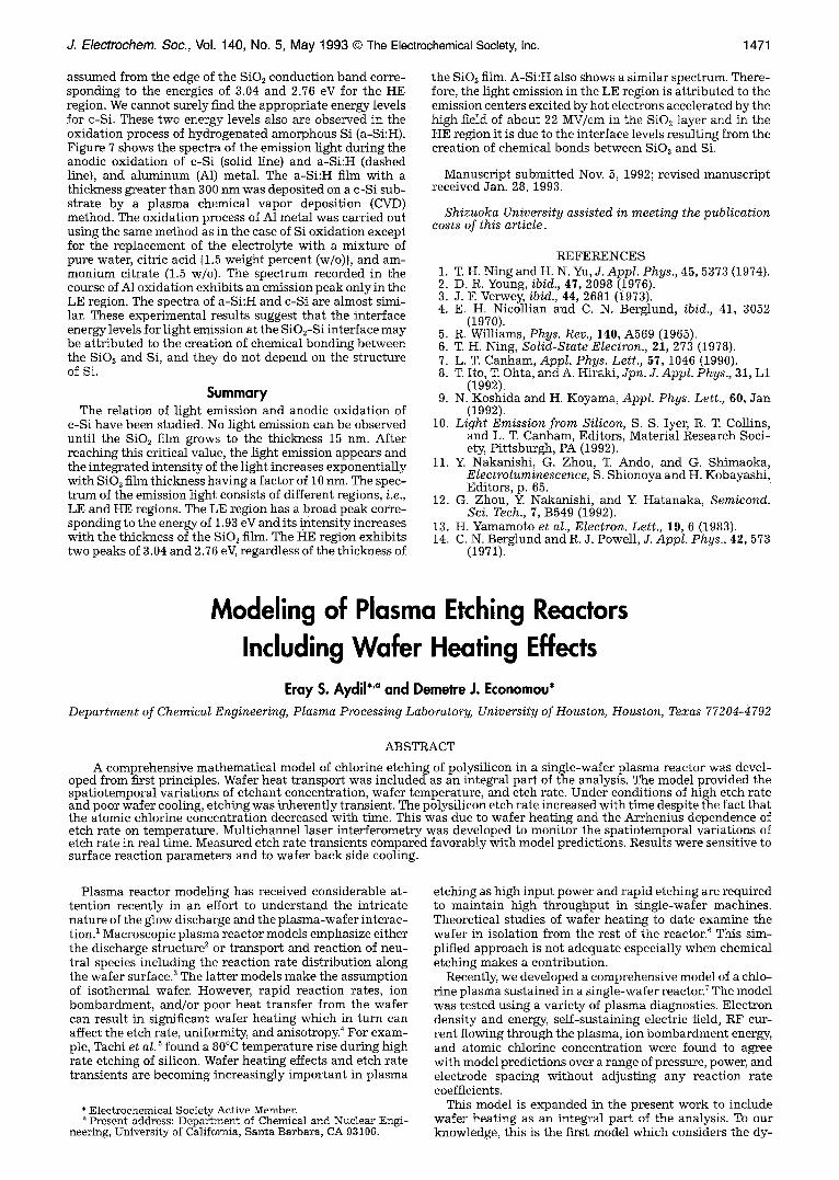
Fig. 1. Overview of modeling approach.
dangm~r Probes I I ~'rnpedance Analysisl T M
tical Emission [ er Fluorescence I~
Laser Interferometry [ AllSpatially Resolved
( RF Power Pressure
BOLTZM~NNARANSPORT / Frequency "~ ~ [ Gas Flow Rate
l Geometry (Electrode, Spacin~ L Pl~ma Radius)
I l [ k j , v d, ]-t e, D o fCE) l
BULK PLASMA MODEL
; ( Sheath Potential V. )~
l AND REACTION MODEL
WAFER HEAT TRANSPORT
IOutputs [ c,(r,z,t), E.R.(r.O. T,(r,t) [ _ _ 1 Modules
namic interaction of wafer heating with radical transport and reaction. The details of wafer heating are presented and experimental data on polysilicon etching using chlo- rine are compared to theoretical predictions. In comparison with the experimental data, the thermal accommodation coefficient on the back side of the wafer was the only ad- justable parameter used. Multichannel laser interferome- try was also developed to monitor the spatiotemporal vari- ations of etch rate in real time.
Model Development Integration of discharge physics and chemistry with rad-
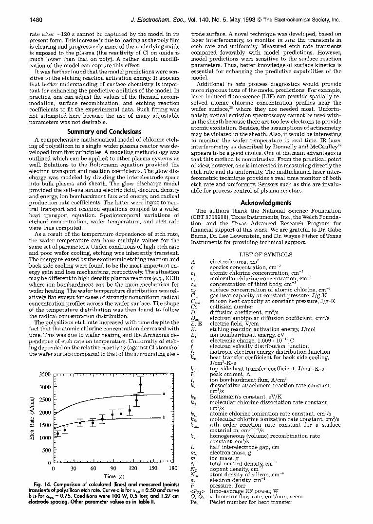
ical transport and reaction in a self-consistent global plasma reactor model is a formidable task from the compu- tational point of view. The work of Kushner and co-work- ers is a notable step towards this goal) Including wafer heating in a global reactor model complicates matters even further. This is due to the disparate time scales involved; plasma electrons respond on a nanosecond time scale whereas the wafer temperature changes on a time scale of minutes. To resolve this problem, a different approach was taken in modeling the glow discharge, whereby the inter- electrode space was divided into two regions: bulk plasma and sheath. This two-region approach was first taken to analyze etching of polymers in oxygen plasmas. 9 However, the bulk plasma model used in the oxygen discharge work was greatly simplified. The two region approach was also followed in a more recent work 7 which included a rather detailed bulk plasma model. In the present work, the model of Ref. 7 was extended further by including wafer heat transport. The advantage of the two-region approach is that it can be readily integrated with radical transport in the gas phase and heat transport in the semiconductor wafer.
A schematic of the modeling approach is depicted in Fig. 1, showing the different models, model inputs, and outputs. The Boltzmann transport equation was used to calculate the electron transport properties and electron- heavy particle reaction rate coefficients. These coefficients were parameterized and used in a bulk plasma model to calculate the self-consistent electric field, electron density, and electron energy. The bulk plasma model also provided the rate coefficients for radical production which were in turn used in a radical transport and reaction model. The latter was coupled with a model for wafer heat transport. The final output was the space and time variations of radi- cal density, wafer temperature, and etch rate. In general the models are coupled with one another. For example, the rad-
ica] transport and reaction model provides the gas compo- sition which in turn affects the electron energy distribution function. The latter affects the electron impact reaction rate coefficients and therefore the plasma gas composition. In addition, the radical concentration is coupled to the wafer temperature. As the wafer temperature increases so does the etch rate resulting in stronger depletion of radicals.
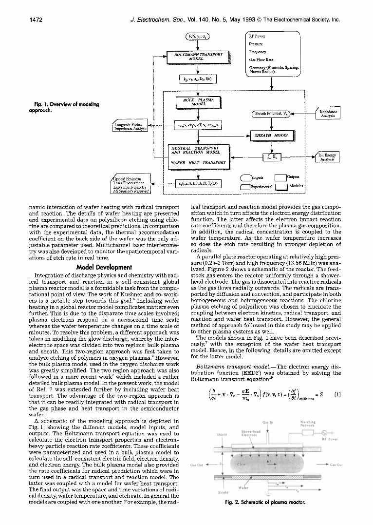
A parallel plate reactor operating at relatively high pres- sure (0.25-2 Tort) and high frequency (13.56 MHz) was ana- lyzed. Figure 2 shows a schematic of the reactor. The feed- stock gas enters the reactor uniformly through a shower- head electrode. The gas is dissociated into reactive radicals as the gas flows radially outwards. The radicals are trans- ported by diffusion and convection, and participate in both homogeneous and heterogeneous reactions. The chlorine plasma etching of polysilicon was chosen to elucidate the coupling between electron kinetics, radical transport, and reaction and wafer heat transport. However, the general method of approach followed in this study may be applied to other plasma systems as well.
The models shown in Fig. 1 have been described previ- ously, 7 with the exception of the wafer heat transport model. Hence, in the following, details are omitted except for the latter model.
Boltzmann transport model.--The electron energy dis- tr ibution function (EEDF) was obtained by solving the Boltzmann transport equation 1~
~f (~+v.V,-~:.vv)f(r,v,t):(~)~,~isioos:s [1]
Fig. 2. Schematic of plasma reactor.
J. Electrochem. Soc., Vol. 140, No. 5, May 1993 �9 The Electrochemical Society, Inc.
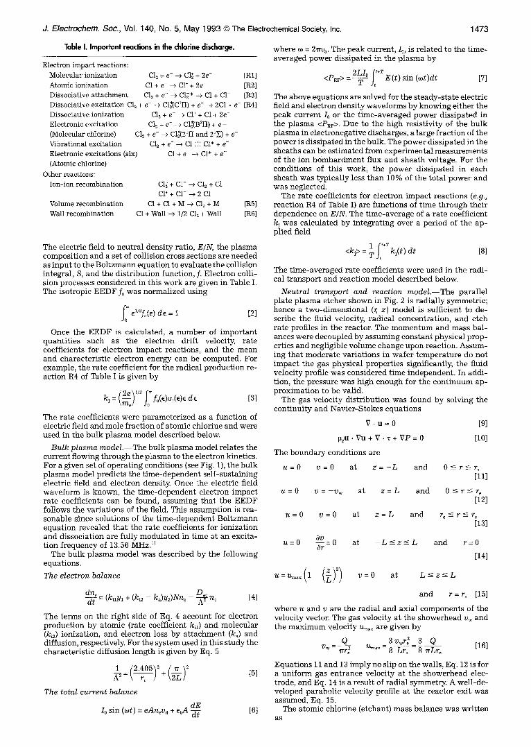
Table I. Important reactions in lhe chlorine discharge.
Electron impact reactions: Molecular ionization C12 + e --> C]~ + 2e- [R1] Atomic ionization C1 + e- --+ C1 + + 2e [R2] Dissociative attachment C12 + e- ---> CI~* --> C1 + C1 [R3] Dissociative excitation C12 + e- -~ Cl~C~l]) + e- -~ 2C1 + e [R4] Dissociative ionization C12 + e --~ C1 + + C1 + 2e- Electronic excitation C12 + e- --+ CI~B3H) + e - (Molecular chlorine) C12 + e- ~ C1~21H and 2~X) + e Vibrational excitation Electronic excitations (six) (Atomic chlorine)
Other reactions: Ion-ion recombination
CI: + e- --* C1 "'" CI* + e C1 + e- ~ CI* + e-
CI~ + Cl- --+ Cl2 + Cl
Cl+ + CI- --~ 2 Cl
Volume recombination C1 + C1 + M --> CI2 + M [R5]
Wall recombination Cl + Wall --+ 1/2 C12 + Wall [R6]
The e lect r ic field to n e u t r a l dens i ty ra t io , E/N, t h e p l a s m a compos i t i on a n d a set of col l is ion cross sec t ions are n e e d e d as i n p u t to the B o l t z m a n n e q u a t i o n to eva lua t e t he col l is ion in tegra l , S, a n d the d i s t r i b u t i o n func t ion , f. E l ec t ron coll i- s ion processes cons ide red in th i s w o r k are g iven in Table I. The i so t rop ic E E D F fo was n o r m a l i z e d u s ing
ff elJ2fo(e) d e = 1 [2]
Once the E E D F is ca lcu la ted , a n u m b e r of i m p o r t a n t q u a n t i t i e s such as the e lec t ron dr i f t velocity, r a t e coeff icients for e l ec t ron i m p a c t reac t ions , a n d the m e a n a n d cha rac t e r i s t i c e l ec t ron ene rgy can be computed . Fo r example , t he r a t e coeff icient for the r ad i ca l p r o d u c t i o n re- ac t ion R4 of Table I is g iven b y
\me/
The r a t e coeff icients were p a r a m e t e r i z e d as a f u n c t i o n of e lec t r ic field a n d mole f r a c t i o n of a tomic ch lo r ine a n d were u sed in the b u l k p l a s m a mode l desc r ibed below.
B u l k p lasma m o d e L - - T h e b u l k p l a s m a m o d e l r e l a t e s the c u r r e n t f lowing t h r o u g h the p l a s m a to the e l ec t ron kinet ics . Fo r a g iven set of o p e r a t i n g cond i t ions (see Fig. 1), t he b u l k p l a s m a mode l p red ic t s the t i m e - d e p e n d e n t s e l f - sus t a in ing e lect r ic field a n d e l ec t ron density. Once the e lect r ic field w a v e f o r m is k n o w n , the t i m e - d e p e n d e n t e l ec t ron i m p a c t r a t e coeff icients can be found, a s s u m i n g t h a t the E E D F fol lows t he v a r i a t i o n s of t he field. This a s s u m p t i o n is r ea - sonab l e s ince so lu t ions of the t i m e - d e p e n d e n t B o l t z m a n n e q u a t i o n revea led t h a t the r a t e coeff icients for i o n i z a t i o n a n d d i s soc ia t ion are fu l ly m o d u l a t e d in t ime a t a n exc i t a - t ion f r e q u e n c y of 13.56 MHz. n
The b u l k p l a s m a mode l was desc r ibed b y the fo l lowing equa t ions .
The electron balance
dne dt = (kilYl + (ki2 - ka)y2)Nne - ~ n~ [4]
The terms on the right side of Eq. 4 account for electron production by atomic (rate coefficient ki~) and molecular (ki2) ionization, and electron loss by attachment (k,) and diffusion, respectively. For the system used in this study the characteristic diffusion length is given by Eq. 5
- - - - -b
The total current balance
dE I0 s in (cot) = eAn~vd + eoA
[5]
[6]
1473
w h e r e r = 2~ru,. The p e a k cu r ren t , I0, is r e l a t e d to the t ime- a v e r a g e d p o w e r d i s s ipa t ed in t he p l a s m a b y
2Llo f t+r E(t ) s in (cot)dr [7] <PRF> = T
The above equa t i ons are so lved for the s t e a d y - s t a t e e lec t r ic field a n d e lec t ron dens i ty w a v e f o r m s b y k n o w i n g e i the r the p e a k c u r r e n t I0 or the t i m e - a v e r a g e d p o w e r d i s s ipa t ed in the p l a s m a <PaF>. Due to the h i g h res i s t iv i ty of the b u l k p l a s m a in e l ec t ronega t ive d ischarges , a la rge f r a c t i o n of the p o w e r is d i s s ipa t ed in the bulk . The p o w e r d i s s ipa t ed in the shea th s c an be e s t i m a t e d f rom e x p e r i m e n t a l m e a s u r e m e n t s of t he ion b o m b a r d m e n t f lux a n d s h e a t h vol tage. For the cond i t ions of th i s work , t he p o w e r d i s s ipa t ed in each s h e a t h was typ ica l ly less t h a n 10% of the to ta l p o w e r a n d was neglec ted .
The r a t e coeff icients for e lec t ron i m p a c t r eac t ions (e.g., r eac t i on R4 of Table I) are func t i ons of t ime t h r o u g h t h e i r d e p e n d e n c e on E/N. The t i m e - a v e r a g e of a r a t e coeff icient k i was ca l cu la t ed b y i n t e g r a t i n g over a p e r i o d of t he ap - p l ied field
1 ;t+r <kj> = ~ Jt kj(t) dt [8]
The t i m e - a v e r a g e d r a t e coefficients were used in the r a d i - cal t r a n s p o r t a n d r eac t i on mode l desc r ibed below.
Neutral transport and reaction m o d e L - - T h e pa ra l l e l p l a t e p l a s m a e tche r s h o w n in Fig. 2 is r ad i a l l y symmet r ic ; h e n c e a t w o - d i m e n s i o n a l (r, z) m o d e l is suff ic ient to de - scr ibe the f luid velocity, r a d i c a l concen t r a t i on , a n d e t ch r a t e profi les in the reactor. The m o m e n t u m a n d mass b a l - ances were decoup]ed b y a s s u m i n g c o n s t a n t phys ica l p r o p - er t ies a n d neg l ig ib le vo lume c h a n g e u p o n reac t ion . A s s u m - ing t h a t m o d e r a t e v a r i a t i o n s in w a f e r t e m p e r a t u r e do no t i m p a c t the gas phys ica l p rope r t i e s signif icantly, t he f luid ve loc i ty profi le was cons ide red t ime i n d e p e n d e n t . In add i - t ion, the p ressu re was h i g h e n o u g h for the c o n t i n u u m ap - p r o x i m a t i o n to be val id .
The gas ve loc i ty d i s t r i b u t i o n was f o u n d b y so lv ing t he c o n t i n u i t y a n d N a v i e r - S t o k e s equa t i ons
V �9 u = 0 [9]
p~u. Vu + V . -~ + VP = 0 [10]
The b o u n d a r y cond i t ions are
u = 0 v = 0 a t z = - L a n d
u = 0 v = - v ~ a t z = L a n d
u = 0 v = 0 at z = L a n d
OV u=O ~ = 0
O<_r<_r~ [11]
O < _ r ~ r e [12]
re<_ r<_ rs [13]
at - L - < z-< L a n d r = 0
[14]
v=O a t - L < - z < - L
a n d r = rs [15]
whe re u a n d v are the r a d i a l a n d ax ia l c o m p o n e n t s of the ve loc i ty vector. The gas ve loc i ty a t the s h o w e r h e a d vw a n d the m a x i m u m veloc i ty Umax are g iven b y
Q 3vwr~ 3 Q [16] vw - ~rr~ Umax -- 8 Lr, - 8 ~rLrs
E q u a t i o n s 11 a n d 13 imp ly no sl ip on the walls , Eq. 12 is for a u n i f o r m gas e n t r a n c e ve loc i ty a t the s h o w e r h e a d elec- t rode, a n d Eq. 14 is a r e su l t of r a d i a l symmetry. A we l l -de - ve loped p a r a b o l i c ve loc i ty profi le a t t he r e ac to r ex i t was assumed, Eq. 15.
The a tomic ch lo r ine (e tchan t ) mass b a l a n c e was w r i t t e n a s
1474 J. Electrochem. Soc., Vol. 140, No. 5, May 1993 �9 The Electrochemical Society, Inc.
0cl DlV2cl + u . Vcl - [(2k~ + ka)ne]C 2 + k2C2CM -- 0 [17] 0t
The atom concentration cannot respond to the rapid varia- tfons of the plasma excitation field. However, wafer tem- perature transients can have a time constant of the order of minutes. Since radical concentration is affected by wafer temperature, Eq. 17 includes a time dependent term to ac- count for these transients.
The term in brackets in Eq. 17 is the t ime-averaged pro- duction rate coefficient of atomic chlorine calculated from Eq. 8. This term couples the Boltzmann transport model, bulk plasma model, and etchant transport and reaction model. It should be noted that the production rate coeffi- cient is a function of atomic chlorine concentration c~ since the EEDF depends on c~. Furthermore c~ is a function of position in the reactor making the radical production rate coefficient spatially dependent. However, for small atomic chlorine mole fractions (y~ < 0.2) the dependence of the radical production rate coefficient on c~ is weak and its effects are secondary. ~ Under this condition, the etchant production rate coefficient can be considered independent of position, and is then only a function of pressure, power, and reactor geometry. At relatively high pressure atomic chlorine is eliminated via the homogeneous recombination reaction R5 of Table I, where M is a third body. This reac- tion is represented by the last term on the left side of Eq. 17. The initial condition for Eq. 17 was taken as the steady- state concentration profile corresponding to a wafer tem- perature equal to the electrode temperature.
Etching and wall recombination reactions enter the model through the boundary conditions
0c~ _ 0 at r = O, r = rs and Or
- L < z < L
[18]
C?Cl -D1 ~ - v~cl = Rw(Cl) at z = L and 0 < r < ro
[19]
_ n Ocl = R~(Cl) at z = L and r~ < r < r~ ~ 1 0 Z
[20]
D 8c~_ R~(c~) at z = - L and 0 < r< r~ 1 @ Z - -
[21]
where Rw is the wall recombination rate (reaction R6 in Table I) which depends on the wall material and surface condition. In this study a power law dependence was used, namely
R~(c~) = kn~c~ [22]
where kr~ is the n th order reaction rate constant for a sur- face material m. On surfaces undergoing etching boundary condition Eq. 21 is replaced by
a e l ~ , �9 D1 ~ = liwtCi) + Rt(/+ , E+, ci) at z = - L
a n d 0 < r < r , , [23]
where the total etch rate R t may contain an ion-assisted component which depends on the ion flux L and mean ion energy E+. These quantities can be found from a sheath model.
Sheath modeL- -Th i s model has been described before. ~2 The dimensionless ion drift velocity is given by
(-10V*) 2/5 (u*) 2 - (2Co),/~(1 + 2Co)~Z~ [24]
where the collision number is Co = 0.5N kDO't, and the di- mensionless variables are defined as follows
V* eV~ u*= u§ ~ m, - t c B T ~ k ~ T ~ [25]
The sheath voltage is obtained from impedance measure- ments. The average ion bombardment energy was calcu- lated from the drift velocity using
1 1 2 E§ = ~ (~ m+u§ ) [26]
Etching k inet ics . - -There are several UHV studies on etching of silicon with molecular chlorine under conditions simulating the plasma environment. 13'14 In these studies the ion bombardment flux and energy and the C12 flux were controlled separately. However, it is difficult to extrapolate these results to the relatively high pressure conditions of plasma etching. In the present study, the effect of ion bom- bardment was minimized by etching heavily P-doped polysilicon which is thought to etch chemically by C1 atoms. The relevant kinetics was recently investigated by Ogryzlo et al. ;1~ the etch rate is given by
E.R. (A/min)= 4.04 x 10-~8N~~c~ ,[~ exp ( - R ~ ) [27]
where ND is the dopant density and Ea is the activation energy. Equation 27 was adopted here to evaluate Rt a s s u m - i n g that the etching reaction produces SiCI~ which is ex- pected to be the major stable product at high pressure. The loss rate of atomic chlorine per unit area (in atom/cm2-s) is given by
( E a ) Rt = 6.733 • 10-2agNsiN~ 39 " ~ exp - ~ c~ [281
where g is the number of chlorine atoms needed to remove a silicon atom (i.e., g = 4 in this case) and Ns~ is the atom density of silicon.
Wafer heat transport m o d e L - - A s seen by Eq. 28, the etch rate depends exponentially on wafer temperature Ts. A modest temperature rise from 300 to 350 K causes the etch rate to increase by a factor of three. Several studies of wafer heat transport have been reported. ~6-18 However, modeling works to date consider the wafer in isolation and do not account for the coupling between the wafer temper- ature and radical transport.
Neglecting temperature variations along the thickness of the wafer, the wafer energy balance can be writ ten as
where
1 1 RtAH ~ + I+E+ QN = ~ k~c~AHr" + - hT(T~ - T~)
- hB(T~ - T~) - 2 (~sBesi(T: - T 4) [30]
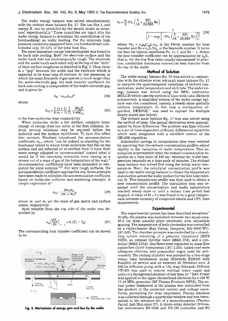
In Eq. 29 the net heat flux to the wafer surface, Q~, is di- vided by the surface to volume ratio (wafer thickness A) to accommodate the surface term into the one-dimensional model. In Eq. 30 the first two terms are heat generation due to surfacerecombinat ion and etching, respectively, which are both exothermic reactions. The third term is the rate of energy transfer to the wafer via energetic ion bombard- ment. The fourth and fifth terms are the rates of energy loss from the wafer top and back side, respectively. The last term is the energy loss via radiation. Energy gain and loss mechanisms and model geometry are depicted in Fig. 3.
Boundary conditions are
0T~ = 0 at r = 0 [31] Or
aT~ -Ks~ ~- = h (T~ - Tg) at r = r~ [32]
Ts = Tc at t = 0 [33]
The no flux boundary condition at the center forces the solution to be symmetric. The initial wafer temperature was taken to be equal to the electrode temperature (Eq. 33). The latter was assumed to be kept constant by cooling wa- ter flow.
J. Electrochem. Soc., Vol. 140, No. 5, May 1993 �9 The Electrochemical Society, Inc. 1475
The wafer energy balance was solved simultaneously with the etchant mass balance Eq. 17. The ion flux L and energy E. can be predicted by the sheath model or meas- ured experimentall S These quantities are input into the wafer energy balance to determine the contribution of ion bombardment on wafer heating. For the relatively high pressure conditions examined here, ion bombardment con- tributed only 10-15% of the total heat flux.
The most important energy loss mechanism was found to be back side cooling. Both the electrode surface and the wafer back side are microscopically rough. The electrode and the wafer touch each other only at the top of the "hills" of their surface roughness as depicted in Fig. 3. Thus, there is a "gap" between the wafer and the electrode which is expected to be some tens of microns. At low pressures, at which the mean free path of gas species is much larger than the wafer-electrode gap, the heat transfer coefficient for back side cooling is independent of the wafer-electrode gap and is given by
where
hn = a,r [34]
1 (7+1) 1 /~kBTr Acl~- 8 (7 - 1) T: ~'~M~cl~ [35]
is the free-molecular heat conductivity. When molecules strike a hot surface, complete inter-
change of energy does not occur at the first collision. In- deed, several collisions may be required before the molecule and the surface equilibrate. To take this effect into account, Knudsen introduced the accommodation coefficient, c~,~, which "can be defined as standing for the fractional extent to which those molecules that fall on the surface and are reflected or re-emitted from it have their mean energy adjusted or 'accommodated' toward what it would be if the returning molecules were issuing as a stream out of a mass of gas at the temperature of the wall." Accommodation coefficients have been measured or esti- mated for some systems, x9'2~ For very rough surfaces, the accommodation coefficient approaches one. Some attempts have been made to calculate the accommodation coefficient based on molecular collision and scattering concepts. A simple expression is ~9
2mlm2 a~cr - (m~ + ~ [36]
where m~ and m2 are the mass of gas specie and surface atoms, respectively.
Heat transfer from the top side of the wafer was de- scribed by
--KS \ d z L= L = hw(T~ - Tg) [37]
The corresponding heat transfer coefficient can be shown to be
Fig. 3. Mechanisms of energy gain and loss by the wafer.
Peh( + 821 Re) 1 3 821
where Peh = VwpsCegL/Kg, is the P6elet number for heat transfer and Re = VwL/2 % is the Reynolds number. It turns out that for typical conditions Peh << 1, and Re - 1. Hence the heat transfer coefficient can be approximated by Kg/L, that is, for the low flow rates usually encountered in prac- tice, conduction dominates convection heat transfer from the top of the wafer.
Method of Solution The wafer energy balance Eq. 29 was solved in conjunc-
tion with the chlorine atom (etchant) mass balance Eq. 17 to compute the spatiotemporal variations of etchant con- centration, wafer temperature and etch rate. The wafer en- ergy balance was solved using the IMSL subroutine MOLCH which uses the method of lines with cubic Hermite polynomials. A simplified version of the wafer energy bal- ance was also considered, namely, a steady-state spatially uniform temperature. In this case a continuation al- gorithm, DERPAR, 21 was used to capture the multiple steady-states (see below).
The etchant mass balance Eq. 17 was also solved using the method of lines. The spatial derivatives were approxi- mated by finite differences. The problem was then reduced to a set of t ime-dependent ordinary differential equations which were integrated with a modified version of the GEARB algorithm.
Substantial savings in computation time were realized by assuming that the etchant concentration profiles adjust rapidly in the variations of wafer temperature. This as- sumption is permissible since the etchant concentration re- sponds on a time scale of 100 ms, whereas the wafer tem- perature responds on a time scale of minutes. The etchant mass balance was solved first using the initial wafer tem- perature. Next, the calculated concentration profile w a s used in the wafer energy balance to obtain the temperature distribution across the wafer surface for the first time inter- va], St. This temperature profile was then used to obtain a new concentration profile. The calculation loop was re- peated until the concentration and wafer temperature reached steady state or until a certain time period had elapsed. A value of ~t = 5 s was found to be a good compro- mise between accuracy of computed results and CPU time requirements.
Experimental The experimental system has been described elsewhere. 7
Briefly, the plasma was sustained between two equal-area, 20.3 cm diam parallel plate electrodes with adjustable spacing. The temperature of both electrodes was controlled by a chiller/heater (Bay Voltex, Tempryte, HS-3500-WC- DC-SX). The chamber pressure was controlled by a closed- loop system consisting of a pressure transducer (MKS 222B), an exhaust throttle valve (MKS 253), and a con- troller (MKS 252A). Gas flows were regulated by mass flow controllers (Unit Instruments UFC-II00). Gases used were ultrapure chlorine, and prepurified argon used for acti- nometry. The etching chamber was pumped by a two-stage rotary vane mechanical pump (Edwards E2M40) with Fomblin oil service and an external oil filtration unit. A 600 i/s diffusion pump with a LN2 trap (Edwards Diffstak CRI60) was used to remove residual water vapor and achieve a background pressure of less than i0 6 Torr. Power was applied to the upper showerhead electrode by a 500 W, 13.56 MHz generator (RF Plasma Products RF5S). The ac- tual power dissipated in the plasma was calculated from the product of the corrected current and voltage wave- forms, accounting for stray impedance. Plasma emission was collected through a quartz side window and was trans- mitted to the entrance slit of a monochromator (Thermo Jarrell Ash Monospec 27). A diode-array detector (Prince- ton Instruments RY-1024 and ST-120 controller and PC
1476 J. Electrochem. Soc., Vol. 140, No. 5, May 1993 @ The Electrochemical Society, Inc.
P.O ~
BEAM SPLITTERS
He-Ne LASER DATA ACQUISITION
TIME
Fig. 4. Schematic of multichannel laser interferometer system.
da t a acquis i t ion) was used to de tec t a n d record spect ra . A smal l a m o u n t (5% by volume) of a r g o n was a d d e d to serve as the a c t i n o m e t e r gas.
The polys i l icon e tch r a t e was m e a s u r e d in situ us ing spa- t ia l ly reso lved l a se r in te r fe romet ry . This t e c h n i q u e is a n ex t ens ion of c o n v e n t i o n a l l ase r in te r fe romet ry . The b e a m f rom a H e - N e l a se r (632.8 nm) was spl i t in to mu l t i p l e b e a m s (four in th i s s tudy) u s ing b e a m spl i t ters . E a c h b e a m was d i r ec t ed a t d i f fe rent r a d i a l pos i t i ons on t he w a f e r (Fig. 4). The ref lected i n t e n s i t y f rom each pos i t i on was m o n i t o r e d u s ing s i l icon pho tode tec to r s . The e t ch ra t e as a f u n c t i o n of pos i t i on was ca l cu la t ed f rom t he i n t ens i t y va r i - a t ions . E t c h r a t e t r a n s i e n t s were also cap tu red . M u l t i c h a n - nel l ase r i n t e r f e r o m e t r y p rov ided a rea l t ime m o n i t o r of the s p a t i o t e m p o r a l v a r i a t i o n s of e t ch rate . This t e c h n i q u e is a t t r a c t i v e for rea l t ime process m o n i t o r i n g a n d c o n t r o l
The heav i ly P - d o p e d polys i l icon wafe r s used in th i s w o r k were p r e p a r e d by Texas I n s t r u m e n t s Inc. The 100 m m d i a m wafe r s h a d a 1000 A oxide layer u n d e r a 4600 A polys i l icon film. The po ly was POCI~ doped a t 950~ for 20 m i n a n d deg lazed in 10 % H F so lu t ion for 1 min. The shee t r e s i s t ance was 16 _+ 3 fl/[:] c o r r e s p o n d i n g to a d o p a n t dens i ty of 1.3 • 102~ cm 3
E t c h i n g of po lys i l icon in a ch lo r ine p l a s m a p re sen t s sev- era l p rob lems . P rev ious r e sea rche r s who h a v e i n v e s t i g a t e d th i s sys tem n o t e d incons i s t enc ies a n d spo rad ic e tching . These were a t t r i b u t e d to the n a t i v e ox ide layer on s i l icon a n d the r e s idua l w a t e r v a p o r in the reactor. The polys i l icon sur face is covered w i t h a n a t i v e ox ide a few tens of a n g s t r o m s th i ck w h i c h does no t e tch w i t h ch lo r ine b u t can be s p u t t e r e d by ions w i t h ene rgy exceed ing - 5 0 eV. 22 In the r eac to r used in t he p r e s e n t work the ion b o m b a r d m e n t en- ergy was no t suff ic ient to r emove the n a t i v e oxide. Hence, t he oxide was r e m o v e d us ing a shor t CF4 p r e - e t c h s tep s im- i l a r to t h a t used by Mogab a n d Levins te in . 23 I n i t i a t i o n of e t ch ing was m o n i t o r e d u s ing l a se r in te r fe romet ry . W h e n CF4 p r e - e t c h was no t used, po lys i l icon d id no t e tch even a f t e r 45 m i n of p l a s m a exposure . In con t ras t , t h e polys i l i - con film was f o u n d to c lea r w i t h i n a few m i n u t e s if e t ch ing was i n i t i a t e d by r emov ing the oxide.
A n o t h e r p r o b l e m w i t h e t ch ing of po lys i l icon is f o r m a t i o n of " b l a c k s i l icon" (somet imes k n o w n as "grass" ) u n d e r cer- t a i n o p e r a t i n g condi t ions . The f o r m a t i o n of grass is a t - t r i b u t e d to " m i c r o m a s k i n g " by ox ide w h i c h yields a r o u g h surface. R o u g h e n i n g of po lys i l icon d u r i n g e t ch ing ha s b e e n r ecen t ly inves t iga ted . 24 I t was conc luded t h a t w a t e r v a p o r was r e spons ib l e for th i s p h e n o m e n a . Cons i s t en t w i t h these s tudies , we f o u n d t h a t a low base p re s su re (<10 -5 Torr) in the e t ch ing c h a m b e r was necessa ry to e tch polys i l icon w i t h o u t f o rming b l a c k sil icon. The e t ch ing c h a m b e r was t hus e v a c u a t e d w i t h a d i f fus ion p u m p for a t l eas t 12 h p r io r to a n etching experiment.
Results and Discussion P a r a m e t e r va lues used for the resu l t s r epo r t ed be low are
s u m m a r i z e d in Table II. These va lues are used for ca lcu la - t ions unless n o t e d o therwise . The p r o b l e m of wa fe r h e a t i n g is d i scussed first fo l lowed by polys i l ieon e t ch ing and com- p a r i s o n w i t h e x p e r i m e n t a l da ta .
Wafer heating.-- In orde r to ga in some u n d e r s t a n d i n g of wa fe r hea t ing , the w a f e r energy b a l a n c e Eq. 29 was f irst so lved i n d e p e n d e n t l y f rom the e t c h a n t mass ba lance . In th i s ease, the sur face ch lo r ine c o n c e n t r a t i o n becomes a free pa ramete r . The s t e a d y - s t a t e spa t i a l ly u n i f o r m w a f e r t em- p e r a t u r e was examined . The w a f e r t e m p e r a t u r e as a r u n e -
Table II. Physical properties and parameter values.
Symbol Name Value
Cusi
ae D, E~ k~q,2 ksi,1 k~l, kiz, kd k~ k~ ND
Qc re r, rw
Vw
ESi h aH~ ano Ksi Kg Aci7 jx~
Psi Pg
heat capacity of silicon gas heat capacity ambipolar diffusivity diffusion coefficient of C1 in C12 etching reaction activation energy 2nd order surface recombination coeff, on SS 1st order surface recombination eoeff, on Si electron-impact reaction coefficients attachment rate coefficient volume recombination coefficient dopant density atomic density of silicon gas flow rate electrode radius shield radius wafer radius gas temperature electrode temperature gas velocity at the showerhcad thermal accommodation coefficient emissivity of silicon wafer thickness heat of C1-C1 recombination heat of etching reaction thermal conductivity of silicon gas thermal conductivity free molecular heat conductivity gas viscosity applied excitation frequency mass density of silicon gas mass density
0.17 cal/g-K 0.116 cal/g-K 3.33 • 10r 250 cm2/s 4700 cal/mol 3.1 • 10 -12 cm~/s 0 cm/s rate calculated through EEDF rate calculated through EEDF 9 X 10 32 emS/s 1.3 X 1020 cm -3 5 X 1022 cm 3 25 sccm 10.15 cm 15.23 cm 5 cm 300 K 293 K 1.073 cm/s 0.41 0.15 0.05 cm 57,300 cal/gmol 342,400 cal/gmol 0.358 cal/cm-s-K 1.78 • 10 5 cal/cm-s-K 0.0024 cal/cm2-s-K-Torr 140 ~P 13.56 MHz 2.33 g/em ~ 1.14 • 10 6 g]cm:~
Note: Physical and transport properties are at 0.3 Torr and 300 K.
J. Electrochem. Soc., Vol. 140, No. 5, May 1993 �9 The Electrochemical Society, Inc. 1477
2000 ' ' ' ~ ' ' ' i ' ' ' i ' ' ' J ' , ,
~- 1600
Melting Pomt of Slhcon
1200
soo
400 A
0 100 2 10 TM 4 10 TM 6 10 TM 8 10 TM 1 1015
Surface CI Concentration (cm 4 )
Fig. 5. Calculated steady-state wafer temperature as a function of surface chlorine atom concentration. Parameter values as in Table II.
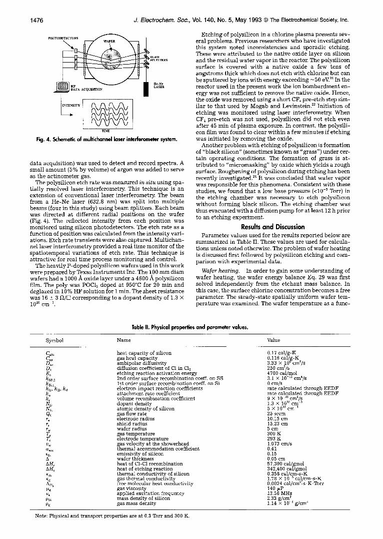
tion of surface chlorine concentration shown in Fig. 5 ex- hibits multiple steady states ( i . e . , more than one possible solutions at the same conditions). This type of behavior is well known (Ref. 25, see also references therein) and arises from the Arrhenius temperature dependence of the etchirig rate (Eq. 28). It is noted that the diagram shown in Fig. 5 was obtained for realistic parameter values. Based on the behavior of similar systems, 2~ _ the upper and lower branches in Fig. 5 are expected to be stable while the mid- dle branch is expected to be unstable. Any value of the surface concentration beyond the limit point A will drive the system towards the upper branch of very high tempera- ture. Of course, the upper branch is not reachable in practice since the melting point of silicon is only 1688 K. In practice, any reasonable thickness of polysilicon film would clear rapidly as the temperature (and hence etch rate) rises, thereby preventing large excursions in tem- perature.
The most important consequence of this multiplicity, however, is that a steady-state wafer temperature may never be reached during etching. For example, when the conditions are such that the upper branch is the only solu- tion (say for a surface chlorine concentration of 8 • 10 ~4 cm -3) etching of any practical thickness of polysilicon film will be inherently transient. A steady-state tempera- ture (and etch rate) cannot be reached before the film clears.
One should note at this point that coupling the etehant mass balance (Eq. 17) to the wafer energy balance has a stabilizing effect in the sense that as the wafer temperature and etch rate increase, the wafer becomes a stronger sink for C1 and the reaction eventually becomes diffusion lim- ited. In other words, the surface C1 concentration would decrease as the etch rate rises (see also Fig. 9 below).
673
"--" 573
473
373
' ~ ' V I . . . . I ' ' . ' I . . . .
273 . . . . . - ~ - r - r ' 7 " . - ] I . . . . i . . . .
0.0 100 5.0 1014 1.0 1015 1.5 1015 2.0 1015 Surface Chlorine Concentration (cm -3)
Fig. 6. Calculated steady-state wafer temperature as a function of surface chlorine atom concentration, a, As in Fig. 5; b, ~~ = 0.41, T~ = 293, ksi,1 -- 1000 cm/s; c, OLac c = 1, Tc = 293, ksi,1 = 0 cm/s; and d, ~o~, = 0.41, T~ = 273, ksu = 0 cm/s.
8000 . . . . I . . . . I . . . . I . . . . ~ . . . . I , , ,,, / /
7000 lxlO15 / I
/ i , I / 9xlO 14,
6000
5000 / "" J t ! !
/ / o . ' ' 8 x 1 0 1 4 . . . 4000
3000 / . - "
2000 f ' " " . . . . . . 6x10¹⁴ I . - ~
1000 Csl=5xlol4cm -3
0 , , , , I , , , , I , i l l [ , , , , I . . . . [ l ~ , ~ : 0 50 100 150 200 250 300
Time (s)
Fig. 7. Calculated etch ra~ tmnsien~ for ~ e conditions of Fig. 5.
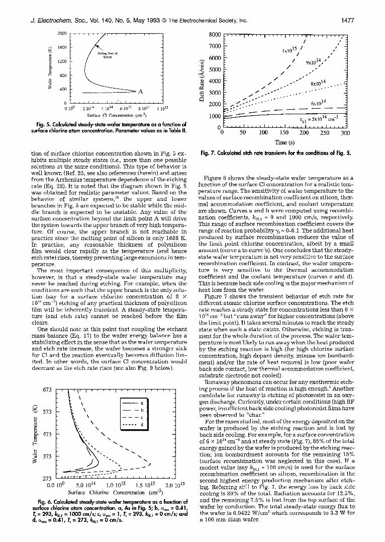
Figure 6 shows the steady-state wafer temperature as a function of the surface C1 concentration for a realistic tem- perature range. The sensitivity of wafer temperature to the values of surface recombination coefficient on silicon, ther- mal accommodation coefficient, and coolant temperature are shown. Curves a and b were computed using recombi- nation coefficients, ksi.1 = 0 and 1000 cm/s, respectively. This range of surface recombination coefficient covers the range of reaction probability % = 0-0.1. The additional heat produced by surface recombination reduces the value of the limit point chlorine concentration, albeit by a small amount (curve a to curve b). One concludes that the steady- state wafer temperature is not very sensitive to the surface recombination coefficient. In contrast, the wafer tempera- ture is very sensitive to the thermal accommodation coefficient and the coolant temperature (curves c and d). This is because back side cooling is the major mechanism of heat loss from the wafer.
Figure 7 shows the transient behavior of etch rate for different atomic chlorine surface concentrations. The etch rate reaches a steady state for concentrations less than 6 • 1014 cm -3 but "runs away" for higher concentrations (above the limit point). It takes several minutes to reach the steady state when such a state exists. Otherwise, etching is tran- sient for the whole duration of the process. The wafer tem- perature is most likely to run away when the heat produced by the etching reaction is high (for high chlorine surface concentration, high dopant density, intense ion bombard- ment) and/or the rate of heat removal is low (poor wafer back side contact, low thermal accommodation coefficient, substrate electrode not cooled).
Runaway phenomena can occur for any exothermic etch- ing process if the heat of reaction is high enough. 4 Another candidate for runaway is etching of photoresist in an oxy- gen discharge. Curiously, under certain conditions (high RF power, insufficient back side cooling) photoresist films have been observed to "char."
For the cases studied, most of the energy deposited on the wafer is produced by the etching reaction and is lost by back side cooling. For example, for a surface concentration of 6 • 1014 cm -3 and at steady state (Fig. 7), 85% of the total energy gained by the wafer is produced by the etching reac- tion; ion bombardment accounts for the remaining 15% (surface recombination was neglected in this case). If a modest value (say ks1.1 = i00 cm/s) is used for the surface recombination coefficient on silicon, recombination is the second highest energy production mechanism after etch- ing. Referring still to Fig. 7, the energy loss by back side cooling is 80% of the total. Radiation accounts for 12.5%, and the remaining 7.5% is lost from the top surface of the wafer by conduction. The total steady-state energy flux to the wafer is 0.0422 W/cm 2 which corresponds to 3.3 W for a i00 mm diam wafer.
1478 J. Electrochem. Soc., Vol. 140, No. 5, May 1993 �9 The Electrochemical Society, Inc.
The wafer heating results discussed so far were for a spatially- uniform surface C1 concentration. The time- and space-dependent wafer energy balance was also solved by using different atomic chlorine surface concentration profiles as input. Three profiles were used
(i) Constant cl~(r) = C1~o [39]
(it) Parabolic decreasing towards the wafer edge
c~(r) = c~o ( 1 - ( ~ ) ~) [40]
(iii) Parabolic increasing towards the wafer edge
(r; cl~(r) = c1~o ~ [41]
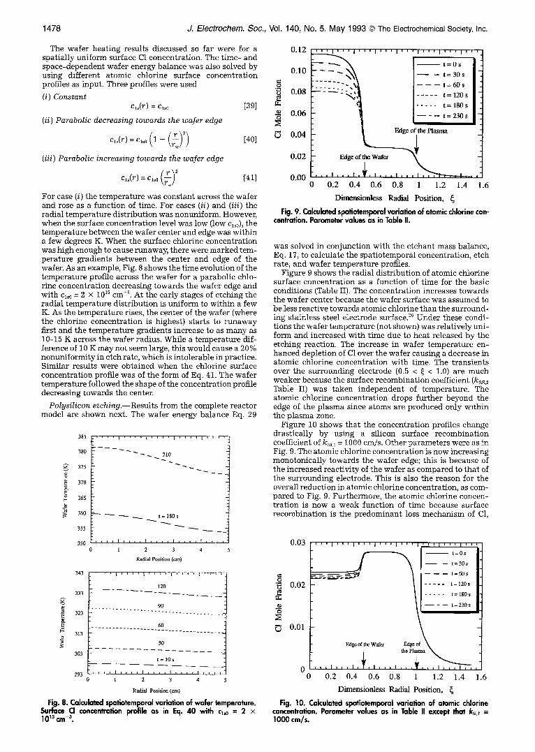
For case (i) the temperature was constant across the wafer and rose as a function of time. For cases (it) and (iii) the radial temperature distribution was nonuniform. However, when the surface concentration level was low (low c~0), the temperature between the wafer center and edge was within a few degrees K. When the surface chlorine concentration was high enough to cause runaway, there were marked tem- perature gradients between the center and edge of the wafer. As an example, Fig. 8 shows the time evolution of the temperature profile across the wafer for a parabolic chlo- rine concentration decreasing towards the wafer edge and with c~0 = 2 • 10 ~ cm -3. At the early stages of etching the radial temperature distribution is uniform to within a few K. As the temperature rises, the center of the wafer (where the chlorine concentration is highest) starts to runaway first and the temperature gradients increase to as many as 10-15 K across the wafer radius. While a temperature dif- ference of 10 K may not seem large, this would cause a 20% nonuniformity in etch rate, which is intolerable in practice. Similar results were obtained when the chlorine surface concentration profile was of the form of Eq. 41. The wafer temperature followed the shape of the concentration profile decreasing towards the center.
Polysilicon etching.--Results from the complete reactor model are shown next. The wafer energy balance Eq. 29
eo
g
8. E
385
380
375
370
365
360
355
350
' ' ~ ' l ' ' ' ' l ' ' ' ' l ' ' ' ' l ' ' ' '
210
-- ~ ~ -_ ._ t = 1 8 0 s
, , , , I , , , , I , , , , I , , , , f , , , ,
l 2 3 4
Radial Position (cm)
343
333
323
313
303
293
120
90 . . . . . . . . . . . . . . . . . . . . . . . . . . . . . . . . . . . . . ~
60
30
t = 10s
1 2 3 4
Radial Position (cm)
Fig. 8. Calculated spafiotemporal variation of wafer temperature. Surface CI concentration profile as in Eq. 40 with q,0 = 2 • I0 is cm -a.
0
o
U
0.12
0.10
0.08
0 . 0 6
0 . 0 4
0.02
0.00
, , , i , , , i , t , l , , , i , , I ' ' ' 1 ' ' ' 1 '
t = 0 S
- - - - t = 3 0 s
- - - - - - t = 6 0 s
. . . . . t= 120s
. . . . . t= 180 s
t = 230 s
Edge o f the P lasma
Zoiw7 , , I , , ~ I I
0 0.2 0.4 0.6 0.8 1 1.2 1.4 1.6
D i m e n s i o n l e s s R a d i a l P o s i t i o n ,
Fig. 9. Calculated spafiotemporal variation of atomic chlorine con- centration. Parameter values as in Table II.
was solved in conjunction with the etchant mass balance, Eq. 17, to calculate the spatiotemporal concentration, etch rate, and wafer temperature profiles.
Figure 9 shows the radial distribution of atomic chlorine surface concentration as a function of time for the basic conditions (Table II). The concentration increases towards the wafer center because the wafer surface was assumed to be less reactive towards atomic chlorine than the surround- ing stainless steel electrode surface. ~6 Under these condi- tions the wafer temperature (not shown) was relatively uni- form and increased with time due to heat released by the etching reaction. The increase in wafer temperature en- hanced depletion of C1 over the wafer causing a decrease in atomic chlorine concentration with time. The transients over the surrounding electrode (0.5 < ~ < 1.0) are much weaker because the surface recombination coefficient (kss,2 Table II) was taken independent of temperature. The atomic chlorine concentration drops further beyond the edge of the plasma since atoms are produced only within the plasma zone.
Figure 10 shows that the concentration profiles change drastically by using a silicon surface recombination coefficient of ks~,i = t000 em/s. Other parameters were as in Fig. 9. The atomic chlorine concentration is now increasing monotonica]]y towards the wafer edge; this is because of the increased reactivity of the wafer as compared to that of the surrounding electrode. This is also the reason for the overall reduction in atomic chlorine concentration, as com- pared to Fig. 9. Furthermore, the atomic chlorine concen- tration is now a weak function of time because surface recombination is the predominant loss mechanism of C1,
0.03
0 '~ 0.02
U 0.01
f ' ' ' I ' ' ' I ' ' ' I ' ' ' I ' ' ~
J ' ' ' 1 ' ' ' 1 ' '
- - t = 0 S
- - - - t = 3 0 S
- - - - - - t = 6 0 S
. . . . . t = 120S
. . . . . t = 1 8 0 S
- - - - t = 2 3 0 S
k Edge of the Wafer Edge of
the Plasma
0 0 0.2 0.4 0.6 0.8 1 1.2 1.4 1.6
Dimensionless Radial Position,
Fig. 10. Calculated spatiotemporal variation of atomic chlorine concentration. Parameter values as in Table II except that ksu = 1000 cm/s.
d. Electrochem. Soc., V o l . 1 4 0 , N o . 5 , M a y 1 9 9 3 �9 T h e E l e c t r o c h e m i c a l
3 4 0 . . . . ~ . . . . ~ . . . . ~ . . . . ~ . . . . t = 230 s t = 180 s
.---. : . - -7 - .= . ~ . . . . . . -..~----. . . . . . . . . . . . . . . . . . . . . . 330 �9 t= 12os
320
310
300
t = 6 0 s
, = 3 0 s . . . . . . . . - - . - 2
t = 0 S
290 , , , , ] , , , , i . . . . I . . . . I . . . . 0 0.1 0.2 0.3 0.4 0.5
Dimensionless Radial Position,
Fig. 11. Calculated spatiotemporal profiles of wafer temperature for the conditions of Fig. 10.
S o c i e t y , Inc. 1 4 7 9
and the corresponding coefficient was assumed independ- ent of tempera ture .
A l though the t ransients in a tomic chlor ine concent ra t ion are weak, the wafe r t empera tu re and e tch ra te va ry consid- e rab ly wi th t ime (Fig. 11 and 12). What is s t r ik ing is that the e tch ra te increases by a fac tor of three in less than 4 min, despi te the fact tha t the e tchant concent ra t ion de- creases dur ing the same period. This is a direct conse- quence of wafe r heat ing. The t empera tu re profiles are re la- t ively flat, and the e tch ra te profiles fo l low the shape of the a tomic chlor ine concentrat ion.
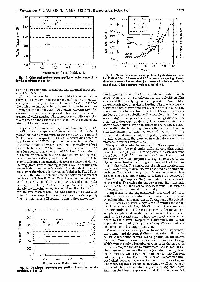
Experimental data and comparison with theory.--Fig- ure 13 shows the space and t ime resolved e tch ra te of polysi l icon for 50 W (nominal power), 0.3 Torr, 25 sccm, and 2.54 cm electrode spacing. The actual power diss ipated in the p lasma was 39 W. The spa t io tempora l var ia t ions of e tch ra te were moni to red in real t ime using spat ia l ly resolved laser interferometry. 27 The a tomic chlorine concent ra t ion as a func t ion of t ime (the rat io of 808.7 nm C1 emission to 811.5 nm Ar emission) is also shown in Fig. 13. The e tch ra te increases dras t ica l ly wi th t ime despite the fact that the a tomic chlorine concent ra t ion decreases somewhat dur ing e tching (from star t of e tching to poin t A). The wafe r edge etches fas ter t han the wafe r center. The edge starts c lear ing 220 s af ter the p lasma is tu rned on (point A in Fig. 13). At this t ime the a tomic chlorine concent ra t ion in the reac tor starts rising. Points B, C, and D indica te the t imes at which the film clears to rad ia l posi t ions of 28, 12, and 0 mm (wafer center), respectively. As the film edge starts c lear ing and the a tomic chlorine concent ra t ion rises, the etch rate in- creases even more rapid ly (see etch ra te at r = 28 mm af ter po in t A, for example). This increase in e tch ra te is par t ly due to an increase in C1 concent ra t ion in the reac tor due to
1200
1000
800
600
a= 400
' ' ' ' I ' ' ' ' I ' ' ~ ' I ' ' ' ' I ' ~ ' ' ~
4 ' t = 230 s t = 180 s _ ~ , ~
t = 120s . . . . . . . . . . . . .
. . . . . . . t----60s . . . . . . . . . . . . /
t = 3 0 s
200
0
t = 0 S ~ .
, , , , l , l , l I i i i i I l i l , l , l , ,
0.1 0.2 0.3 0.4 0.5
D~ensio~ess Radi~ Position,
Fi~. 12. Calculated spatiotemporal profiles of etch rate for the conditions of Fig. 10.
I 4000 ' ' ' I ~ o r=0mm ' ' I . . . . I . . . . 6
i
I . _ / - 3 5 0 0 -qe------] - - -/X - - r = 28 m m I 5
- - - . - ,~,Smm I t ~ i :' 2500
o 2 o o o ,,' I ~= 1500 ~ ,' / "-~
1000 Start of ~ ' ~ . e / A ~" /
.=. E t c h i n g ~ 1
500
O0 . . . . t . . . . w . . . . i . . . . I . . . . i . . . . 0 50 100 150 200 250 300
Time (s)
Fig. 13. Measured spatiotemporal profiles of polysilicon etch rate for 50 W, 0.3 Torr, 25 sccm, and 2.54 cm electrode spacing. Atomic chlorine concentration transient (as measured actinometrically) is also shown. Other parameter values as in Table II.
the fo l lowing reason: the C1 reac t iv i ty on oxide is m u c h lower than that on polysil icon. As the polysi l icon film clears and the under ly ing oxide is exposed the a tomic chlo- r ine concent ra t ion rises due to loading. The p lasma charac- terist ics do no t change apprec iab ly dur ing etching. Indeed, the emission intensi ty f rom the Ar 811.5 nm line rose a modes t 10 % as the polysi l icon film was c lear ing ind ica t ing only a sl ight change in the electron energy d is t r ibut ion funct ion and /o r electron density. The increase in e tch ra te before wafe r edge clear ing (before poin t A in Fig. 13) can- not be a t t r ibu ted to loading. Since bo th the C1 and Ar emis- sion l ine intensi t ies r emained re la t ive ly cons tant dur ing this per iod and since heavi ly P -doped po]ysil icon is known to e tch chemically, the increase in e tch ra te is due to an increase in wafe r tempera ture .
The qua l i t a t ive behav ior seen in Fig. 13 was reproducib le and was also observed under different opera t ing condi- tions. For example,o for 100 W of power, the etch ra te rose f rom 1000 to 6000 A /min in less t han 1 min. The t rans ient was more severe as compared to Fig. 13 because of the higher power loading resul t ing in increased hea t diss ipa- t ion on the wafer. The hypothesis of etch ra te acce lera t ion due to wafe r t empera tu re r ise was checked by another ex- per iment . Ins tead of p lac ing the wafe r on the bare stainless steel electrode, a th in coat ing of a hea t s ink compound (Dow C o m i n g Compound 340) was appl ied to the back side of the wafer. The e tch ra te was lower and the t ransients were much mi lder than wi thou t the hea t sink. Also, e tching un i fo rmi ty was improved dramatical ly.
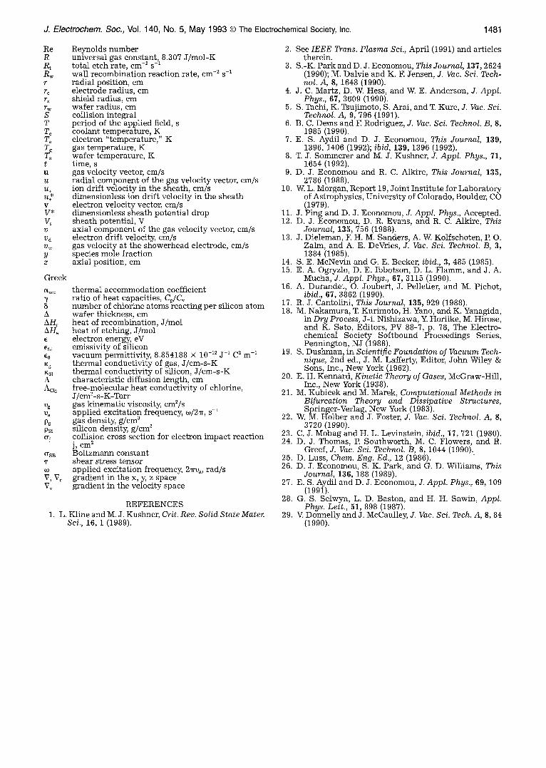
Compar ison of the exper imenta l ly measured e tch ra te w i th the theore t ica l ly predic ted va lue was difficult because there is no kinet ic in format ion on C1 react ions wi th polysi l - icon surfaces in a plasma. Ogryzlo et at. ~5 s tudied the k ine t - ics of polysi l icon e tching wi th C1 atoms in the absence of ion bombardment . In these exper iments , the polysi l icon sample was p laced downs t ream of a plasma. This is in con- t ras t to the present study, where the polysi l icon was ex- posed to the plasma. Despi te this difference, the kinet ic expression repor ted by Ogryzlo et al. (Eq. 27) was used here as a reasonable first approximat ion .
Figure 14 shows the compar i son be tween the exper imen- tal (points) and theore t ica l (lines) e tch ra te at the wafe r center as a funct ion of time. Model predic t ions are shown for two different the rmal accommoda t ion coefficients, c~ .... which was the only ad jus tab le pa rame te r in the model. In order to compare theory to exper iment , the in i t ia t ion pe- r iod requ i red to r emove the oxide (as de te rmined by laser interferometry) was sub t rac ted f rom the real time. The etch ra te is h igher for the lower the rmal accommoda t ion coefficient because the wafe r t empera tu re is then higher. The model captures the ini t ia l t rans ient as wel l as the mag- n i tude of e tch ra te sat isfactor i ly consider ing the uncer- t a in ty in the kinet ic expression used. The increase in etch
1480 J. Electrochem. Soc., Vol. 140, No. 5, May 1993 �9 The Electrochemical Society, Inc.
rate after -120 s cannot be captured by the model in its present form. This increase is due to loading as the poly film is clearing and progressively more of the underlying oxide is exposed to the plasma (the reactivity of C1 on oxide is much lower than that on poly). A rather simple modifi- cation of the model can capture this effect.
It was further found that the model predictions were sen- sitive to the etching reaction activation energy. It appears that better understanding of surface chemistry is impor- tant for enhancing the predictive abilities of the model. In practice, one can adjust the values of the thermal accom- modation, surface recombination, and etching reaction coefficients to fit the experimental data. Such fitting was not attempted here because the use of many adjustable parameters was not desirable.
Summary and Conclusions A comprehensive mathematical model of chlorine etch-
ing of polysilicon in a single-wafer plasma reactor was de- veloped from first principles. A modeling methodology was outlined which can be applied to other plasma systems as well. Solutions to the Boltzmann equation provided the electron transport and reaction coefficients. The glow dis- charge was modeled by dividing the interelectrode space into bulk plasma and sheath. The glow discharge model provided the self-sustaining electric field, electron density and energy, ion bombardment flux and energy, and radical production rate coefficients. The latter were input to neu- tral transport and reaction equations coupled to a wafer heat transport equation. Spatiotemporal variations of etchant concentration, wafer temperature, and etch rate were thus computed.
As a result of the temperature dependence of etch rate, the wafer temperature can have multiple values for the same set of parameters. Under conditions of high etch rate and poor wafer cooling, etching was inherently transient. The energy released by the exothermic etching reaction and back side cooling were found to be the most important en- ergy gain and loss mechanisms, respectively. The situation may be different in high density plasma reactors (e.g., ECR) where ion bombardment can be the main mechanism for wafer heating. The wafer temperature distribution was rel- atively flat except for cases of strongly nonuniform radical concentration profiles across the wafer surface. The shape of the temperature distribution was then found to follow the radical concentration distribution.
The polysilicon etch rate increased with time despite the fact that the atomic chlorine concentration decreased with time. This was due to wafer heating and the Arrhenius de- pendence of etch rate on temperature. Uniformity of etch- ing depended on the relative reactivity (against C1 atoms) of the wafer surface compared to that of the surrounding elec-
3500
3000
.~ 2500
2000
1500
m 1000
5O0
0 0
t
, , , l l l l l , , , l , 1 ] l l i l l l , , l , l l i , l l l l , i
30 60 90 120 150 180
Time (s)
Fig. 14. Comparison of calculated (lines) and measured (points) transients of palysilicon etch rate. Curve a is for ~ = 0.50 and curve b is for C~acc = 0.75. Conditions were 100 W, 0.5 Tarr, and 1.27 cm electrode spacing. Other parameter values as in Table II.
trode surface. A novel technique was developed, based on laser interferometry, to monitor in situ the transients in etch rate and uniformity. Measured etch rate transients compared favorably with model predictions. However, model predictions were sensitive to the surface reaction parameters. Thus, better knowledge of surface kinetics is essential for enhancing the predictive capabilities of the model.
Additional in situ process diagnostics would provide more rigorous tests of the model predictions. For example, laser induced fluorescence (LIF) can provide spatially re- solved atomic chlorine concentration profiles near the wafer surface, 28 where they are needed most. Unfortu- nately, optical emission spectroscopy cannot be used with- in the sheath because there are too few electrons to provide atomic excitation. Besides, the assumptions of actinometry may be violated in the sheath. Also, it would be interesting to monitor the wafer temperature in real time. IR laser interferometry as described by Donnelly and McCaulley 29 appears to be a good choice. One of the main advantages is that this method is nonintrusive. From the practical point of view, however, one is interested in measuring directly the etch rate and its uniformity. The multichannel laser inter- ferometric technique provides a real time monitor of both etch rate and uniformity. Sensors such as this are invalu- able for process control of plasma reactors.
Acknowledgments The authors thank the National Science Foundation
(CBT 8708908), Texas Instruments, Inc., the Welch Founda- tion, and the Texas Advanced Research Program for financial support of this work. We are grateful to Dr. Gabe Barna, Dr. Lee Lowenstein, and Dr. Wayne Fisher of Texas Instruments for providing technical support.
A C Cl C2 CM Csl
D Dae E,E E~ E§ e f /o hB
hr Io L k.
kB ka
ki2 kmn
kr
L me m+ N N~
ne P <Pa~> Q, qo Peh
LIST OF SYMBOLS electrode area, cm 2 species concentration, cm -3 atomic chlorine concentration, cm -3 molecular chlorine concentration, cm -~ concentration of third body, cm -3 surface concentration of atomic chlorine, cm -3 gas heat capacity at constant pressure, J/g-K silicon heat capacity at constant pressure, J/g-K collision number diffusion coefficient, cm2/s electron ambipolar diffusion coefficient, cm2/s electric field, V/em etching reaction activation energy, J/mol ion bombardment energy, eV electronic charge, 1.609 �9 10 -19 C electron velocity distribution function isotropic electron energy distribution function heat transfer coefficient for back side cooling, J/cm2-K-s top-side heat transfer coefficient, J/cm2-K-s peak current, A ion bombardment flux, A/cm 2 dissociative attachment reaction rate constant, em3/s Boltzmann's constant, eV/K molecular chlorine dissociation rate constant, cm3/s atomic chlorine ionization rate constant, cm3/s molecular chlorine ionization rate constant, cm3/s nth order reaction rate constant for a surface material m, cm(3~-2)/s homogeneous (volume) recombination rate constant, cm6/s half interelectrode gap, em electron mass, g ion mass, g total neutral density, cm -3 dopant density, em -3 atom density of silicon, cm -3 electron density, em 3 pressure, Torr time-average RF power, W
3 volumetric flow rate, cm/min, sccm P~clet number for heat transfer
J. Electrochem. Soc., Vol. 140, No. 5, May 1993 �9 The Electrochemical Society, Inc. 1481
R e R Rt Rw r re rs rw S T Tc To
t U U U+ u? V
V* us V
Vd Vw
Y Z
Greek
O~aee "7
A ~xg, zxgo
~Si GO Kg
KSi A Xcl2
1)g ~a Pg Psi O" i
O'SB
O3
V, Vr Vv
Reynolds number universal gas constant, 8.307 J /mol-K total etch rate, cm -2 s -1 wall recombinat ion reaction rate, cm -2 s radia l position, cm electrode radius, cm shield radius, cm wafer radius, cm collision integral per iod of the applied field, s coolant temperature, K electron "temperature," K gas temperature, K wafer temperature, K time, s gas velocity vector, cm/s radial component of the gas velocity vector, cm/s ion drift velocity in the sheath, cm/s dimensionless ion drif t velocity in the sheath electron velocity vector, cm/s dimensionless sheath potent ial drop sheath potential , V axial component of the gas velocity vector, cm/s electron drift velocity, cm/s gas velocity at the showerhead electrode, cm/s species mole fraction axial position, cm
thermal accommodation coefficient ratio of heat capacities, C~/Cv �9 1 ~ . number of chlorine atoms reacting per silicon atom wafer thickness, cm heat of recombination, J/mol heat of etching, J/tool electron energy, eV emissivity of silicon vacuum permittivity, 8.854188 • 10 -12 J-~ C 2 m -1 thermal conductivity of gas, J /cm-s-K thermal conductivity of silicon, J /cm-s-K characterist ic diffusion length, cm free-molecular heat conductivity of chlorine, J/cm2-s-K-Torr gas kinematic viscosity, cm2/s appl ied excitat ion frequency, ~o/2-~, s -1 gas density, g/cm 3 silicon density, g/cm ~ collision cross section for electron impact reaction J, c m 2
Boltzmann constant shear stress tensor appl ied excitat ion frequency, 2~a, rad/s gradient in the x, y, z space gradient in the Velocity space
REFERENCES 1. L. Kline and M. J. Kushner, Crit. Rev. Solid State Mater.
Sci., 16, 1 (1989).
2. See IEEE Trans. Plasma Sci., Apri l (1991) and articles therein.
3. S.-K. Park and D. J. Economou, This Journal, 137, 2624 (1990); M. Dalvie and K. E Jensen, J. Vac. Sci. Tech- nol. A, 8, 1648 (1990).
4. J. C. Martz, D. W. Hess, and W. E. Anderson, J. Appl. Phys., 67, 3609 (1990).
5. S. Tachi, K. Tsujimoto, S. Arai, and T. Kure, J. Vac. Sci. Technol. A, 9, 796 (1991).
6. B. C. Dems and E Rodriguez, J. Vac. Sci. Technol. B, 8, 1985 (1990).
7. E. S. Aydil and D. J. Economou, This Journal, 139, 1396, 1406 (1992); ibid, 139, 1396 (1992).
8. T. J. Sommerer and M. J. Kushner, J. Appl. Phys., 71, 1654 (1992).
9. D. J. Economou and R. C. Alkire, This Journal, 135, 2786 (1988).
10. W. L. Morgan, Report 19, Joint Insti tute for Labora tory of Astrophysics, University of Colorado, Boulder, CO (1979).
11. J. Ping and D. J. Economou, J. Appl. Phys., Accepted. 12. D. J. Economou, D. R. Evans, and R. C. Alkire, This
Journal, 135, 756 (1988). 13. J. Dieleman, F. H. M. Sanders, A. W. Kolfschoten, P. O.
Zalm, and A. E. DeVries, J. Vac. Sci. Technol. B, 3, 1384 (1985).
14. S. E. McNevin and G. E. Becker, ibid., 3,485 (1985). 15. E. A. Ogryzlo, D. E. Ibbotson, D. L. Flamm, and J. A.
Mucha, J. Appl. Phys., 67, 3115 (1990). 16. A. Durandet, O. Joubert, J. Pelletier, and M. Piehot,
ibid., 67, 3862 (1990). 17. R. J. Cantolini, This Journal, 135, 929 (1988). 18. M. Nakamura, T. Kurimoto, H. Yano, and K. Yanagida,
in Dry Process, J-i. Nishizawa, Y. Horiike, M. Hirose, and K. Sato, Editors, PV 88-7, p. 78, The Electro- chemical Society Softbound Proceedings Series, Pennington, NJ (1988).
19. S. Dushman, in Scientific Foundation of Vacuum Tech- nique, 2nd ed., J. M. Lafferty, Editor, John Wiley & Sons, Inc., New York (1962).
20. E. H. Kennard, Kinetic Theory of Gases, McGraw-Hill , Inc., New York (1938).
21. M. Kubicek and M. Marek, Computational Methods in Bifurcation Theory and Dissipative Structures, Springer-Verlag, New York (1983).
22. W. M. Holber and J. Foster, J. Vac. Sci. Technol. A, 8, 3720 (1990).
23. C. J. Mobag and H. L. Levinstein, ibid., 17,721 (1980). 24. D. J. Thomas, P. Southworth, M. C. Flowers, and R.
Greef, J. Vac. Sci. Technol. B, 8, 1044 (1990). 25. D. Luss, Chem. Eng. Ed., 12 (1986). 26. D. J. Economou, S. K. Park, and G. D. Williams, This
Journal, 136, 188 (1989). 27. E. S. Aydil and D. J. Economou, J. Appl. Phys., 69, 109
(1991). 28. G. S. Selwyn, L. D. Baston, and H. H. Sawin, Appl.
Phys. Lett., 51, 898 (1987). 29. V. Donnelly and J. McCaulley, J. Vac. Sci. Tech. A, 8, 84
(1990).


![Journal of Power Sources - WordPress.com · developed electrochemical cell [19]. One pattern per hour was col-lected; the interval between two consecutive XRD patterns corre-sponding](https://static.fdocuments.in/doc/165x107/5f81870a2dc76102f7783b26/journal-of-power-sources-developed-electrochemical-cell-19-one-pattern-per.jpg)


