Modeling of a DAB under phase-shift modulation for design ...
11
HAL Id: hal-03035109 https://hal.archives-ouvertes.fr/hal-03035109 Submitted on 27 Dec 2020 HAL is a multi-disciplinary open access archive for the deposit and dissemination of sci- entific research documents, whether they are pub- lished or not. The documents may come from teaching and research institutions in France or abroad, or from public or private research centers. L’archive ouverte pluridisciplinaire HAL, est destinée au dépôt et à la diffusion de documents scientifiques de niveau recherche, publiés ou non, émanant des établissements d’enseignement et de recherche français ou étrangers, des laboratoires publics ou privés. Modeling of a DAB under phase-shift modulation for design and DM input current filter optimization Glauber de Freitas Lima, Yves Lembeye, Fabien Ndagijimana, Jean-Christophe Crébier To cite this version: Glauber de Freitas Lima, Yves Lembeye, Fabien Ndagijimana, Jean-Christophe Crébier. Modeling of a DAB under phase-shift modulation for design and DM input current filter optimization. 2020 22nd European Conference on Power Electronics and Applications (EPE’20 ECCE Europe), Sep 2020, Lyon, France. pp.P.1-P.10, 10.23919/EPE20ECCEEurope43536.2020.9215851. hal-03035109
Transcript of Modeling of a DAB under phase-shift modulation for design ...

HAL Id: hal-03035109https://hal.archives-ouvertes.fr/hal-03035109
Submitted on 27 Dec 2020
HAL is a multi-disciplinary open accessarchive for the deposit and dissemination of sci-entific research documents, whether they are pub-lished or not. The documents may come fromteaching and research institutions in France orabroad, or from public or private research centers.
L’archive ouverte pluridisciplinaire HAL, estdestinée au dépôt et à la diffusion de documentsscientifiques de niveau recherche, publiés ou non,émanant des établissements d’enseignement et derecherche français ou étrangers, des laboratoirespublics ou privés.
Modeling of a DAB under phase-shift modulation fordesign and DM input current filter optimization
Glauber de Freitas Lima, Yves Lembeye, Fabien Ndagijimana,Jean-Christophe Crébier
To cite this version:Glauber de Freitas Lima, Yves Lembeye, Fabien Ndagijimana, Jean-Christophe Crébier. Modelingof a DAB under phase-shift modulation for design and DM input current filter optimization. 202022nd European Conference on Power Electronics and Applications (EPE’20 ECCE Europe), Sep 2020,Lyon, France. pp.P.1-P.10, �10.23919/EPE20ECCEEurope43536.2020.9215851�. �hal-03035109�

Modeling of a DAB under phase-shift modulation for design and DM input current filter optimization
Glauber de Freitas Lima, Yves Lembeye. Fabien Ndagijimana and Jean-Christophe Crebier
Univ. Grenoble Alpes, CNRS, Grenoble INP, G2Elab, F-38000 Grenoble, France E-Mail: [email protected] [email protected]
inp.fr [email protected] [email protected]
URL: https://g2elab.grenoble-inp.fr/
Acknowledgements
This research work has been supported by an Auvergne Rhone Alpes FEDER funding for Mamaatec Project in partnership with MAATEL company, located in Moirans, France.
Keywords
«EMC/EMI», «Harmonics», «High frequency power converter», «Optimization», « Passive filter»
Abstract
This paper investigates the conducted Differential Mode Current (DMC) harmonic magnitudes and the Power Factor (PF) produced by a Dual Active Bridge (DAB) converter operated under single phase-shift modulation. Power factor and the first harmonic are modeled and analyzed though a dimensionless plane of static gain versus output parametrized current. It is shown that voltage and output current ranges have a significant impact on the magnitude of the reactive power and DMC filter needs, which can therefore compromise the performance of the DAB. Especially, the DMC should be considered in the DAB converter design optimization to avoid EMI filter oversizing or non-compliance with respect to EMC standards.
Introduction
Some of the future and trends of power electronic systems consists of multi-objective optimization designs such as power density, overall or peak efficiency, technology and economic viability [1]. Looking for best performance over large output voltage and/or current ranges while keeping high efficiency and power density requires a comprehensive mathematical modeling. For a power electronic converter, as presented in [2], assuring optimum power density while keeping high efficiency for the entire range of power is a challenging work as there is always a compromise between power density and efficiency. Therefore, analyzing the converter over a frame of operating points: static gain, input and output voltages and currents are fundamental for design optimization.
Particularly, it is known that the design of a DAB under phase-shift modulation requires a careful choice of the phase-shift, switching frequency and ac link inductance regarding reactive power [3], ZVS operation [4] and high-efficiency. Commonly, in the literature, these issues are usually treated with respect to output power [4], [5], making the analysis more specific to a single design. Besides output power information does not differentiate low voltage and high current from high voltage and low current applications. As it is demonstrated through the paper, for a DAB converter, even at same output power operating points, getting the input and output voltage and current information is essential to analyze its performance characteristics. Similar to [6], the plane of the static gain versus an output parametrized current will be used for the sake of a generic, dimensionless and still meaningful analysis. It is presented the modeling in the frequency domain of the input DMC normalized current of a lossless DAB, in such a way that the performance characteristic of power factor and DMC normalized harmonic impacts can be observed through this suitable plane. As it is presented a lossless theory, the power factor will represent the notion of efficiency, as the amount of reactive power impacts on both the efficiency [7]

and the power density, whereas the first harmonic appearing in the lower limit of the frequency spectrum represent the effort for filtering to comply with regulations. Therefore, both analysis of power factor and DMC first harmonic represent how much the converter in a general way (filter, isolation, cooling, and etc.) should be oversized for a given output voltage and current operating ranges. Giving the desired input voltage, output voltage and current ranges, the designer will be able to find an optimum design with respect to different parameters as well as to identify the critical regions and limitations found in a DAB. To overcome these natural limitations or to enhance its performance and keeping same or similar converter topology, different strategies can be implemented, such as different dual phase-shift modulation [8], variable-tap transformer [9], frequency modulation [10] or even a combination of phase-shift and frequency modulation [11].
Besides proposing a guideline to design a DAB and to characterize its performance, the methodology proposed here can be used for other any converter in which analysis can be done using the same or similar output parametrized current [12], [13]. The dimensionless analysis therefore allows actual comparison among different power converters where tradeoffs become clearer to observe.
The assumptions made about the DAB presented throughout this paper are the following: • The DAB is operated with classical single phase-shift modulation [14];
• The input voltage is assumed to be a constant voltage source;
• Only steady state operation is considered;
• Non-idealities such as propagation delays, dead-times [15], series parasitic resistances [16], magnetic and switching losses [17], [18] are not modeled;
• The ac link capacitance is considered to be infinite and its effect [19] is neglected;
• The magnetizing inductance is considered to be infinite and its effect [6] is also neglected
• Profile charge (light load and heavy load) has equal importance for all operating points;
• Even though bidirectional, only unidirectional power flow analysis are depicted;
• A simple lossless theoretical analysis is presented, and therefore, it does not allow finding separately the optimum switching frequency fs and ac link inductance Lac, but rather its product fsLac.
Dual Active Bridge DMC Modeling in the Frequency Domain
The main waveforms of the DAB converter when operated under phase shift control are recalled. Fig. 1 (a) shows the topology of the DAB converter and the main voltage and current waveforms under phase-shift operation. Voltage waveforms correspond to AC squared voltages produced by the two H-bridges and applied on the input and output sides of the AC link. A generic input current of the DAB is described in Fig. 1 (b).
(a) (b) Fig. 1: (a) Ideal electrical equivalent circuit of a DAB; (b) Main time domain waveforms of a DAB. In order to present an analysis that is generic, dimensionless and independent of the load resistance, a parametrization of the output current is presented in (1). The reconstruction of the input current in the time domain can then be normalized as presented in (4)-(7).

2 s AC o
i
f L I
rV = (1)
o
i
rVM
V= (2)
180d
= (3)
Where:
• Vi is the input voltage (V);
• Vo is the output voltage (V);
• Io is the average output current (A);
• fs is the switching frequency (Hz);
• Lac is the AC link inductance (H);
• α is the phase-shift in degrees from 0° to 180°;
• r is the transformer turns ratio.
( )( ) ( ), , 1
, ,in
in
o
I M d Md dI M d
I r
−= = (4)
( )( ) ( ), , 1 2 1
, ,2
a
a
o
I M d M dI M d
I r
− −= = (5)
( )( ), , 2 1
, ,2
b
b
o
I M d M dI M d
I r
+ −= = (6)
( )
( ) ( )( )
( )( )
( )
1
2
, , 2 1+ , , 0
2, , ,
2 1 ( ), , 2 1
+ , , 2 2
s
a
o sin
so
sb
o s s
i M d f M t dI M d t
I r fi M d t
df M tI
i M d f dI M d t
I r f f
+=
=− −
=
(7)
Where:
• t is the time (s). Applying Fourier series theory, the DM input current can be described in the frequency domain. The normalized coefficients are shown in (8), (9) and the reconstruction of the normalized input current, back to the time domain is then presented in (10). Notice that the frequency of the input current corresponds in theory to the double of the switching frequency as illustrated in Fig. 1 (b). Finally, it is presented the normalized values of the input harmonic current in (11). From it, the RMS value of the DMC and power factor are developed as presented in (12) and (13), respectively.
( )( ) ( )
2
2 2
, , 2sin, , ,
n
n
o
a M d dn Ma M d n
I n r
= = − (8)
( )( ) ( )
2 2
, , sin 2 2, , ,
n
n
o
b M d M dn M n M dn nb M d n
I n r
+ − −= = (9)
( )( ) ( ) ( ) ( ) ( )( )
1
, , , , ,, , , , , cos 4 , , , sin 4Fourrierin s
in n s n s
no
i M d n f tI M d a M d n nf t b M d n nf t
I
=
= + + (10)
Where:
• n is the harmonic order;
( )( ) ( ) ( )
2 2, , , , , , , , ,
, , ,2
in
in
n n n
n
o
H M d n a M d n b M d nH M d n
I
+= =
(11)
( )( )
( ) ( )( )2
2
1
, ,, , , , , ,RMS
RMS in
in
in in n
no
I M dI M d I M d H M d
I
=
= = + (12)
( )( )
( )
,Pf ,
,RMS
in
in
I M dM d
I M d= (13)
The value of the phase-shift is not as significant, since in current controlled applications the feedback control imposes the desired phase-shift value. Therefore, knowing that the parametrized output current is given as in (14), the value of the phase-shift in equations (4) to (13) so far presented is substituted as a function of the parametrized current presented in (15). Besides, from now on the Power factor and DMC first harmonic analysis become dependent on only two variables: M and γ. Notice that two
different values of the phase-shift are possible for the same output parametrized current. The domain of the phase-shit is comprehended from 0° to 180° for delivering power. However, it is known that there are no benefits in operating with phase-shit larger than 90° [3], that is d larger than 0.5.
( )1d d = − (14)
1 1 4 1 1 4
2 2d
− − −= (15)
As d is a real number, it can be shown that the parametrized output current has a maximum value limited by 0.25, shown in (16). This shows that the possible values of the product fsLac are limited as presented in (17).
1
4 (16)
8
is ac
o
rVf L
I (17)
As in [3], a necessary condition for achieving ZVS in the first and second H-bridges is that the currents
𝐼𝑎 and 𝐼𝑏 to be larger than zero, respectively. Considering (15), ZVS conditions in the first and second H-bridges follow as presented in (18) and (19), respectively.
1 if 1
1 4M M
−
(18)
1 4 if 1M M − (19)
Power factor and DMC first harmonic analysis
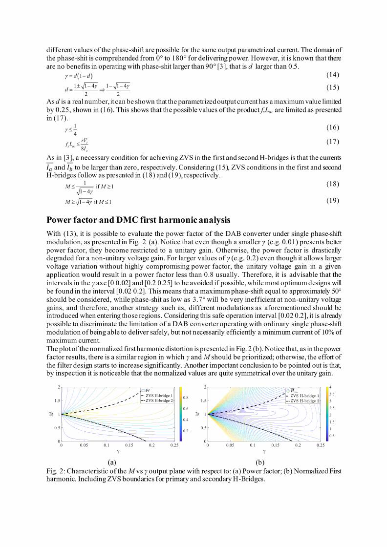
With (13), it is possible to evaluate the power factor of the DAB converter under single phase-shift modulation, as presented in Fig. 2 (a). Notice that even though a smaller γ (e.g. 0.01) presents better power factor, they become restricted to a unitary gain. Otherwise, the power factor is drastically degraded for a non-unitary voltage gain. For larger values of γ (e.g. 0.2) even though it allows larger voltage variation without highly compromising power factor, the unitary voltage gain in a given application would result in a power factor less than 0.8 usually. Therefore, it is advisable that the intervals in the γ axe [0 0.02] and [0.2 0.25] to be avoided if possible, while most optimum designs will be found in the interval [0.02 0.2]. This means that a maximum phase-shift equal to approximately 50° should be considered, while phase-shit as low as 3.7° will be very inefficient at non-unitary voltage gains, and therefore, another strategy such as, different modulations as aforementioned should be introduced when entering those regions. Considering this safe operation interval [0.02 0.2], it is already possible to discriminate the limitation of a DAB converter operating with ordinary single phase-shift modulation of being able to deliver safely, but not necessarily efficiently a minimum current of 10% of maximum current. The plot of the normalized first harmonic distortion is presented in Fig. 2 (b). Notice that, as in the power factor results, there is a similar region in which γ and M should be prioritized; otherwise, the effort of the filter design starts to increase significantly. Another important conclusion to be pointed out is that, by inspection it is noticeable that the normalized values are quite symmetrical over the unitary gain.
(a) (b) Fig. 2: Characteristic of the M vs γ output plane with respect to: (a) Power factor; (b) Normalized First harmonic. Including ZVS boundaries for primary and secondary H-Bridges.

Parametrized output load plane
The analysis of the power factor and first harmonic will be observed over the parametrized output plane shown in Fig. 2. On it, it will be placed a rectangular region formed by the intervals [Mo Mf] (y axe) and [γo γf ] (x axe) as presented in Fig 3 (a). The domain in which the output parametrized current will operate is directly related to the percentage of minimum output current allowed, as presented in (20). Therefore, from (16), the maximum value of γo as a function of Io% is presented in (21). For convenience, the parameter Mo% is defined in (22).
%o o fI = (20)
%
4
oo
I (21)
%o f oM M M= − (22)
Where:
• Mo is the minimum static gain desired;
• Mf is the maximum static gain desired; • γo is the initial parametrized output current;
• γf is the initial parametrized output current;
• Io% is the minimum current desired in percentage of the rated current;
• Mo% is output voltage variation in percentage.
(a) (b)
Fig. 3: Characteristic of the output plane M vs γ for Mo% = 0.4 and Io% = 0.5 with respect to: (a) Power factor (one single design); (b) Normalized DMC first harmonic (different designs). Then, the power factor and the first harmonic contained in this region will be analyzed and discussed further. It is important to know that, depending on the choice of the parameters, this rectangular region
can be wider or not, and not symmetrical over the unitary gain. For example, γ varying [0.1 0.2] and M
varying [0.8 1.2] allows minimum load of 50% of rated current and 40% of voltage variation, while γ varying [0.05 0.1] and M varying [1.4 1.8] allows the same 50% and 40% of variation, as presented in Fig. 2 (b), even though the area of the later region on the output plane is halved and shifted on the plane. A direct consequence from it is that a smaller γo allows designing a converter capable of delivering more range of output current variation more easily than larger ones. However, it should be noted that direct consequences with respect to ZVS region, power factor and first harmonic should be taken into account. The parametrized plane underlines important observations in a straightforward way. For example:
• Since same output power can be expressed for different values of M, Io and Vi, it is important to differentiate each scenario as they can result in completely different power factor or harmonic distortion;
• Besides, still considering same output power, high input voltage and low output current applications will necessarily require an increase of the product fsLac to keep the same performance of low input voltage and high output current applications;
• To maintain the same power factor and DMC harmonics (i.e. to keep the same performance) insensitive to input voltage variations, a simple frequency modulation proportional to the input voltage variation appears to be very suitable.

Characterization and performance optimization of the DAB converter
As it can be seen for a given output current variation Io% and voltage gain variation Mo% there is a set of
[γo γf] and [Mo Mf], to be chosen that will result in an optimized design either with respect to power factor and / or first harmonic distortion. In this paper, a charge profile is related to this rectangular frame, but any other one, with different geometric formats, such as a battery charger could be analyzed and optimized through the presented methodology.
Power factor evaluation
To cover the entire rectangular region, a parameter Pfvol is proposed as the integration in volume of the power factor divided by the volume of a cube that contains such region, as presented in (23) and depicted in Fig. 4 (a). By sweeping the values of Mo and γf for Io% = 0.5 and Mo% = 0.4, it is possible to notice that there is a global maximum at Mo = 0.922 and γf = 0.148, resulting in Pfvol = 0.9 as presented in Fig. 4 (b). However, considering that the gain is around the unitary gain, e.g. Mo = 0.8 and Mo = 1.2, equation (23) is adapted into (24), and it is observed a maximum point at γf = 0.128, resulting in Pfvol = 0.88. An important conclusion is that these values mean that the turns ratio r can be used as an optimizing variable to produce such gains, and that symmetry over the unitary gain does not necessarily brings the best results with respect to this parameter Pfvol.
( )( )
( )
%
%
% %
Pf , d d
Pf , if 0 0.251
o o f
o f o
M M
M I
vol o f f
o f o
M M
MM I
+
= −
(23)
( )( )
( )
%
%%
12
12
%
% %
Pf , d d
P.f , if 0 0.251
of
of o
M
MI
vol o f f
o f o
M M
MM I
+
−
= −
(24)
Fig. 4: (a) The volume of the power factor over a given range in the output plane; (b) The results of the parameter defined in (23) for Io% = 0.5 and Mo% = 0.4. Nevertheless, still considering this symmetry over the unitary static gain as in (24), for each Mo% varying from 0 to 1 and Io% varying from 0 to 1, it is possible to take the optimum γf that will deliver the maximum value of Pfvol, as presented in in (25) and depicted in Fig. 5 (a). For every optimum γf (25), and substituting its value in (24), it is possible to observe the results with respect to Pf vol in which plot results is presented in Fig. 5 (b).
(a) (b) Fig. 5: (a) Values of γf (25) that results in the maximum value of the parameter Pf vol for both Mo% and Io% varying from 0 to 1; (b) Maximum value of Pf vol considering (25).

( )( )
( )
%
%%
12
12
% %
% %
Pf , d d
, if 0 0.251
of
of o
M
MI
f o o f
f o f o
M Md
M I rootd M I
+
−
= −
(25)
Besides providing an optimization process, these plots show the natural limitation found in a DAB converter with simple phase-shit modulation regarding voltage and current range extension. Again, to overcome these issues, different techniques should be performed when entering in critical areas.
DMC first harmonic evaluation
From Fig. 6 (a), it is possible to realize that the worst-case normalized values are always located in the
extreme coordinates (Mo, γo), (Mo, γf), (Mf, γo) and (Mf, γf). In order to identify more precisely, the first harmonic is verified for each voltage gain as presented in Fig 6 (a). Notice that, considering voltage variation over the unitary gain, the step-down mode results in equal or larger values than the step-up mode. For example, among the static gains varying from 0.8 to 1.2, the value of 0.8 is the one that results the highest value. Considering M = 0.8, the value of γ that returns the least value for first harmonic is
0.138 resulting in 𝐻1𝑖𝑛= 0.45. Once the value of γf has been chosen, the parameter in (26) allows to
identify the consequences of decreasing current variation Io%, at a given voltage gain M. In Fig. 6 (b), it is presented the plot results of (26) for M = 0.8 and a set of different γf.
( ) ( )1 % % 1 %, , ,1 , ,1in inf o o f oH M I I H M I = (26)
(a) (b) Fig. 6: (a) The value of the normalized DMC first harmonic for different static gains; (b) The effect of decreasing current for M = 0.8 and different γf . It is possible to demonstrate that lower currents will never affect more than the maximum designed current, and therefore, the filter design shall be designed considering the rated current as well as its worst voltage gain scenario, that is (Mo, γf). By inspection, notice that there is an interval where most γf should be designed contained in the interval from 0.1 to 0.2. Indeed, in this interval, the normalized DMC first harmonic is quite constant, especially for M = 0.8.
DMC filter design
In this section, it is assumed that the frequency of the first harmonic will be larger than 150 kHz, that is, the lower limit of frequency band defined by CISPR class A and B. Therefore, if lower switching frequencies than 75 kHz are applied, it is necessary to consider the next highest harmonic order n larger than 150 kHz in the equations so far presented. Equation (11) will be brought to its absolute value and transformed into dBµV in 50 Ω system for better visualization when designing the filter to meet CISPR emission limits, as presented in (27). The filter should be calculated for its worst-case condition, e.g. Mo
= 0.8. Then, it should be chosen the value of γf, e.g., 0.14 resulting in 𝐻1𝑖𝑛= 0.45 as presented in previous
section. Finally, the filter becomes a function of the attenuation required to comply with the EMC standards, approximately 60 dBµV, as presented in (28). As an example, Io = 5 A, Mo = 0.8 and γf = 0.14 results in an attenuation required of about 100 dB. Then, as in [2], the attenuation value is used to calculate the filter that could be e.g., 1- or 2- LC filter structures, as depicted in Fig. 7 (a). The compromise of choosing each structure is related to the cutoff

frequency and its required total realization effort, as shown in Fig. 7 (b). In general, higher filter orders enable designing a filter with a higher cutoff frequency, resulting in structures with smaller total volume. However, a careful study regarding parasitic resonances and loss effects in a filter should be taken into account for the sake of precisely optimization.
( ) ( )( ) ( ) ( )1
6
1, ,1 20log , ,1 20log 10 20log 50inin
H o odB V M H M I = + + (27)
( )1
Filter , ,1 60in
att H odB V M dB V = − (28)
(a) (b) Fig. 7: (a) An example of filter design with 1 - or 2 - LC structures; (b) Filter attenuation per decade and the cutoff frequency for 1- and 2 - LC structures.
Considering careful designs, the value of 𝐻1𝑖𝑛can be roughly be approximate as worst cases equal to
one, as in db such value does not impact more than 6 db if even deviated by twice as much the real value. This also means that the output current is the one that interferes the most in the filtering design.
Practical results
A DAB converter, designed for low voltage and power applications [20], [21], [22] (10 V to 20 V and 100 W) presented in Fig. 8 (a), was used to conduct practical results with respect to power factor. Considering its AC link inductor of 700 nH, an output current of 3 A and 1.5 A and input voltage of 10 V, the switching frequency were calculated as 330 kHz, in such a way that the parameter γf is set at 0.14 and γo is at 0.07. In Fig. 7 (b) it is presented the waveform of current measured in the AC link when Io = 1.5 A and Mo= 0.8 in which ideally presents the same RMS value of the input current. Once the average values of the input and output currents are measured, it is possible to derive the power factor and efficiency of the converter, as presented in Table I.
(a) (b) Fig. 8: (a) Low voltage and power DAB used for practical results; (b) Waveform of the current in the AC link inductor (light blue color) for Io = 1.5 A and Mo = 0.8.
Table I: Practical results
Io = 1.5 A
Mo = 0.8
Io = 1.5 A
Mo = 1.2
Io = 3.0 A
Mo = 0.8
Io = 3.0 A
Mo = 1.2
Iin (A) 1.38 1.2 2.15 1.8 2.91 2.4 4.4 3.6
ILac_RMS (A) 1.78 1.88 2.68 2.14 3.51 3.27 4.95 3.92
(Degree°) 10.40 13.44 20.70 13.44 33.60 29.83 41.40 29.83

Pf 0.78 0.64 0.80 0.84 0.83 0.73 0.89 0.92
Efficiency (%) 85.8 100 84.7 100 83.1 100 81.1 100
At each operating point, it is presented both the practical and theoretical results of the lossless modeling here proposed for comparison purposed. The difference between theoretical and practical results is clearly related to AC series resistance, since voltage drop across this AC resistance sums up with the needed output voltage. This will cause a shifting in the static gain in such a way that step-down modes will approach the unitary gains improving its features, while step-up modes will move up further away, harming its characteristics. This means that, due to AC resistance and other non-idealities, the power factor and harmonics might present different results from the lossless theory. Nonetheless, it is possible to notice that indeed the step-up mode presented better results than the step-down mode with respect to power factor, whereas with respect to efficiency, step-down modes presented better results. This shows that power factor and efficiency does not maintain a proportional or linear relation. Besides, regarding error between practical and theoretical results, non-idealities seems to effect more deeply low phase-shift intervals than high phase-shift ones. Therefore, a modeling accounting for at least AC series resistance is crucial for the performance characterization and design optimization of the DAB.
Conclusion
The methodology here proposed can be used to easily characterize in a generic way the performance of a DAB converter operating with sing phase-shift modulation; to optimize, identify or limit voltage and current ranges with respect to power factor parameters and DMC filter needs. Straightforward and meaningful converter design and optimization can be carried out with the parametrized plane, as the consequences of varying input voltage, static gain, output current, switching frequency and transformer turns ratio; and how those variable effects the performance of the DAB converter becomes well visible. Similar analysis could be performed in another converter topology. Besides, since dimensionless investigation is performed, actual comparison among different converter could be a possibility. In this paper, the rectangular region is placed without weighting the importance of the current values. Therefore, it is suggested the developing of new parameters to consider such factor. As before mentioned, the charge profile, of a given application e.g., battery charger can be used over the output plane for optimization purposes. As it could be noticed, a lossless theory does not allow identification of the parameter fsLac separately nor does the efficiency, while large errors of matching theoretical with practical results are susceptible. Therefore, future studies include the AC series resistive, parallel transformer and commutation losses as well as filter losses and parasitic, in such a way that the parameter of efficiency can be well analyzed in the same way as with power factor and harmonic distortion. At the end, for future studies, it is expected to have a methodology where any given optimum criteria can be evaluated: overall efficiency in a given output voltage and current ranges (profile charge), power density and EMC compliance.
References
[1] J. W. Kolar, J. Biela, S. Waffler, T. Friedli and U. Badstuebner.: Performance trends and limitations of power
electronic systems, 2010 6th International Conference on Integrated Power Electronics Systems, Nuremberg, 2010,
pp. 1-20.
[2] J. W. Kolar, F. Krismer, Y. Lobsiger, J. Muhlethaler, T. Nussbaumer and J. Minibock .: Extreme efficiency
power electronics, 2012 7th International Conference on Integrated Power Electronics Systems (CIPS),
Nuremberg, 2012, pp. 1-22.
[3] A. R. Rodríguez Alonso, J. Sebastian, D. G. Lamar, M. M. Hernando and A. Vazquez .: An overall study of a
Dual Active Bridge for bidirectional DC/DC conversion, 2010 IEEE Energy Conversion Congress and Exposition,
Atlanta, GA, 2010, pp. 1129-1135, doi: 10.1109/ECCE.2010.5617847.

[4] A. Rodríguez, A. Vázquez, D. G. Lamar, M. M. Hernando and J. Sebastián .: Different Purpose Design
Strategies and Techniques to Improve the Performance of a Dual Active Bridge With Phase-Shift Control, in IEEE
Transactions on Power Electronics, vol. 30, no. 2, pp. 790-804, Feb. 2015, doi: 10.1109/TPEL.2014.2309853.
[5] D. Costinett, R. Zane and D. Maksimovic.: Automatic voltage and dead time control for efficiency optimization
in a Dual Active Bridge converter, 2012 Twenty-Seventh Annual IEEE Applied Power Electronics Conference
and Exposition (APEC), Orlando, FL, 2012, pp. 1104-1111, doi: 10.1109/APEC.2012.6165956.
[6] M. N. Kheraluwala, R. W. Gascoigne, D. M. Divan and E. D. Baumann.: Performance characterization of a
high-power dual active bridge DC-to-DC converter, in IEEE Transactions on Industry Applications, vol. 28, no.
6, pp. 1294-1301, Nov.-Dec. 1992, doi: 10.1109/28.175280.
[7] J. Wu, P. Wen, X. Sun and X. Yan.: Reactive Power Optimization Control for Bidirectional Dual-Tank
Resonant DC–DC Converters for Fuel Cells Systems, in IEEE Transactions on Power Electronics, vol. 35, no. 9,
pp. 9202-9214, Sept. 2020, doi: 10.1109/TPEL.2020.2971733.
[8] X. Liu et al..: Novel Dual-Phase-Shift Control With Bidirectional Inner Phase Shifts for a Dual-Active-Bridge
Converter Having Low Surge Current and Stable Power Control, in IEEE Transactions on Power Electronics, vol.
32, no. 5, pp. 4095-4106, May 2017, doi: 10.1109/TPEL.2016.2593939.
[9] A. Jafari, M. S. Nikoo, F. Karakaya and E. Matioli.: Enhanced DAB for Efficiency Preservation Using
Adjustable-Tap High-Frequency Transformer, in IEEE Transactions on Power Electronics, vol. 35, no. 7, pp.
6673-6677, July 2020, doi: 10.1109/TPEL.2019.2958632.
[10] J. Hiltunen, V. Väisänen, R. Juntunen and P. Silventoinen.: Variable-Frequency Phase Shift Modulation of a
Dual Active Bridge Converter, in IEEE Transactions on Power Electronics, vol. 30, no. 12, pp. 7138 -7148, Dec.
2015, doi: 10.1109/TPEL.2015.2390913.
[11] F. Jauch and J. Biela .: Combined Phase-Shift and Frequency Modulation of a Dual-Active-Bridge AC–DC
Converter With PFC, in IEEE Transactions on Power Electronics, vol. 31, no. 12, pp. 8387 -8397, Dec. 2016, doi:
10.1109/TPEL.2016.2515850.
[12] A. J. B. Bottion and I. Barbi.: A family of three-level DC-DC converters, 2013 Brazilian Power Electronics
Conference, Gramado, 2013, pp. 115-122, doi: 10.1109/COBEP.2013.6785103.
[13] M. Gatti Bottarelli, I. Barbi, Y. Romulo De Novaes and A. Rufer.: Three-level quadratic non-insulated basic
DC-DC converters, 2007 European Conference on Power Electronics and Applications, Aalborg, 2007, pp. 1 -10,
doi: 10.1109/EPE.2007.4417584.
[14] B. Zhao, Q. Song, W. Liu and Y. Sun, "Overview of Dual-Active-Bridge Isolated Bidirectional DC–DC
Converter for High-Frequency-Link Power-Conversion System," in IEEE Transactions on Power Electronics, vol.
29, no. 8, pp. 4091-4106, Aug. 2014, doi: 10.1109/TPEL.2013.2289913.
[15] B. Zhao, Q. Song, W. Liu and Y. Sun.: Dead-Time Effect of the High-Frequency Isolated Bidirectional Full-
Bridge DC–DC Converter: Comprehensive Theoretical Analysis and Experimental Verification, in IEEE
Transactions on Power Electronics, vol. 29, no. 4, pp. 1667-1680, April 2014, doi: 10.1109/TPEL.2013.2271511.
[16] I. Aghabali, L. Dorn-Gomba, P. Malysz and A. Emadi.: Parasitic Resistance Effect on Dual Active Bridge
Converter, IECON 2019 - 45th Annual Conference of the IEEE Industrial Electronics Society, Lisbon, Portugal,
2019, pp. 1932-1937, doi: 10.1109/IECON.2019.8926896.
[17] K. Zhang, Z. Shan and J. Jatskevich.: Estimating switching loss and core loss in dual active bridge DC-DC
converters, 2015 IEEE 16th Workshop on Control and Modeling for Power Electronics (COMPEL), Vancouver,
BC, 2015, pp. 1-6, doi: 10.1109/COMPEL.2015.7236501.
[18] F. Krismer and J. W. Kolar.: Accurate Power Loss Model Derivation of a High-Current Dual Active Bridge
Converter for an Automotive Application, in IEEE Transactions on Industrial Electronics, vol. 57, no. 3, pp. 881 -
891, March 2010, doi: 10.1109/TIE.2009.2025284.
[19] R. Lenke, F. Mura and R. W. De Doncker.: Comparison of non-resonant and super-resonant dual-active ZVS-
operated high-power DC-DC converters, 2009 13th European Conference on Power Electronics and Applications,
Barcelona, 2009, pp. 1-10.
[20] Crebier, J.-C.; Phung, T.-H.; Nguyen, V.-S.; Lamorelle, T.; Andreta, A.; Kẻachev, L.; Lembeye, Y.: DC-AC
Isolated Power Converter Array. Focus on Differential Mode Conducted EMI, Electronics 2019, 8, 999.
[21] T. Lamorelle, Y. Lembeye and J. Crébier.: Handling Differential Mode Conducted EMC in Modular
Converters, in IEEE Transactions on Power Electronics, vol. 35, no. 6, pp. 5812 -5819, June 2020, doi:
10.1109/TPEL.2019.2947735.
[22] T. Lamorelle, S. Nguyen, J. C. Podvin, D. Rubio, Y. Lembeye and J. Crebier.: Multi-cell DC-DC converters
- Input differential mode filtering generic design rules and implementation, PCIM Europe 2019; International
Exhibition and Conference for Power Electronics, Intelligent Motion, Renewable Energy and Energy
Management, Nuremberg, Germany, 2019, pp. 1-8.