modeling and simulation of pv array with boost converter
56
MODELING AND SIMULATION OF PV ARRAY WITH BOOST CONVERTER: AN OPEN LOOP STUDY A THESIS IN PARTIAL FULFILMENTS OF REQUIREMENTS FOR THE AWARD OF THE DEGREE OF Bachelor of Technology Submitted to NATIONAL INSTITUTE OF TECHNOLOGY, ROURKELA BY DEPARTMENT OF ELECTRICAL ENGINEERING NATIONAL INSTITUTE OF TECHNOLOGY ROURKELA – 769008 INDIA 2011 DEBASHIS DAS 107EE024 SHISHIR KUMAR PRADHAN 107EE039
Transcript of modeling and simulation of pv array with boost converter
MODELING AND SIMULATION OF PV
ARRAY WITH BOOST CONVERTER: AN
OPEN LOOP STUDY
A THESIS IN PARTIAL FULFILMENTS OF REQUIREMENTS
FOR THE AWARD OF THE DEGREE OF
Bachelor of Technology
Submitted to
NATIONAL INSTITUTE OF TECHNOLOGY, ROURKELA
BY
DEPARTMENT OF ELECTRICAL ENGINEERING
NATIONAL INSTITUTE OF TECHNOLOGY
ROURKELA – 769008
INDIA
2011
DEBASHIS DAS
107EE024
SHISHIR KUMAR PRADHAN
107EE039

ii
MODELING AND SIMULATION OF PV ARRAY
WITH BOOST CONVERTER: AN OPEN LOOP
STUDY
A THESIS IN PARTIAL FULFILMENTS OF REQUIREMENTS
FOR THE AWARD OF THE DEGREE OF
Bachelor of Technology
Submitted to
NATIONAL INSTITUTE OF TECHNOLOGY, ROURKELA
BY
Under the supervision of
PROF. SOMNATH MAITY
DEPARTMENT OF ELECTRICAL ENGINEERING
NATIONAL INSTITUTE OF TECHNOLOGY
ROURKELA – 769008
INDIA
2011
DEBASHIS DAS
107EE024
SHISHIR KUMAR PRADHAN
107EE039

iii
NATIONAL INSTITUTE OF TECHNOLOGY
ROURKELA
CERTIFICATE
This is to certify that the thesis entitled “Modeling and simulation of PV array with boost
converter : An open loop study” submitted by Debashis Das (107EE024) and Shishir Kumar
Pradhan (107EE039) in the partial fulfillment of the requirements for the award of Bachelor of
Technology degree in Electrical Engineering at National Institute of Technology, Rourkela is an
authentic work carried out by them under my supervision and guidance.
To the best of my knowledge, the matter embodied in the thesis has not been submitted to any
other University/Institute for the award of any Degree or Diploma.
Date: Prof. Somnath Maity
Dept. of Electrical Engineering
NIT Rourkela

iv
ACKNOWLEDGEMENT
We wish to express our deep sense of gratitude and indebtedness to Prof. SOMNATH MAITY,
Department of Electrical Engineering, N.I.T Rourkela, for introducing the present topic and for
their inspiring guidance, constructive criticism and valuable suggestion throughout this project
work.
Our sincere thanks to all our friends who have patiently extended all sorts of help for
accomplishing this undertaking.
Date: DEBASHIS DAS (107EE024)
Place: SHISHIR KUMAR PRADHAN (107EE039)
Department of Electrical Engineering
National Institute of Technology
Rourkela - 769008

v
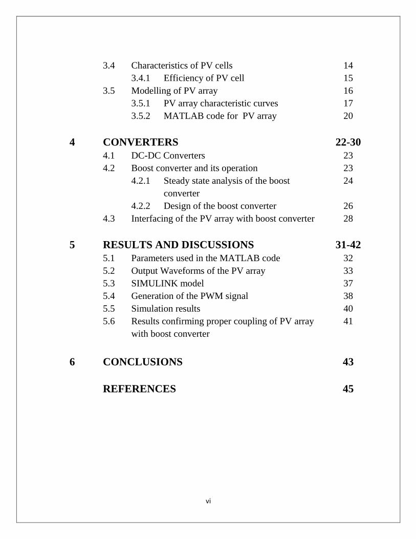
CONTENTS
CHAPTER TITLE PAGE
Certificate iii
Acknowledgement iv
Contents v
List of tables vii
List of figures viii
ABSTARCT 1
1 INTRODUCTION 2-3
1.1 Motivation 3
1.2 Work summary 3
2 PRELIMINARIES 4-9
2.1 Renewable energy 5
2.2 Solar energy 5
2.3 Distribution of solar radiation 6
2.4 Solar radiation reaching earth surface 7
2.5 Spectrum of sun 8
2.6 Standard test conditions (STC) 9
3 PHOTOVOLTAIC SYSTEMS 10-21
3.1 Definition 11
3.2 Photovoltaic arrangements 11
3.2.1 Photovoltaic cell 11
3.2.2 Photovoltaic module 12
3.2.3 Photovoltaic array 12
3.3 Materials used in PV cells 13
vi
3.4 Characteristics of PV cells 14
3.4.1 Efficiency of PV cell 15
3.5 Modelling of PV array 16
3.5.1 PV array characteristic curves 17
3.5.2 MATLAB code for PV array 20
4 CONVERTERS 22-30
4.1 DC-DC Converters 23
4.2 Boost converter and its operation 23
4.2.1 Steady state analysis of the boost
converter
24
4.2.2 Design of the boost converter 26
4.3 Interfacing of the PV array with boost converter 28
5 RESULTS AND DISCUSSIONS 31-42
5.1 Parameters used in the MATLAB code 32
5.2 Output Waveforms of the PV array 33
5.3 SIMULINK model 37
5.4 Generation of the PWM signal 38
5.5 Simulation results 40
5.6 Results confirming proper coupling of PV array
with boost converter
41
6 CONCLUSIONS 43
REFERENCES 45

vii
LIST OF TABLES
TABLE
NO. TITLE
PAGE
NO.
1. Parameters value used in MATLAB code 32
2. Value of input voltage and current for variation in load resistance for
an irradiance level (100 mW/m2)
41
3.
Value of input voltage and current for variation in load resistance for
an irradiance level (80 mW/m2)
42
viii
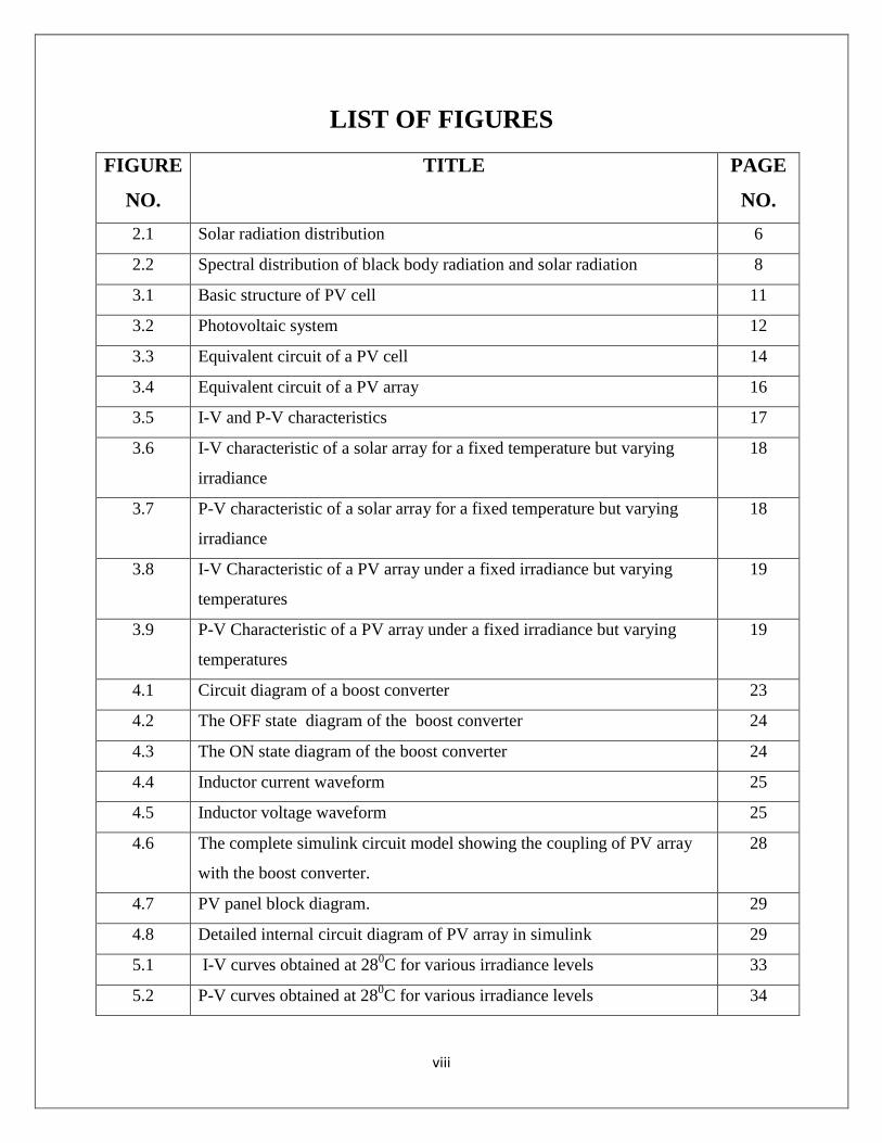
LIST OF FIGURES
FIGURE
NO.
TITLE PAGE
NO.
2.1 Solar radiation distribution 6
2.2 Spectral distribution of black body radiation and solar radiation 8
3.1 Basic structure of PV cell 11
3.2 Photovoltaic system 12
3.3 Equivalent circuit of a PV cell 14
3.4 Equivalent circuit of a PV array 16
3.5 I-V and P-V characteristics 17
3.6 I-V characteristic of a solar array for a fixed temperature but varying
irradiance
18
3.7 P-V characteristic of a solar array for a fixed temperature but varying
irradiance
18
3.8 I-V Characteristic of a PV array under a fixed irradiance but varying
temperatures
19
3.9 P-V Characteristic of a PV array under a fixed irradiance but varying
temperatures
19
4.1 Circuit diagram of a boost converter 23
4.2 The OFF state diagram of the boost converter 24
4.3 The ON state diagram of the boost converter 24
4.4 Inductor current waveform 25
4.5 Inductor voltage waveform 25
4.6 The complete simulink circuit model showing the coupling of PV array
with the boost converter.
28
4.7 PV panel block diagram. 29
4.8 Detailed internal circuit diagram of PV array in simulink 29
5.1 I-V curves obtained at 280C for various irradiance levels 33
5.2 P-V curves obtained at 280C for various irradiance levels 34

ix
5.3 P-I curves obtained at 280C for various irradiance levels 34
5.4 I-V curves obtained at an irradiance of 100 mW /cm2 for various
temperatures
35
5.5 P-I curves obtained at an irradiance of 100 mW/cm2 for various
temperatures.
35
5.6 P-V curves obtained at an irradiance of 100 mW/cm2 various
temperatures.
36
5.7 The complete simulation model of the PV energy conversion system. 37
5.8 Circuit diagram for PWM signal generation 38
5.9 Simulation diagram showing the generation of the PWM signal 38
5.10 PWM signal generated 39
5.11 The current output of the system 40
5.12 The voltage output of the system 40
5.13 Interfacing of PV array simulation result with open loop I-V
characteristic
42
P a g e | 1
ABSTRACT
The recent upsurge in the demand of PV systems is due to the fact that they produce electric
power without hampering the environment by directly converting the solar radiation into electric
power. However the solar radiation never remains constant. It keeps on varying throughout the
day. The need of the hour is to deliver a constant voltage to the grid irrespective of the variation
in temperatures and solar insolation. We have designed a circuit such that it delivers constant and
stepped up dc voltage to the load. We have studied the open loop characteristics of the PV array
with variation in temperature and irradiation levels. Then we coupled the PV array with the boost
converter in such a way that with variation in load, the varying input current and voltage to the
converter follows the open circuit characteristic of the PV array closely. At various insolation
levels, the load is varied and the corresponding variation in the input voltage and current to the
boost converter is noted. It is noted that the changing input voltage and current follows the open
circuit characteristics of the PV array closely.

Chapter 1
INTRODUCTION

P a g e | 3
1.1 MOTIVATION The Conventional sources of energy are rapidly depleting. Moreover the cost of energy is
rising and therefore photovoltaic system is a promising alternative. They are abundant, pollution
free, distributed throughout the earth and recyclable. The hindrance factor is it’s high installation
cost and low conversion efficiency. Therefore our aim is to increase the efficiency and power
output of the system. It is also required that constant voltage be supplied to the load irrespective
of the variation in solar irradiance and temperature. PV arrays consist of parallel and series
combination of PV cells that are used to generate electrical power depending upon the
atmospheric conditions (e.g solar irradiation and temperature). So it is necessary to couple the
PV array with a boost converter. Moreover our system is designed in such a way that with
variation in load, the change in input voltage and power fed into the converter follows the open
circuit characteristics of the PV array. Our system can be used to supply constant stepped up
voltage to dc loads.
1.2 WORK SUMMARY
We have discussed about the renewable energy, solar energy, distribution of solar
radiation reaching the earth’s surface and spectrum of sun in chapter 2. The details regarding the
PV cell have been discussed in chapter 3. The PV array has been designed in MATLAB
environment. The open-circuit characteristic of the PV cell has been studied in depth. The boost
converter design, the coupling of the PV array with the converter has been described in chapter
4. The chapter 5 deals with the simulation results and discussions part. The P-V, I-V, P-I curves
have been obtained at varying irradiation levels and temperatures. The generation of the PWM
signal has been shown. We get constant voltage across the load resistance of the boost converter.
Output load of the boost converter is varied and the variation in the input voltage and current fed
into the boost converter is noted. The various values of the voltage and current have been plotted
in the open loop curves of the PV array. The voltage and current values lie on the curves and
thereby prove that our coupling of the boost converter with the PV array is proper.

Chapter 2
PRELIMINARIES

P a g e | 5
2.1 RENEWABLE ENERGY
Renewable energy sources also called non-conventional type of energy are the sources
which are continuously replenished by natural processes. Such as, solar energy, bio-energy -
bio-fuels grown sustainably, wind energy and hydropower etc., are some of the examples of
renewable energy sources. A renewable energy system convert the energy found in sunlight,
falling-water, wind, sea-waves, geothermal heat, or biomass into a form, which we can use in
the form of heat or electricity. The majority of the renewable energy comes either directly or
indirectly from sun and wind and can never be fatigued, and therefore they are called renewable
[12].
However, the majority of the world's energy sources came from conventional sources-
fossil fuels such as coal, natural gases and oil. These fuels are often term non-renewable energy
sources. Though, the available amount of these fuels are extremely large, but due to decrease in
level of fossil fuel and oil level day by day after a few years it will end. Hence renewable energy
source demand increases as it is environmental friendly and pollution free which reduces the
greenhouse effect [12].
2.2 SOLAR ENERGY
Solar energy is a non-conventional type of energy. Solar energy has been harnessed by
humans since ancient times using a variety of technologies. Solar radiation, along with secondary
solar-powered resources such as wave and wind power, hydroelectricity and biomass, account
for most of the available non-conventional type of energy on earth. Only a small fraction of the
available solar energy is used [13].
Solar powered electrical generation relies on photovoltaic system and heat engines. Solar
energy's uses are limited only by human creativity. To harvest the solar energy, the most
common way is to use photo voltaic panels which will receive photon energy from sun and
convert to electrical energy. Solar technologies are broadly classified as either passive
solar or active solar depending on the way they detain, convert and distribute solar energy.

P a g e | 6
Active solar techniques include the use of PV panels and solar thermal collectors to strap up the
energy. Passive solar techniques include orienting a building to the Sun, selecting materials with
favorable thermal mass or light dispersing properties and design spaces that naturally circulate
air [5].Solar energy has a vast area of application such as electricity generation for distribution,
heating water, lightening building, crop drying etc.
2.3 DISTRIBUTION OF SOLAR RADIATION
Figure 2.1 Solar radiation distribution [18].
From the above Figure 2.1 of solar radiation, Earth receives 174 petawatts (PW) of
incoming solar radiation at the upper atmosphere. Approximately 30% is reflected back to space
and only 89 pw is absorbed by oceans and land masses. The spectrum of solar light at the Earth's
surface is generally spread across the visible and near-infrared reason with a small part in
the near-ultraviolet. The total solar energy absorbed by Earth's atmosphere, oceans and land
masses is approximately 3,850,000 EJ per year [13].

P a g e | 7
2.4 SOLAR RADIATION REACHING EARTH SURFACE
The intensity of solar radiation reaching earth surface which is 1369 watts per square
meter is known as Solar Constant. It is important to realize that it is not the intensity per square
meter of the Earth’s surface but per square meter on a sphere with the radius of 149,596,000 km
and with the Sun at its centre.
The total amount solar radiation intercepted by the Earth is the Solar Constant multiplied
by the cross section area of the Earth. If we now divide the calculated number by the surface area
of the Earth, we shall find how much solar radiation is received in an average per square meter of
the Earth's surface [10]. Hence the average solar radiation R per square meter of the Earth
surface is,
where S is the solar constant (1369
), r is the earth radius.
The Handy formula which is used to calculate solar energy received by earth
E=3.6* )*S*n*
where E is the solar energy in EJ.
S is the Solar Constant in W/m2.
n is the number of hours.
r is the Earth's radius in km [10].

P a g e | 8
2.5 SPECTRUM OF SUN
The performance of Photovoltaic device is reliant on the spectral distribution of solar
radiation. The standard spectral distribution is mainly used as reference for evaluation of PV devices.
There are two standard terrestrial distribution defined by the American Society for Testing and
Materials (ASTM), global AM1.5 and direct normal. The solar radiation that is perpendicular to a
plane directly facing the sun is known as direct normal. The global corresponds to the spectrum of
the diffuse radiations. Diffuse radiations are the radiations which are reflected on earth’s surface or
influenced by atmospheric conditions. To measure the global radiations an instrument named
pyranometer is used. This instrument is designed in such a way that it responds to each wavelengths
and so that we get a precise value for total power in any incident spectrum [5].
Figure 2.2 Spectral distribution of black body radiation and sun radiation [11].
The AM initials in the above Figure stands for air mass. The air mass in this circumstance means
the mass of air between a surface and the sun [6]. The length of the path of solar radiation from
the sun through the atmosphere is indicated by the number AMx. The longer the path the more is
the deviation of light. The AM0 in the above figure means the spectral distribution and intensity
of sunlight in near-earth space without atmospheric attenuation [6].

P a g e | 9
2.6 STANDARD TEST CONDITIONS (STC)
The comparison between different photovoltaic cells can be done on the basis of there
performance and characteristic curve. The parameters are always given in datasheet. The
datasheet make available the notable parameter regarding the characteristics and performance of
PV cells with respect to standard test condition.
Standard test conditions are as follows:
Temperature (Tn) = 250c
Irradiance (Gn) = 1000
Spectrum of x = 1.5 i.e. AM.

Chapter 3
PHOTOVOLTAIC
SYSTEMS
P a g e | 11
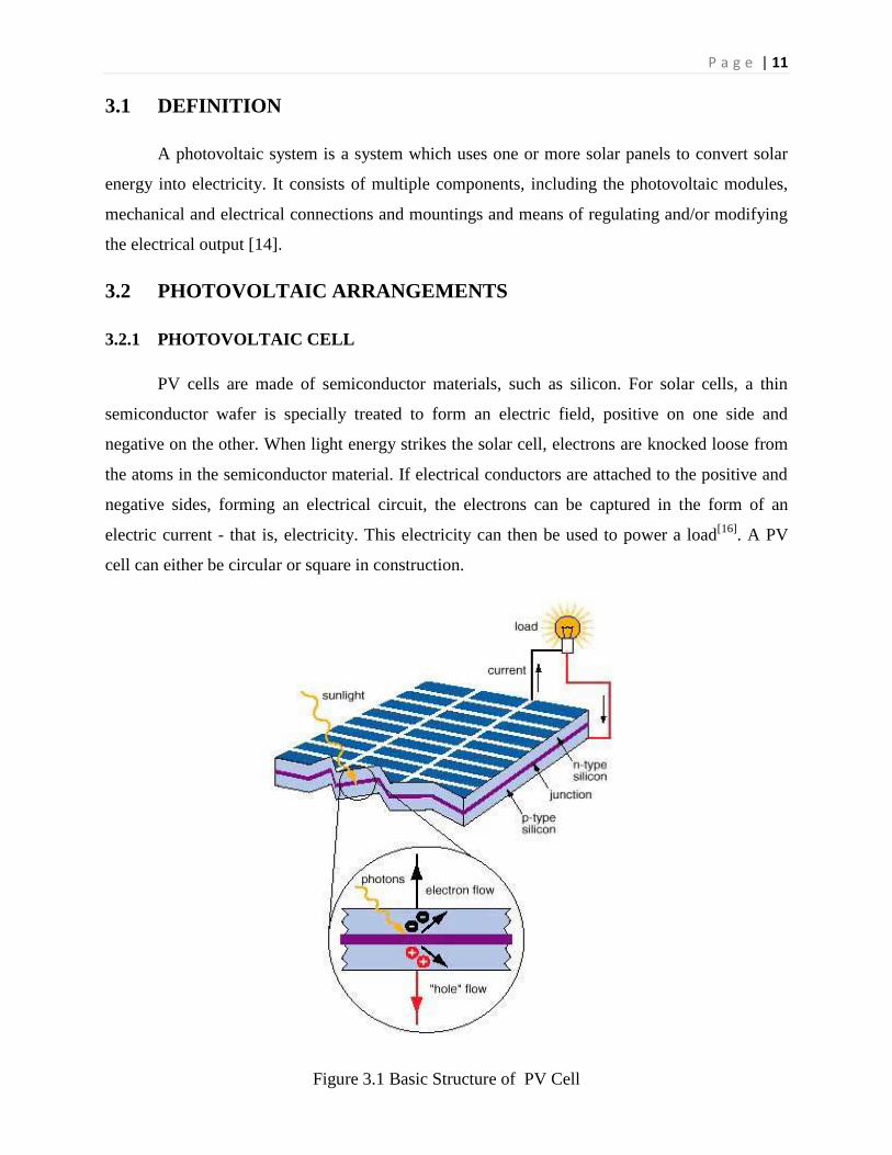
3.1 DEFINITION
A photovoltaic system is a system which uses one or more solar panels to convert solar
energy into electricity. It consists of multiple components, including the photovoltaic modules,
mechanical and electrical connections and mountings and means of regulating and/or modifying
the electrical output [14].
3.2 PHOTOVOLTAIC ARRANGEMENTS
3.2.1 PHOTOVOLTAIC CELL
PV cells are made of semiconductor materials, such as silicon. For solar cells, a thin
semiconductor wafer is specially treated to form an electric field, positive on one side and
negative on the other. When light energy strikes the solar cell, electrons are knocked loose from
the atoms in the semiconductor material. If electrical conductors are attached to the positive and
negative sides, forming an electrical circuit, the electrons can be captured in the form of an
electric current - that is, electricity. This electricity can then be used to power a load[16]
. A PV
cell can either be circular or square in construction.
Figure 3.1 Basic Structure of PV Cell

P a g e | 12
3.2.2 PHOTOVOLTAIC MODULE
Due to the low voltage generated in a PV cell (around 0.5V), several PV cells are
connected in series (for high voltage) and in parallel(for high current) to form a PV module for
desired output. Separate diodes may be needed to avoid reverse currents, in case of partial or
total shading, and at night. The p-n junctions of mono-crystalline silicon cells may have adequate
reverse current characteristics and these are not necessary. Reverse currents waste power and can
also lead to overheating of shaded cells. Solar cells become less efficient at higher temperatures
and installers try to provide good ventilation behind solar panels [15].
3.2.3 PHOTOVOLTAIC ARRAY
The power that one module can produce is not sufficient to meet the requirements of
home or business. Most PV arrays use an inverter to convert the DC power into alternating
current that can power the motors, loads, lights etc. The modules in a PV array are usually first
connected in series to obtain the desired voltages; the individual modules are then connected in
parallel to allow the system to produce more current [14].
Figure 3.2 Photovoltaic system [16]

P a g e | 13
3.3 MATERIALS USED IN PV CELL
The materials used in PV cells are as follows:
Single-crystal silicon
Single-crystal silicon cells are the most common in the PV industry. The main technique for
producing single-crystal silicon is the Czochralski (CZ) method. High-purity polycrystalline is
melted in a quartz crucible. A single-crystal silicon seed is dipped into this molten mass of
polycrystalline. As the seed is pulled slowly from the melt, a single-crystal ingot is formed. The
ingots are then sawed into thin wafers about 200-400 micrometers thick (1 micrometer =
1/1,000,000 meter). The thin wafers are then polished, doped, coated, interconnected and
assembled into modules and arrays [7].
Polycrystalline silicon
Consisting of small grains of single-crystal silicon, polycrystalline PV cells are less energy
efficient than single-crystalline silicon PV cells. The grain boundaries in polycrystalline silicon
hinder the flow of electrons and reduce the power output of the cell. A common approach to
produce polycrystalline silicon PV cells is to slice thin wafers from blocks of cast polycrystalline
silicon. Another more advanced approach is the “ribbon growth” method in which silicon is
grown directly as thin ribbons or sheets with the approach thickness for making PV cells [7].
Gallium Arsenide (GaAs)
A compound semiconductor made of two elements: Gallium (Ga) and Arsenic (As). GaAs has a
crystal structure similar to that of silicon. An advantage of GaAs is that it has high level of light
absorptivity. To absorb the same amount of sunlight, GaAs requires only a layer of few
micrometers thick while crystalline silicon requires a wafer of about 200-300 micrometers thick.
Also, GaAs has much higher energy conversion efficiency than crystal silicon, reaching about 25
to 30%.The only drawback of GaAs PV cells is the high cost of single crystal substrate that
GaAs is grown on [7].
Cadmium Telluride (CdTe)
It is a polycrystalline compound made of cadmium and telluride with a high light absorbility
capacity (i.e a small thin layer of the compound can absorb 90% of solar irradiation).The main
P a g e | 14
disadvantage of this compound is that the instability of PV cell or module performance. As it a
toxic substance, the manufacturing process should be done by extra precaution [7].
Copper Indium Diselenide (CuInSe2)
It is a polycrystalline compound semiconductor made of copper, indium and selenium. It delivers
high energy conversion efficiency without suffering from outdoor degradation problem. It is one
of the most light-absorbent semiconductors. As it is a complex material and toxic in nature so the
manufacturing process face some problem [7].
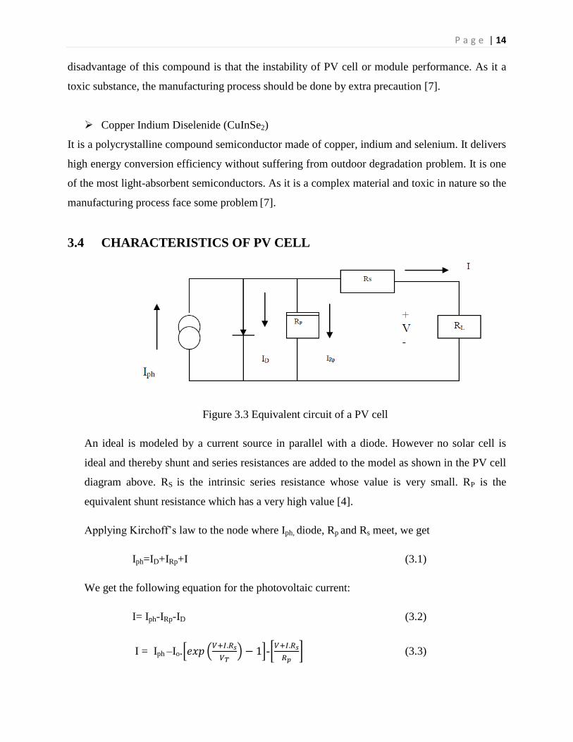
3.4 CHARACTERISTICS OF PV CELL
Figure 3.3 Equivalent circuit of a PV cell
An ideal is modeled by a current source in parallel with a diode. However no solar cell is
ideal and thereby shunt and series resistances are added to the model as shown in the PV cell
diagram above. RS is the intrinsic series resistance whose value is very small. RP is the
equivalent shunt resistance which has a very high value [4].
Applying Kirchoff’s law to the node where Iph, diode, Rp and Rs meet, we get
Iph=ID+IRp+I (3.1)
We get the following equation for the photovoltaic current:
I= Iph-IRp-ID (3.2)
I = Iph –Io.* (
) +-[
] (3.3)

P a g e | 15
Where, Iph is the Insolation current, I is the Cell current, I0 is the Reverse saturation
current, V is the Cell voltage, Rs is the Series resistance, Rp is the Parallel resistance, VT is the
Thermal voltage (
), K is the Boltzman constant, T is the Temperature in Kelvin, q is the
Charge of an electron.
3.4.1 EFFICIENCY OF PV CELL
The efficiency of a PV cell is defined as the ratio of peak power to input solar power.
η=
(
) (3.4)
where, Vmp is the voltage at peak power, Imp is the current at peak power, I is the solar intensity
per square metre, A is the area on which solar radiation fall.
The efficiency will be maximum if we track the maximum power from the PV system at
different environmental condition such as solar irradiance and temperature by using different
methods for maximum power point tracking.

P a g e | 16
3.5 MODELLING OF PV ARRAY:
The building block of PV arrays is the solar cell, which is basically a p-n junction that
directly converts light energy into electricity: it has a equivalent circuit as shown below in Figure
3.4.
Figure 3.4 Equivalent circuit of a PV cell
The current source Iph represents the cell photo current; Rj is used to represent the non-linear
impedence of the p-n junction; Rsh and Rs are used to represent the intrinsic series and shunt
resistance of the cell respectively. Usually the value of Rsh is very large and that of Rs is very
small,hence they may be neglected to simplify the analysis. PV cells are grouped in larger units
called PV modules which are further interconnected in series-parallel configuration to form PV
arrays or PV generators[3]
.The PV mathematical model used to simplify our PV array is
represented by the equation:
I=npIph-npIrs[exp(
*
) -1] (3.5)
where I is the PV array output current; V is the PV array output voltage; ns is the number of cells
in series and np is the number of cells in parallel; q is the charge of an electron; k is the
Boltzmann’s constant; A is the p-n junction ideality factor; T is the cell temperature (K); Irs is the
cell reverse saturation current. The factor A in equation (3.5) determines the cell deviation from
the ideal p-n junction characteristics; it ranges between 1-5 but for our case A=2.46 [3].
The cell reverse saturation current Irs varies with temperature according to the following
equation:
Irs=Irr[
]
3exp(
[
-
]) (3.6)

P a g e | 17
Where Tr is the cell reference temperature, Irr is the cell reverse saturation temperature at Tr and
EG is the band gap of the semiconductor used in the cell.
The temperature dependence of the energy gap of the semi conductor is given by [20]:
EG= EG(0)-
(3.7)
The photo current Iph depends on the solar radiation and cell temperature as follows:
Iph=[ Iscr + Ki(T – Tr)]
(3.8)
where Iscr is the cell short-circuit current at reference temperature and radiation, Ki is the short
circuit current temperature coefficient, and S is the solar radiation in mW/cm2. The PV power
can be calculated using equation (3.5) as follows:
P=IV= npIphV[(
*
)-1] (3.9)
3.5.1 PV ARRAY CHARACTERISTIC CURVES
The current to voltage characteristic of a solar array is non-linear, which makes it
difficult to determine the MPP. The Figure below gives the characteristic I-V and P-V curve for
fixed level of solar irradiation and temperature.
Figure 3.5 I-V and PV curve characteristics [19].
P a g e | 18
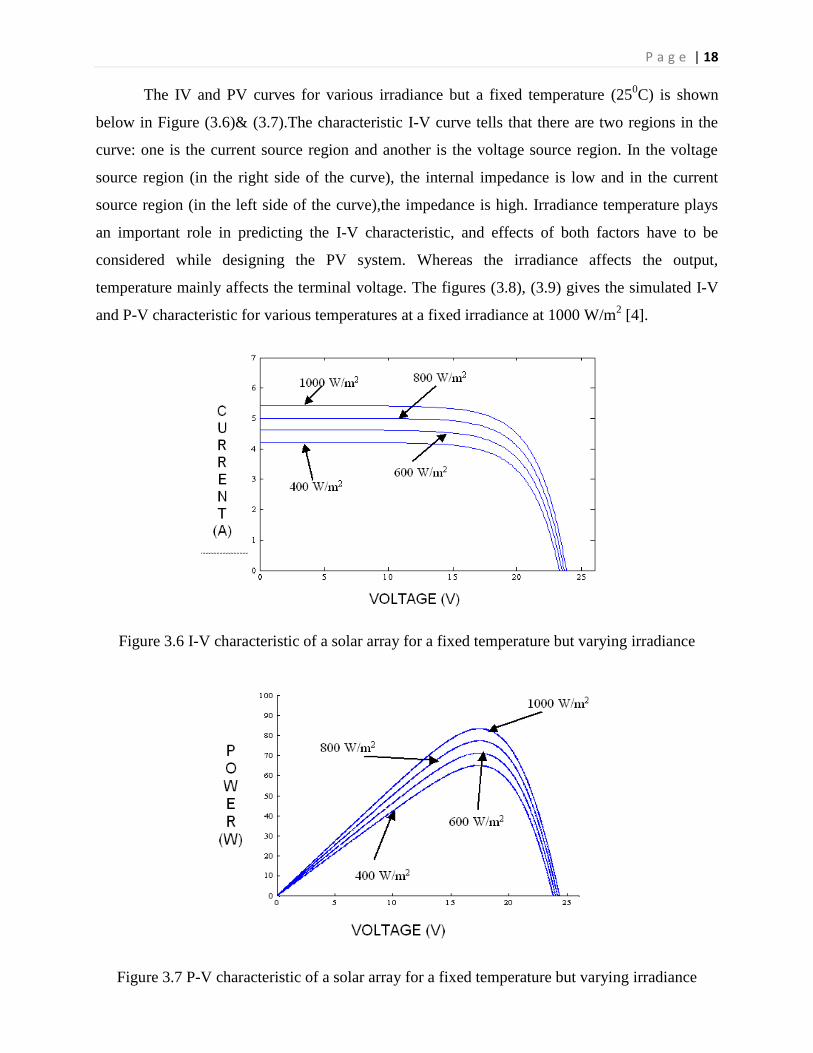
The IV and PV curves for various irradiance but a fixed temperature (250C) is shown
below in Figure (3.6)& (3.7).The characteristic I-V curve tells that there are two regions in the
curve: one is the current source region and another is the voltage source region. In the voltage
source region (in the right side of the curve), the internal impedance is low and in the current
source region (in the left side of the curve),the impedance is high. Irradiance temperature plays
an important role in predicting the I-V characteristic, and effects of both factors have to be
considered while designing the PV system. Whereas the irradiance affects the output,
temperature mainly affects the terminal voltage. The figures (3.8), (3.9) gives the simulated I-V
and P-V characteristic for various temperatures at a fixed irradiance at 1000 W/m2 [4].
Figure 3.6 I-V characteristic of a solar array for a fixed temperature but varying irradiance
Figure 3.7 P-V characteristic of a solar array for a fixed temperature but varying irradiance

P a g e | 19
Figure 3.8 I-V Characteristic of a PV array under a fixed irradiance but varying temperatures
Figure 3.9 P-V Characteristic of a PV array under a fixed irradiance but varying temperatures.
From the I-V, we observe that the short circuit current increases with increase in
irradiance at a fixed temperature. Moreover, from the I-V and P-V curves at a fixed irradiance, it
is observed that the open circuit voltage decreases with increase in temperature.

P a g e | 20
3.5.2 MATLAB CODE FOR PV ARRAY
T=28+273;
Tr1=40; % Reference temperature in degree fahrenheit
Tr=((Tr1-32)*
)+273; % Reference temperature in kelvin
S=[100 80 60 40 20]; % Solar radiation in mW/sq.cm
%S=70;
ki=0.00023; % in A/K
Iscr=3.75; % SC Current at ref. temp. in A
Irr=0.000021; % in A
k=1.38065*10^(-23); % Boltzmann constant
q=1.6022*10^(-19); % charge of an electron
A=2.15;
Eg(0)=1.166;
alpha=0.473;
beta=636;
Eg=Eg0-(alpha*T*T)/(T+beta)*q; % band gap energy of
semiconductor used
cell in joules
Np=4;
Ns=60;
V0=[0:1:300];
for i=1:5
Iph=(Iscr+ki*(T-Tr))*((S(i))/100);
Irs=Irr*((T/Tr)^3)*exp(q*Eg/(k*A)*((1/Tr)-(1/T)));
I0=Np*Iph-Np*Irs*(exp(q/(k*T*A)*V0./Ns)-1);
P0 = V0.*I0;
figure(1)
plot(V0,I0);
axis([0 50 0 20]);
xlabel('Voltage in volt');
ylabel('Current in amp');
hold on;
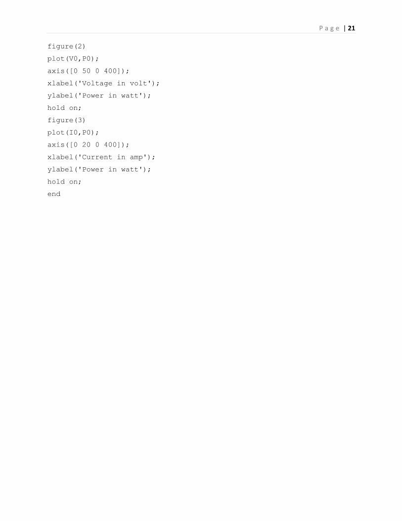
P a g e | 21
figure(2)
plot(V0,P0);
axis([0 50 0 400]);
xlabel('Voltage in volt');
ylabel('Power in watt');
hold on;
figure(3)
plot(I0,P0);
axis([0 20 0 400]);
xlabel('Current in amp');
ylabel('Power in watt');
hold on;
end
Chapter 4
CONVERTERS
P a g e | 23
4.1 DC-DC CONVERTERS
DC-DC converters can be used as switching mode regulators to convert an unregulated
dc voltage to a regulated dc output voltage. The regulation is normally achieved by PWM at a
fixed frequency and the switching device is generally BJT, MOSFET or IGBT. The minimum
oscillator frequency should be about 100 times longer than the transistor switching time to
maximize efficiency. This limitation is due to the switching loss in the transistor. The transistor
switching loss increases with the switching frequency and thereby, the efficiency decreases. The
core loss of the inductors limits the high frequency operation. Control voltage Vc is obtained by
comparing the output voltage with its desired value. Then the output voltage can be compared
with its desired value to obtain the contol voltage Vcr. The PWM control signal for the dc
converter is generated by comparing Vcr with a sawtooth voltage Vr.[8]. There are four
topologies for the switching regulators: buck converter, boost converter, buck-boost converter,
cứk converter. However my project work deals with the boost regulator and further discussions
will be concentrated towards this one.
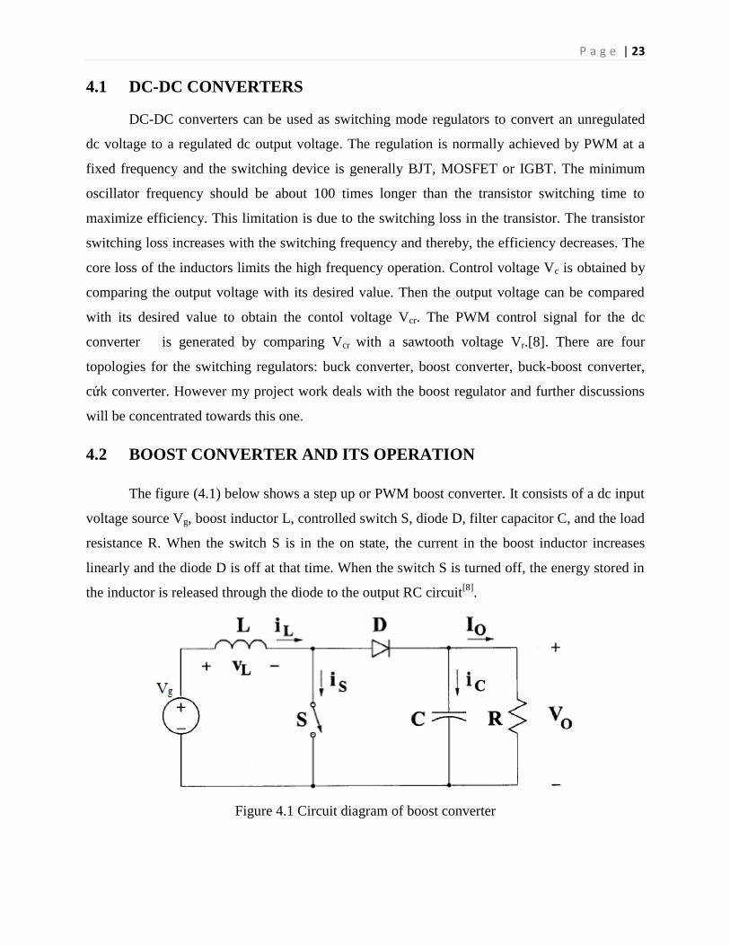
4.2 BOOST CONVERTER AND ITS OPERATION
The figure (4.1) below shows a step up or PWM boost converter. It consists of a dc input
voltage source Vg, boost inductor L, controlled switch S, diode D, filter capacitor C, and the load
resistance R. When the switch S is in the on state, the current in the boost inductor increases
linearly and the diode D is off at that time. When the switch S is turned off, the energy stored in
the inductor is released through the diode to the output RC circuit[8]
.
Figure 4.1 Circuit diagram of boost converter

P a g e | 24
4.2.1 STEADY STATE ANALYSIS OF THE BOOST CONVERTER
(a) OFF STATE:
In the OFF state, the circuit becomes as shown in the Figure (4.2) below [9].
Figure 4.2 The OFF state diagram of the boost converter
When the switch is off, the sum total of inductor voltage and input voltage appear as the load
voltage.
(b) ON STATE:
In the ON state, the circuit diagram is as shown below in Figure (4.3):
Figure 4.3 The ON state diagram of the boost converter
When the switch is ON, the inductor is charged from the input voltage source Vg and the
capacitor discharges across the load. The duty cycle, D=
where T=

P a g e | 25
Figure 4.5 Inductor voltage waveform
Figure 4.4 Inductor current waveform
From the inductor voltage balance equation, we have:-
Vg(DTs) +(Vs-Vo)(1-D)Ts=0
Vg(DTs)-Vg(DTs)-VgTs+VoDTs-VoTs=0
Vo=Vg/(1-D)
Conversion ratio, M=Vo/Vg=1/(1-D) (4.1)
From inductor current ripple analysis, change in inductor current,
Il=(Imax-Imin)
IL=(Vg/L)*(DTs)
IL = (VgD)/(fsL)
L=VgD/fs( IL) (4.2)
The boost converter operates in CCM (continuous conducting mode) for L> Lb where
Lb=
(4.3)
The current supplied to the output RC circuit is discontinuous. Thus a large filter capacitor is
used to limit the output voltage ripple. The filter capacitor must provide the output dc current to
the load when the diode D is off.

P a g e | 26
The minimum value of the filter capacitance that results in the voltage ripple Vr[8]
is given by:
Cmin=
(4.4)
4.2.2 DESIGN OF THE BOOST CONVERTER
(1) CURRENT RIPPLE FACTOR (CRF):
According to IEC harmonics standard, CRP should be bounded within 30%.
i.e
= 30% (4.5)
(2) VOLTAGE RIPPLE FACTOR (VRF):
i.e
= 5% (4.6)
(3) SWITCHING FREQUENCY (fs):
Fs= 100 KHz (4.7)
GIVEN DATA:
Input voltage, Vg=25V
Output voltage, Vo=300V
Output load current, Io=1A
Step 1 : Calculation of Duty cycle (D):
=
=

P a g e | 27
D=11/12=.9166 (4.8)
Step 2: Calculation of Ripple Current :
IL= 1 A
=(0.3 * 1)A=0.3 A (4.9)
Step 3: Calculation of Inductor value (L):
L = (
) = (25*.9166)/(0.3 *10^5) = 7.63 * 10^ -4 H. (4.10)
Step 4: Calculation of capacitor value(C) :
We have,
=
(4.11)
R0 =
= 300/1= 300. (4.12)
C=D/f * R0 *( V0/V)= (.9166)/(10^5)*(300)*(.05)= .611 µF. (4.13)
The transfer function of the boost converter[12] used for the modeling is given by:
G(s) =
(4.14)
Putting the values of R, L, C, D, Vg in the above equation, the transfer equation that results is
given by:
G(s ) =
(4.15)
By trial and error, we get the value of KP which gives desired results as 6.03.

P a g e | 28
4.3 INTERFACING OF THE PV ARRAY WITH BOOST CONVERTER
The PV array has been interfaced with the boost converter using a controlled voltage source as
shown in the circuit diagram below:
Figure 4.6 The complete simulink circuit model showing the coupling of PV array with the boost
converter
P a g e | 29
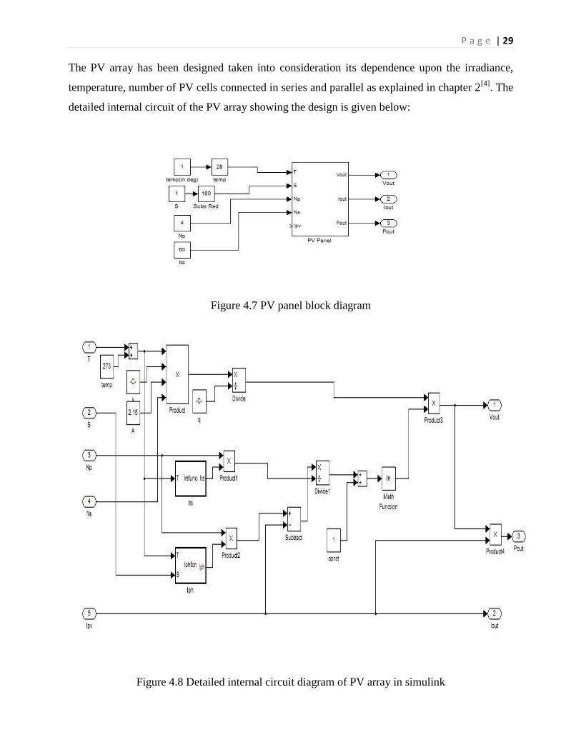
The PV array has been designed taken into consideration its dependence upon the irradiance,
temperature, number of PV cells connected in series and parallel as explained in chapter 2[4]
. The
detailed internal circuit of the PV array showing the design is given below:
Figure 4.7 PV panel block diagram
Figure 4.8 Detailed internal circuit diagram of PV array in simulink

P a g e | 30
The M-file for Irs function has been developed using the equation (3.6) and that for the Iph
function using equation (3.8). The PV array has been modeled using the equations (3.1) – (3.9).
The interfacing of the PV array with the boost converter has been achieved using a voltage
controlled source. The inductor current which is same as the load current of the PV system is
used as feedback for designing the PV array.

Chapter 5
RESULTS AND
DISCUSSIONS

P a g e | 32
5.1 PARAMETERS USED IN THE MATLAB CODE
The values of the parameters used in developing the MATLAB code for the Photovoltaic array
have been tabled below[1], [20]:
Table 1: Parameters value used in MATLAB code
PARAMETERS VALUES
Np 4
Ns 60
Iscr 3.75 A
Tr1 40 0C
Ki 0.00023 A/K
Irr 0.000021 A
K 1.38065 * 10-23
J/0K
q 1.6022* 10-19
C
A 2.15
Eg0 1.66 eV
α 4.73* 10^-4 eV/K
β 636 K

P a g e | 33
5.2 OUTPUT WAVEFORMS OF THE PV ARRAY
The waveforms obtained by varying the solar insolation and temperatures which are fed into the
PV array model have been plotted as shown below:
Figure 5.1 I-V curves obtained at 280C for various irradiance levels
From Figure(5.1), we observed that by increasing the solar radiation at constant
temperature the voltage and current output from PV array also increases.Hence at higher
insolation we can get our required level voltage.
P a g e | 34
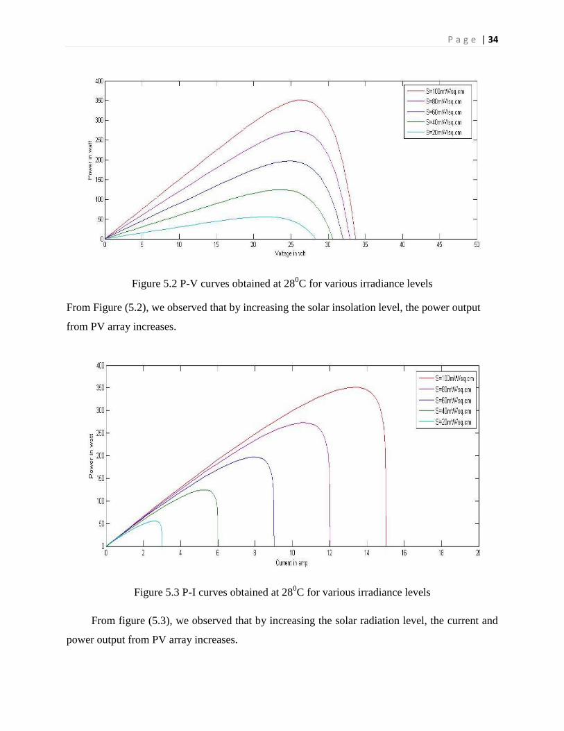
Figure 5.2 P-V curves obtained at 280C for various irradiance levels
From Figure (5.2), we observed that by increasing the solar insolation level, the power output
from PV array increases.
Figure 5.3 P-I curves obtained at 280C for various irradiance levels
From figure (5.3), we observed that by increasing the solar radiation level, the current and
power output from PV array increases.

P a g e | 35
Figure 5.4 I-V curves obtained at an irradiance of 100 mW /cm2 for various temperatures.
From figure(5.4), we observed that by increasing the temperature level at constant irradiance, the
voltage output from PV array decreases but current output increases slightly with respect to
voltage and, hence the power output from PV array decreases.
Figure 5.5 P-I curves obtained at an irradiance of 100 mW/cm2 for various temperatures.

P a g e | 36
Figure 5.6 P-V curves obtained at an irradiance of 100 mW/cm2 various temperatures.

P a g e | 37
5.3 SIMULINK MODEL
The Figure (5.7) below shows the block diagram of the complete circuit. This includes the PV
module, boost converter and control circuit. The modeling and simulation of the whole system
has been done in MATLAB-SIMULINK environment.
Figure 5.7 The complete simulation model of the PV energy conversion system.
P a g e | 38
5.4 GENERATION OF THE PWM SIGNAL
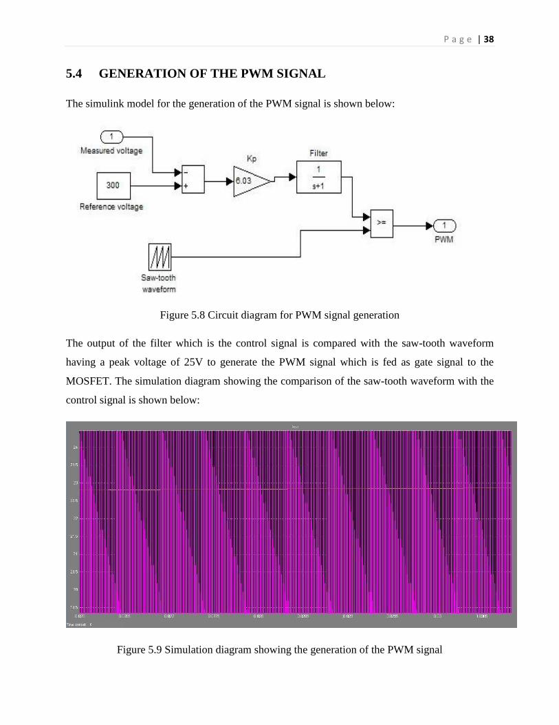
The simulink model for the generation of the PWM signal is shown below:
Figure 5.8 Circuit diagram for PWM signal generation
The output of the filter which is the control signal is compared with the saw-tooth waveform
having a peak voltage of 25V to generate the PWM signal which is fed as gate signal to the
MOSFET. The simulation diagram showing the comparison of the saw-tooth waveform with the
control signal is shown below:
Figure 5.9 Simulation diagram showing the generation of the PWM signal
P a g e | 39
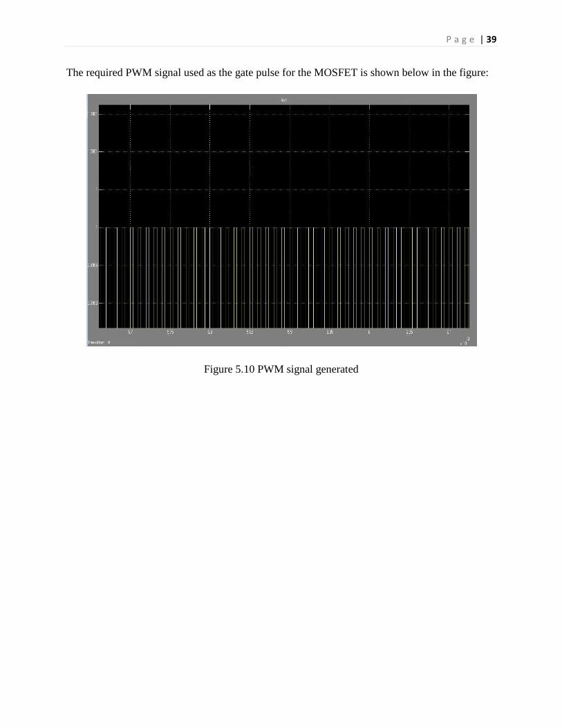
The required PWM signal used as the gate pulse for the MOSFET is shown below in the figure:
Figure 5.10 PWM signal generated
P a g e | 40
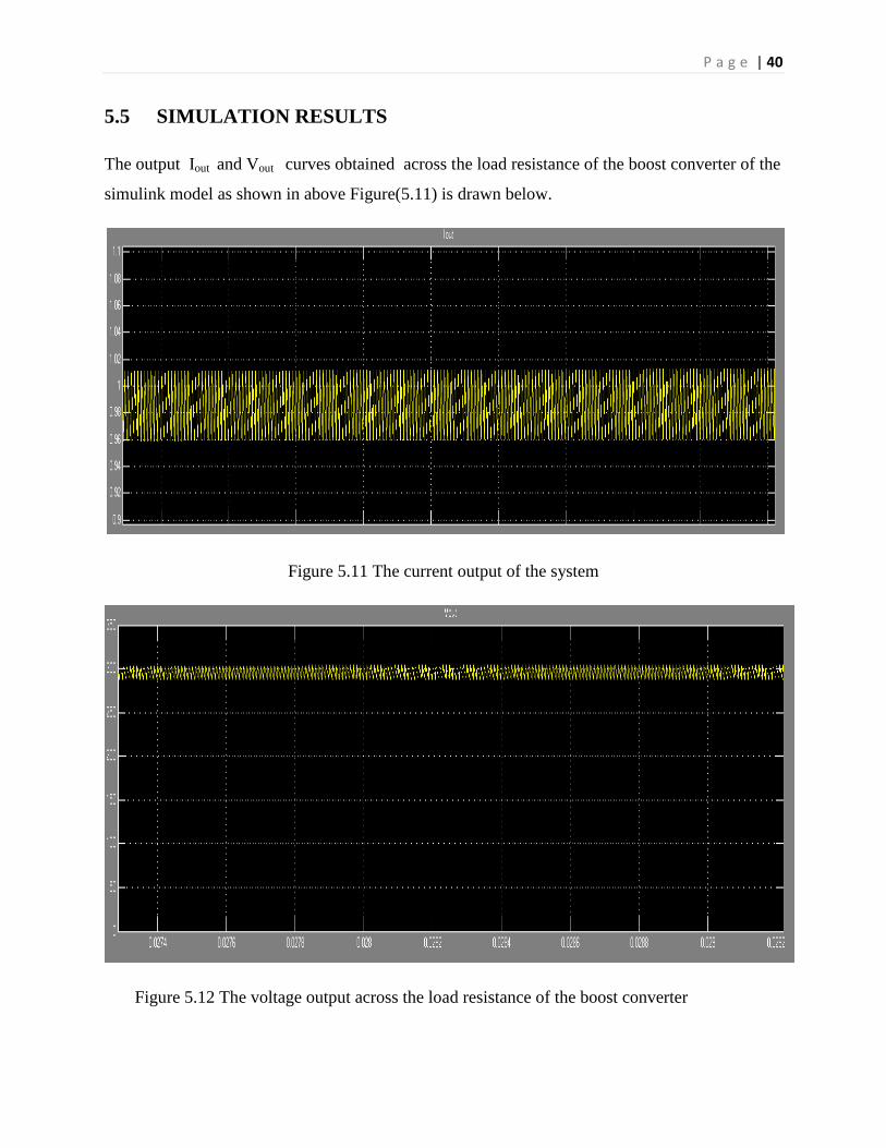
5.5 SIMULATION RESULTS
The output Iout and Vout curves obtained across the load resistance of the boost converter of the
simulink model as shown in above Figure(5.11) is drawn below.
Figure 5.11 The current output of the system
Figure 5.12 The voltage output across the load resistance of the boost converter

P a g e | 41
5.6 RESULTS CONFIRMING PROPER COUPLING OF PV ARRAY
WITH BOOST CONVERTER
The load resistance of the close loop boost converter is varied and the values of the input
voltage and current fed to the converter are noted for various levels of insolation. The values of
the current and voltage obtained are plotted in the open circuit I-V curve of the PV array. The
values obtained follow the curve closely thereby fulfilling our requirements. The tabulation and
the curves which verify our successful simulation model is given below:
Table 2: Value of input voltage and current for variation in load resistance for an irradiance level
(100 mW/m2)
INSOLATION(mW/m2)
LOAD
RESISTANCE()
INPUT
VOLTAGE(Volt)
INPUT
CURRENT(Amp)
100 300 28.92 11.42
100 285 27.2 12.86
100 450 31.62 6.898

P a g e | 42
Table 3: Value of input voltage and current for variation in load resistance for an irradiance level
(80 mW/m2)
INSOLATION(mW/m2)
LOAD
RESISTANCE()
INPUT
VOLTAGE(Volt)
INPUT
CURRENT(Amp)
80 400 28.75 8.58
80 450 29.75 7.382
80 680 31.26 4.726
Figure 5.13 Interfacing of PV array simulation result with open loop I-V characteristic

Chapter 6
CONCLUSIONS

P a g e | 44
The open circuit P-V, P-I, I-V curves we obtained from the simulation of the PV array designed
in MATLAB environment explains in detail its dependence on the irradiation levels and
temperatures. The entire energy conversion system has been designed in MATLB-SIMULINK
environment. The various values of the voltage and current obtained have been plotted in the
open circuit I-V curves of the PV array at insolation levels of 100 mW/cm2 and 80 mW/cm
2. The
voltage and current values lie on the curve showing that the coupling of the PV array with the
boost converter is proper. However the performance of the photovoltaic device depends on the
spectral distribution of the solar radiation.

REFERENCES

P a g e | 46
1. I.H Atlas, A.M Sharaf, "A photovoltaic Array Simulation Model for Matlab-
Simulink GUI Environment”, Proce. of IEEE International Conference on Clean
Electrical Power, ICCEP 2007, Capri, Italy.
2. Jesus Leyva-Ramos, Member, IEEE, and Jorge Alberto Morales-Saldana," A
design criteria for the current gain in Current Programmed Regulators", IEEE
Transactions on industrial electronics, Vol. 45, No. 4, August 1998.
3. K.H. Hussein, I. Muta, T. Hoshino, M. Osakada, "Maximum photovoltaic power
tracking: an algorithm for rapidly changing atmospheric conditions", IEE Proc.-
Gener. Trans. Distrib., Vol. 142,No. 1, January 1995.
4. Md. Rabiul Islam, Youguang Guo, Jian Guo Zhu, M.G Rabbani, "Simulation of
PV Array Characteristics and Fabrication of Microcontroller Based MPPT",
Faculty of Engineering and Information technology, University of Technology
Sydney, Australia, 6th International Conference on Electrical and Computer
Engineering ICECE 2010, 18-20 December 2010, Dhaka, Bangladesh.
5. W. Xiao, W. G. Dunford, and A. Capel, “A novel modeling method for
photovoltaic cells”, in Proc. IEEE 35th Annu. Power Electron. Spec. Conf.
(PESC), 2004, vol. 3, pp. 1950–1956.
6. IEEE Standard Definitions of Terms for Solar Cells, 1969.
7. Oliva Mah NSPRI, "Fundamentals of Photovoltaic Materials", National Solar
power institute, Inc. 12/21/98.
8. Muhammad H. Rashid, “Power Electronics Circuits, Devices and Applications”,
Third Edition.
9. Modelling and Control design for DC-DC converter, Power Management group,
AVLSI Lab, IIT-Kharagpur.
10. Nielsen, R. 2005, 'Solar Radiation', http://home.iprimus.com.au/nielsens/
11. www.earthscan.co.uk/Portals/
12. Application of non-conventional & renewable energy sources, Bureau of Energy
Efficiency.
13. http://en.wikipedia.org/wiki/Solar_power
14. http://en.wikipedia.org/wiki/Photovoltaic_system
15. http://en.wikipedia.org/wiki/Solar_panel
16. http://www.blueplanet-energy.com/images/solar/PV-cell-module-array.gif/
17. http://www.rids-nepal.org/index.php/Solar_Photo_Voltaic.html

P a g e | 47
18. http://alexgomez.com/autoxtra.htm.
19. www.solarhome.ru/img/pv/IV_curve_e.jpg.
20. http://ecee.colorado.edu/~bart/book/eband5.htm.