MODEL DG535 Digital Delay / Pulse Generator Trigger Selection 24 Trigger Circuits 24 Trigger...
54
MODEL DG535 Digital Delay / Pulse Generator 1290-D Reamwood Avenue Sunnyvale, CA 94089 U.S.A. Phone: (408) 744-9040, Fax: (408) 744-9049 Copyright © 1994, 1997, 2000 All Rights Reserved Revision 0
Transcript of MODEL DG535 Digital Delay / Pulse Generator Trigger Selection 24 Trigger Circuits 24 Trigger...
MODEL DG535 Digital Delay / Pulse Generator
1290-D Reamwood Avenue Sunnyvale, CA 94089 U.S.A.
Phone: (408) 744-9040, Fax: (408) 744-9049
Copyright © 1994, 1997, 2000, 2006, 2017 All Rights Reserved
Revision 3.0
04/2017
i
DG535 DIGITAL DELAY / PULSE GENERATOR OPERATION AND SERVICE MANUAL
Table of Contents
CONDENSED INFORMATION Safety and Preparation for Use v Quick-Start Instructions vi DG535 Specifications vii Abridged GPIB Command List viii Error Status Byte Definition ix Instrument Status Byte Definition ix Symbols you may find on SRS Products x GUIDE TO OPERATION Introduction 1 Front Panel Features 1 Power Button 1 Liquid Crystal Display 1 Menu Keys 1 Data Entry Keys 1 Trigger Status LED's 1 Delay Outputs 1 Pulse Outputs 2 Option 06 - Trigger Inhibit Input 2 Rear Panel Features 2 Power Entry Module 2 IEEE-488 Standard Port 2 10.000 MHz Reference 2 Option 02 - ±32 Volt Rear Panel Outputs 3 Front Panel Programming 3 Trigger Menu 4 Trigger Submenus 4 Trigger Tricks 4 Delay Menus 5 Output Menus 5 AB and CD Outputs 6 GPIB Menus 6 Store and Recall Menus 7 ACCURACY, DRIFT, AND JITTER Accuracy 7 Timebase Drift 8 Jitter 8 Channel to Channel Interaction 9
ii
Time Delay vs Repetition 9 GPIB PROGRAMMING Detailed Command List 9 Initialization Commands 9 Status Commands 9 Error Status Byte Definition 10 Instrument Status Byte Definition 10 Display Control Commands 11 Delay and Output Commands 13 Delays 13 Output Control 13 Trigger Commands 14 Store and Recall Commands 15 TROUBLESHOOTING LCD Contrast 16 Cold-Boot 16 Quick Test 16 Output Levels 16 Jitter 16 GPIB Problems 17 CALIBRATION Required Equipment 18 Calibration Procedure 18 Trigger Threshold Calibration 18 Optional 1 ppm Internal Timebase Calibration 18
Calibration Menus 19 Output Amplitude Calibration 19
Output Offset Calibration 20 Jitter Calibration 20 CIRCUIT DESCRIPTION Microprocessor System 21 IEEE-488 Interface 21 Keypad and LED Indicators 21 LCD Display 21 Output Ports on the Top PCB 21 Output Ports on the Bottom PCB 21 Port Address Decoding 22 Input Ports 22 Digital to Analog Converter 23 Timebase 23 Frequency Synthesizer 23 Line Trigger 23
iii
Trigger Selection 24 Trigger Circuits 24 Trigger Sequence 24 Overview of the Delay Channels 24 Jitter Compensation 25 Jitter Precharge and Sample & Hold 25 Kickpulse 26 The T0 Delay 26 Channel A's Digital Delay 26 Analog Delays 26 Reset Cycle and Status Bits 27
Output Drivers 27 Offset Control 27 Impedance Control 28 Gate Output Drivers 28 Power Supplies 28 Rear Panel Output Drivers 29 PARTS LISTS Top PC Board 31
Bottom PC Board 31 Front and Rear Panel 36
Optional Outputs PC Board 36 Miscellaneous and Chassis Assembly 37
PC LAYOUT Top PCB 38 Bottom PCB 39 Front PCB 40 Optional Outputs PCB 40 FAST TRANSITION-TIME MODULES 41 SCHEMATIC DIAGRAMS 45 Top PCB Sheet #1 Microprocessor System, GPIB and Digital I/O Sheet #2 Slow Counter/Timers Sheet #3 Trigger Status and Reset Sequence Sheet #4 Rate Generators Sheet #5 Power Supply and Dropout Detection Sheet #6 System Connectors and Polarity Control Bottom PCB Sheet #1 Trigger Circuit and Gated 80 MHz Sheet #2 10 MHz Reference and 80 MHz PLL Sheet #3 Jitter Compensation Sheet #4 ECL Counters and Resync Circuits
iv
Sheet #5 T0 Analog Delay and Output Driver Sheet #6 A Analog Delay and Output Driver Sheet #7 B Analog Delay and Output Driver Sheet #8 C Analog Delay and Output Driver Sheet #9 D Analog Delay and Output Driver Sheet #10 AB & CD Gate Output Drivers Sheet #11 Digital to Analog Converter and Multiplexer Sheet #12 Power Regulators Front PCB Optional Outputs PCB
Table of Figures
Figure - 1 DG535 Rear Panel Page - 2 Figure - 2 DG535 Front Panel Page - 3 Figure - 3 Maximum Error vs. Time Delay Page - 6 Figure - 4 Apparent (Peak To Peak) Jitter and RMS Jitter Page - 7 Figure - 5 RMS Jitter Page - 8 Figure - 6 DG535 Block Diagram Page - 30 Figure - 7 DG535 Timing Diagram Page - 31 Figure - 8 Top PC Layout Page - 39 Figure - 9 Bottom PC Layout Page - 40 Figure - 10 Front PC Layout Page - 41 Figure - 11 Optional Outputs PC Layout Page - 41 Figure - 12 Fast Transition-Time Modules Page - 42 Figure - 13 Fast 2 Volt Output Step Page - 44
v
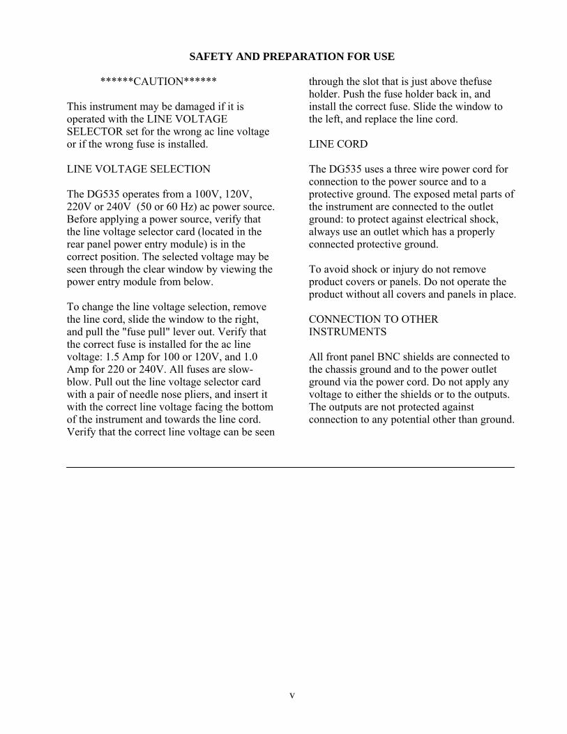
SAFETY AND PREPARATION FOR USE ******CAUTION****** This instrument may be damaged if it is operated with the LINE VOLTAGE SELECTOR set for the wrong ac line voltage or if the wrong fuse is installed. LINE VOLTAGE SELECTION The DG535 operates from a 100V, 120V, 220V or 240V (50 or 60 Hz) ac power source. Before applying a power source, verify that the line voltage selector card (located in the rear panel power entry module) is in the correct position. The selected voltage may be seen through the clear window by viewing the power entry module from below. To change the line voltage selection, remove the line cord, slide the window to the right, and pull the "fuse pull" lever out. Verify that the correct fuse is installed for the ac line voltage: 1.5 Amp for 100 or 120V, and 1.0 Amp for 220 or 240V. All fuses are slow-blow. Pull out the line voltage selector card with a pair of needle nose pliers, and insert it with the correct line voltage facing the bottom of the instrument and towards the line cord. Verify that the correct line voltage can be seen
through the slot that is just above thefuse holder. Push the fuse holder back in, and install the correct fuse. Slide the window to the left, and replace the line cord. LINE CORD The DG535 uses a three wire power cord for connection to the power source and to a protective ground. The exposed metal parts of the instrument are connected to the outlet ground: to protect against electrical shock, always use an outlet which has a properly connected protective ground. To avoid shock or injury do not remove product covers or panels. Do not operate the product without all covers and panels in place. CONNECTION TO OTHER INSTRUMENTS All front panel BNC shields are connected to the chassis ground and to the power outlet ground via the power cord. Do not apply any voltage to either the shields or to the outputs. The outputs are not protected against connection to any potential other than ground.
vi
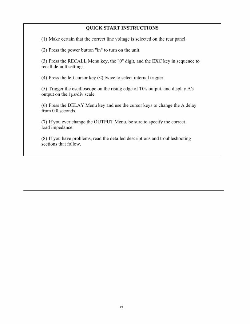
QUICK START INSTRUCTIONS
(1) Make certain that the correct line voltage is selected on the rear panel.
(2) Press the power button "in" to turn on the unit.
(3) Press the RECALL Menu key, the "0" digit, and the EXC key in sequence to recall default settings.
(4) Press the left cursor key (<) twice to select internal trigger.
(5) Trigger the oscilloscope on the rising edge of T0's output, and display A's output on the 1µs/div scale.
(6) Press the DELAY Menu key and use the cursor keys to change the A delay from 0.0 seconds.
(7) If you ever change the OUTPUT Menu, be sure to specify the correct load impedance.
(8) If you have problems, read the detailed descriptions and troubleshooting sections that follow.
vii
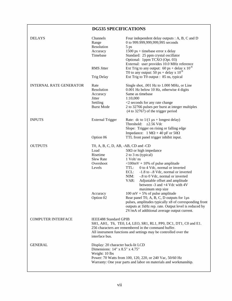
DG535 SPECIFICATIONS DELAYS Channels Four independent delay outputs : A, B, C and D Range 0 to 999.999,999,999,995 seconds Resolution 5 ps Accuracy 1500 ps + timebase error x delay Timebase Standard: 25 ppm crystal oscillator Optional: 1ppm TCXO (Opt. 03) External: user provides 10.0 MHz reference RMS Jitter Ext Trig to any output: 60 ps + delay x 10-8 T0 to any output: 50 ps + delay x 10-8 Trig Delay Ext Trig to T0 output : 85 ns, typical INTERNAL RATE GENERATOR Rate Single shot, .001 Hz to 1.000 MHz, or Line Resolution 0.001 Hz below 10 Hz, otherwise 4 digits Accuracy Same as timebase Jitter 1:10,000 Settling <2 seconds for any rate change Burst Mode 2 to 32766 pulses per burst at integer multiples (4 to 32767) of the trigger period INPUTS External Trigger Rate: dc to 1/(1 µs + longest delay) Threshold: ±2.56 Vdc Slope: Trigger on rising or falling edge Impedance: 1 MΩ + 40 pF or 50Ω Option 06 TTL front panel trigger inhibit input. OUTPUTS T0, A, B, C, D, AB, -AB, CD and -CD Load 50Ω or high impedance Risetime 2 to 3 ns (typical) Slew Rate 1 Volt/ ns Overshoot <100mV + 10% of pulse amplitude Levels TTL: 0 to 4 Vdc, normal or inverted ECL: -1.8 to -.8 Vdc, normal or inverted NIM: -.8 to 0 Vdc, normal or inverted VAR: Adjustable offset and amplitude between -3 and +4 Vdc with 4V maximum step size Accuracy 100 mV + 5% of pulse amplitude Option 02 Rear panel T0, A, B, C, D outputs for 1µs
pulses, amplitudes typically x8 of corresponding front outputs at 1kHz rep. rate. Output level is reduced by 2V/mA of additional average output current.
COMPUTER INTERFACE IEEE488 Standard GPIB SH1, AH1, T6, TE0, L4, LEO, SR1, RL1, PP0, DC1, DT1, C0 and E1. 256 characters are remembered in the command buffer. All instrument functions and settings may be controlled over the interface bus. GENERAL Display: 20 character back-lit LCD
Dimensions: 14" x 8.5" x 4.75" Weight: 10 lbs Power: 70 Watts from 100, 120, 220, or 240 Vac, 50/60 Hz Warranty: One year parts and labor on materials and workmanship.
viii
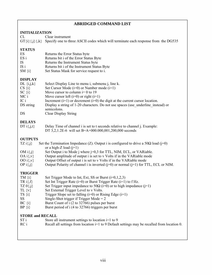
ABRIDGED COMMAND LIST INITIALIZATION CL Clear instrument GTi,j,k Specify one to three ASCII codes which will terminate each response from the DG535 STATUS ES Returns the Error Status byte ES i Returns bit i of the Error Status Byte IS Returns the Instrument Status byte IS i Returns bit i of the Instrument Status Byte SM i Set Status Mask for service request to i. DISPLAY DL i,j,k Select Display Line to menu i, submenu j, line k. CS i Set Cursor Mode (i=0) or Number mode (i=1) SC i Move cursor to column i= 0 to 19 MC i Move cursor left (i=0) or right (i=1) IC i Increment (i=1) or decrement (i=0) the digit at the current cursor location. DS string Display a string of 1-20 characters. Do not use spaces (use_underline_instead) or
semicolons. DS Clear Display String DELAYS DT i,j,t Delay Time of channel i is set to t seconds relative to channel j. Example: DT 3,2,1.2E-6 will set B=A+000.000,001,200,000 seconds OUTPUTS TZ i,j Set the Termination Impedance (Z). Output i is configured to drive a 50Ω load (j=0) or a high-Z load (j=1) OM i,j Set Output i to Mode j where j=0,3 for TTL, NIM, ECL, or VARiable. OA i,v Output amplitude of output i is set to v Volts if in the VARiable mode OO i,v Output Offset of output i is set to v Volts if in the VARiable mode OP i,j Output Polarity of channel i is inverted (j=0) or normal (j=1) for TTL, ECL or NIM. TRIGGER TM i Set Trigger Mode to Int, Ext, SS or Burst (i=0,1,2,3) TR i,f Set Int Trigger Rate (i=0) or Burst Trigger Rate (i=1) to f Hz. TZ 0,j Set Trigger input impedance to 50Ω (i=0) or to high impedance (j=1) TL v Set External Trigger Level to v Volts. TS i Trigger Slope set to falling (i=0) or Rising Edge (i=1) SS Single-Shot trigger if Trigger Mode = 2 BC i Burst Count of i (2 to 32766) pulses per burst BP i Burst period of i (4 to 32766) triggers per burst STORE and RECALL ST i Store all instrument settings to location i=1 to 9 RC i Recall all settings from location i=1 to 9 Default settings may be recalled from location 0.
ix
NOTES In all of the commands listed here, i, j and k are integer values and f, t and v may be integer, floating point or exponential notation. Optional parameters are enclosed in curly brackets. If optional parameters are omitted then the current value of those parameters will be sent back to the GPIB controller. For example, the command "TM 3" sets the Trigger Mode to mode 3 while the command "TM" will return the response "3". Also, blanks are ignored, case is ignored, multiple commands may be sent on one line if separated by semicolons. All responses are terminated by a carriage return and a line feed. The line feed is sent with an EOI.
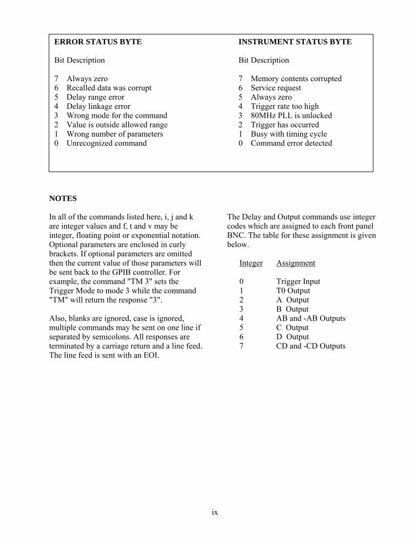
The Delay and Output commands use integer codes which are assigned to each front panel BNC. The table for these assignment is given below. Integer Assignment 0 Trigger Input 1 T0 Output 2 A Output 3 B Output 4 AB and -AB Outputs 5 C Output 6 D Output 7 CD and -CD Outputs
ERROR STATUS BYTE INSTRUMENT STATUS BYTE Bit Description Bit Description 7 Always zero 7 Memory contents corrupted 6 Recalled data was corrupt 6 Service request 5 Delay range error 5 Always zero 4 Delay linkage error 4 Trigger rate too high 3 Wrong mode for the command 3 80MHz PLL is unlocked 2 Value is outside allowed range 2 Trigger has occurred 1 Wrong number of parameters 1 Busy with timing cycle 0 Unrecognized command 0 Command error detected
x
1
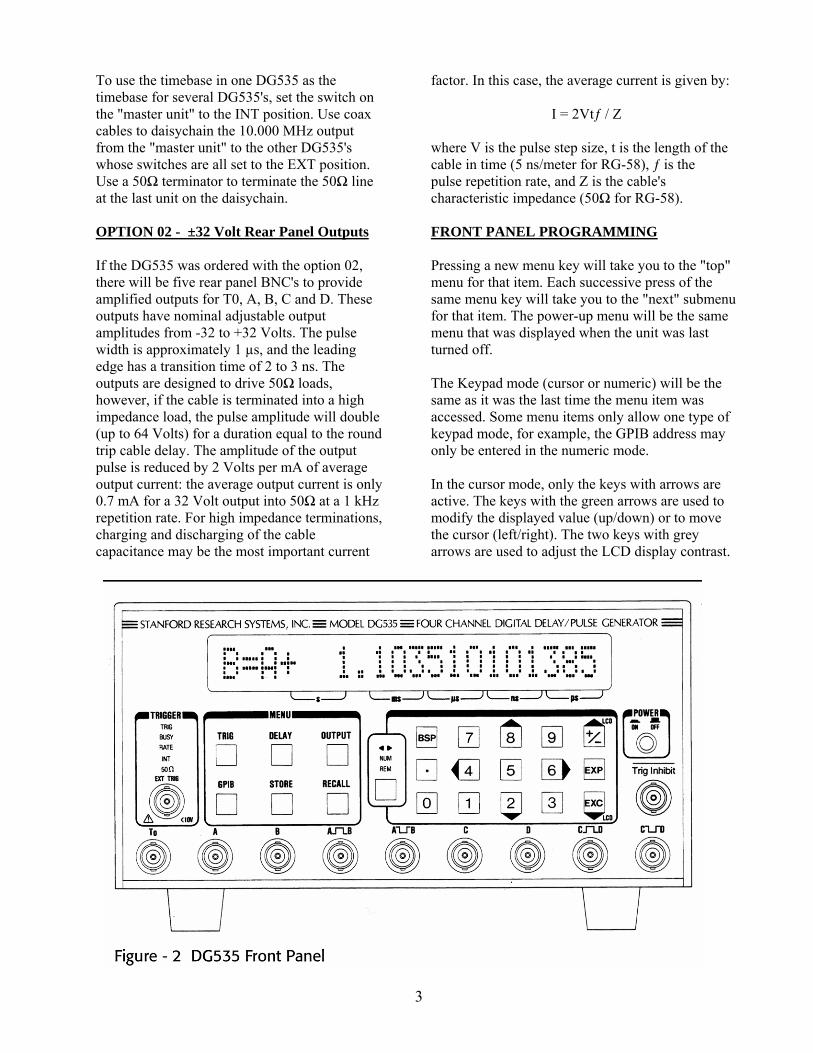
GUIDE TO OPERATION INTRODUCTION The DG535 Digital Delay and Pulse Generator can provide four precisely timed logic transitions, or two precisely controlled pulses. The four digitally controlled time intervals may be programmed from the front panel or via the GPIB. Front panel BNC's provide high slew rate outputs at TTL, NIM, ECL or continuously adjustable levels. The outputs may be set to drive either 50Ω or high impedance loads. The high accuracy (1 ppm), precision (5 ps), wide range (0 to 1000 s), and low jitter (50 ps rms) recommend the DG535 as the solution to many difficult timing problems in science and industry. FRONT PANEL OPERATION SUMMARY POWER BUTTON The unit is turned on by depressing the POWER button. All instrument settings are stored in nonvolatile RAM, and so the settings are not affected by turning the power on and off. The model, firmware version, and serial numbers for the unit will be displayed briefly when the power is first applied. LIQUID CRYSTAL DISPLAY The 20 character LCD is the user interface for all front panel programming operations. The wide viewing angle LCD is backlit by an electroluminescent panel for convenient operation in low light level conditions. When the keypad is in the cursor mode, the contrast of the LCD may be adjusted for optimum viewing by the two right most keys on the front panel. MENU KEYS Six Menu Keys select the function to be programmed. Most menu items are self-explanatory: TRIG defines the trigger source. DELAY is used to adjust the four digital delays. OUTPUT sets the output pulse levels. GPIB allows the user to see data received via
the GPIB and to set the GPIB address.
STORE and RECALL provide a convenient method to save all of the instrument settings.
Detailed descriptions of each of these menus will be given. DATA ENTRY KEYS Sixteen keys are used to enter and modify data. There are three modes of operation for this keypad: the mode is indicated by the three LED's in the center of the panel. The cursor mode (< >) allows individual digits to be modified in a fashion similar to the operation of thumbwheel switches. The numeric mode (NUM) allows the data to be entered as a numeric string. The remote mode (REM) lets the GPIB controller lock-out front panel operation. The key beneath the Mode LED's allows the user to change the keypad mode, if not locked-out by the GPIB controller. TRIGGER STATUS Five LED's are used to indicate the trigger status. The TRIG LED blinks each time the unit is triggered, the BUSY LED is on whenever a timing cycle is in progress, the RATE LED is lit if a trigger is received while BUSY. The INT LED indicates that the internal rate generator is the trigger source, and the 50Ω LED is on when the EXT TRIG input is terminated in 50Ω. The EXT TRIG BNC is the input for external triggers. DELAY OUTPUTS There are five delay output BNC's: T0, A, B, C and D. T0 marks the start of the timing interval and is most useful when an internal trigger source has been selected. The logic transitions at the outputs of A, B, C and D may be set from 0 to 1000s in 5 ps increments with respect to T0. The outputs may be programmed for TTL, NIM, ECL or adjustable output levels, and can drive 50Ω or high impedance loads. The polarity of each output may be set to provide a rising or a falling edge when the channel times out. The outputs will remain asserted until 800 ns after the longest delay. PULSE OUTPUTS There are four, pulse output BNC's: AB, -AB, CD and -CD. The AB output provides a pulse for the interval between the time set for channel A and channel B. The CD output provides a pulse for the
2
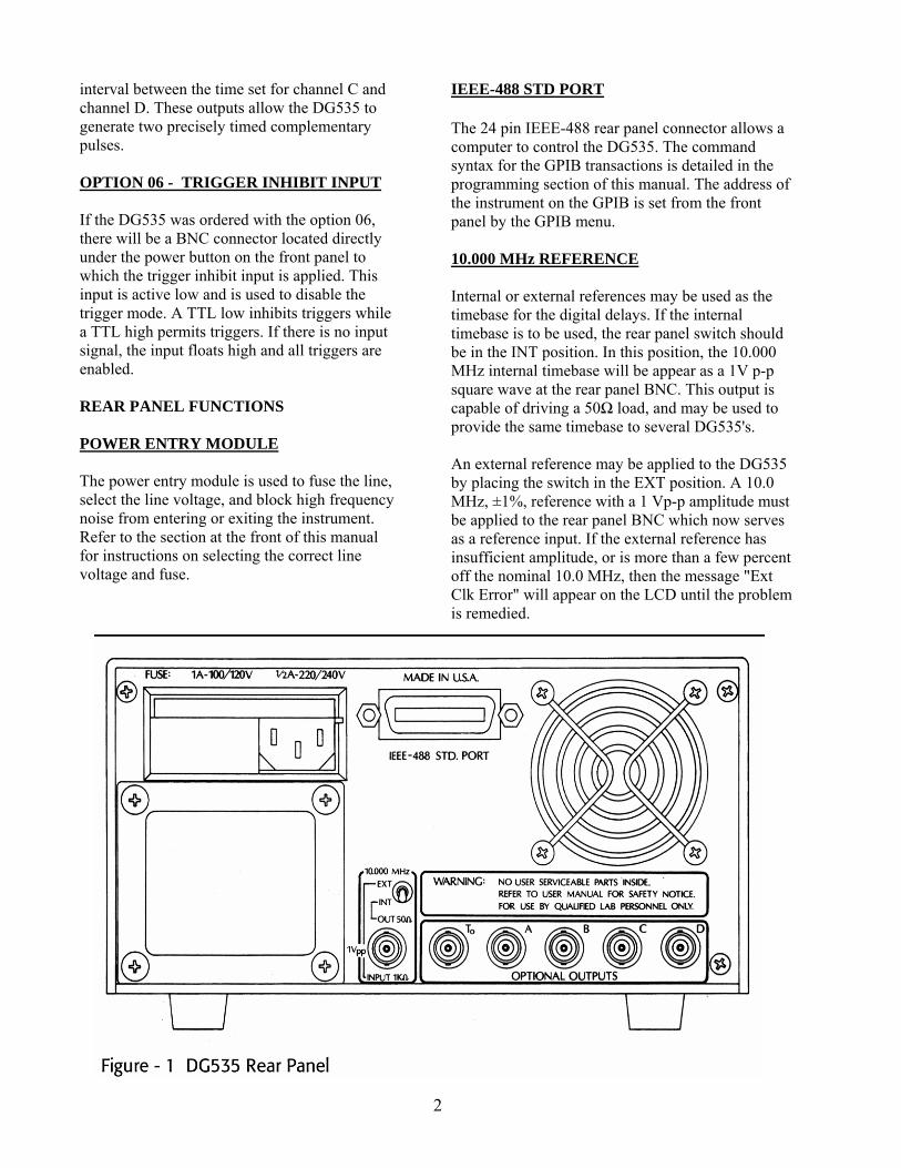
interval between the time set for channel C and channel D. These outputs allow the DG535 to generate two precisely timed complementary pulses. OPTION 06 - TRIGGER INHIBIT INPUT If the DG535 was ordered with the option 06, there will be a BNC connector located directly under the power button on the front panel to which the trigger inhibit input is applied. This input is active low and is used to disable the trigger mode. A TTL low inhibits triggers while a TTL high permits triggers. If there is no input signal, the input floats high and all triggers are enabled. REAR PANEL FUNCTIONS POWER ENTRY MODULE The power entry module is used to fuse the line, select the line voltage, and block high frequency noise from entering or exiting the instrument. Refer to the section at the front of this manual for instructions on selecting the correct line voltage and fuse.
IEEE-488 STD PORT The 24 pin IEEE-488 rear panel connector allows a computer to control the DG535. The command syntax for the GPIB transactions is detailed in the programming section of this manual. The address of the instrument on the GPIB is set from the front panel by the GPIB menu. 10.000 MHz REFERENCE Internal or external references may be used as the timebase for the digital delays. If the internal timebase is to be used, the rear panel switch should be in the INT position. In this position, the 10.000 MHz internal timebase will be appear as a 1V p-p square wave at the rear panel BNC. This output is capable of driving a 50Ω load, and may be used to provide the same timebase to several DG535's. An external reference may be applied to the DG535 by placing the switch in the EXT position. A 10.0 MHz, ±1%, reference with a 1 Vp-p amplitude must be applied to the rear panel BNC which now serves as a reference input. If the external reference has insufficient amplitude, or is more than a few percent off the nominal 10.0 MHz, then the message "Ext Clk Error" will appear on the LCD until the problem is remedied.
3
To use the timebase in one DG535 as the timebase for several DG535's, set the switch on the "master unit" to the INT position. Use coax cables to daisychain the 10.000 MHz output from the "master unit" to the other DG535's whose switches are all set to the EXT position. Use a 50Ω terminator to terminate the 50Ω line at the last unit on the daisychain. OPTION 02 - ±32 Volt Rear Panel Outputs If the DG535 was ordered with the option 02, there will be five rear panel BNC's to provide amplified outputs for T0, A, B, C and D. These outputs have nominal adjustable output amplitudes from -32 to +32 Volts. The pulse width is approximately 1 µs, and the leading edge has a transition time of 2 to 3 ns. The outputs are designed to drive 50Ω loads, however, if the cable is terminated into a high impedance load, the pulse amplitude will double (up to 64 Volts) for a duration equal to the round trip cable delay. The amplitude of the output pulse is reduced by 2 Volts per mA of average output current: the average output current is only 0.7 mA for a 32 Volt output into 50Ω at a 1 kHz repetition rate. For high impedance terminations, charging and discharging of the cable capacitance may be the most important current
factor. In this case, the average current is given by:
I = 2Vtƒ / Z where V is the pulse step size, t is the length of the cable in time (5 ns/meter for RG-58), ƒ is the pulse repetition rate, and Z is the cable's characteristic impedance (50Ω for RG-58). FRONT PANEL PROGRAMMING Pressing a new menu key will take you to the "top" menu for that item. Each successive press of the same menu key will take you to the "next" submenu for that item. The power-up menu will be the same menu that was displayed when the unit was last turned off. The Keypad mode (cursor or numeric) will be the same as it was the last time the menu item was accessed. Some menu items only allow one type of keypad mode, for example, the GPIB address may only be entered in the numeric mode. In the cursor mode, only the keys with arrows are active. The keys with the green arrows are used to modify the displayed value (up/down) or to move the cursor (left/right). The two keys with grey arrows are used to adjust the LCD display contrast.
4
In the numeric mode, the entire keypad is active. Data may be entered as a floating point number or in exponential notation. Entered data may be edited by using the BSP (backspace) key. Backspacing past the left edge of the screen will cancel the command. The entered data is actually used when the EXC (Execute) key is pressed. Selecting another menu item will have the same affect as pressing the EXC key. Error messages will appear on the LCD to indicate improper commands. For example, an attempt to decrement a delay below zero will generate the error message "Delay Range Error". The error message may be cleared from the LCD by pressing any key. TRIGGER MENU The "top" line on the trigger menu is: Int Ext SS Bur Line The cursor, underlines one of the five modes in the list to indicate Internal, External, Single-Shot, Burst, or Line trigger. The left and right cursor keys may be used to change the mode. Subsequent menus, which are different for each trigger mode, are selected by pressing the TRIG menu key again. TRIGGER SUBMENUS Mode Menu Example Int Rate =10000.000Hz Ext Threshold =+1.00V Slope(±) = + Trigger Term = HighZ SS Single-Shot (Exc) Bur Rate =10000.000Hz Pulses/Burst 10 Periods/Burst 20 Line (No submenu) The Internal trigger mode has only one submenu to set the trigger rate. The rate may be entered in the numeric mode or modified in the cursor mode. Only four digits of precision are allowed, and digits more than three places beyond the decimal point will be truncated.
The External trigger mode has three submenus to specify the threshold, slope and termination impedance of the external trigger input. Each submenu is selected by pressing the TRIG key. The Threshold may be entered as a floating point number or may be modified in the cursor mode. The Slope may be selected by using the cursor (up/down) keys, as can the Trigger termination impedance. The threshold, slope, and termination impedance shown in the example menus would be appropriate for triggering on the rising edge of a TTL Pulse. The Single-Shot trigger mode has only one submenu. If SS is selected by the cursor, pressing the TRIG menu key will display "Single Shot (EXC)." Now each press of the execute key will trigger the timing cycle. The Burst mode has three submenus to specify trigger rate, number of pulses per burst, and number of periods between the start of each burst of pulses. All of the items may be entered in the numeric mode, or modified in the cursor mode. The Rate may be entered in floating point or exponential notation, and may be specified to four digits of precision. For the entries shown in the above menu example, there would be 10 pulses per burst, each pulse separated by 100 µs, and a new burst of pulses would start every 20 periods, i.e. every 2 ms. The Line trigger mode has no submenus. The unit will be triggered on a zero crossing of the power line at the line frequency. The line trigger is also synchronized to the internal 80 MHz timebase, so that the timing jitter of the delay outputs in this trigger mode will be very low (typically 25 ps rms). TRIGGER TRICKS There are several techniques that may be used to extend the versatility of the DG535's trigger modes. The Jitter of the delay outputs will be reduced by about a factor of two (to less than 25 ps rms) if the unit is triggered synchronously with the 10 MHz time base. This is done automatically if the Line Trigger is selected. You may also want to arrange your external trigger so that it is synchronous with the 10 MHz output on the rear panel (if the internal time base is being used). It is often desirable to trigger the unit at a sub-multiple of the trigger source. Suppose you wish to trigger a laser at 10 Hz synchronously with the zero
5
crossing of the power line. In this case you would select the Line Trigger, and set channel D's delay to 95 ms. Once triggered, the DG535 will ignore other triggers until all channels have timed out, so every sixth Line trigger (at 60 Hz) will cause a new timing cycle. The RATE error LED on the front panel will be illuminated to indicate that triggers occurred while the unit was busy. Trigger rates up to 100 MHz can be used, with the unit ignoring all triggers until all channels have timed out, as in the above case. DELAY MENUS There are four delay menus to specify the delays for channels A, B, C and D. Each delay may be entered in floating point or exponential notation or may be modified in the keypad cursor mode. The maximum time delay is 999.999,999,999,995 seconds, which may be set with a resolution of 5 ps. Example Delay Menus A=T0+0.123456789125 B=A+0.001000000000 C=T0+123.456789123455 D=C+0.000000010000 Any delay channel may be "linked" to another channel. Two examples of this are shown in the above sample menus. While A is referenced to T0, channel B's delay is set to A's delay plus 0.001 seconds. Linking provides a convenient method to specify a pulse output (AB) as a pulse start time and width rather than start and stop times. Now, if channel A's delay is modified, B's delay moves with it, so that the pulse width stays at 0.001 seconds. With the above settings, the CD output will produce a very accurate 10 ns pulse despite the very long delay which is specified for channel C. To change the linkage, the cursor is positioned beneath the character just to the right of the equal sign, and the cursor up/down keys are used to select from the available links. Not all links are available, for example, in the above menus linking channel A to channel B is not allowed, as B is linked to channel A in the second menu. Delay can be scrolled by first selecting the delay menu, positioning the cursor under the digit to be incremented. Depress the #5 and either the up
or down keys simultaneously. The step rate will be approximately 4 Hz, and may vary during a scan. OUTPUT MENUS The output menus are used to specify the load impedances, pulse output amplitudes, offsets, and polarities for each of the front panel BNC's. The cursor (left/right) keys are used in the "top" line of the OUTPUT menu to select which output is to be programmed. Successive presses of the OUTPUT key will access each menu line for the selected output, finally returning to the "top" line. The menu items for the T0, A, B, C and D output are virtually identical. An example of these menus is given here for channel A's output: A:load= High Z A:TTL NIM ECL VAR A:Inverted Normal (if TTL, NIM or ECL is
selected) A:Amplitude = +1.00V (if VARiable is selected) A:Offset = 0.50V (if VARiable is selected) The first line in this submenu specifies the load impedance. The cursor (up/down) keys are used to select between High Z and 50Ω loads. This is a very important step in setting up the output: the wrong choice will cause the output to have half the expected amplitude, or to misbehave entirely. The cursor (left/right) keys are used in the second submenu to select either standard logic levels for the output, or continuously variable offsets and amplitudes. If either the TTL, NIM or ECL logic levels are selected, the next submenu is used to specify the polarity of the output pulse: the "Normal" polarity will provide a rising edge at the output at the set time: "Inverted" polarity will provide a falling edge. If VAR (variable) is selected in the second submenu, then subsequent submenus allow the pulse amplitude and offset to be set. Both numbers may be entered as floating point numbers or may be modified by the cursor keys. The minimum amplitude is 100 mV, the maximum amplitude is 4.00 VDC, and outputs outside the range of -3 to +4 VDC are not allowed.

6
AB and CD OUTPUTS The menus for the AB and CD outputs are similar to the other outputs. Example menus for the AB output are shown on the following page: AB&-AB Loads = High Z AB: TTL NIM ECL VAR AB:Amplitude = +1.00V (if VARiable is
selected) AB:Offset= +0.50V (if VARiable is selected) The cursor (up/down) keys select the load impedance for both the AB and -AB outputs. It is very important that if a 50Ω load is specified, that a 50Ω load be present on BOTH the AB and the -AB output BNC's. The cursor (left/right) keys select the logic levels for the AB and -AB outputs. If TTL, NIM or ECL is selected, then no further submenus are needed to specify the outputs: both the "Normal" and "Inverted" logic levels are available at separate front panel BNC's. If VAR is selected, then the next two submenus are used to set the amplitude and offset of the outputs.
GPIB MENUS There are three menus which are accessed by the GPIB key. They are: Data:_______________ GPIB Address: 15 Service RQST: (EXC) The first menu displays the last 15 characters of data that have been received over the GPIB. 256 characters are retained in memory and may be viewed by scrolling the display window with the cursor keys. Spaces and control codes will not be displayed, however special characters for carriage returns and line feeds will be displayed. This feature is very useful when debugging computer programs that control the DG535. The GPIB address may be set in the second menu. The keypad is automatically placed in the numeric mode for this menu item. Any address from 1 to 30 may be entered: the default address for this instrument is 15. The third menu allows the user to generate a service request by pressing the EXC button (lower right on the front panel). A service request is used to attract the attention of the GPIB controller.
7
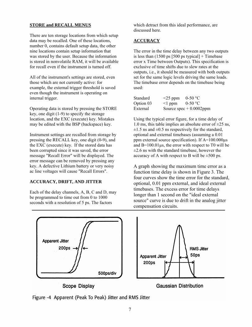
STORE and RECALL MENUS There are ten storage locations from which setup data may be recalled. One of these locations, number 0, contains default setup data, the other nine locations contain setup information that was stored by the user. Because the information is stored in nonvolatile RAM, it will be available for recall even if the instrument is turned off. All of the instrument's settings are stored, even those which are not currently active: for example, the external trigger threshold is saved even though the instrument is operating on internal trigger. Operating data is stored by pressing the STORE key, one digit (1-9) to specify the storage location, and the EXC (execute) key. Mistakes may be edited with the BSP (backspace) key. Instrument settings are recalled from storage by pressing the RECALL key, one digit (0-9), and the EXC (execute) key. If the stored data has been corrupted since it was saved, the error message "Recall Error" will be displayed. The error message can be removed by pressing any key. A defective Lithium battery or very noisy ac line voltages will cause "Recall Errors". ACCURACY, DRIFT, AND JITTER Each of the delay channels, A, B, C and D, may be programmed to time out from 0 to 1000 seconds with a resolution of 5 ps. The factors
which detract from this ideal performance, are discussed here. ACCURACY The error in the time delay between any two outputs is less than (1500 ps [500 ps typical] + Timebase error x Time between Outputs). This specification is exclusive of time shifts due to slew rates at the outputs, i.e., it should be measured with both outputs set for the same logic levels driving the same loads. The timebase error depends on the timebase being used: Standard <25 ppm 0-50 °C Option 03 <1 ppm 0-50 °C External Source spec + 0.0002ppm Using the typical error figure, for a time delay of 1.0 ms, this table implies an absolute error of ±25 ns, ±1.5 ns and ±0.5 ns respectively for the standard, optional and external timebases (assuming a 0.01 ppm external source specification). If A=100.000µs and B=100.01µs, the error with respect to T0 will be ±2.6 ns with the standard timebase, however the accuracy of A with respect to B will be ±500 ps. A graph showing the maximum time error as a function time delay is shown in Figure 3. The four curves show the time error for the standard, optional, 0.01 ppm external, and ideal external timebases. The excess error for time delays longer than 1 second on the "ideal external source" curve is due to drift in the analog jitter compensation circuits.
8
TIMEBASE DRIFT The drift of the timebase over several hours is substantially less (x10 to x100 less) than the absolute timebase error. The major factor in the timebase drift is the instrument's temperature: after the instrument has warmed up, the timebase drift is about 0.5 ppm/°C for the standard timebase, and about 0.05 ppm/°C for the optional timebase. The drift between several DG535's which are used in the same experiment may be eliminated by daisychaining the reference output from one DG535 to the reference input on the other DG535's. JITTER Various noise sources in the DG535 modulate the time delay for the outputs causing "jitter". Some of these noise sources are common to all of the channels, others are independent. The distribution of the pulses around the desired time can be approximated by a Gaussian (or "normal") distribution:
where,
p(t) = probability of pulse occurring at time t T = set time for the output (mean value)
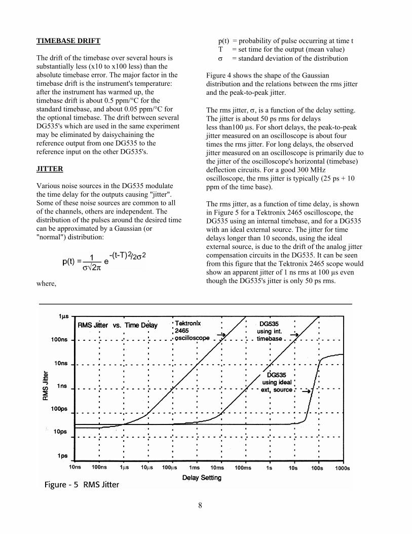
σ = standard deviation of the distribution Figure 4 shows the shape of the Gaussian distribution and the relations between the rms jitter and the peak-to-peak jitter. The rms jitter, σ, is a function of the delay setting. The jitter is about 50 ps rms for delays less than100 µs. For short delays, the peak-to-peak jitter measured on an oscilloscope is about four times the rms jitter. For long delays, the observed jitter measured on an oscilloscope is primarily due to the jitter of the oscilloscope's horizontal (timebase) deflection circuits. For a good 300 MHz oscilloscope, the rms jitter is typically (25 ps + 10 ppm of the time base). The rms jitter, as a function of time delay, is shown in Figure 5 for a Tektronix 2465 oscilloscope, the DG535 using an internal timebase, and for a DG535 with an ideal external source. The jitter for time delays longer than 10 seconds, using the ideal external source, is due to the drift of the analog jitter compensation circuits in the DG535. It can be seen from this figure that the Tektronix 2465 scope would show an apparent jitter of 1 ns rms at 100 µs even though the DG535's jitter is only 50 ps rms.
9
CHANNEL to CHANNEL INTERACTION There is a small interaction (pulling) between channels A and B and between channels C and D when these channels are set within 10 ns of each other. The pulling of one channel by the other is typically less than 100 ps. TIME DELAY vs REPETITION RATE The time delay for any channel may change by 200 ps as the pulse repetition rate is changed from single shot to the maximum rate of 1/(1 µs + longest delay). The burst mode of triggering is, effectively, a rapid change of the pulse repetition rate. GPIB PPROGRAMMING DETAILED COMMAND LIST In all of the commands listed here, i, j and k are integer values and f, t and v may be integer, floating point or exponential notation. Optional parameters are enclosed in curly brackets. In general, if optional parameters are omitted then the current value of those parameters will be sent back to the GPIB controller. For example, the command "TM 3" sets the Trigger Mode to mode 3 while the command "TM" will return the response "3". Command errors will be reported in the Error Status Byte. The controller should verify that the Error Status Byte is zero after each command is sent: a nonzero value indicates a programming problem. When an error is detected, all of the pending commands in the communication buffer are cancelled. Also, blanks are ignored, case is ignored, multiple commands may be sent on one line if separated by semicolons. All responses are terminated by a carriage return and line feed. The line feed is sent with an EOI. INITIALIZATION COMMANDS CL Clear instrument. The communication buffers are cleared and the default settings are recalled. The instrument default settings are:
Trig: Trigger mode set to Single-Shot (ie. triggers are off)
Internal: The default trigger rate is 10,000 Hz
Burst Mode: Trigger rate = 10,000Hz, 10 pulses per burst and 20 periods per burst.
External: +1VDC, positive slope, high impedance termination. Delays: All delays, A, B, C and D are linked to T0 and set to zero.
Outputs: All outputs are set to drive high impedance loads to TTL levels.
GPIB: The GPIB address is not affected, but the terminator is returned to its default value of a carriage return and a line feed with an EOI.
GTi,j,k Specify one to three ASCII codes, which will terminate each response from the DG535. The default terminator for any response from the DG535 is a carriage return and a line feed. The line feed is accompanied by an EOI. Example: to change the terminator to line feed only, the command would be "GT 10" (the ASCII code for line feed is 10 decimal). The EOI is always sent with the last character of the terminator sequence. STATUS COMMANDS ES Returns the Error Status byte. The error status byte definition is given below. Example: if a command was sent to the DG535 with too many parameters, bit 1 would be set. If the ES command is used to read the error status, and no other errors had occurred, the value "2" would be returned. All bits in the Error Status byte are latched and so will remain set until the "ES" command is executed. All bits are reset to zero after the "ES" command is executed. ES i Returns bit i of the Error Status Byte. Example: the command "ES 5" can be used to check for a delay range error. If a delay range error had occurred since the last ES or ES 5 commands had been sent, then a "1" would be returned, otherwise the value "0"
10
would be returned. This command also resets the error bit that is being checked. ERROR STATUS BYTE DEFINITION Bit Description 7 Always zero 6 Recalled data was corrupt 5 Delay range error 4 Delay linkage error 3 Wrong mode for the command 2 Value is outside allowed range 1 Wrong number of parameters 0 Unrecognized command Bit 6: This bit is set if the RC (recall stored settings) command finds that the stored values have been corrupted. A checksum is done on the settings when they are stored, and if the computed checksum on recall does not match, then the command is aborted and this error bit is set. Bit 5: This bit is set if an attempt is made to set a delay to a value below zero or above 999.999,999,999,995 seconds. Because the delay channels may be linked to each other, changing a delay to an allowed value may cause another delay to exceed the allowed range of values. Bit 4: This bit is set if an attempt is made to link delays in an illogical fashion. For example A=B+1.000 and B=A+2.000 is a condition which clearly cannot be satisfied. Bit 3: This bit is set if the instrument is not in the correct mode for the command that was sent. For example, if the instrument is set to trigger on the internal rate generator, the SS (single shot) command will be ignored and cause bit 3 to be set. Bit 2: This bit is set if the value of a parameter exceeds the allowed range for that parameter. For example, if the command "TL 20.0" is sent, the command will be ignored and bit 2 will be set (because the trigger level may only be set between ±2.56VDC). Bit 1: This bit is set if too many or too few parameters are sent with a command.
Bit 0: This bit is set if the command is completely unrecognized. IS Returns the Instrument Status byte. The definition of the instrument status byte is given below. Example: if the trigger rate to the DG535 is too high, bit 4 of the instrument status byte will be set. Sending the command "IS" will return the value "16" (if no other bits have been set). All of the bits in the instrument status byte, except for the BUSY bit, are latched, ie., if a trigger rate error is detected at any time, that bit will stay set until the "IS" command is sent. All bits, except the BUSY bit, will be reset to 0 after the "IS" command is executed. (See the IS command to test one bit of the Instrument Status byte.) IS i Returns bit i of the Instrument Status Byte. Example: the command "IS 4" will test bit 4, the "trigger rate too high" bit. The value "1" will be returned if a trigger rate error occurred since the last time the "IS" or "IS 4" command was sent. If no error had occurred, then the value "0" will be returned. INSTRUMENT STATUS BYTE DEFINITION Bit Description 7 Memory contents corrupted 6 Service request 5 Always zero 4 Trigger rate too high 3 80MHz PLL is unlocked 2 Trigger has occurred 1 Busy with timing cycle 0 Command error detected Bit 7: This bit is set if the instrument settings were corrupted since the last time power was removed. The processor computes a checksum of RAM contents, which contain the instrument settings, when a power supply dropout is detected. The checksum is again computed on power-up. If the checksums do not match, then the default settings are used (see CL command for default settings) and the message "Memory Failure" is displayed. A defective Lithium battery or very noisy ac line voltages may cause "Memory Failures" to occur. Bit 6: This bit is set if the unit is currently requesting service of the GPIB controller. A service request may be generated by a variety of conditions as specified by the service request mask. This bit
11
allows the controller to see if this instrument was the one that asserted the service request line on the GPIB. Bit 4: This bit is set if the trigger rate is too fast. The instrument requires one microsecond after the last delay has finished to reset all the delay channels. If a trigger comes during this time, then the front panel RATE LED will be turned on and bit 4 will be set. Bit 3: This bit is set if a gross error is detected in the 80MHz PLL. This can happen if the rear panel switch is set to EXT reference, and the applied 10.0MHz reference is too small or more than a few percent off the nominal 10.0MHz. If this occurs, the LCD will display the message "Ext Clk Error". Bit 2: This bit is set whenever a trigger occurs that starts a delay cycle. Triggers, which occur during a delay cycle, do not set this bit, rather they will set bit 4, the rate error bit.
Bit 1: This bit is set if the unit is currently busy with a timing cycle. Unlike all of the other status bits, it is not latched (rather it reflects the current status of the unit) and it is not reset when read by the IS command (it is reset when the unit finishes the current timing cycle.) Bit 0: This bit is set if a command error is detected. If this bit is set, the controller should read the Error Status Byte to determine the exact nature of the command error. Command errors can originate from either the GPIB or from front panel interactions. SM i Set Status Mask for service request to i. The service request status mask is used to specify which instrument Status bits will generate a GPIB service request. For example, if the command "SM 16" is sent, then a service request will be generated if the "trigger rate too high" bit is set. When a service request is generated, the corresponding bit in the Service Request Mask is turned off. This will prevent an uncontrolled stream of service requests from being generated by the DG535. To re-enable
DISPLAY CONTROL COMMAND DL i, j, k Select Display to show menu i, submenu j, line k. The menu, submenu, and line number designations are given in the table below: DISPLAY LINE SELECT TABLE i j k Display Example Comment 0 0 0 Int Ext Ss Bur Line Trigger Mode Menu 0 1 0 Rate =1234000.123Hz Internal Trigger Rate 0 2 0 Threshold = +1.23V External Trigger Menu 0 2 1 Slope(±) = + 0 2 2 Trigger Term = 50Ω 0 3 0 Single Shot (EXC) Single Shot Trigger 0 4 0 Rate =1234000.000Hz Burst Trigger Menu 0 4 1 Pulses/Burst 12345 0 4 2 Periods/Burst 12345 1 0 0 A = T+123.456789123450 Delay Menus 1 0 1 B = A- 0.123456789125 1 0 2 C = B+ 23.456789123455 1 0 3 D = T+ 0.000000000005
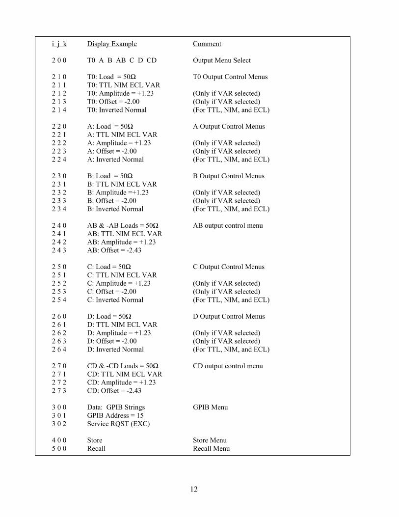
12
i j k Display Example Comment 2 0 0 T0 A B AB C D CD Output Menu Select
2 1 0 T0: Load = 50Ω T0 Output Control Menus 2 1 1 T0: TTL NIM ECL VAR 2 1 2 T0: Amplitude = +1.23 (Only if VAR selected) 2 1 3 T0: Offset = -2.00 (Only if VAR selected) 2 1 4 T0: Inverted Normal (For TTL, NIM, and ECL) 2 2 0 A: Load = 50Ω A Output Control Menus 2 2 1 A: TTL NIM ECL VAR 2 2 2 A: Amplitude = +1.23 (Only if VAR selected) 2 2 3 A: Offset = -2.00 (Only if VAR selected) 2 2 4 A: Inverted Normal (For TTL, NIM, and ECL) 2 3 0 B: Load = 50Ω B Output Control Menus 2 3 1 B: TTL NIM ECL VAR 2 3 2 B: Amplitude =+1.23 (Only if VAR selected) 2 3 3 B: Offset = -2.00 (Only if VAR selected) 2 3 4 B: Inverted Normal (For TTL, NIM, and ECL) 2 4 0 AB & -AB Loads = 50Ω AB output control menu 2 4 1 AB: TTL NIM ECL VAR 2 4 2 AB: Amplitude = +1.23 2 4 3 AB: Offset = -2.43 2 5 0 C: Load = 50Ω C Output Control Menus 2 5 1 C: TTL NIM ECL VAR 2 5 2 C: Amplitude = +1.23 (Only if VAR selected) 2 5 3 C: Offset = -2.00 (Only if VAR selected) 2 5 4 C: Inverted Normal (For TTL, NIM, and ECL) 2 6 0 D: Load = 50Ω D Output Control Menus 2 6 1 D: TTL NIM ECL VAR 2 6 2 D: Amplitude = +1.23 (Only if VAR selected) 2 6 3 D: Offset = -2.00 (Only if VAR selected) 2 6 4 D: Inverted Normal (For TTL, NIM, and ECL) 2 7 0 CD & -CD Loads = 50Ω CD output control menu 2 7 1 CD: TTL NIM ECL VAR 2 7 2 CD: Amplitude = +1.23 2 7 3 CD: Offset = -2.43 3 0 0 Data: GPIB Strings GPIB Menu 3 0 1 GPIB Address = 15 3 0 2 Service RQST (EXC) 4 0 0 Store Store Menu 5 0 0 Recall Recall Menu
13
the service request, the controller must again set the service request mask with the "SM i" command. CS i Set Cursor Mode (i=0) or Number mode (i=1). The unit must be in the cursor mode (CS 0) for the SC, MC, or IC commands to work. Note that certain menu items allow only one type of cursor mode. For example, there is no numeric mode for the menu item, which selects between TTL, NIM, ECL and VAR outputs, and there is no cursor mode in the STORE and RECALL Menus. Selecting an incorrect cursor mode will have no effect: the error will not be reported in the error status byte. SC i Move cursor to column i= 0 to 19. This command allows the controller to position the cursor under a particular digit (usually in a DELAY menu) so that the digit may be incremented or decremented by the "IC" command. A request to position the cursor in a non-allowed location (for example, under the decimal point in a time delay menu) will result in a "value outside of allowed range" error, setting bit 2 in the Error Status byte. MC i Move cursor left (i=0) or right (i=1). This command allows the cursor to be moved relative to its present position. IC i Increment (i=1) or decrement (i=0) the digit at the current cursor location. This command is used to change a displayed parameter in a manner analogous to operating a thumbwheel switch. DS string Display a string of 1 to 20 characters. This command allows the controller to display a message on the DG535's liquid crystal display. As with all data that is sent to the DG535, spaces will be stripped from the transmitted data, so the program should use the underline character to_separate_words. Also, do not use semicolons, as they are reserved characters which allow several characters to be sent on the same line. If the "DS" command is sent without a string, then the display will be cleared and the menu
item which was displayed before the "DS string" command was used will be displayed. DELAY AND OUTPUT COMMANDS The Delay and Output commands use integer codes, which are assigned to each front panel BNC. The table for these assignment is given below. Integer Assignment 0 Trigger Input 1 T0 Output 2 A Output 3 B Output 4 AB and -AB Outputs 5 C Output 6 D Output 7 CD and -CD Outputs DELAYS DT i,j,t Delay Time of channel i is set to t seconds relative to channel j. Example: DT 3,2,1.2E-6 will set B=A+0.000,001,200,000 seconds. The command DT 2,1,10.5 will set A=T0+10.500000000000 seconds. Setting delays shorter than 0 or longer than 999.999,999,999,995 seconds will set bit 2 of the Error Status Byte. A "Delay Linkage Error", bit 4 of the Error Status Byte, is caused by an attempt to totally disconnect a time reference from T0. For example the commands DT 2,3,1.5 ; DT 3,2,2.5 attempt to reference A to B and B to A so that neither is referenced to T0. This command sequence would generate a "Delay Linkage Error". An efficient method to change a delay is to position the cursor under a digit (using the SC command) and then increment/decrement the digit (using the IC command). OUTPUT CONTROL TZ i,j Set the Termination Impedance. Output i is configured to drive a 50Ω load (j=0) or a high-Z load (j=1). (If i=0, this command is used to set the impedance of the external trigger input: see the Trigger control section). Example: "TZ 4,1" will configure both the AB and -AB outputs to drive high impedance loads. The command "TZ 4" will then return the response "1", indicating that the AB and
14
-AB outputs are configured to drive high impedance loads. OM i,j Set Output i to Mode j where j=0-3 for TTL, NIM, ECL, or VARiable. This command sets the logic level of the front panel outputs. If TTL, NIM or ECL is selected, the polarity of the logic output is specified by the "OP" command. If the VARiable output mode is selected, then the output amplitude and offsets may be set with the "OA" and "OO" commands. Example: the command "OM 6,0" selects TTL levels (0 to 4VDC) for the D output. OA i,v Amplitude of output i is set to v Volts if in the VARiable mode. This command is used to set the amplitude, i.e. the size of the step, at an output BNC. The maximum step size is limited to ±4 Volts: the minimum step size is ±0.1VDC. The specified step size must not cause the output level (including the programmed offset) to exceed +4V or -3V. Example: the command sequence "OM 5,3; OO 5,0 ; OA 5,4.0" will select the VARiable mode for output C, zero its offset (see below) and set its amplitude to 4.0VDC. Note the importance of setting the offset: if the offset was set to a level greater than zero, the command "OA 5,4.0" would generate an error because the programmed offset plus amplitude would exceed the +4VDC maximum. OO i,v Output Offset of output i is set to v Volts if in the VARiable mode. This command is used to set the offset of an output when in the VARiable mode. For pulses which have a rising edge output, the offset is the voltage between the lowest output level and ground, and so a TTL signal has zero offset and +4VDC amplitude, while an ECL signal has -1.8VDC offset and a +1VDC amplitude. To invert the polarity of the pulse, i.e. for a falling edge output, a TTL output is described as a +4VDC offset an a -4VDC amplitude pulse, and an inverted ECL pulse is described by a -0.8VDC offset with a -1.0VDC amplitude. OP i,j Output Polarity of channel i is inverted (j=0) or normal (j=1) for TTL, ECL or NIM outputs. This command sets the polarity of logic pulses at the BNC outputs. In all cases, normal polarity
means that the output will provide a rising edge at the specified time. Example: the command sequence "OM 5,2; OP 5,0" will set the C output for an inverted ECL output, i.e., the output goes from -0.8VDC to -1.8VDC when the channel times out. TRIGGER COMMANDS TM i Set Trigger Mode to Int, Ext, SS or Bur (i=0,1,2,3). This command selects between Internal, External, Single-Shot, or Burst trigger modes. Other trigger commands are then used to completely specify the trigger conditions: TR will set the internal trigger rate, TL and TS set the trigger level and trigger slope for external triggers, SS is used to execute a single shot if in the SS mode, and BC and BP set the burst count and burst period for the burst mode. The TR, TL, TS, BC, and BP commands may be executed at any time, regardless of the trigger mode. Example: The command "TM 0" selects the internal rate generator as the trigger source. TR i,f Set Internal Trigger Rate (i=0) or Burst Trigger Rate (i=1) to f Hz. The frequency may be any value between 0.001 Hz and 1.000MHz. The precision is 0.001Hz below 10Hz, or 4 digits if above 10Hz. Other digits will be truncated. The internal rate generator will settle to the programmed value within 2 seconds after the command is executed: significant departures from the programmed value may be expected during the 2 second settling period. (A simple way to disable triggers during this settling time is to select the single-shot trigger mode, i.e. "TM 2".) Example: the commands "TM 0; TR 0,100.2" will select the internal trigger mode and set the trigger frequency to 100.2Hz. TL v Set External Trigger Level to v Volts. This command sets the threshold voltage for external triggers. To completely specify the external trigger, the TS (trigger slope) command must also be used. Example: "TM 1; TL 1.00; TS 1" specify the external trigger mode, with the trigger level at 1.00VDC, with a positive slope. These values would be appropriate for triggering on the rising edge of a TTL logic pulse. (Also see the TZ 0,j command which sets the input impedance for external triggers.)
15
TS i Trigger Slope set to falling (i=0) or Rising Edge (i=1). This command selects the slope condition for external triggers. It is used with the TM, TL and TZ commands to specify the conditions for an external trigger. Example: the command "TM 1; TL -1.2; TS 1; TZ 0,0" specify the external trigger mode, a trigger level of -1.2VDC, a positive trigger slope, and a trigger input impedance of 50Ω to ground. These trigger conditions would be appropriate for triggering on the rising edge of an ECL logic pulse (if it is able to drive a 50Ω load to ground.) TZ 0,j Set the input impedance of the external trigger input to 50Ω (j=0) or high impedance (j=1). Example: the command "TZ 0,1" will set the input impedance to 1 MΩ, the command "TZ 0,0" will set the input impedance to 50Ω. SS Single-Shot trigger if Trigger Mode = 2. Each time this command is issued, a new delay cycle will be initiated (if one is not already in progress) provided that the single shot trigger mode has been selected. Example: the commands "TM 2; SS; SS; SS" will place the instrument in the single-shot mode and trigger it three times. BC i Burst Count of i (2 to 32766) pulses per burst. This command is used to specify the number of pulses, which will be in each burst of pulses when in the burst mode. The Trigger Rate and Burst Period commands are also used to completely specify the burst mode of operation. Example: the command sequence "TM 3; TR 1,1000; BC 4; BP 10" selects the burst mode, sets the trigger rate to 1000Hz, and specifies 4 pulses per burst. Each burst is separated by 10 triggers, so that a new burst will start every 10ms. BP i Burst Period of i (4 to 32766) triggers per burst. This command specifies the number of triggers between the start of each burst of pulses when in the burst mode. The burst period must always be at least one larger than the Burst Count. Example: the command "TM 3; TR 1,1E5; BC 100; BP 101" sets the burst mode of operation with a trigger rate of 100KHz. There will be 100
pulses in each burst, one trigger will be skipped, and a new burst of pulses will start. STORE and RECALL COMMANDS ST i Store all instrument settings to location i=1 to 9. This command allows nine complete setups to be stored in the instrument's nonvolatile RAM. All of the instrument's settings are stored, even those that are not currently active: for example, the trigger level for external triggers will be stored even though the instrument may be operating on internal trigger. Example: the command "ST 3" will save all the instrument settings to the third storage location. RC i Recall all settings from location i=1 to 9. Default settings may be recalled from location 0. (See the CL command for the values of the default settings that are recalled from location 0.) Example: the command "RC 3" will recall all of the instrument settings which were last stored by the ST command to location 3. The display will show the menu item that was active when the ST 3 command was executed. It is possible that the memory contents of the stored settings were corrupted between the time they were stored and when they were recalled. If this happens, the message "Recall Error" will be displayed on the LCD and bit 6 of the Error Status byte will be set. Example: The command sequence "RC 3; ES 6" would recall location 3 and check bit 6 of the Error Status byte. If a "1" is returned by the "ES 6" command, then the stored values were found to be corrupted, and so the instrument setting will not be changed. Memory contents may be lost if the Lithium battery is defective or if large line transients occur.
16
TROUBLESHOOTING To start, make sure that the power entry module on the rear panel is set for ac line voltage in your area, and that the correct fuse is installed. The programmed voltage may be seen through a window when the power entry module is viewed from the bottom of the unit. Verify that the line cord is plugged all the way into the power entry module, and that the power button on the front panel is pressed "in". When the ac power is applied, you should be able to hear the fan: the unit will not function properly if the fan is not operating or if the side or bottom vent holes are blocked. Set the rear panel switch "down" to select the INT timebase. If this switch is "up", and a reference is not applied, then the error message "Ext Clk Error" will appear on the LCD. LCD CONTRAST If there are no characters on the LCD, or the contrast is very poor, adjust the contrast with the two right most keys (the ones with the gray up/down arrows). The up arrow will increase the contrast, the down arrow will decrease the contrast when the keypad is in the cursor mode. COLD BOOT If the instrument turns on, but is completely unresponsive to the keyboard, then the RAM contents may have been corrupted causing the instrument to "hang". To remedy this situation, turn the unit off, then hold down the BSP (backspace) key down and turn the unit back on again. This procedure initializes the RAM. User calibration parameters will be overwritten by the factory calibration parameters and GPIB address will be set to 15. QUICK TEST Unplug all cables from the unit and recall the "default" settings by pressing the "RECALL" menu key, the "0" key, and the "EXC" key in sequence. The trigger menu will appear on the LCD with the cursor under "Ss" for single shot. Press "TRIG" to select this mode. To trigger the unit once, press the "EXC" key. The TRIG and
BUSY LED's on the left side of the instrument will blink once each time the "EXC" key is pressed. Now press the left arrow key (the "4" key) twice to select the Internal trigger source. The default trigger rate is 10 kHz, so the TRIG and BUSY LED's will now glow steadily. Trigger an oscilloscope on the rising edge of the T0 output, and use the scope to look at the output from channel A on the 1µs per division scale. The default time delays are all zero. Press the DELAY Menu Key to show the A delay setting. Use the left/right cursor keys to position the cursor beneath the 1µs digit (seventh from the right). Use the up cursor key to increment the delay in 1µs increments. The rising edge of the A output will move 1µs later each time the "up" cursor key is pressed. The RATE error LED will come on if the delay setting exceeds 99µs, as the trigger period is 100µs (10kHz) and 1µs is required for the reset cycle. If channel A is set for a longer delay than any of the other channels, its pulse will have a constant pulse width of about 800ns. OUTPUT LEVELS If an output has only half of the programmed amplitude, then it is very likely that a high impedance load was specified in the OUTPUT Menu, but a 50Ω load is attached. If an output behaves very erratically, then it is very likely that a 50Ω load was specified, but a high impedance load is attached. The pulse outputs, AB and CD, will misbehave if a 50Ω load is specified for these outputs, but a 50Ω load is attached to only one side of the pair (i.e., to the AB output but not to the -AB output). JITTER The most common causes of excess jitter are (1) incorrect external trigger threshold setting, (2) noise or amplitude fluctuations on the trigger input, (3) insufficient or excessive trigger amplitude, (4) blocked or stalled cooling fan, or (5) triggering at too high a rate. The instrument is specified to have a jitter of 50ps + 0.01ppm of the delay (rms). The peak-to-peak jitter, as seen on an oscilloscope, is approximately four times the rms jitter, hence one would expect to see about 200ps peak-to-peak on an oscilloscope for short delays.
17
GPIB PROBLEMS The first requirement for GPIB operation is to properly attach GPIB cable and to specify the correct address for the instrument. The default GPIB address is 15, but any address between 1 and 30 may be set from the front panel. To check the GPIB address, press the GPIB menu key twice. A new GPIB address may be entered by keying in the number and pressing the EXC key. The DG535 will respond to commands only if it is addressed and the Remote Enable line (REN) is asserted. When this happens, the front panel
goes to the REMote state, which disables all of the keys except the keyboard mode key, which allows the user to leave the REMote state. The program can prevent users from using the keyboard by asserting the Local-Lockout state (LLO). Different GPIB controllers expect different "string terminators" to finish each response from an instrument. The default GPIB terminator for the DG535 is a carriage return and a linefeed with an EOI. The "GT" command may be used to change the GPIB terminator if your controller requires a different one.
18
CALIBRATION There are hundreds of bytes of calibration data in ROM which are set when the instrument is calibrated at the factory. Most of these cal bytes will never need to be adjusted: they correct for unit-to-unit variations, which will not change with aging. Other calibration bytes may need to be adjusted to re-calibrate the instrument. All of the calibration bytes are stored in ROM. Those which may need to be adjusted are also stored in nonvolatile RAM. The RAM bytes are the values that are used in the operation of the instrument. These bytes are transferred from ROM to RAM when (1) the unit is first calibrated, (2) if the RAM data is found to be corrupted, or (3) by a request to "Recall Factory Cal" in the calibration menu. Only the bytes that are stored in RAM may be modified by the end user in the calibration procedure. The procedure for the adjustment of these calibration bytes is detailed here. The cal bytes are used to minimize jitter, adjust the full-scale analog delays to 12.50ns, adjust the offsets and amplitudes of the output drivers, adjust the trigger threshold offset, and to set the optional TCXO time base to exactly 10MHz. Any part, or all, of the calibration procedure may be done. If only an adjustment of the timebase is needed, is it not necessary to do the complete calibration procedure. If your re-calibration makes things worse, you can recall the factory calibration constants to restore the RAM values to their original factory settings. REQUIRED EQUIPMENT A 300MHz scope with 500ps/div timescale such as a Tektronix 2465. A frequency counter with a timebase better than 0.1ppm such as an HP 5384A with option 004 (ovenize timebase) to calibrate the optional 1ppm TCXO. A pulse generator to provide adjustable amplitude fast risetime (less than 5ns) pulses such as an SRS DG535. Several 50Ω coax cables and ten 50Ω terminators. CALIBRATION PROCEDURE Start by setting the instrument to the default settings with a RECALL 0 EXC. This will set the
trigger mode to Single shot, the delays to zero, the output levels to TTL, normal polarity, and configure the output drivers for high impedance loads. You should recall the factory calibration values. If you are going to do only a partial calibration you may wish to write down calibration values that have been recently entered so that they may reentered without redoing the calibration. To recall the factory calibration values hold down the BSP key and press the RECALL key. The message "Rcl Fact Cal (EXC)" will appear. Now press the EXC button to recall the factory calibration parameters. Trigger Threshold Calibration The trigger threshold calibration is required only if the Ext Trigger input was damaged, and the input JFET transistor, Q114, has been replaced. This calibration adjusts the input offset for the trigger input to cancel variations in the gate-to-source voltage between JFETs. ___ Recall default instrument settings by RECALL 0 EXC. ___ Select Ext trigger and set the Trigger Input
to 50 Ω ( leave the Threshold = +1.00 VDC, Slope = + )
___ Apply a 10 KHz 0 to +1.00 VDC pulse to the Ext Trigger Input.
___ Adjust the Trig Threshold value ( the last item in the BSP-GPIB Menu ) so that the TRIG LED blinks intermittently.
Optional 1 ppm Internal Timebase Calibration This procedure should be done only if the /03 optional 1ppm TCXO oscillator is installed (refer to the rear panel serial number tag). There is no adjustment for the standard 25ppm time base. ___ Set the rear panel 10.000 MHz source switch to the INT position. ___ Attach a frequency counter to the 10.0 MHz reference output BNC. This output can
provide a 1V p-p output into a 50Ω load. ___ Simultaneously press the BSP & STORE
Menu Keys. Adjust the value to set the reference frequency to 10.000000 MHz ±1Hz. This calibrates the internal time base to 0.1ppm.
19
Output Amplitude Calibration This procedure is used to calibrate the amplitude of the front panel output drivers. You will adjust calibration values to get a -0.800 VDC pulse into a high impedance load on the T0, A, B, C, D, AB and CD outputs. ___ Recall default settings: RECALL 0 EXC ___ Use the TRIG Menu key to select Int
trigger. Press TRIG again to set the rate to 100 KHz.
___ Use the DELAY Menu key to set the delays for channels B and D to 5 µs.
___ Use the OUTPUT Menu key to set all the
outputs for High-Z loads, NIM logic levels. (between 0 and -0.8 VDC.) Do this for T0, A, B, AB, C, D and CD outputs.
For each output T0, A, B, AB, C, D and CD: ___ Connect the output to the oscilloscope
input (1 MΩ input, 200 mV/div sensitivity ). ___ Hold down the BSP key and press the GPIB
key to access the amplitude calibration factor for the corresponding channel.
___ Use the Up/Down cursor keys to adjust the amplitude of the output to -0.800 VDC.
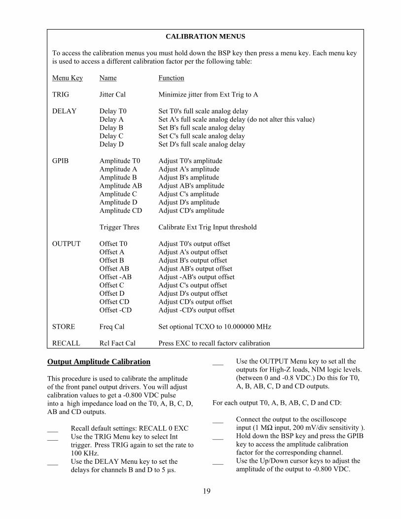
CALIBRATION MENUS
To access the calibration menus you must hold down the BSP key then press a menu key. Each menu key is used to access a different calibration factor per the following table: Menu Key Name Function TRIG Jitter Cal Minimize jitter from Ext Trig to A DELAY Delay T0 Set T0's full scale analog delay Delay A Set A's full scale analog delay (do not alter this value) Delay B Set B's full scale analog delay Delay C Set C's full scale analog delay Delay D Set D's full scale analog delay GPIB Amplitude T0 Adjust T0's amplitude Amplitude A Adjust A's amplitude Amplitude B Adjust B's amplitude Amplitude AB Adjust AB's amplitude Amplitude C Adjust C's amplitude Amplitude D Adjust D's amplitude Amplitude CD Adjust CD's amplitude Trigger Thres Calibrate Ext Trig Input threshold OUTPUT Offset T0 Adjust T0's output offset Offset A Adjust A's output offset Offset B Adjust B's output offset Offset AB Adjust AB's output offset Offset -AB Adjust -AB's output offset Offset C Adjust C's output offset Offset D Adjust D's output offset Offset CD Adjust CD's output offset Offset -CD Adjust -CD's output offset STORE Freq Cal Set optional TCXO to 10.000000 MHz RECALL Rcl Fact Cal Press EXC to recall factory calibration
20
Output Offset Calibration This procedure is used to calibrate the offset of the front panel output drivers. You will adjust calibration values to get zero offset into a high impedance load on the T0, A, B, AB, -AB, C, D, CD and the -CD outputs. ___ Recall default settings: RECALL 0 EXC ___ Use the TRIG Menu key to select Int
trigger. Press TRIG again to set the rate to 100 KHz.
___ Use the DELAY Menu key to set the delays for channel B and channel D to 5 µs.
___ Use the OUTPUT Menu key to set all the outputs for High-Z loads, NIM logic levels (between 0 and -0.8 VDC). Do this for T0, A, B, AB, C, D and CD outputs.
For each of the outputs T0, A, B, AB, -AB, C, D, CD and -CD: ___ Connect the output to the oscilloscope
input (1 MΩ input, 200 mV/div sensitivity).
___ Hold down the BSP key and press the OUTPUT key to access the Offset calibration value for the corresponding channel.
___ Use the Up/Down cursor keys to adjust the offset of the output (i.e. the top of the -0.800 V pulse) to zero.
Jitter Calibration This procedure is used to minimize the timing jitter of all the outputs with respect to an external trigger. Apply a fast risetime (<3 ns) +2 V pulse with a 10 KHz repetition rate to External Trigger input of the DG535 under test. The same pulse should also go to the CH 1 input of the oscilloscope. A good way to do this is to use the T0 output from another DG535, which has been set to drive a 50 Ω load to TTL levels. Place a tee directly on this output, with one cable to the DG535 under test, and the other cable to the oscilloscope. Both cables should be terminated into 50 Ω. With this arrangement the T0 output sees a 25 Ω load, and so the pulse amplitude will be 2 V.
The jitter from the External Trigger input to any output (T0, A, B, C or D) should be less than 50 ps rms. On a non-intensified fast oscilloscope triggered at 10 KHz, a 50 ps rms jitter will appear as about 200 ps peak-to-peak jitter. Careful attention to trigger levels and termination impedances is required to observe this small jitter. DG535 settings: ___ Recall default settings with RECALL 0
EXC ___ Select Ext trigger: +1.00 V threshold, + slope, 50 Ω Term ___ Set Delay A = 100 ns, B, C, D to 1 µs ___ Connect the A output to the oscilloscope's
CH 2 input Scope settings: ___ CH 1 and CH 2 inputs both terminated into
50 Ω ___ Trigger on CH 1 with trigger threshold set to
+1.00 V ___ 500 mV/div sensitivity on both channels. ___ Main timebase set for 50 ns/div ___ Delayed timebase set for 5 ns/div ___ Center CH 2 trace and horizontal expand
x10 to 500 ps/div ___ Change CH 2 sensitivity to 200 mV/div Jitter Cal Factor ___ Hold down the BSP key and press the TRIG
key to access the Jitter Cal factor. ___ Adjust the Jitter Cal factor to minimize the
jitter from the External trigger to the A delay output.
Delay Cal Factors For each of the channels T0, B, C and D (not A): ___ Set the delay for the selected channel to
100 ns, all other delays to 1 µs. ( Skip this step for T0 )
___ Connect the selected delay to the CH 2 input of the oscilloscope. ___ Hold down the BSP key and press the
DELAY key to access the delay factor for the corresponding delay output.
___ Adjust the delay factor to minimize the jitter between the External trigger and the delay output.

21
CIRCUIT DESCRIPTION The DG535 has three printed circuit boards. The "top" printed circuit board (Figure 8) contains the unregulated power supplies, microprocessor, GPIB interface, and the slow counters (<20MHz) that are used in each of the four time delays. The "bottom" PCB (Figure 9) contains the 80MHz PLL reference clock, ECL counters which are used in each of the four time delays, jitter compensation circuits, analog delay circuits, trigger circuits, and the fast rise time output line drivers. The "front" PCB (Figure 10) holds the key pad and status LED indicator lamps. The electroluminescent back lit LCD is mounted above the "front" PCB. A block diagram for the DG535 is depicted in Figure 6. MICROPROCESSOR SYSTEM The DG535 is controlled by a Z-80B microprocessor (U303) which is clocked by a 5MHz source which is derived from the 80MHz PLL clock on the "bottom" PCB. The unit's firmware resides in a 27128 UVEPROM (U402). This ROM also contains the calibration bytes that were determined when the unit was manufactured. The system uses 8K Bytes of RAM (U403). While operating, the supply current to the RAM comes from the +5VDC supply via D501. When the power is turned off, a Lithium battery powers the RAM via D502 (to retain the instrument settings) and RESET is asserted which disables further chip selects which are normally routed to the RAM via Q501. IEEE-488 INTERFACE The interface to the IEEE-488 is provided by U302, a TMS9914A GPIB controller. U301 and U401 are the line receiver/drivers which interface the controller IC to the IEEE-488 bus. The data bus driver is configured with open collector outputs. The controller IC handles all of the handshaking requirements to the bus, and interrupts the microprocessor if commands or data are sent to the instrument. KEY PAD and LED INDICATORS The "front" PCB, which holds the key pad and the status LED's is connected to the "top" PCB by a 20 pin ribbon cable. The octal latch, U409,
controls the eight status LED's. The eight switch lines, SWR1-SWR8, are normally held low by RN701. A key press is detected by scanning the key pad with the REM, NUM and CURS LED control lines and reading the switch input port. The diodes D709, D710, and D711 prevent simultaneous key presses from shorting out two LED control lines. LCD DISPLAY The connector to the front panel LCD, J14, ties directly to the Z-80's data bus. Besides the eight data lines on J14, there are two address lines, a chip-select, a display contrast control, +5VDC and ground. The 120 VAC required for the back lit electroluminescent display are wired directly to the 120VAC primary tap on the transformer: use caution to avoid electric shock. OUTPUT PORTS ON THE TOP PCB The Octal Buffer U408, a 74HC244, is used to buffer the Z-80's data bus to the six octal output ports and six LSI counter/timer IC's which are on the "top" PCB, and to the 40 pin connector which goes to the "bottom" PCB. This data bus buffer is only active during I/O requests by the Z-80. Octal Latch Description U202 Preset data for HC191's (A&B) U203 Preset data for HC191's (C&D) U204 Internal rate generator control U409 Front panel LED's U410 Output impedance control U411 Polarity and trigger control Each of the six LSI counter/timer IC's (uPD8253) have three independent 16 bit counter channels. Three channels are used in each of the four digital delays, and the rest are used to generate the 1KHz timer interrupt and to synthesize the clock for the internal rate generator. OUTPUT PORTS ON THE BOTTOM PCB There are two Octal Latches, U806 and U807 (on the bottom PCB), which are used to preset the ECL counters in each of the four delay channels. Another octal latch, U813, controls four 1:8 analog multiplexers to refresh 30 sample and hold circuits with the output of the 12-bit D/A converter. These
22
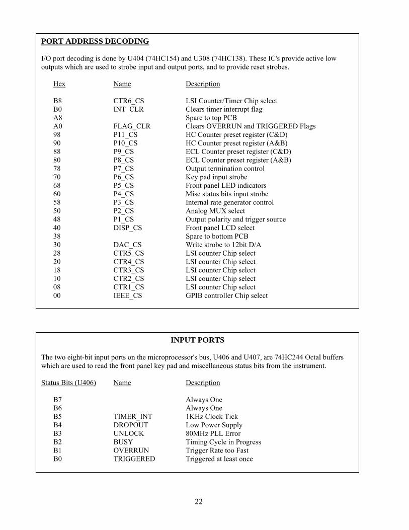
PORT ADDRESS DECODING I/O port decoding is done by U404 (74HC154) and U308 (74HC138). These IC's provide active low outputs which are used to strobe input and output ports, and to provide reset strobes. Hex Name Description B8 CTR6_CS LSI Counter/Timer Chip select B0 INT_CLR Clears timer interrupt flag A8 Spare to top PCB A0 FLAG_CLR Clears OVERRUN and TRIGGERED Flags 98 P11_CS HC Counter preset register (C&D) 90 P10_CS HC Counter preset register (A&B) 88 P9_CS ECL Counter preset register (C&D) 80 P8_CS ECL Counter preset register (A&B) 78 P7_CS Output termination control 70 P6_CS Key pad input strobe 68 P5_CS Front panel LED indicators 60 P4_CS Misc status bits input strobe 58 P3_CS Internal rate generator control 50 P2_CS Analog MUX select 48 P1_CS Output polarity and trigger source 40 DISP_CS Front panel LCD select 38 Spare to bottom PCB 30 DAC_CS Write strobe to 12bit D/A 28 CTR5_CS LSI counter Chip select 20 CTR4_CS LSI counter Chip select 18 CTR3_CS LSI counter Chip select 10 CTR2_CS LSI counter Chip select 08 CTR1_CS LSI counter Chip select 00 IEEE_CS GPIB controller Chip select
INPUT PORTS The two eight-bit input ports on the microprocessor's bus, U406 and U407, are 74HC244 Octal buffers which are used to read the front panel key pad and miscellaneous status bits from the instrument. Status Bits (U406) Name Description B7 Always One B6 Always One B5 TIMER_INT 1KHz Clock Tick B4 DROPOUT Low Power Supply B3 UNLOCK 80MHz PLL Error B2 BUSY Timing Cycle in Progress B1 OVERRUN Trigger Rate too Fast B0 TRIGGERED Triggered at least once
23
30 analog voltages are used to control amplitudes and offsets, analog time delays, external trigger threshold, reference oscillator frequency, display contrast, and to calibrate assorted current sources. Each of the 30 D/A sample and hold circuits is refreshed for 1ms every 30ms. DIGITAL TO ANALOG CONVERTER The 12-bit D/A converter is loaded by the Z-80 four bits at a time. The current output from the D/A is converted to a voltage by 1/4 of U402 with a full-scale range of 0 to -10.24VDC. The D/A voltage is offset and/or attenuated by 2/4, 3/4 and 4/4 of U402. The output of 4/4 of U402, which controls the amplitudes of all of the front panel outputs, is referenced to the -6.0VDC power supply. This is so that variations in the -6.0VDC supply will not change the amplitude current source. The output of 2/4 of U402, which controls the current sources that calibrate the analog time delay circuits, is referenced to the +15.0VDC supply. This is done so that variations in the +15.0VDC supply will not change the calibration of the analog time delays. TIMEBASE The basic time interval for all the digital delays is an 80MHz oscillator. The 80MHz is generated by a varactor-tuned VCO which is phase locked to a 10.000MHz reference. There are three sources for the 10.000MHz reference: a standard 10.000MHz reference with a 25ppm maximum error over 0 to 50°C, an optional 10.000MHz reference with a 1ppm maximum error, or a user supplied source. The optional 1ppm oscillator is powered from a doubly regulated +12VDC source (U509) and is varactor tuned by a D/A output to better than 1Hz accuracy. (See calibration procedure to set the frequency.) The internal reference is selected when the rear panel switch is in the INT position. In this position, the 10.000MHz source is shifted to ECL levels by Q502 and Q503 and passed to the ECL phase comparator U502, a MC12040 . The output of the phase comparator is filtered by the two-pole active low-pass filter (U503 and passive components). The filter output is buffered by
Q504 and used to control the frequency of the varactor-tuned LC-tank oscillator. The window comparator, U507, is used to detect gross frequency errors as might be expected if an external reference has insufficient amplitude or a frequency more than a few percent off the nominal 10.000MHz. The 80MHz output serves as the basic unit of time in all of the digital delays. The 80Mhz is divided by 8 to generate a 10MHz signal which is used to close the phase-locked-loop. The 10MHz ECL signal is shifted to TTL levels by 3/4 of U107, and buffered by Q505, to provide a nominal 1Volt square wave into 50Ω at the rear panel 10.000MHz BNC. The 10MHz TTL signal is also used as the clock to the frequency synthesizer circuits. FREQUENCY SYNTHESIZER The "bottom" PCB provides a 10 MHz frequency source to the "top" PCB, which is used as the reference for all synthesized frequencies on the "top" PCB. The 10MHz source is divided by two (1/2 U101) to generate the 5MHz clock for the Z-80. The 5MHz is in turn divided by 2 (2/2 U101) to provide a 2.5MHz clock to 3/3 of U209 (a uPD8253 Counter/Timer) which is divided by 2500 to produce a 1KHz clock to the timer interrupt flag, 1/2 U307 (a 74HC74). U112 divides the 1KHz clock to generate a 100Hz clock, which is the reference source for the internal rate synthesizer. A CMOS VCO/PLL (U110) is phase locked to an integer multiple (x1000 to x10,000 per 1/3 U210) of the 100Hz reference. The VCO output (100KHz to 1MHz) is then divided by two more LSI counter/timer channels (2/3 and 3/3 of U210)to generate any frequency between 0.001Hz and 1.000MHz. LINE TRIGGER The 8 VAC tap on the power transformer is discriminated by the comparator 1/4 of U502. This line trigger is then synchronized to the 80 MHz timebase by the flip-flop, 2/2 of U307, which is clocked by the 2.5 MHz signal, which has been divided down from the 80 MHz clock. Synchronizing the trigger to the 80 MHz timebase reduces the jitter of the delay outputs to about 25 ps rms.
24
TRIGGER SELECTION Three control bits are used to select the operating mode of the internal rate generator. These bits are set according to the selection, which is made in the TRIG Menu. If EXT trigger is selected, then the output of the rate generator is set to either 0 or 1 in order to control the polarity of the external trigger. If an INT trigger is selected, then either the VCO or the divided VCO is selected as the output to trigger the delay generator. If a BURst mode is selected, then the VCO or divided VCO is gated through U310 to produce a burst of triggers. The number of pulses in the burst is controlled by 2/3 of U209 and the interval between bursts is controlled by 1/3 of U209. The dual D-type flip-flop, U109, is used to synchronize the gate to U310 so that the falling edge of the output triggers is not affected by the propagation delay through the LSI counters. Control Bits Burst Clk_Sel Int_Trig Output 0 0 0 VCO 0 1 0 VCO/N 0 0 1 Line Trig 0 1 1 0 (Trig on Fall) 1 0 0 Burst VCO 1 1 0 Burst VCO/N 1 0 1 Line Trig 1 1 1 1 (Trig on Rise) TRIGGER CIRCUITS The digital delay generator may be triggered internally or externally. To trigger externally, the control bit EXT_TRIG is set high (Pin 19, U411 and Pin 12 on J16), and TRIG_POL is set high to trigger on rising edges or low to trigger on falling edges of the external trigger input. External triggers are discriminated by the fast Schmitt Trigger which compares the external trigger to the TRIG_THRES voltage from the D/A. The input impedance of the EXT TRIG input is 50Ω if R101 is shorted to ground by Q101 which may be turned on by a high level at TRIG_TERM. The comparator input, Q114, is protected from excessive inputs by the series impedance of R104 and R107. The input offset
voltage (due to the difference in Vgs between Q114 and Q115) is corrected by a calibration byte in the unit's ROM. The source follower outputs of the JFETs are applied to the differential pair Q102 and Q103; the outputs of this differential pair is applied to the differential pair formed by Q104 and Q105 which shifts the comparator's output to ECL levels. A 1KΩ resistor from the collector of Q104 to the source of Q114 provides about 100mV of hysteresis. The ECL output from the comparator may be inverted by the exclusive-or gate, 1/2 of U102, under the control of the TRIG_POLarity bit. If TRIG_POL=1 then the exclusive-or gate inverts the comparator's output so that a rising edge at the trigger input will trigger the unit. If INTernal trigger is selected from the trigger menu, then EXT_TRIG will be set low, forcing the output of the comparator to an ECL low level, and the unit may be triggered by a falling edge of INT_TRIG. A Single Shot trigger is done by bringing the INT_TRIG/TRIG_POL bit low once, while the EXT_TRIG bit is low. All trigger modes may be stopped by setting the TRIG_INH bit (Pin 5 of U411) to a high level. TRIGGER SEQUENCE The delay cycle is initiated when the ECL flip-flop, 1/2 U103, is clocked low. The output of this flip-flop is used to: (1) set TTL_LATCH high so that the processor can see that a timing cycle is in progress, (2) commute the current in the differential pair of Q106 and Q107 to turn off the circuit which precharges the jitter compensation voltage, (3) start the leading edge of the "Jitter Pulse" which will measure the time between the trigger and the rising edge of 80MHz clock, and (4) start a "1" shifting through the two-bit shift register formed by U105. The two-bit shift register provides an output which is synchronous with the rising edge of the 80MHz clock. This output is used to terminate the jitter pulse and to enable the five or-gates which multiplex the 80MHz clock to the ECL counters for channels T0, A, B, C, and D. OVERVIEW OF THE DELAY CHANNELS The basic time interval in the digital delay generator is the 80MHz clock, which has a period of 12.5ns. Time intervals from 0 to 1000s require that each
25
channel be able to count from 0 to 80,000,000,000 cycles of the clock. The high count rate requires using ECL, however, the large number of counts precludes using ECL exclusively. Each of the four delay channels behave like a 37 bit presettable synchronous binary ECL counter. Each channel actually consists of a 2 bit ECL counter (a 10131 dual flip-flop), a 4 bit HC counter (a 74HC191), and three 16 bit LSI counters (uPD8253's). To overcome the long propagation delays in the HC and LSI counters, there are two ECL flip-flops that re-synchronize the counter output to the 80MHz clock. Throughout the instrument there are many places where signals must be converted between ECL and HCMOS levels. To convert from ECL to HCMOS, a 10125 Quad ECL to TTL converter is used, with a resistor pull-up. To convert from HCMOS to ECL, a three-resistor network is used. Analog time delay circuits provide delays from 0 to 12.495ns so that delays may be set with a 5ps resolution. These analog delays also compensate for the jitter in the digital delay output which arises from the uncertainty in the phase of an external trigger with respect to the 80MHz internal clock. Without jitter compensation this uncertainty would give rise to a 12.5ns jitter. JITTER COMPENSATION The purpose of the jitter compensation circuit is to produce a voltage, which is proportional to the time between the trigger and a rising edge of the 80MHz clock. This voltage is used to modify the analog delays on each channel so as to eliminate this large component of output jitter. The jitter voltage is produced by integrating a constant current source on a capacitor for the time that the jitter pulse is present. The constant current source, Q113, is controlled by a D/A output from the processor. The D/A voltage, which is stored on C108, is compared to the voltage across the resistor R137. The correct D/A voltage is determined in final calibration of the instrument and is stored in the unit's ROM. A very low leakage current switch formed by Q111 and Q112 is controlled by
JITTER_PULSE. While the jitter pulse is on, all of the current is drawn from the integrating capacitor, C106. The voltage on C106 will be reduced by exactly 100mV per nanosecond of jitter pulse. The voltage on C106 is buffered by Q109, a J310 FET, level shifted by D102, a 12V Zener, to drive the base of the emitter-follower, Q110. The emitter of Q110 is the source of the jitter compensation voltage for all of the analog delay circuits. The JFET and Zener are biased by the constant current source, Q116, a JFET run at Id=Idss. Small leakage currents can cause the jitter voltage to drift. The dual op-amp, U112, prevents the jitter voltage from drifting so far as to cause a problem with the analog delay circuits. If the jitter voltage drifts up beyond the safe limit, 2/2 of U112 will lower the drain voltage to Q109 to stop the drift. (The safe upper limit threshold is reduced during the timing cycle by the size of the step at the collector of Q106. In this way, the drift limit circuit is not active while the timing cycle is not active, allowing the precharge of the integrating capacitor.) If the jitter voltage drifts down below -7.4VDC, then 1/2 of U112 will raise the voltage on the source of Q116 and so stop the downward drift. JITTER PRECHARGE AND S&H Three reference voltages are generated by the op-amp, 1/4 of U312. The input to this circuit is the +10.000VDC reference. The op-amp is configured with a gain of -1.07 to produce an output of -10.70VDC. The output is divided to produce reference levels of -7.40 and -4.00VDC. The -4.0VDC is the pre-trigger level for the jitter voltage. Before the trigger, ECL_LATCH is low and so Q107 is on, and so its collector is about 3Volts above the -15VDC supply. This will provide about 1mA to the bias input (pin 16) of the Operational Transconductance Amplifier, 1/2 U111. The OTA will source or sink current to the integrating capacitor to bring the jitter voltage to -4.0VDC. When the unit is triggered, ECL_LATCH goes high, turning off the OTA. The integrating capacitor, C106, needs to be small so that its voltage may change appreciably during the brief jitter pulse. However, small leakage currents will rapidly discharge such a small capacitor. To eliminate this problem a much larger capacitor, C104, is charged by an OTA , 2/2 of U111, to
26
provide a charge reservoir. This sample and hold OTA is active only during the first few microseconds after the trigger since the bias current to the OTA drops off as C103 discharges. KICKPULSE OTA's (Operational Transconductance Amplifiers) are used throughout the system to precharge capacitors when the delay cycle is complete. The maximum steady state bias current to these devices is only a few milliamps, so, in order to rapidly recharge these capacitors, a "kick pulse" isused to boost the current by several milliamps at the start of the reset cycle. This "kick pulse" is generated by differentiating the 800 ns GATE pulse, amplifying it with an OTA, and buffering with a Darlington pair. THE T0 DIGITAL DELAY The T0 output is similar to the A, B, C, and D output, except the delay cannot be adjusted. When a trigger is received, 4/4 of U104 gates the 80 MHz clock to U201T. The first rising edge of the 80 MHz clock sets Q-bar of 1/2 U201T, which clocks 1/2 of U103, asserting the T0-CNT to indicate the completion of the digital count for the T0 delay. The analog delay portion of the T0 delay is identical to the analog delays of the other channels. CHANNEL A's DIGITAL DELAY The digital delays are essentially identical for all of the channels; the references in this description will be to channel A. When a trigger is received, an 80MHz reference is provided by the ECL OR Gate, U106, to the two-bit ECL counter, U201A. The high bit of this counter is shifted to TTL levels by 1/4 of U203 and passed to the "top" PCB. This bit, "A/4", is used as the clock input to the 4-bit binary counter U304 (a 74HC191). The high bit of the HC counter, "A/64", is used as a clock to the uPD8253 LSI counters. The maximum clock frequency to the HC counter is 20MHz and the maximum clock frequency to the LSI counters is 1.25MHz. The quad 1:2 multiplexer, U309, passes the A inputs to the Y outputs during the count cycle.
During the 820ns reset cycle, this multiplexer sends the LOAD pulse (at the B input) to the LSI counters' clock inputs to reload the counters for the next timing cycle. The way in which the LSI counters are used depends on the number of cycles which must be counted. For very short delays, the output "A/N" may be preset high by setting the output of the last LSI counter, U206 pin 17, low. In this case, the LSI counters are not used in the delay cycle. For delays which require 1 to 32767 ticks of the HC counter in the delay, the output of the LSI counter which is connected to the or-gate is set low, allowing the last LSI counter to count the HC ticks. The last LSI counter's output goes low on the terminal count. For delays which require more than 32767 ticks of the HC counter, the LSI counter which is clocked by the inverted output of the HC counter, is programmed to divide by 32768. The next LSI counter's output will go low after 1 to 65535 ticks of the first LSI counter thus gating the HC counter's output to the last LSI counter. The last LSI counter's output goes low after 1 to 65,535 counts. The output from the HC counter (A/64) and the inverted output from the last LSI counter (A/N) are passed to the bottom PCB for synchronization to the 80MHz reference oscillator. The ECL flip-flop, 1/2 U202A, is clocked by A/64; if the D-input (A/N) is high (indicating that the LSI count is complete) then the Q-bar output of the flip-flop will go low. This eliminates the jitter of the LSI counter, as the ECL output is synchronous with the HC counter's transition. The final synchronization is done by the 2/2 of U202A. This flip flop is clocked by the ECL output of the synchronous two-bit ECL counter (20MHz toggle rate). Its output will change states synchronously with the first clock input after the Q-bar output of the 1/2 of U202A goes low. The outputs of 2/2 of U202A going low signal the end of the digital count. The channel will stop counting and the analog delay for the channel will be started. ANALOG DELAYS The analog delays for each output, T0, A, B, C and D, are essentially the same. Circuit references to channel A will be used in this description.
27
The analog delays are controlled by charging a capacitor (C309A) with a constant current source (Q304A). The constant current source, and so the delay calibration, is controlled by D/A output (A_CAL) from the processor. When the digital portion of the delay is complete, A_CNT and its complement are asserted which causes the differential pair formed by Q305A and Q306A to switch the current source away from the OTA and to the capacitor. The OTA is used to precharge the capacitor to a programmed voltage: changing the voltage will change the duration of the analog delay. The current source is calibrated to charge the capacitor at a rate of 100mV/ns, the same rate coefficient that is used in the jitter compensation circuit. The capacitor's voltage is the input to a differential comparator formed by Q307A and Q308A. The jitter voltage is applied to the other side of the comparator. When the capacitor's voltage equals the jitter compensation voltage, the analog delay times-out. In this way, the jitter of the trigger with respect to the internal 80MHz clock is canceled. The output of the differential comparator (the collector of Q308A) is applied to the ECL OR gate, 1/4 of U303. The non-inverting output of the OR gate is applied to the ECL exclusive OR gate which can invert polarity of the output pulse. The inverting output of the ECL or gate is wire-ORed with the outputs from the other channels. The reset cycle is started when this wire-ORed signal goes low, indicating that all of the delay channels have timed out. During the reset cycle, ECL_HOLD is asserted, holding the outputs of the ECL OR gate high. RESET CYCLE AND STATUS BITS An 800ns reset cycle is initiated by TTL_EOD when all of the delay channels have timed-out. TTL_EOD clocks the 2/2 of U311 high, asserting the GATE pulse. About 200ns later, C301 will be discharged by R302 and P302, and so the output of 1/6 of U312 will go high, asserting the LOAD pulse. About 250ns later, the LOAD pulse is terminated by R304 and P303 charging C303, which brings the output of the 2/2 of U312 low. The GATE pulse, and so the reset cycle, is terminated 350ns later when C302 is discharged by R303 and P301, resetting the flip-flop. U311 and U312 are powered from a separate +5.0VDC
regulator, U313, to prevent noise from modulating the reset cycle timing. The reset cycle can be initiated by the Z-80 by asserting the CPU_RELOAD signal. CPU reloads are required when the digital delays are changed, so that the counters will be preset to their new values. This signal will reset the 1/2 of U311, presetting the 2/2 of U311 and so start the reset cycle. The 1/2 of U311 is set immediately by the GATE-bar signal, enabling the circuit for the next CPU_RELOAD. Note that the HOLD pulse, which maintains the BNC outputs in their time-out state during a normal reset cycle, is disabled during a CPU initiated reset cycle. The GATE and LOAD pulses are used throughout the system to preset the ECL, HC, and LSI counters and to precharge the capacitors in the analog delays and jitter compensation circuits. Three status bits are available to allow the processor know the state of the delay cycle: BUSY is high if either TTL_LATCH is high or if a reset cycle is in progress. TRIGGERED will be high if a BUSY occurred since the last polling of this bit. OVERRUN will be set if the unit is triggered while BUSY with the current timing or reset cycle. Both TRIGGERED and OVERRUN are reset after they are polled by the Z-80 asserting the FLAG_CLR bit. OUTPUT DRIVERS The output drivers for each output, T0, A, B, C and D, are essentially the same. Circuit references to channel A will be used in this description. The outputs of the exclusive-or gate are shifted and attenuated by the resistor network N301A, and used to drive the bases of the output driver transistors Q309A and Q310A. The common emitter current source is switched between R321A and the output BNC by these transistors. The amplitude of the output pulse is set by the common emitter current source, Q316A, which is controlled by the D/A output A_AMP. OFFSET CONTROL The DC offset voltage of the outputs is controlled by the bipolar current source formed by Q302, Q303 and the op-amps 1/4 and 4/4 of U313. This current source is set by the D/A output, OFFSET_CNTL.
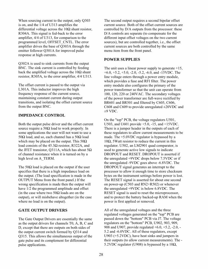
28
When sourcing current to the output, only Q303 is on, and the 1/4 of U313 amplifies the differential voltage across the 10Ω shunt resistor, R304A. This signal is fed-back to the error amplifier, 4/4 of U313, for comparison to the programmed level, OFFSET_CNTL. The error amplifier drives the base of Q303A through the emitter follower Q301A for improved pulse response at high currents. Q302A is used to sink currents from the output BNC. The sink current is controlled by feeding back the amplified voltage across the 10Ω shunt resistor, R305A, to the error amplifier, 4/4 U313. The offset current is passed to the output via L301A. This inductor improves the high frequency response of the current source, maintaining constant current during output transitions, and isolating the offset current source from the output BNC. IMPEDANCE CONTROL Both the output pulse driver and the offset current source require a 50Ω load to work properly. In some applications the user will not want to use a 50Ω load, and so, each channel has a 50Ω load which may be placed on the output. This 50Ω load consists of the 45.3Ω resistor, R322A, and the JFET transistor, Q311A, which has about 5Ω of channel resistance when it is turned on by a high level on A_TERM. The 50Ω load is placed on the output if the user specifies that there is a high impedance load on the output. (The load specification is made in the OUTPUT Menu from the front panel.) If the wrong specification is made then the output will have 1/2 the programmed amplitude and offset (in the case where two 50Ω loads are on the output), or will misbehave altogether (in the case where no load is on the output). GATE OUTPUT DRIVERS The Gate Output Drivers are essentially the same as the output drivers for channels T0, A, B, C and D, except that there are outputs on both sides of the output current switch formed by Q314 and Q315. This allows the simultaneous output of the gate pulse and its complement for differential pulse applications.
The second output requires a second bipolar offset current source. Both of the offset current sources are controlled by D/A outputs from the processor: these D/A controls are separate (to compensate for the different input offset voltages on the two current sources), but are controlled together, i.e., the offset current sources are both controlled by the same menu item from the front panel. POWER SUPPLIES The unit uses a linear power supply to generate +15, +6.0, +5.2, +5.0, -2.0, -5.2, -6.0, and -15VDC. The line voltage enters through a power entry module, which provides a fuse and RFI filter. The power entry module also configures the primary of the power transformer so that the unit can operate from 100, 120, 220 or 240VAC. The secondary voltages of the power transformer are full-wave rectified by BR601 and BR501 and filtered by C605, C606, C608 and C609 to provide unregulated ±20VDC and ±9 VDC. On the "top" PCB, the voltage regulators U501, U503, and U601 provide +5.0, -15, and +15VDC. There is a jumper header in the outputs of each of these regulators to allow current measurements to be made. The +5.0VDC regulator is bypassed by a 10Ω, 5Watt resistor to reduce the current in this regulator. U502, an LM2901 quad comparator, is used to generate active low signals to indicate DROPOUT and RESET. DROPOUT is asserted if the unregulated +9VDC drops below 7.5VDC or if the unregulated -9VDC goes above -6.8VDC. The DROPOUT signal generates an interrupt to the processor to allow it enough time to store checksum bytes on the instrument settings before power is lost. The RESET signal is asserted for about one second on power-up (C503 and RN2+R502) or whenever the unregulated +9VDC is below 6.8VDC. The RESET signal is used to reset the microprocessor, and to protect the battery backed-up RAM when the power is first applied or removed. All of the unregulated voltages and the three regulated voltages generated on the "top" PCB are passed down the "bottom" PCB via J7. The voltage regulators on the "bottom" PCB, U902, 903, 909, 908 and U907, provide regulated +6.0, +5.2, -2.0, -5.2 and -6.0VDC. All of these regulators, except U903 (+5.2VDC), have heat sinks and jumpers in their outputs (to allow current measurements). The -5.2VDC regulator (U908) is bypassed by a 10Ω,
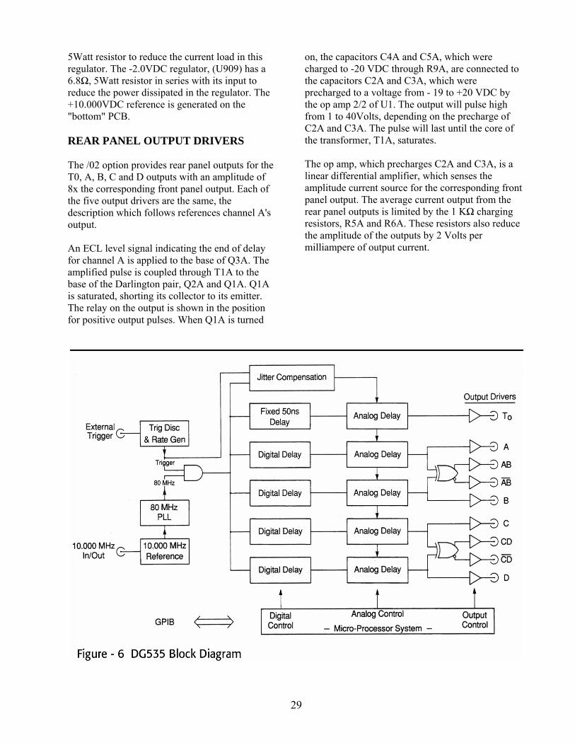
29
5Watt resistor to reduce the current load in this regulator. The -2.0VDC regulator, (U909) has a 6.8Ω, 5Watt resistor in series with its input to reduce the power dissipated in the regulator. The +10.000VDC reference is generated on the "bottom" PCB. REAR PANEL OUTPUT DRIVERS The /02 option provides rear panel outputs for the T0, A, B, C and D outputs with an amplitude of 8x the corresponding front panel output. Each of the five output drivers are the same, the description which follows references channel A's output. An ECL level signal indicating the end of delay for channel A is applied to the base of Q3A. The amplified pulse is coupled through T1A to the base of the Darlington pair, Q2A and Q1A. Q1A is saturated, shorting its collector to its emitter. The relay on the output is shown in the position for positive output pulses. When Q1A is turned
on, the capacitors C4A and C5A, which were charged to -20 VDC through R9A, are connected to the capacitors C2A and C3A, which were precharged to a voltage from - 19 to +20 VDC by the op amp 2/2 of U1. The output will pulse high from 1 to 40Volts, depending on the precharge of C2A and C3A. The pulse will last until the core of the transformer, T1A, saturates. The op amp, which precharges C2A and C3A, is a linear differential amplifier, which senses the amplitude current source for the corresponding front panel output. The average current output from the rear panel outputs is limited by the 1 KΩ charging resistors, R5A and R6A. These resistors also reduce the amplitude of the outputs by 2 Volts per milliampere of output current.
30
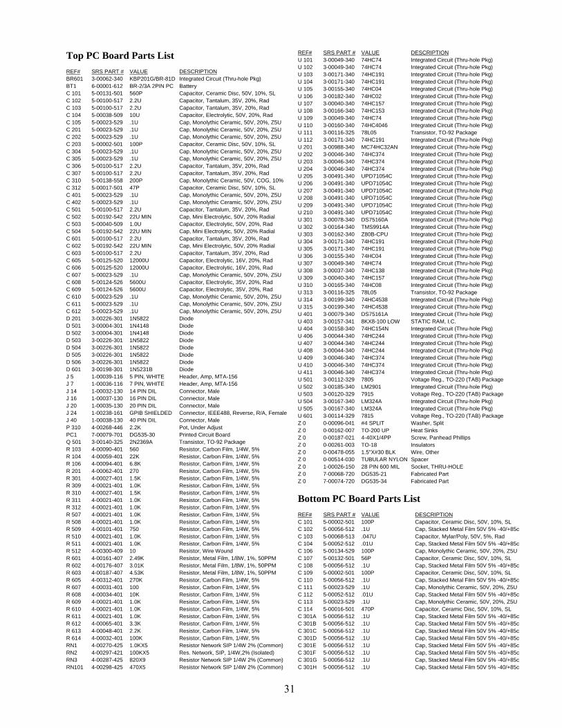
31
Top PC Board Parts List REF# SRS PART # VALUE DESCRIPTION BR601 3-00062-340 KBP201G/BR-81D Integrated Circuit (Thru-hole Pkg) BT1 6-00001-612 BR-2/3A 2PIN PC Battery C 101 5-00131-501 560P Capacitor, Ceramic Disc, 50V, 10%, SL C 102 5-00100-517 2.2U Capacitor, Tantalum, 35V, 20%, Rad C 103 5-00100-517 2.2U Capacitor, Tantalum, 35V, 20%, Rad C 104 5-00038-509 10U Capacitor, Electrolytic, 50V, 20%, Rad C 105 5-00023-529 .1U Cap, Monolythic Ceramic, 50V, 20%, Z5U C 201 5-00023-529 .1U Cap, Monolythic Ceramic, 50V, 20%, Z5U C 202 5-00023-529 .1U Cap, Monolythic Ceramic, 50V, 20%, Z5U C 203 5-00002-501 100P Capacitor, Ceramic Disc, 50V, 10%, SL C 304 5-00023-529 .1U Cap, Monolythic Ceramic, 50V, 20%, Z5U C 305 5-00023-529 .1U Cap, Monolythic Ceramic, 50V, 20%, Z5U C 306 5-00100-517 2.2U Capacitor, Tantalum, 35V, 20%, Rad C 307 5-00100-517 2.2U Capacitor, Tantalum, 35V, 20%, Rad C 310 5-00138-558 200P Cap, Monolythic Ceramic, 50V, COG, 10% C 312 5-00017-501 47P Capacitor, Ceramic Disc, 50V, 10%, SL C 401 5-00023-529 .1U Cap, Monolythic Ceramic, 50V, 20%, Z5U C 402 5-00023-529 .1U Cap, Monolythic Ceramic, 50V, 20%, Z5U C 501 5-00100-517 2.2U Capacitor, Tantalum, 35V, 20%, Rad C 502 5-00192-542 22U MIN Cap, Mini Electrolytic, 50V, 20% Radial C 503 5-00040-509 1.0U Capacitor, Electrolytic, 50V, 20%, Rad C 504 5-00192-542 22U MIN Cap, Mini Electrolytic, 50V, 20% Radial C 601 5-00100-517 2.2U Capacitor, Tantalum, 35V, 20%, Rad C 602 5-00192-542 22U MIN Cap, Mini Electrolytic, 50V, 20% Radial C 603 5-00100-517 2.2U Capacitor, Tantalum, 35V, 20%, Rad C 605 5-00125-520 12000U Capacitor, Electrolytic, 16V, 20%, Rad C 606 5-00125-520 12000U Capacitor, Electrolytic, 16V, 20%, Rad C 607 5-00023-529 .1U Cap, Monolythic Ceramic, 50V, 20%, Z5U C 608 5-00124-526 5600U Capacitor, Electrolytic, 35V, 20%, Rad C 609 5-00124-526 5600U Capacitor, Electrolytic, 35V, 20%, Rad C 610 5-00023-529 .1U Cap, Monolythic Ceramic, 50V, 20%, Z5U C 611 5-00023-529 .1U Cap, Monolythic Ceramic, 50V, 20%, Z5U C 612 5-00023-529 .1U Cap, Monolythic Ceramic, 50V, 20%, Z5U D 201 3-00226-301 1N5822 Diode D 501 3-00004-301 1N4148 Diode D 502 3-00004-301 1N4148 Diode D 503 3-00226-301 1N5822 Diode D 504 3-00226-301 1N5822 Diode D 505 3-00226-301 1N5822 Diode D 506 3-00226-301 1N5822 Diode D 601 3-00198-301 1N5231B Diode J 5 1-00039-116 5 PIN, WHITE Header, Amp, MTA-156 J 7 1-00036-116 7 PIN, WHITE Header, Amp, MTA-156 J 14 1-00032-130 14 PIN DIL Connector, Male J 16 1-00037-130 16 PIN DIL Connector, Male J 20 1-00035-130 20 PIN DIL Connector, Male J 24 1-00238-161 GPIB SHIELDED Connector, IEEE488, Reverse, R/A, FemaleJ 40 1-00038-130 40 PIN DIL Connector, Male P 310 4-00268-446 2.2K Pot, Under Adjust PC1 7-00079-701 DG535-30 Printed Circuit Board Q 501 3-00140-325 2N2369A Transistor, TO-92 Package R 103 4-00090-401 560 Resistor, Carbon Film, 1/4W, 5% R 104 4-00059-401 22K Resistor, Carbon Film, 1/4W, 5% R 106 4-00094-401 6.8K Resistor, Carbon Film, 1/4W, 5% R 201 4-00062-401 270 Resistor, Carbon Film, 1/4W, 5% R 301 4-00027-401 1.5K Resistor, Carbon Film, 1/4W, 5% R 309 4-00021-401 1.0K Resistor, Carbon Film, 1/4W, 5% R 310 4-00027-401 1.5K Resistor, Carbon Film, 1/4W, 5% R 311 4-00021-401 1.0K Resistor, Carbon Film, 1/4W, 5% R 312 4-00021-401 1.0K Resistor, Carbon Film, 1/4W, 5% R 507 4-00021-401 1.0K Resistor, Carbon Film, 1/4W, 5% R 508 4-00021-401 1.0K Resistor, Carbon Film, 1/4W, 5% R 509 4-00101-401 750 Resistor, Carbon Film, 1/4W, 5% R 510 4-00021-401 1.0K Resistor, Carbon Film, 1/4W, 5% R 511 4-00021-401 1.0K Resistor, Carbon Film, 1/4W, 5% R 512 4-00300-409 10 Resistor, Wire Wound R 601 4-00161-407 2.49K Resistor, Metal Film, 1/8W, 1%, 50PPM R 602 4-00176-407 3.01K Resistor, Metal Film, 1/8W, 1%, 50PPM R 603 4-00187-407 4.53K Resistor, Metal Film, 1/8W, 1%, 50PPM R 605 4-00312-401 270K Resistor, Carbon Film, 1/4W, 5% R 607 4-00031-401 100 Resistor, Carbon Film, 1/4W, 5% R 608 4-00034-401 10K Resistor, Carbon Film, 1/4W, 5% R 609 4-00021-401 1.0K Resistor, Carbon Film, 1/4W, 5% R 610 4-00021-401 1.0K Resistor, Carbon Film, 1/4W, 5% R 611 4-00021-401 1.0K Resistor, Carbon Film, 1/4W, 5% R 612 4-00065-401 3.3K Resistor, Carbon Film, 1/4W, 5% R 613 4-00048-401 2.2K Resistor, Carbon Film, 1/4W, 5% R 614 4-00032-401 100K Resistor, Carbon Film, 1/4W, 5% RN1 4-00270-425 1.0KX5 Resistor Network SIP 1/4W 2% (Common) RN2 4-00297-421 100KX5 Res. Network, SIP, 1/4W,2% (Isolated) RN3 4-00287-425 820X9 Resistor Network SIP 1/4W 2% (Common) RN101 4-00298-425 470X5 Resistor Network SIP 1/4W 2% (Common)
REF# SRS PART # VALUE DESCRIPTION U 101 3-00049-340 74HC74 Integrated Circuit (Thru-hole Pkg) U 102 3-00049-340 74HC74 Integrated Circuit (Thru-hole Pkg) U 103 3-00171-340 74HC191 Integrated Circuit (Thru-hole Pkg) U 104 3-00171-340 74HC191 Integrated Circuit (Thru-hole Pkg) U 105 3-00155-340 74HC04 Integrated Circuit (Thru-hole Pkg) U 106 3-00182-340 74HC02 Integrated Circuit (Thru-hole Pkg) U 107 3-00040-340 74HC157 Integrated Circuit (Thru-hole Pkg) U 108 3-00166-340 74HC153 Integrated Circuit (Thru-hole Pkg) U 109 3-00049-340 74HC74 Integrated Circuit (Thru-hole Pkg) U 110 3-00160-340 74HC4046 Integrated Circuit (Thru-hole Pkg) U 111 3-00116-325 78L05 Transistor, TO-92 Package U 112 3-00171-340 74HC191 Integrated Circuit (Thru-hole Pkg) U 201 3-00988-340 MC74HC32AN Integrated Circuit (Thru-hole Pkg) U 202 3-00046-340 74HC374 Integrated Circuit (Thru-hole Pkg) U 203 3-00046-340 74HC374 Integrated Circuit (Thru-hole Pkg) U 204 3-00046-340 74HC374 Integrated Circuit (Thru-hole Pkg) U 205 3-00491-340 UPD71054C Integrated Circuit (Thru-hole Pkg) U 206 3-00491-340 UPD71054C Integrated Circuit (Thru-hole Pkg) U 207 3-00491-340 UPD71054C Integrated Circuit (Thru-hole Pkg) U 208 3-00491-340 UPD71054C Integrated Circuit (Thru-hole Pkg) U 209 3-00491-340 UPD71054C Integrated Circuit (Thru-hole Pkg) U 210 3-00491-340 UPD71054C Integrated Circuit (Thru-hole Pkg) U 301 3-00078-340 DS75160A Integrated Circuit (Thru-hole Pkg) U 302 3-00164-340 TMS9914A Integrated Circuit (Thru-hole Pkg) U 303 3-00162-340 Z80B-CPU Integrated Circuit (Thru-hole Pkg) U 304 3-00171-340 74HC191 Integrated Circuit (Thru-hole Pkg) U 305 3-00171-340 74HC191 Integrated Circuit (Thru-hole Pkg) U 306 3-00155-340 74HC04 Integrated Circuit (Thru-hole Pkg) U 307 3-00049-340 74HC74 Integrated Circuit (Thru-hole Pkg) U 308 3-00037-340 74HC138 Integrated Circuit (Thru-hole Pkg) U 309 3-00040-340 74HC157 Integrated Circuit (Thru-hole Pkg) U 310 3-00165-340 74HC08 Integrated Circuit (Thru-hole Pkg) U 313 3-00116-325 78L05 Transistor, TO-92 Package U 314 3-00199-340 74HC4538 Integrated Circuit (Thru-hole Pkg) U 315 3-00199-340 74HC4538 Integrated Circuit (Thru-hole Pkg) U 401 3-00079-340 DS75161A Integrated Circuit (Thru-hole Pkg) U 403 3-00157-341 8KX8-100 LOW STATIC RAM, I.C. U 404 3-00158-340 74HC154N Integrated Circuit (Thru-hole Pkg) U 406 3-00044-340 74HC244 Integrated Circuit (Thru-hole Pkg) U 407 3-00044-340 74HC244 Integrated Circuit (Thru-hole Pkg) U 408 3-00044-340 74HC244 Integrated Circuit (Thru-hole Pkg) U 409 3-00046-340 74HC374 Integrated Circuit (Thru-hole Pkg) U 410 3-00046-340 74HC374 Integrated Circuit (Thru-hole Pkg) U 411 3-00046-340 74HC374 Integrated Circuit (Thru-hole Pkg) U 501 3-00112-329 7805 Voltage Reg., TO-220 (TAB) Package U 502 3-00185-340 LM2901 Integrated Circuit (Thru-hole Pkg) U 503 3-00120-329 7915 Voltage Reg., TO-220 (TAB) Package U 504 3-00167-340 LM324A Integrated Circuit (Thru-hole Pkg) U 505 3-00167-340 LM324A Integrated Circuit (Thru-hole Pkg) U 601 3-00114-329 7815 Voltage Reg., TO-220 (TAB) Package Z 0 0-00096-041 #4 SPLIT Washer, Split Z 0 0-00162-007 TO-200 UP Heat Sinks Z 0 0-00187-021 4-40X1/4PP Screw, Panhead Phillips Z 0 0-00261-003 TO-18 Insulators Z 0 0-00478-055 1.5"X#30 BLK Wire, Other Z 0 0-00514-030 TUBULAR NYLON Spacer Z 0 1-00026-150 28 PIN 600 MIL Socket, THRU-HOLE Z 0 7-00068-720 DG535-21 Fabricated Part Z 0 7-00074-720 DG535-34 Fabricated Part
Bottom PC Board Parts List REF# SRS PART # VALUE DESCRIPTION C 101 5-00002-501 100P Capacitor, Ceramic Disc, 50V, 10%, SL C 102 5-00056-512 .1U Cap, Stacked Metal Film 50V 5% -40/+85c C 103 5-00068-513 .047U Capacitor, Mylar/Poly, 50V, 5%, Rad C 104 5-00052-512 .01U Cap, Stacked Metal Film 50V 5% -40/+85c C 106 5-00134-529 100P Cap, Monolythic Ceramic, 50V, 20%, Z5U C 107 5-00132-501 56P Capacitor, Ceramic Disc, 50V, 10%, SL C 108 5-00056-512 .1U Cap, Stacked Metal Film 50V 5% -40/+85c C 109 5-00002-501 100P Capacitor, Ceramic Disc, 50V, 10%, SL C 110 5-00056-512 .1U Cap, Stacked Metal Film 50V 5% -40/+85c C 111 5-00023-529 .1U Cap, Monolythic Ceramic, 50V, 20%, Z5U C 112 5-00052-512 .01U Cap, Stacked Metal Film 50V 5% -40/+85c C 113 5-00023-529 .1U Cap, Monolythic Ceramic, 50V, 20%, Z5U C 114 5-00016-501 470P Capacitor, Ceramic Disc, 50V, 10%, SL C 301A 5-00056-512 .1U Cap, Stacked Metal Film 50V 5% -40/+85c C 301B 5-00056-512 .1U Cap, Stacked Metal Film 50V 5% -40/+85c C 301C 5-00056-512 .1U Cap, Stacked Metal Film 50V 5% -40/+85c C 301D 5-00056-512 .1U Cap, Stacked Metal Film 50V 5% -40/+85c C 301E 5-00056-512 .1U Cap, Stacked Metal Film 50V 5% -40/+85c C 301F 5-00056-512 .1U Cap, Stacked Metal Film 50V 5% -40/+85c C 301G 5-00056-512 .1U Cap, Stacked Metal Film 50V 5% -40/+85c C 301H 5-00056-512 .1U Cap, Stacked Metal Film 50V 5% -40/+85c
32
REF# SRS PART # VALUE DESCRIPTION C 301T 5-00056-512 .1U Cap, Stacked Metal Film 50V 5% -40/+85c C 302A 5-00064-513 .0047U Capacitor, Mylar/Poly, 50V, 5%, Rad C 302B 5-00064-513 .0047U Capacitor, Mylar/Poly, 50V, 5%, Rad C 302C 5-00064-513 .0047U Capacitor, Mylar/Poly, 50V, 5%, Rad C 302D 5-00064-513 .0047U Capacitor, Mylar/Poly, 50V, 5%, Rad C 302E 5-00064-513 .0047U Capacitor, Mylar/Poly, 50V, 5%, Rad C 302F 5-00064-513 .0047U Capacitor, Mylar/Poly, 50V, 5%, Rad C 302G 5-00064-513 .0047U Capacitor, Mylar/Poly, 50V, 5%, Rad C 302H 5-00064-513 .0047U Capacitor, Mylar/Poly, 50V, 5%, Rad C 302T 5-00064-513 .0047U Capacitor, Mylar/Poly, 50V, 5%, Rad C 303A 5-00023-529 .1U Cap, Monolythic Ceramic, 50V, 20%, Z5U C 303B 5-00023-529 .1U Cap, Monolythic Ceramic, 50V, 20%, Z5U C 303C 5-00023-529 .1U Cap, Monolythic Ceramic, 50V, 20%, Z5U C 303D 5-00023-529 .1U Cap, Monolythic Ceramic, 50V, 20%, Z5U C 303E 5-00023-529 .1U Cap, Monolythic Ceramic, 50V, 20%, Z5U C 303F 5-00023-529 .1U Cap, Monolythic Ceramic, 50V, 20%, Z5U C 303G 5-00023-529 .1U Cap, Monolythic Ceramic, 50V, 20%, Z5U C 303H 5-00023-529 .1U Cap, Monolythic Ceramic, 50V, 20%, Z5U C 303T 5-00023-529 .1U Cap, Monolythic Ceramic, 50V, 20%, Z5U C 304A 5-00023-529 .1U Cap, Monolythic Ceramic, 50V, 20%, Z5U C 304B 5-00023-529 .1U Cap, Monolythic Ceramic, 50V, 20%, Z5U C 304C 5-00023-529 .1U Cap, Monolythic Ceramic, 50V, 20%, Z5U C 304D 5-00023-529 .1U Cap, Monolythic Ceramic, 50V, 20%, Z5U C 304E 5-00023-529 .1U Cap, Monolythic Ceramic, 50V, 20%, Z5U C 304F 5-00023-529 .1U Cap, Monolythic Ceramic, 50V, 20%, Z5U C 304G 5-00023-529 .1U Cap, Monolythic Ceramic, 50V, 20%, Z5U C 304H 5-00023-529 .1U Cap, Monolythic Ceramic, 50V, 20%, Z5U C 304T 5-00023-529 .1U Cap, Monolythic Ceramic, 50V, 20%, Z5U C 305A 5-00056-512 .1U Cap, Stacked Metal Film 50V 5% -40/+85c C 305B 5-00056-512 .1U Cap, Stacked Metal Film 50V 5% -40/+85c C 305C 5-00056-512 .1U Cap, Stacked Metal Film 50V 5% -40/+85c C 305D 5-00056-512 .1U Cap, Stacked Metal Film 50V 5% -40/+85c C 305T 5-00056-512 .1U Cap, Stacked Metal Film 50V 5% -40/+85c C 306A 5-00002-501 100P Capacitor, Ceramic Disc, 50V, 10%, SL C 306B 5-00002-501 100P Capacitor, Ceramic Disc, 50V, 10%, SL C 306C 5-00002-501 100P Capacitor, Ceramic Disc, 50V, 10%, SL C 306D 5-00002-501 100P Capacitor, Ceramic Disc, 50V, 10%, SL C 306T 5-00002-501 100P Capacitor, Ceramic Disc, 50V, 10%, SL C 307A 5-00023-529 .1U Cap, Monolythic Ceramic, 50V, 20%, Z5U C 307B 5-00023-529 .1U Cap, Monolythic Ceramic, 50V, 20%, Z5U C 307C 5-00023-529 .1U Cap, Monolythic Ceramic, 50V, 20%, Z5U C 307D 5-00023-529 .1U Cap, Monolythic Ceramic, 50V, 20%, Z5U C 307T 5-00023-529 .1U Cap, Monolythic Ceramic, 50V, 20%, Z5U C 308A 5-00056-512 .1U Cap, Stacked Metal Film 50V 5% -40/+85c C 308B 5-00056-512 .1U Cap, Stacked Metal Film 50V 5% -40/+85c C 308C 5-00056-512 .1U Cap, Stacked Metal Film 50V 5% -40/+85c C 308D 5-00056-512 .1U Cap, Stacked Metal Film 50V 5% -40/+85c C 308T 5-00056-512 .1U Cap, Stacked Metal Film 50V 5% -40/+85c C 309A 5-00134-529 100P Cap, Monolythic Ceramic, 50V, 20%, Z5U C 309B 5-00134-529 100P Cap, Monolythic Ceramic, 50V, 20%, Z5U C 309C 5-00134-529 100P Cap, Monolythic Ceramic, 50V, 20%, Z5U C 309D 5-00134-529 100P Cap, Monolythic Ceramic, 50V, 20%, Z5U C 309T 5-00134-529 100P Cap, Monolythic Ceramic, 50V, 20%, Z5U C 310A 5-00002-501 100P Capacitor, Ceramic Disc, 50V, 10%, SL C 310B 5-00002-501 100P Capacitor, Ceramic Disc, 50V, 10%, SL C 310C 5-00002-501 100P Capacitor, Ceramic Disc, 50V, 10%, SL C 310D 5-00002-501 100P Capacitor, Ceramic Disc, 50V, 10%, SL C 310T 5-00002-501 100P Capacitor, Ceramic Disc, 50V, 10%, SL C 311A 5-00017-501 47P Capacitor, Ceramic Disc, 50V, 10%, SL C 311B 5-00017-501 47P Capacitor, Ceramic Disc, 50V, 10%, SL C 311C 5-00017-501 47P Capacitor, Ceramic Disc, 50V, 10%, SL C 311D 5-00017-501 47P Capacitor, Ceramic Disc, 50V, 10%, SL C 311J 5-00008-501 22P Capacitor, Ceramic Disc, 50V, 10%, SL C 311K 5-00008-501 22P Capacitor, Ceramic Disc, 50V, 10%, SL C 311T 5-00017-501 47P Capacitor, Ceramic Disc, 50V, 10%, SL C 312A 5-00008-501 22P Capacitor, Ceramic Disc, 50V, 10%, SL C 312B 5-00008-501 22P Capacitor, Ceramic Disc, 50V, 10%, SL C 312C 5-00008-501 22P Capacitor, Ceramic Disc, 50V, 10%, SL C 312D 5-00008-501 22P Capacitor, Ceramic Disc, 50V, 10%, SL C 312J 5-00008-501 22P Capacitor, Ceramic Disc, 50V, 10%, SL C 312K 5-00008-501 22P Capacitor, Ceramic Disc, 50V, 10%, SL C 312T 5-00008-501 22P Capacitor, Ceramic Disc, 50V, 10%, SL C 315A 5-00023-529 .1U Cap, Monolythic Ceramic, 50V, 20%, Z5U C 315B 5-00023-529 .1U Cap, Monolythic Ceramic, 50V, 20%, Z5U C 315C 5-00023-529 .1U Cap, Monolythic Ceramic, 50V, 20%, Z5U C 315D 5-00023-529 .1U Cap, Monolythic Ceramic, 50V, 20%, Z5U C 315T 5-00023-529 .1U Cap, Monolythic Ceramic, 50V, 20%, Z5U C 316A 5-00056-512 .1U Cap, Stacked Metal Film 50V 5% -40/+85c C 316B 5-00056-512 .1U Cap, Stacked Metal Film 50V 5% -40/+85c C 316C 5-00056-512 .1U Cap, Stacked Metal Film 50V 5% -40/+85c C 316D 5-00056-512 .1U Cap, Stacked Metal Film 50V 5% -40/+85c C 316J 5-00056-512 .1U Cap, Stacked Metal Film 50V 5% -40/+85c C 316K 5-00056-512 .1U Cap, Stacked Metal Film 50V 5% -40/+85c C 316T 5-00056-512 .1U Cap, Stacked Metal Film 50V 5% -40/+85c C 317A 5-00002-501 100P Capacitor, Ceramic Disc, 50V, 10%, SL
REF# SRS PART # VALUE DESCRIPTION C 317B 5-00002-501 100P Capacitor, Ceramic Disc, 50V, 10%, SL C 317C 5-00002-501 100P Capacitor, Ceramic Disc, 50V, 10%, SL C 317D 5-00002-501 100P Capacitor, Ceramic Disc, 50V, 10%, SL C 317J 5-00002-501 100P Capacitor, Ceramic Disc, 50V, 10%, SL C 317K 5-00002-501 100P Capacitor, Ceramic Disc, 50V, 10%, SL C 317T 5-00002-501 100P Capacitor, Ceramic Disc, 50V, 10%, SL C 318A 5-00023-529 .1U Cap, Monolythic Ceramic, 50V, 20%, Z5U C 318B 5-00023-529 .1U Cap, Monolythic Ceramic, 50V, 20%, Z5U C 318C 5-00023-529 .1U Cap, Monolythic Ceramic, 50V, 20%, Z5U C 318D 5-00023-529 .1U Cap, Monolythic Ceramic, 50V, 20%, Z5U C 318J 5-00023-529 .1U Cap, Monolythic Ceramic, 50V, 20%, Z5U C 318K 5-00023-529 .1U Cap, Monolythic Ceramic, 50V, 20%, Z5U C 318T 5-00023-529 .1U Cap, Monolythic Ceramic, 50V, 20%, Z5U C 401 5-00008-501 22P Capacitor, Ceramic Disc, 50V, 10%, SL C 402 5-00023-529 .1U Cap, Monolythic Ceramic, 50V, 20%, Z5U C 403 5-00023-529 .1U Cap, Monolythic Ceramic, 50V, 20%, Z5U C 504 5-00049-566 .001U Cap, Polyester Film 50V 5% -40/+85c Rad C 505 5-00049-566 .001U Cap, Polyester Film 50V 5% -40/+85c Rad C 506 5-00049-566 .001U Cap, Polyester Film 50V 5% -40/+85c Rad C 507 5-00056-512 .1U Cap, Stacked Metal Film 50V 5% -40/+85c C 508 5-00056-512 .1U Cap, Stacked Metal Film 50V 5% -40/+85c C 509 5-00049-566 .001U Cap, Polyester Film 50V 5% -40/+85c Rad C 510 5-00056-512 .1U Cap, Stacked Metal Film 50V 5% -40/+85c C 511 5-00023-529 .1U Cap, Monolythic Ceramic, 50V, 20%, Z5U C 512 5-00123-531 8-35P Capacitor, Variable, Under Adj., 5mm C 514 5-00056-512 .1U Cap, Stacked Metal Film 50V 5% -40/+85c C 901 5-00102-517 4.7U Capacitor, Tantalum, 35V, 20%, Rad C 902 5-00102-517 4.7U Capacitor, Tantalum, 35V, 20%, Rad C 903 5-00102-517 4.7U Capacitor, Tantalum, 35V, 20%, Rad C 904 5-00102-517 4.7U Capacitor, Tantalum, 35V, 20%, Rad C 905 5-00102-517 4.7U Capacitor, Tantalum, 35V, 20%, Rad C 906 5-00102-517 4.7U Capacitor, Tantalum, 35V, 20%, Rad C 907 5-00102-517 4.7U Capacitor, Tantalum, 35V, 20%, Rad C 909 5-00192-542 22U MIN Cap, Mini Electrolytic, 50V, 20% Radial C 910 5-00098-517 10U Capacitor, Tantalum, 35V, 20%, Rad C 911 5-00192-542 22U MIN Cap, Mini Electrolytic, 50V, 20% Radial C 912 5-00100-517 2.2U Capacitor, Tantalum, 35V, 20%, Rad C 919 5-00192-542 22U MIN Cap, Mini Electrolytic, 50V, 20% Radial C 920 5-00100-517 2.2U Capacitor, Tantalum, 35V, 20%, Rad C 921 5-00192-542 22U MIN Cap, Mini Electrolytic, 50V, 20% Radial C 922 5-00100-517 2.2U Capacitor, Tantalum, 35V, 20%, Rad C 923 5-00192-542 22U MIN Cap, Mini Electrolytic, 50V, 20% Radial C 924 5-00100-517 2.2U Capacitor, Tantalum, 35V, 20%, Rad C 926 5-00038-509 10U Capacitor, Electrolytic, 50V, 20%, Rad C 927 5-00038-509 10U Capacitor, Electrolytic, 50V, 20%, Rad C 928 5-00038-509 10U Capacitor, Electrolytic, 50V, 20%, Rad C 929 5-00038-509 10U Capacitor, Electrolytic, 50V, 20%, Rad C 940 5-00023-529 .1U Cap, Monolythic Ceramic, 50V, 20%, Z5U C 941 5-00023-529 .1U Cap, Monolythic Ceramic, 50V, 20%, Z5U C 942 5-00023-529 .1U Cap, Monolythic Ceramic, 50V, 20%, Z5U C 944 5-00023-529 .1U Cap, Monolythic Ceramic, 50V, 20%, Z5U C 945 5-00023-529 .1U Cap, Monolythic Ceramic, 50V, 20%, Z5U C 951 5-00023-529 .1U Cap, Monolythic Ceramic, 50V, 20%, Z5U C 952 5-00023-529 .1U Cap, Monolythic Ceramic, 50V, 20%, Z5U C 954 5-00023-529 .1U Cap, Monolythic Ceramic, 50V, 20%, Z5U C 955 5-00023-529 .1U Cap, Monolythic Ceramic, 50V, 20%, Z5U C 956 5-00023-529 .1U Cap, Monolythic Ceramic, 50V, 20%, Z5U C 957 5-00023-529 .1U Cap, Monolythic Ceramic, 50V, 20%, Z5U C 958 5-00023-529 .1U Cap, Monolythic Ceramic, 50V, 20%, Z5U C 960 5-00023-529 .1U Cap, Monolythic Ceramic, 50V, 20%, Z5U C 961 5-00023-529 .1U Cap, Monolythic Ceramic, 50V, 20%, Z5U C 962 5-00023-529 .1U Cap, Monolythic Ceramic, 50V, 20%, Z5U C 963 5-00023-529 .1U Cap, Monolythic Ceramic, 50V, 20%, Z5U C 964 5-00023-529 .1U Cap, Monolythic Ceramic, 50V, 20%, Z5U C 965 5-00023-529 .1U Cap, Monolythic Ceramic, 50V, 20%, Z5U C 966 5-00023-529 .1U Cap, Monolythic Ceramic, 50V, 20%, Z5U C 967 5-00023-529 .1U Cap, Monolythic Ceramic, 50V, 20%, Z5U C 968 5-00023-529 .1U Cap, Monolythic Ceramic, 50V, 20%, Z5U C 969 5-00023-529 .1U Cap, Monolythic Ceramic, 50V, 20%, Z5U C 970 5-00023-529 .1U Cap, Monolythic Ceramic, 50V, 20%, Z5U C 971 5-00023-529 .1U Cap, Monolythic Ceramic, 50V, 20%, Z5U C 972 5-00023-529 .1U Cap, Monolythic Ceramic, 50V, 20%, Z5U C 973 5-00023-529 .1U Cap, Monolythic Ceramic, 50V, 20%, Z5U C 974 5-00023-529 .1U Cap, Monolythic Ceramic, 50V, 20%, Z5U C 975 5-00023-529 .1U Cap, Monolythic Ceramic, 50V, 20%, Z5U C 976 5-00023-529 .1U Cap, Monolythic Ceramic, 50V, 20%, Z5U C 977 5-00023-529 .1U Cap, Monolythic Ceramic, 50V, 20%, Z5U C 978 5-00023-529 .1U Cap, Monolythic Ceramic, 50V, 20%, Z5U C 979 5-00023-529 .1U Cap, Monolythic Ceramic, 50V, 20%, Z5U C 980 5-00023-529 .1U Cap, Monolythic Ceramic, 50V, 20%, Z5U C 981 5-00023-529 .1U Cap, Monolythic Ceramic, 50V, 20%, Z5U C 982 5-00023-529 .1U Cap, Monolythic Ceramic, 50V, 20%, Z5U C 984 5-00023-529 .1U Cap, Monolythic Ceramic, 50V, 20%, Z5U CN504 5-00141-503 .22U Capacitor, Ceramic Disc, 50V, 20%, Z5U CR509 5-00003-501 10P Capacitor, Ceramic Disc, 50V, 10%, SL
33
REF# SRS PART # VALUE DESCRIPTION D 102 3-00134-301 1N759A Diode D 104 3-00004-301 1N4148 Diode D 301A 3-00004-301 1N4148 Diode D 301B 3-00004-301 1N4148 Diode D 301C 3-00004-301 1N4148 Diode D 301D 3-00004-301 1N4148 Diode D 301T 3-00004-301 1N4148 Diode D 501 3-00004-301 1N4148 Diode D 502 3-00135-301 1N5445A Diode J 7 1-00036-116 7 PIN, WHITE Header, Amp, MTA-156 J 16 1-00037-130 16 PIN DIL Connector, Male J 40 1-00038-130 40 PIN DIL Connector, Male L 301A 6-00006-602 33U Inductor, Radial L 301B 6-00006-602 33U Inductor, Radial L 301C 6-00006-602 33U Inductor, Radial L 301D 6-00006-602 33U Inductor, Radial L 301T 6-00006-602 33U Inductor, Radial L 302J 6-00006-602 33U Inductor, Radial L 302K 6-00006-602 33U Inductor, Radial L 303J 6-00006-602 33U Inductor, Radial L 303K 6-00006-602 33U Inductor, Radial L 501 6-00012-602 .11UH Inductor, Radial N 101 4-00255-421 100X3 Res. Network, SIP, 1/4W,2% (Isolated) N 102 4-00283-421 47X4 Res. Network, SIP, 1/4W,2% (Isolated) N 103 4-00284-421 1.0KX4 Res. Network, SIP, 1/4W,2% (Isolated) N 105 4-00258-421 100KX4 Res. Network, SIP, 1/4W,2% (Isolated) N 107 4-00262-425 100X7 Resistor Network SIP 1/4W 2% (Common) N 108 4-00262-425 100X7 Resistor Network SIP 1/4W 2% (Common) N 109 4-00252-425 100X5 Resistor Network SIP 1/4W 2% (Common) N 201A 4-00262-425 100X7 Resistor Network SIP 1/4W 2% (Common) N 201B 4-00262-425 100X7 Resistor Network SIP 1/4W 2% (Common) N 201C 4-00262-425 100X7 Resistor Network SIP 1/4W 2% (Common) N 201D 4-00262-425 100X7 Resistor Network SIP 1/4W 2% (Common) N 202A 4-00318-425 820X5 Resistor Network SIP 1/4W 2% (Common) N 202B 4-00318-425 820X5 Resistor Network SIP 1/4W 2% (Common) N 202C 4-00318-425 820X5 Resistor Network SIP 1/4W 2% (Common) N 202D 4-00318-425 820X5 Resistor Network SIP 1/4W 2% (Common) N 203A 4-00298-425 470X5 Resistor Network SIP 1/4W 2% (Common) N 203B 4-00298-425 470X5 Resistor Network SIP 1/4W 2% (Common) N 203C 4-00298-425 470X5 Resistor Network SIP 1/4W 2% (Common) N 203D 4-00298-425 470X5 Resistor Network SIP 1/4W 2% (Common) N 204A 4-00319-420 470X7 Resistor Network, DIP, 1/4W,2%,8 Ind N 204B 4-00319-420 470X7 Resistor Network, DIP, 1/4W,2%,8 Ind N 204C 4-00319-420 470X7 Resistor Network, DIP, 1/4W,2%,8 Ind N 204D 4-00319-420 470X7 Resistor Network, DIP, 1/4W,2%,8 Ind N 206 4-00252-425 100X5 Resistor Network SIP 1/4W 2% (Common) N 301A 4-00248-421 150X4 Res. Network, SIP, 1/4W,2% (Isolated) N 301B 4-00248-421 150X4 Res. Network, SIP, 1/4W,2% (Isolated) N 301C 4-00248-421 150X4 Res. Network, SIP, 1/4W,2% (Isolated) N 301D 4-00248-421 150X4 Res. Network, SIP, 1/4W,2% (Isolated) N 301J 4-00248-421 150X4 Res. Network, SIP, 1/4W,2% (Isolated) N 301K 4-00248-421 150X4 Res. Network, SIP, 1/4W,2% (Isolated) N 301T 4-00248-421 150X4 Res. Network, SIP, 1/4W,2% (Isolated) N 302 4-00252-425 100X5 Resistor Network SIP 1/4W 2% (Common) N 303 4-00252-425 100X5 Resistor Network SIP 1/4W 2% (Common) N 304 4-00285-421 470X3 Res. Network, SIP, 1/4W,2% (Isolated) N 305 4-00293-421 470X4 Res. Network, SIP, 1/4W,2% (Isolated) N 306 4-00313-425 390X7 Resistor Network SIP 1/4W 2% (Common) N 307 4-00266-421 4.7KX3 Res. Network, SIP, 1/4W,2% (Isolated) N 308 4-00245-421 4.7KX4 Res. Network, SIP, 1/4W,2% (Isolated) N 309 4-00267-421 100KX3 Res. Network, SIP, 1/4W,2% (Isolated) N 310 4-00258-421 100KX4 Res. Network, SIP, 1/4W,2% (Isolated) N 313A 4-00245-421 4.7KX4 Res. Network, SIP, 1/4W,2% (Isolated) N 313B 4-00245-421 4.7KX4 Res. Network, SIP, 1/4W,2% (Isolated) N 313C 4-00245-421 4.7KX4 Res. Network, SIP, 1/4W,2% (Isolated) N 313D 4-00245-421 4.7KX4 Res. Network, SIP, 1/4W,2% (Isolated) N 313E 4-00245-421 4.7KX4 Res. Network, SIP, 1/4W,2% (Isolated) N 313F 4-00245-421 4.7KX4 Res. Network, SIP, 1/4W,2% (Isolated) N 313G 4-00245-421 4.7KX4 Res. Network, SIP, 1/4W,2% (Isolated) N 313H 4-00245-421 4.7KX4 Res. Network, SIP, 1/4W,2% (Isolated) N 313T 4-00245-421 4.7KX4 Res. Network, SIP, 1/4W,2% (Isolated) N 314A 4-00256-421 47KX4 Res. Network, SIP, 1/4W,2% (Isolated) N 314B 4-00256-421 47KX4 Res. Network, SIP, 1/4W,2% (Isolated) N 314C 4-00256-421 47KX4 Res. Network, SIP, 1/4W,2% (Isolated) N 314D 4-00256-421 47KX4 Res. Network, SIP, 1/4W,2% (Isolated) N 314E 4-00256-421 47KX4 Res. Network, SIP, 1/4W,2% (Isolated) N 314F 4-00256-421 47KX4 Res. Network, SIP, 1/4W,2% (Isolated) N 314G 4-00256-421 47KX4 Res. Network, SIP, 1/4W,2% (Isolated) N 314H 4-00256-421 47KX4 Res. Network, SIP, 1/4W,2% (Isolated) N 314T 4-00256-421 47KX4 Res. Network, SIP, 1/4W,2% (Isolated) N 315A 4-00244-421 10KX4 Res. Network, SIP, 1/4W,2% (Isolated) N 315B 4-00244-421 10KX4 Res. Network, SIP, 1/4W,2% (Isolated) N 315C 4-00244-421 10KX4 Res. Network, SIP, 1/4W,2% (Isolated) N 315D 4-00244-421 10KX4 Res. Network, SIP, 1/4W,2% (Isolated) N 315E 4-00244-421 10KX4 Res. Network, SIP, 1/4W,2% (Isolated)
REF# SRS PART # VALUE DESCRIPTION N 315F 4-00244-421 10KX4 Res. Network, SIP, 1/4W,2% (Isolated) N 315G 4-00244-421 10KX4 Res. Network, SIP, 1/4W,2% (Isolated) N 315H 4-00244-421 10KX4 Res. Network, SIP, 1/4W,2% (Isolated) N 315T 4-00244-421 10KX4 Res. Network, SIP, 1/4W,2% (Isolated) N 316A 4-00246-421 47X3 Res. Network, SIP, 1/4W,2% (Isolated) N 316B 4-00246-421 47X3 Res. Network, SIP, 1/4W,2% (Isolated) N 316C 4-00246-421 47X3 Res. Network, SIP, 1/4W,2% (Isolated) N 316D 4-00246-421 47X3 Res. Network, SIP, 1/4W,2% (Isolated) N 316T 4-00246-421 47X3 Res. Network, SIP, 1/4W,2% (Isolated) N 317A 4-00246-421 47X3 Res. Network, SIP, 1/4W,2% (Isolated) N 317B 4-00246-421 47X3 Res. Network, SIP, 1/4W,2% (Isolated) N 317C 4-00246-421 47X3 Res. Network, SIP, 1/4W,2% (Isolated) N 317D 4-00246-421 47X3 Res. Network, SIP, 1/4W,2% (Isolated) N 317T 4-00246-421 47X3 Res. Network, SIP, 1/4W,2% (Isolated) N 322 4-00252-425 100X5 Resistor Network SIP 1/4W 2% (Common) N 323 4-00252-425 100X5 Resistor Network SIP 1/4W 2% (Common) N 401 4-00244-421 10KX4 Res. Network, SIP, 1/4W,2% (Isolated) N 402 4-00244-421 10KX4 Res. Network, SIP, 1/4W,2% (Isolated) N 403 4-00249-421 22KX3 Res. Network, SIP, 1/4W,2% (Isolated) N 404 4-00291-421 10KX3 Res. Network, SIP, 1/4W,2% (Isolated) N 405 4-00291-421 10KX3 Res. Network, SIP, 1/4W,2% (Isolated) N 406 4-00244-421 10KX4 Res. Network, SIP, 1/4W,2% (Isolated) N 407 4-00291-421 10KX3 Res. Network, SIP, 1/4W,2% (Isolated) N 408 4-00244-421 10KX4 Res. Network, SIP, 1/4W,2% (Isolated) N 501 4-00247-425 100X9 Resistor Network SIP 1/4W 2% (Common) N 502 4-00293-421 470X4 Res. Network, SIP, 1/4W,2% (Isolated) N 503 4-00266-421 4.7KX3 Res. Network, SIP, 1/4W,2% (Isolated) N 504 4-00284-421 1.0KX4 Res. Network, SIP, 1/4W,2% (Isolated) PC1 7-00077-701 DG535-28 Printed Circuit Board Q 101 3-00139-325 J108 Transistor, TO-92 Package Q 102 3-00027-325 2N5770 Transistor, TO-92 Package Q 103 3-00027-325 2N5770 Transistor, TO-92 Package Q 104 3-00028-325 2N5771 Transistor, TO-92 Package Q 105 3-00028-325 2N5771 Transistor, TO-92 Package Q 106 3-00022-325 2N3906 Transistor, TO-92 Package Q 107 3-00022-325 2N3906 Transistor, TO-92 Package Q 108 3-00021-325 2N3904 Transistor, TO-92 Package Q 109 3-00030-325 J310 Transistor, TO-92 Package Q 110 3-00022-325 2N3906 Transistor, TO-92 Package Q 111 3-00025-325 2N5088 Transistor, TO-92 Package Q 112 3-00025-325 2N5088 Transistor, TO-92 Package Q 113 3-00021-325 2N3904 Transistor, TO-92 Package Q 114 3-00030-325 J310 Transistor, TO-92 Package Q 115 3-00030-325 J310 Transistor, TO-92 Package Q 116 3-00029-325 2N5951 Transistor, TO-92 Package Q 301A 3-00022-325 2N3906 Transistor, TO-92 Package Q 301B 3-00022-325 2N3906 Transistor, TO-92 Package Q 301C 3-00022-325 2N3906 Transistor, TO-92 Package Q 301D 3-00022-325 2N3906 Transistor, TO-92 Package Q 301E 3-00022-325 2N3906 Transistor, TO-92 Package Q 301F 3-00022-325 2N3906 Transistor, TO-92 Package Q 301G 3-00022-325 2N3906 Transistor, TO-92 Package Q 301H 3-00022-325 2N3906 Transistor, TO-92 Package Q 301T 3-00022-325 2N3906 Transistor, TO-92 Package Q 302A 3-00177-321 2N2222 Transistor, TO-18 Package Q 302B 3-00177-321 2N2222 Transistor, TO-18 Package Q 302C 3-00177-321 2N2222 Transistor, TO-18 Package Q 302D 3-00177-321 2N2222 Transistor, TO-18 Package Q 302E 3-00177-321 2N2222 Transistor, TO-18 Package Q 302F 3-00177-321 2N2222 Transistor, TO-18 Package Q 302G 3-00177-321 2N2222 Transistor, TO-18 Package Q 302H 3-00177-321 2N2222 Transistor, TO-18 Package Q 302T 3-00177-321 2N2222 Transistor, TO-18 Package Q 303A 3-00136-320 2N2905 Transistor, TO-05 Package Q 303B 3-00136-320 2N2905 Transistor, TO-05 Package Q 303C 3-00136-320 2N2905 Transistor, TO-05 Package Q 303D 3-00136-320 2N2905 Transistor, TO-05 Package Q 303E 3-00136-320 2N2905 Transistor, TO-05 Package Q 303F 3-00136-320 2N2905 Transistor, TO-05 Package Q 303G 3-00136-320 2N2905 Transistor, TO-05 Package Q 303H 3-00136-320 2N2905 Transistor, TO-05 Package Q 303T 3-00136-320 2N2905 Transistor, TO-05 Package Q 304A 3-00022-325 2N3906 Transistor, TO-92 Package Q 304B 3-00022-325 2N3906 Transistor, TO-92 Package Q 304C 3-00022-325 2N3906 Transistor, TO-92 Package Q 304D 3-00022-325 2N3906 Transistor, TO-92 Package Q 304T 3-00022-325 2N3906 Transistor, TO-92 Package Q 305A 3-00022-325 2N3906 Transistor, TO-92 Package Q 305B 3-00022-325 2N3906 Transistor, TO-92 Package Q 305C 3-00022-325 2N3906 Transistor, TO-92 Package Q 305D 3-00022-325 2N3906 Transistor, TO-92 Package Q 305T 3-00022-325 2N3906 Transistor, TO-92 Package Q 306A 3-00022-325 2N3906 Transistor, TO-92 Package Q 306B 3-00022-325 2N3906 Transistor, TO-92 Package Q 306C 3-00022-325 2N3906 Transistor, TO-92 Package
34
REF# SRS PART # VALUE DESCRIPTION Q 306D 3-00022-325 2N3906 Transistor, TO-92 Package Q 306T 3-00022-325 2N3906 Transistor, TO-92 Package Q 307A 3-00027-325 2N5770 Transistor, TO-92 Package Q 307B 3-00027-325 2N5770 Transistor, TO-92 Package Q 307C 3-00027-325 2N5770 Transistor, TO-92 Package Q 307D 3-00027-325 2N5770 Transistor, TO-92 Package Q 307T 3-00027-325 2N5770 Transistor, TO-92 Package Q 308A 3-00027-325 2N5770 Transistor, TO-92 Package Q 308B 3-00027-325 2N5770 Transistor, TO-92 Package Q 308C 3-00027-325 2N5770 Transistor, TO-92 Package Q 308D 3-00027-325 2N5770 Transistor, TO-92 Package Q 308T 3-00027-325 2N5770 Transistor, TO-92 Package Q 309A 8-00071-860 SR534 ASSY SRS sub assemblies Q 309B 8-00071-860 SR534 ASSY SRS sub assemblies Q 309C 8-00071-860 SR534 ASSY SRS sub assemblies Q 309D 8-00071-860 SR534 ASSY SRS sub assemblies Q 309T 8-00071-860 SR534 ASSY SRS sub assemblies Q 310A 8-00071-860 SR534 ASSY SRS sub assemblies Q 310B 8-00071-860 SR534 ASSY SRS sub assemblies Q 310C 8-00071-860 SR534 ASSY SRS sub assemblies Q 310D 8-00071-860 SR534 ASSY SRS sub assemblies Q 310T 8-00071-860 SR534 ASSY SRS sub assemblies Q 311A 3-00139-325 J108 Transistor, TO-92 Package Q 311B 3-00139-325 J108 Transistor, TO-92 Package Q 311C 3-00139-325 J108 Transistor, TO-92 Package Q 311D 3-00139-325 J108 Transistor, TO-92 Package Q 311T 3-00139-325 J108 Transistor, TO-92 Package Q 312J 3-00139-325 J108 Transistor, TO-92 Package Q 312K 3-00139-325 J108 Transistor, TO-92 Package Q 313J 3-00139-325 J108 Transistor, TO-92 Package Q 313K 3-00139-325 J108 Transistor, TO-92 Package Q 314J 8-00071-860 SR534 ASSY SRS sub assemblies Q 314K 8-00071-860 SR534 ASSY SRS sub assemblies Q 315J 8-00071-860 SR534 ASSY SRS sub assemblies Q 315K 8-00071-860 SR534 ASSY SRS sub assemblies Q 316A 3-00021-325 2N3904 Transistor, TO-92 Package Q 316B 3-00021-325 2N3904 Transistor, TO-92 Package Q 316C 3-00021-325 2N3904 Transistor, TO-92 Package Q 316D 3-00021-325 2N3904 Transistor, TO-92 Package Q 316J 3-00021-325 2N3904 Transistor, TO-92 Package Q 316K 3-00021-325 2N3904 Transistor, TO-92 Package Q 316T 3-00021-325 2N3904 Transistor, TO-92 Package Q 502 3-00022-325 2N3906 Transistor, TO-92 Package Q 503 3-00022-325 2N3906 Transistor, TO-92 Package Q 504 3-00021-325 2N3904 Transistor, TO-92 Package Q 505 3-00021-325 2N3904 Transistor, TO-92 Package R 101 4-00233-424 47 Resistor, Carbon Comp, 2W, 5% R 102 4-00032-401 100K Resistor, Carbon Film, 1/4W, 5% R 103 4-00022-401 1.0M Resistor, Carbon Film, 1/4W, 5% R 104 4-00021-401 1.0K Resistor, Carbon Film, 1/4W, 5% R 105 4-00072-401 330 Resistor, Carbon Film, 1/4W, 5% R 106 4-00027-401 1.5K Resistor, Carbon Film, 1/4W, 5% R 107 4-00072-401 330 Resistor, Carbon Film, 1/4W, 5% R 108 4-00154-407 150 Resistor, Metal Film, 1/8W, 1%, 50PPM R 109 4-00080-401 47 Resistor, Carbon Film, 1/4W, 5% R 112 4-00080-401 47 Resistor, Carbon Film, 1/4W, 5% R 113 4-00185-407 4.02K Resistor, Metal Film, 1/8W, 1%, 50PPM R 114 4-00043-401 180 Resistor, Carbon Film, 1/4W, 5% R 115 4-00043-401 180 Resistor, Carbon Film, 1/4W, 5% R 116 4-00103-401 820 Resistor, Carbon Film, 1/4W, 5% R 117 4-00080-401 47 Resistor, Carbon Film, 1/4W, 5% R 118 4-00193-407 499 Resistor, Metal Film, 1/8W, 1%, 50PPM R 119 4-00080-401 47 Resistor, Carbon Film, 1/4W, 5% R 120 4-00072-401 330 Resistor, Carbon Film, 1/4W, 5% R 122 4-00065-401 3.3K Resistor, Carbon Film, 1/4W, 5% R 123 4-00034-401 10K Resistor, Carbon Film, 1/4W, 5% R 124 4-00034-401 10K Resistor, Carbon Film, 1/4W, 5% R 125 4-00062-401 270 Resistor, Carbon Film, 1/4W, 5% R 126 4-00035-401 10M Resistor, Carbon Film, 1/4W, 5% R 128 4-00072-401 330 Resistor, Carbon Film, 1/4W, 5% R 129 4-00072-401 330 Resistor, Carbon Film, 1/4W, 5% R 130 4-00138-407 10.0K Resistor, Metal Film, 1/8W, 1%, 50PPM R 131 4-00278-407 10.7K Resistor, Metal Film, 1/8W, 1%, 50PPM R 132 4-00094-401 6.8K Resistor, Carbon Film, 1/4W, 5% R 133 4-00277-407 3.40K Resistor, Metal Film, 1/8W, 1%, 50PPM R 134 4-00309-407 3.32K Resistor, Metal Film, 1/8W, 1%, 50PPM R 135 4-00090-401 560 Resistor, Carbon Film, 1/4W, 5% R 136 4-00080-401 47 Resistor, Carbon Film, 1/4W, 5% R 137 4-00208-407 825 Resistor, Metal Film, 1/8W, 1%, 50PPM R 138 4-00072-401 330 Resistor, Carbon Film, 1/4W, 5% R 139 4-00021-401 1.0K Resistor, Carbon Film, 1/4W, 5% R 140 4-00034-401 10K Resistor, Carbon Film, 1/4W, 5% R 141 4-00083-401 47K Resistor, Carbon Film, 1/4W, 5% R 142 4-00048-401 2.2K Resistor, Carbon Film, 1/4W, 5% R 143 4-00042-401 15K Resistor, Carbon Film, 1/4W, 5%
REF# SRS PART # VALUE DESCRIPTION R 144 4-00059-401 22K Resistor, Carbon Film, 1/4W, 5% R 145 4-00030-401 10 Resistor, Carbon Film, 1/4W, 5% R 147 4-00138-407 10.0K Resistor, Metal Film, 1/8W, 1%, 50PPM R 148 4-00138-407 10.0K Resistor, Metal Film, 1/8W, 1%, 50PPM R 149 4-00138-407 10.0K Resistor, Metal Film, 1/8W, 1%, 50PPM R 150 4-00310-407 6.19K Resistor, Metal Film, 1/8W, 1%, 50PPM R 151 4-00043-401 180 Resistor, Carbon Film, 1/4W, 5% R 152 4-00316-401 91 Resistor, Carbon Film, 1/4W, 5% R 153 4-00034-401 10K Resistor, Carbon Film, 1/4W, 5% R 154 4-00057-401 220 Resistor, Carbon Film, 1/4W, 5% R 155 4-00314-401 12 Resistor, Carbon Film, 1/4W, 5% R 156 4-00072-401 330 Resistor, Carbon Film, 1/4W, 5% R 301A 4-00080-401 47 Resistor, Carbon Film, 1/4W, 5% R 301B 4-00080-401 47 Resistor, Carbon Film, 1/4W, 5% R 301C 4-00080-401 47 Resistor, Carbon Film, 1/4W, 5% R 301D 4-00080-401 47 Resistor, Carbon Film, 1/4W, 5% R 301E 4-00080-401 47 Resistor, Carbon Film, 1/4W, 5% R 301F 4-00080-401 47 Resistor, Carbon Film, 1/4W, 5% R 301G 4-00080-401 47 Resistor, Carbon Film, 1/4W, 5% R 301H 4-00080-401 47 Resistor, Carbon Film, 1/4W, 5% R 301T 4-00080-401 47 Resistor, Carbon Film, 1/4W, 5% R 302A 4-00080-401 47 Resistor, Carbon Film, 1/4W, 5% R 302B 4-00080-401 47 Resistor, Carbon Film, 1/4W, 5% R 302C 4-00080-401 47 Resistor, Carbon Film, 1/4W, 5% R 302D 4-00080-401 47 Resistor, Carbon Film, 1/4W, 5% R 302E 4-00080-401 47 Resistor, Carbon Film, 1/4W, 5% R 302F 4-00080-401 47 Resistor, Carbon Film, 1/4W, 5% R 302G 4-00080-401 47 Resistor, Carbon Film, 1/4W, 5% R 302H 4-00080-401 47 Resistor, Carbon Film, 1/4W, 5% R 302T 4-00080-401 47 Resistor, Carbon Film, 1/4W, 5% R 303A 4-00031-401 100 Resistor, Carbon Film, 1/4W, 5% R 303B 4-00031-401 100 Resistor, Carbon Film, 1/4W, 5% R 303C 4-00031-401 100 Resistor, Carbon Film, 1/4W, 5% R 303D 4-00031-401 100 Resistor, Carbon Film, 1/4W, 5% R 303E 4-00031-401 100 Resistor, Carbon Film, 1/4W, 5% R 303F 4-00031-401 100 Resistor, Carbon Film, 1/4W, 5% R 303G 4-00031-401 100 Resistor, Carbon Film, 1/4W, 5% R 303H 4-00031-401 100 Resistor, Carbon Film, 1/4W, 5% R 303T 4-00031-401 100 Resistor, Carbon Film, 1/4W, 5% R 304A 4-00234-407 10 Resistor, Metal Film, 1/8W, 1%, 50PPM R 304B 4-00234-407 10 Resistor, Metal Film, 1/8W, 1%, 50PPM R 304C 4-00234-407 10 Resistor, Metal Film, 1/8W, 1%, 50PPM R 304D 4-00234-407 10 Resistor, Metal Film, 1/8W, 1%, 50PPM R 304E 4-00234-407 10 Resistor, Metal Film, 1/8W, 1%, 50PPM R 304F 4-00234-407 10 Resistor, Metal Film, 1/8W, 1%, 50PPM R 304G 4-00234-407 10 Resistor, Metal Film, 1/8W, 1%, 50PPM R 304H 4-00234-407 10 Resistor, Metal Film, 1/8W, 1%, 50PPM R 304T 4-00234-407 10 Resistor, Metal Film, 1/8W, 1%, 50PPM R 305A 4-00234-407 10 Resistor, Metal Film, 1/8W, 1%, 50PPM R 305B 4-00234-407 10 Resistor, Metal Film, 1/8W, 1%, 50PPM R 305C 4-00234-407 10 Resistor, Metal Film, 1/8W, 1%, 50PPM R 305D 4-00234-407 10 Resistor, Metal Film, 1/8W, 1%, 50PPM R 305E 4-00234-407 10 Resistor, Metal Film, 1/8W, 1%, 50PPM R 305F 4-00234-407 10 Resistor, Metal Film, 1/8W, 1%, 50PPM R 305G 4-00234-407 10 Resistor, Metal Film, 1/8W, 1%, 50PPM R 305H 4-00234-407 10 Resistor, Metal Film, 1/8W, 1%, 50PPM R 305T 4-00234-407 10 Resistor, Metal Film, 1/8W, 1%, 50PPM R 306A 4-00292-401 1.1K Resistor, Carbon Film, 1/4W, 5% R 306B 4-00292-401 1.1K Resistor, Carbon Film, 1/4W, 5% R 306C 4-00292-401 1.1K Resistor, Carbon Film, 1/4W, 5% R 306D 4-00292-401 1.1K Resistor, Carbon Film, 1/4W, 5% R 306E 4-00292-401 1.1K Resistor, Carbon Film, 1/4W, 5% R 306F 4-00292-401 1.1K Resistor, Carbon Film, 1/4W, 5% R 306G 4-00292-401 1.1K Resistor, Carbon Film, 1/4W, 5% R 306H 4-00292-401 1.1K Resistor, Carbon Film, 1/4W, 5% R 306T 4-00292-401 1.1K Resistor, Carbon Film, 1/4W, 5% R 307A 4-00094-401 6.8K Resistor, Carbon Film, 1/4W, 5% R 307B 4-00094-401 6.8K Resistor, Carbon Film, 1/4W, 5% R 307C 4-00094-401 6.8K Resistor, Carbon Film, 1/4W, 5% R 307D 4-00094-401 6.8K Resistor, Carbon Film, 1/4W, 5% R 307T 4-00094-401 6.8K Resistor, Carbon Film, 1/4W, 5% R 308A 4-00080-401 47 Resistor, Carbon Film, 1/4W, 5% R 308B 4-00080-401 47 Resistor, Carbon Film, 1/4W, 5% R 308C 4-00080-401 47 Resistor, Carbon Film, 1/4W, 5% R 308D 4-00080-401 47 Resistor, Carbon Film, 1/4W, 5% R 308J 4-00080-401 47 Resistor, Carbon Film, 1/4W, 5% R 308K 4-00080-401 47 Resistor, Carbon Film, 1/4W, 5% R 308T 4-00080-401 47 Resistor, Carbon Film, 1/4W, 5% R 309A 4-00234-407 10 Resistor, Metal Film, 1/8W, 1%, 50PPM R 309B 4-00234-407 10 Resistor, Metal Film, 1/8W, 1%, 50PPM R 309C 4-00234-407 10 Resistor, Metal Film, 1/8W, 1%, 50PPM R 309D 4-00234-407 10 Resistor, Metal Film, 1/8W, 1%, 50PPM R 309J 4-00234-407 10 Resistor, Metal Film, 1/8W, 1%, 50PPM R 309K 4-00234-407 10 Resistor, Metal Film, 1/8W, 1%, 50PPM R 309T 4-00234-407 10 Resistor, Metal Film, 1/8W, 1%, 50PPM
35
REF# SRS PART # VALUE DESCRIPTION R 310A 4-00032-401 100K Resistor, Carbon Film, 1/4W, 5% R 310B 4-00032-401 100K Resistor, Carbon Film, 1/4W, 5% R 310C 4-00032-401 100K Resistor, Carbon Film, 1/4W, 5% R 310D 4-00032-401 100K Resistor, Carbon Film, 1/4W, 5% R 310T 4-00032-401 100K Resistor, Carbon Film, 1/4W, 5% R 311A 4-00215-407 909 Resistor, Metal Film, 1/8W, 1%, 50PPM R 311B 4-00215-407 909 Resistor, Metal Film, 1/8W, 1%, 50PPM R 311C 4-00215-407 909 Resistor, Metal Film, 1/8W, 1%, 50PPM R 311D 4-00215-407 909 Resistor, Metal Film, 1/8W, 1%, 50PPM R 311T 4-00215-407 909 Resistor, Metal Film, 1/8W, 1%, 50PPM R 312A 4-00034-401 10K Resistor, Carbon Film, 1/4W, 5% R 312B 4-00034-401 10K Resistor, Carbon Film, 1/4W, 5% R 312C 4-00034-401 10K Resistor, Carbon Film, 1/4W, 5% R 312D 4-00034-401 10K Resistor, Carbon Film, 1/4W, 5% R 312T 4-00034-401 10K Resistor, Carbon Film, 1/4W, 5% R 313A 4-00057-401 220 Resistor, Carbon Film, 1/4W, 5% R 313B 4-00057-401 220 Resistor, Carbon Film, 1/4W, 5% R 313C 4-00057-401 220 Resistor, Carbon Film, 1/4W, 5% R 313D 4-00057-401 220 Resistor, Carbon Film, 1/4W, 5% R 313T 4-00057-401 220 Resistor, Carbon Film, 1/4W, 5% R 314A 4-00185-407 4.02K Resistor, Metal Film, 1/8W, 1%, 50PPM R 314B 4-00185-407 4.02K Resistor, Metal Film, 1/8W, 1%, 50PPM R 314C 4-00185-407 4.02K Resistor, Metal Film, 1/8W, 1%, 50PPM R 314D 4-00185-407 4.02K Resistor, Metal Film, 1/8W, 1%, 50PPM R 314T 4-00185-407 4.02K Resistor, Metal Film, 1/8W, 1%, 50PPM R 315A 4-00130-407 1.00K Resistor, Metal Film, 1/8W, 1%, 50PPM R 315B 4-00130-407 1.00K Resistor, Metal Film, 1/8W, 1%, 50PPM R 315C 4-00130-407 1.00K Resistor, Metal Film, 1/8W, 1%, 50PPM R 315D 4-00130-407 1.00K Resistor, Metal Film, 1/8W, 1%, 50PPM R 315T 4-00130-407 1.00K Resistor, Metal Film, 1/8W, 1%, 50PPM R 316A 4-00048-401 2.2K Resistor, Carbon Film, 1/4W, 5% R 316B 4-00048-401 2.2K Resistor, Carbon Film, 1/4W, 5% R 316C 4-00048-401 2.2K Resistor, Carbon Film, 1/4W, 5% R 316D 4-00048-401 2.2K Resistor, Carbon Film, 1/4W, 5% R 316T 4-00048-401 2.2K Resistor, Carbon Film, 1/4W, 5% R 317A 4-00072-401 330 Resistor, Carbon Film, 1/4W, 5% R 317B 4-00072-401 330 Resistor, Carbon Film, 1/4W, 5% R 317C 4-00072-401 330 Resistor, Carbon Film, 1/4W, 5% R 317D 4-00072-401 330 Resistor, Carbon Film, 1/4W, 5% R 317T 4-00072-401 330 Resistor, Carbon Film, 1/4W, 5% R 318A 4-00103-401 820 Resistor, Carbon Film, 1/4W, 5% R 318B 4-00103-401 820 Resistor, Carbon Film, 1/4W, 5% R 318C 4-00103-401 820 Resistor, Carbon Film, 1/4W, 5% R 318D 4-00103-401 820 Resistor, Carbon Film, 1/4W, 5% R 318T 4-00103-401 820 Resistor, Carbon Film, 1/4W, 5% R 319A 4-00071-401 33 Resistor, Carbon Film, 1/4W, 5% R 319B 4-00071-401 33 Resistor, Carbon Film, 1/4W, 5% R 319C 4-00071-401 33 Resistor, Carbon Film, 1/4W, 5% R 319D 4-00071-401 33 Resistor, Carbon Film, 1/4W, 5% R 319T 4-00071-401 33 Resistor, Carbon Film, 1/4W, 5% R 320A 4-00071-401 33 Resistor, Carbon Film, 1/4W, 5% R 320B 4-00071-401 33 Resistor, Carbon Film, 1/4W, 5% R 320C 4-00071-401 33 Resistor, Carbon Film, 1/4W, 5% R 320D 4-00071-401 33 Resistor, Carbon Film, 1/4W, 5% R 320T 4-00071-401 33 Resistor, Carbon Film, 1/4W, 5% R 321A 4-00056-401 22 Resistor, Carbon Film, 1/4W, 5% R 321B 4-00056-401 22 Resistor, Carbon Film, 1/4W, 5% R 321C 4-00056-401 22 Resistor, Carbon Film, 1/4W, 5% R 321D 4-00056-401 22 Resistor, Carbon Film, 1/4W, 5% R 321T 4-00056-401 22 Resistor, Carbon Film, 1/4W, 5% R 322A 4-00236-407 45.3 Resistor, Metal Film, 1/8W, 1%, 50PPM R 322B 4-00236-407 45.3 Resistor, Metal Film, 1/8W, 1%, 50PPM R 322C 4-00236-407 45.3 Resistor, Metal Film, 1/8W, 1%, 50PPM R 322D 4-00236-407 45.3 Resistor, Metal Film, 1/8W, 1%, 50PPM R 322T 4-00236-407 45.3 Resistor, Metal Film, 1/8W, 1%, 50PPM R 323A 4-00032-401 100K Resistor, Carbon Film, 1/4W, 5% R 323B 4-00032-401 100K Resistor, Carbon Film, 1/4W, 5% R 323C 4-00032-401 100K Resistor, Carbon Film, 1/4W, 5% R 323D 4-00032-401 100K Resistor, Carbon Film, 1/4W, 5% R 323T 4-00032-401 100K Resistor, Carbon Film, 1/4W, 5% R 324J 4-00236-407 45.3 Resistor, Metal Film, 1/8W, 1%, 50PPM R 324K 4-00236-407 45.3 Resistor, Metal Film, 1/8W, 1%, 50PPM R 325J 4-00236-407 45.3 Resistor, Metal Film, 1/8W, 1%, 50PPM R 325K 4-00236-407 45.3 Resistor, Metal Film, 1/8W, 1%, 50PPM R 326J 4-00032-401 100K Resistor, Carbon Film, 1/4W, 5% R 326K 4-00032-401 100K Resistor, Carbon Film, 1/4W, 5% R 327J 4-00032-401 100K Resistor, Carbon Film, 1/4W, 5% R 327K 4-00032-401 100K Resistor, Carbon Film, 1/4W, 5% R 328J 4-00071-401 33 Resistor, Carbon Film, 1/4W, 5% R 328K 4-00071-401 33 Resistor, Carbon Film, 1/4W, 5% R 329J 4-00071-401 33 Resistor, Carbon Film, 1/4W, 5% R 329K 4-00071-401 33 Resistor, Carbon Film, 1/4W, 5% R 330 4-00031-401 100 Resistor, Carbon Film, 1/4W, 5% R 331A 4-00090-401 560 Resistor, Carbon Film, 1/4W, 5% R 331B 4-00090-401 560 Resistor, Carbon Film, 1/4W, 5%
REF# SRS PART # VALUE DESCRIPTION R 331C 4-00090-401 560 Resistor, Carbon Film, 1/4W, 5% R 331D 4-00090-401 560 Resistor, Carbon Film, 1/4W, 5% R 331T 4-00090-401 560 Resistor, Carbon Film, 1/4W, 5% R 332A 4-00048-401 2.2K Resistor, Carbon Film, 1/4W, 5% R 332B 4-00048-401 2.2K Resistor, Carbon Film, 1/4W, 5% R 332C 4-00048-401 2.2K Resistor, Carbon Film, 1/4W, 5% R 332D 4-00048-401 2.2K Resistor, Carbon Film, 1/4W, 5% R 332E 4-00048-401 2.2K Resistor, Carbon Film, 1/4W, 5% R 332F 4-00048-401 2.2K Resistor, Carbon Film, 1/4W, 5% R 332G 4-00048-401 2.2K Resistor, Carbon Film, 1/4W, 5% R 332H 4-00048-401 2.2K Resistor, Carbon Film, 1/4W, 5% R 332T 4-00048-401 2.2K Resistor, Carbon Film, 1/4W, 5% R 333A 4-00311-405 100 Resistor, Carbon Film, 1/8W, 5% R 333B 4-00311-405 100 Resistor, Carbon Film, 1/8W, 5% R 333C 4-00311-405 100 Resistor, Carbon Film, 1/8W, 5% R 333D 4-00311-405 100 Resistor, Carbon Film, 1/8W, 5% R 333T 4-00311-405 100 Resistor, Carbon Film, 1/8W, 5% R 402 4-00034-401 10K Resistor, Carbon Film, 1/4W, 5% R 403 4-00192-407 49.9K Resistor, Metal Film, 1/8W, 1%, 50PPM R 404 4-00281-407 11.8K Resistor, Metal Film, 1/8W, 1%, 50PPM R 405 4-00068-401 300 Resistor, Carbon Film, 1/4W, 5% R 406 4-00834-407 7.15K Resistor, Metal Film, 1/8W, 1%, 50PPM R 407 4-00034-401 10K Resistor, Carbon Film, 1/4W, 5% R 501 4-00038-401 120 Resistor, Carbon Film, 1/4W, 5% R 502 4-00034-401 10K Resistor, Carbon Film, 1/4W, 5% R 503 4-00103-401 820 Resistor, Carbon Film, 1/4W, 5% R 504 4-00057-401 220 Resistor, Carbon Film, 1/4W, 5% R 505 4-00031-401 100 Resistor, Carbon Film, 1/4W, 5% R 506 4-00032-401 100K Resistor, Carbon Film, 1/4W, 5% R 508 4-00051-401 2.7K Resistor, Carbon Film, 1/4W, 5% R 509 4-00021-401 1.0K Resistor, Carbon Film, 1/4W, 5% R 510 4-00057-401 220 Resistor, Carbon Film, 1/4W, 5% R 511 4-00083-401 47K Resistor, Carbon Film, 1/4W, 5% R 901 4-00149-407 121 Resistor, Metal Film, 1/8W, 1%, 50PPM R 902 4-00238-407 464 Resistor, Metal Film, 1/8W, 1%, 50PPM R 903 4-00169-407 249 Resistor, Metal Film, 1/8W, 1%, 50PPM R 904 4-00241-407 787 Resistor, Metal Film, 1/8W, 1%, 50PPM R 917 4-00235-407 383 Resistor, Metal Film, 1/8W, 1%, 50PPM R 918 4-00149-407 121 Resistor, Metal Film, 1/8W, 1%, 50PPM R 919 4-00149-407 121 Resistor, Metal Film, 1/8W, 1%, 50PPM R 920 4-00317-407 422 Resistor, Metal Film, 1/8W, 1%, 50PPM R 921 4-00149-407 121 Resistor, Metal Film, 1/8W, 1%, 50PPM R 922 4-00242-407 73.2 Resistor, Metal Film, 1/8W, 1%, 50PPM R 923 4-00300-409 10 Resistor, Wire Wound R 924 4-00320-409 18 Resistor, Wire Wound SW501 2-00022-217 DPDT Switch, On-None-On, Toggle, Right Angle U 102 3-00180-340 MC10H107 Integrated Circuit (Thru-hole Pkg) U 103 3-00194-340 MC10H131 Integrated Circuit (Thru-hole Pkg) U 105 3-00142-340 MC10131 Integrated Circuit (Thru-hole Pkg) U 106 3-00179-340 MC10H101 Integrated Circuit (Thru-hole Pkg) U 107 3-00151-340 MC10125 Integrated Circuit (Thru-hole Pkg) U 108 3-00200-340 MC10124 Integrated Circuit (Thru-hole Pkg) U 109 3-00201-340 MC10H105 Integrated Circuit (Thru-hole Pkg) U 111 3-00093-340 LM13600 Integrated Circuit (Thru-hole Pkg) U 112 3-00088-340 LF353 Integrated Circuit (Thru-hole Pkg) U 201A 3-00142-340 MC10131 Integrated Circuit (Thru-hole Pkg) U 201B 3-00142-340 MC10131 Integrated Circuit (Thru-hole Pkg) U 201C 3-00142-340 MC10131 Integrated Circuit (Thru-hole Pkg) U 201D 3-00142-340 MC10131 Integrated Circuit (Thru-hole Pkg) U 202A 3-00142-340 MC10131 Integrated Circuit (Thru-hole Pkg) U 202B 3-00142-340 MC10131 Integrated Circuit (Thru-hole Pkg) U 202C 3-00142-340 MC10131 Integrated Circuit (Thru-hole Pkg) U 202D 3-00142-340 MC10131 Integrated Circuit (Thru-hole Pkg) U 203 3-00151-340 MC10125 Integrated Circuit (Thru-hole Pkg) U 303 3-00179-340 MC10H101 Integrated Circuit (Thru-hole Pkg) U 304 3-00179-340 MC10H101 Integrated Circuit (Thru-hole Pkg) U 305 3-00180-340 MC10H107 Integrated Circuit (Thru-hole Pkg) U 306 3-00180-340 MC10H107 Integrated Circuit (Thru-hole Pkg) U 307 3-00093-340 LM13600 Integrated Circuit (Thru-hole Pkg) U 308 3-00093-340 LM13600 Integrated Circuit (Thru-hole Pkg) U 309 3-00093-340 LM13600 Integrated Circuit (Thru-hole Pkg) U 310 3-00087-340 LF347 Integrated Circuit (Thru-hole Pkg) U 311 3-00087-340 LF347 Integrated Circuit (Thru-hole Pkg) U 312 3-00087-340 LF347 Integrated Circuit (Thru-hole Pkg) U 313 3-00087-340 LF347 Integrated Circuit (Thru-hole Pkg) U 314 3-00087-340 LF347 Integrated Circuit (Thru-hole Pkg) U 315 3-00087-340 LF347 Integrated Circuit (Thru-hole Pkg) U 316 3-00087-340 LF347 Integrated Circuit (Thru-hole Pkg) U 317 3-00087-340 LF347 Integrated Circuit (Thru-hole Pkg) U 318 3-00087-340 LF347 Integrated Circuit (Thru-hole Pkg) U 319 3-00087-340 LF347 Integrated Circuit (Thru-hole Pkg) U 401 3-00059-340 AD7542JN Integrated Circuit (Thru-hole Pkg) U 402 3-00087-340 LF347 Integrated Circuit (Thru-hole Pkg) U 403 3-00152-340 CD4051 Integrated Circuit (Thru-hole Pkg) U 404 3-00152-340 CD4051 Integrated Circuit (Thru-hole Pkg)
36
REF# SRS PART # VALUE DESCRIPTION U 405 3-00152-340 CD4051 Integrated Circuit (Thru-hole Pkg) U 406 3-00152-340 CD4051 Integrated Circuit (Thru-hole Pkg) U 501 6-00183-623 10MHZ 1PPM Temp. Controlled Crystal Osc. U 502 8-00073-860 SR531 ASSY SRS sub assemblies U 503 3-00105-340 LM741 Integrated Circuit (Thru-hole Pkg) U 504 3-00147-340 MC1648 Integrated Circuit (Thru-hole Pkg) U 505 3-00142-340 MC10131 Integrated Circuit (Thru-hole Pkg) U 506 3-00142-340 MC10131 Integrated Circuit (Thru-hole Pkg) U 507 3-00143-340 LM393 Integrated Circuit (Thru-hole Pkg) U 508 3-00190-340 10MHZ 25PPM Integrated Circuit (Thru-hole Pkg) U 510 3-00088-340 LF353 Integrated Circuit (Thru-hole Pkg) U 806 3-00046-340 74HC374 Integrated Circuit (Thru-hole Pkg) U 807 3-00046-340 74HC374 Integrated Circuit (Thru-hole Pkg) U 813 3-00046-340 74HC374 Integrated Circuit (Thru-hole Pkg) U 901 3-00188-340 LH0070-0H Integrated Circuit (Thru-hole Pkg) U 902 3-00234-329 LT1085 Voltage Reg., TO-220 (TAB) Package U 903 3-00149-329 LM317T Voltage Reg., TO-220 (TAB) Package U 907 3-00141-329 LM337T Voltage Reg., TO-220 (TAB) Package U 908 3-00141-329 LM337T Voltage Reg., TO-220 (TAB) Package U 909 3-00141-329 LM337T Voltage Reg., TO-220 (TAB) Package Z 0 0-00089-033 4" Tie Z 0 0-00110-053 1-1/2" #24 Wire #24 UL1007 Strip 1/4x1/4 Tin Z 0 0-00127-050 4" #18 Wire #18 UL1007 Stripped 3/8x3/8 No Tin Z 0 0-00162-007 TO-200 UP Heat Sinks Z 0 0-00163-007 TO-5 Heat Sinks Z 0 0-00165-003 TO-18 Insulators Z 0 0-00207-003 TO-5 Insulators Z 0 0-00261-003 TO-18 Insulators Z 0 0-00513-003 TO5 Insulators Z 0 0-00514-030 TUBULAR NYLON Spacer Z 0 1-00034-113 7 PIN, 18AWG/OR Connector, Amp, MTA-156 Z 0 6-00017-630 FB43-301 Ferrite Beads Z 0 9-00193-917 DG535 SERIAL Product Labels
Front PC Board Parts List REF# SRS PART # VALUE DESCRIPTION C 1 5-00266-559 .01U Cap., Coated Ceramic Disc, AC Rated D 709 3-00004-301 1N4148 Diode D 710 3-00004-301 1N4148 Diode D 711 3-00004-301 1N4148 Diode DS101 3-00012-306 GREEN LED, Rectangular DS102 3-00175-306 YELLOW LED, Rectangular DS103 3-00013-306 RED LED, Rectangular DS104 3-00012-306 GREEN LED, Rectangular DS105 3-00012-306 GREEN LED, Rectangular DS106 3-00012-306 GREEN LED, Rectangular DS107 3-00175-306 YELLOW LED, Rectangular DS108 3-00012-306 GREEN LED, Rectangular J 20 1-00035-130 20 PIN DIL Connector, Male L 1 6-00023-601 150UH Inductor PC1 7-00076-701 DG535-32 Printed Circuit Board RK1 7-00141-740 DG535-27 Keypad, Conductive Rubber RN701 4-00276-425 10KX9 Resistor Network SIP 1/4W 2% (Common) RN702 4-00226-425 150X9 Resistor Network SIP 1/4W 2% (Common) T 1 6-00018-610 DG535 Transformer Z 0 0-00014-002 6J4 Power_Entry Hardware Z 0 0-00025-005 3/8" Lugs Z 0 0-00048-011 6-32 KEP Nut, Kep Z 0 0-00096-041 #4 SPLIT Washer, Split Z 0 0-00104-043 #4 NYLON Washer, nylon Z 0 0-00126-053 3-1/2" #24 Wire #24 UL1007 Strip 1/4x1/4 Tin Z 0 0-00140-009 SHEET Mylar Sheet Z 0 0-00152-000 SR540FOOT Hardware, Misc. Z 0 0-00153-057 GROMMET2 Grommet Z 0 0-00157-000 BNC PLUG Hardware, Misc. Z 0 0-00158-000 60MM 24V Hardware, Misc. Z 0 0-00159-000 FAN GUARD Hardware, Misc. Z 0 0-00160-011 10-32 KEP Nut, Kep Z 0 0-00167-023 6-32X1/2RP Screw, Roundhead Phillips Z 0 0-00170-021 10-32X1-5/8 Screw, Panhead Phillips Z 0 0-00171-021 6-32X5/16 Screw, Panhead Phillips Z 0 0-00172-027 #4X1/4PPA Screw, Sheet Metal Z 0 0-00173-044 CLEAR 2 Window Z 0 0-00183-043 #10 SHOULDER Washer, nylon Z 0 0-00187-021 4-40X1/4PP Screw, Panhead Phillips Z 0 0-00196-052 1-1/2"X#22 Wire #22 UL1007 Z 0 0-00209-021 4-40X3/8PP Screw, Panhead Phillips Z 0 0-00368-053 21" #24 Wire #24 UL1007 Strip 1/4x1/4 Tin Z 0 0-00414-033 #4 CLAMP Tie Z 0 0-00443-000 SWITCH Hardware, Misc. Z 0 0-00523-048 5-5/8" #18 Wire, #18 UL1015 Strip 3/8 x 3/8 No Tin Z 0 1-00003-120 BNC Connector, BNC Z 0 1-00032-130 14 PIN DIL Connector, Male
REF# SRS PART # VALUE DESCRIPTION Z 0 1-00033-113 5 PIN, 18AWG/OR Connector, Amp, MTA-156 Z 0 1-00053-172 USA Line Cord Z 0 2-00023-218 DPDT Switch, Panel Mount, Power, Rocker Z 0 4-00214-407 90.9K Resistor, Metal Film, 1/8W, 1%, 50PPM Z 0 6-00043-611 1.5A 3AG Fuse Z 0 7-00067-711 DG535-18 Rear Panel Z 0 7-00069-720 DG535-22 Fabricated Part Z 0 7-00070-720 DG535-23 Fabricated Part Z 0 7-00113-720 DG535-37 Fabricated Part Z 0 7-00124-720 TRANSCOVER2-
MOD Fabricated Part
Z 0 7-00441-720 DG535-15 Fabricated Part Z 0 7-00442-709 DG535 Lexan Overlay Z 0 8-00043-820 1X20 LCD Display Z 0 9-00797-924 1/2" WIDE ADHES Tape, All types
Optional Outputs PC Board Parts List REF# SRS PART # VALUE DESCRIPTION C 2A 5-00060-512 1.0U Cap, Stacked Metal Film 50V 5% -40/+85c C 2B 5-00060-512 1.0U Cap, Stacked Metal Film 50V 5% -40/+85c C 2C 5-00060-512 1.0U Cap, Stacked Metal Film 50V 5% -40/+85c C 2D 5-00060-512 1.0U Cap, Stacked Metal Film 50V 5% -40/+85c C 2T 5-00060-512 1.0U Cap, Stacked Metal Film 50V 5% -40/+85c C 3A 5-00023-529 .1U Cap, Monolythic Ceramic, 50V, 20%, Z5U C 3B 5-00023-529 .1U Cap, Monolythic Ceramic, 50V, 20%, Z5U C 3C 5-00023-529 .1U Cap, Monolythic Ceramic, 50V, 20%, Z5U C 3D 5-00023-529 .1U Cap, Monolythic Ceramic, 50V, 20%, Z5U C 3T 5-00023-529 .1U Cap, Monolythic Ceramic, 50V, 20%, Z5U C 4A 5-00023-529 .1U Cap, Monolythic Ceramic, 50V, 20%, Z5U C 4B 5-00023-529 .1U Cap, Monolythic Ceramic, 50V, 20%, Z5U C 4C 5-00023-529 .1U Cap, Monolythic Ceramic, 50V, 20%, Z5U C 4D 5-00023-529 .1U Cap, Monolythic Ceramic, 50V, 20%, Z5U C 4T 5-00023-529 .1U Cap, Monolythic Ceramic, 50V, 20%, Z5U C 5A 5-00060-512 1.0U Cap, Stacked Metal Film 50V 5% -40/+85c C 5B 5-00060-512 1.0U Cap, Stacked Metal Film 50V 5% -40/+85c C 5C 5-00060-512 1.0U Cap, Stacked Metal Film 50V 5% -40/+85c C 5D 5-00060-512 1.0U Cap, Stacked Metal Film 50V 5% -40/+85c C 5T 5-00060-512 1.0U Cap, Stacked Metal Film 50V 5% -40/+85c C 7A 5-00008-501 22P Capacitor, Ceramic Disc, 50V, 10%, SL C 7B 5-00008-501 22P Capacitor, Ceramic Disc, 50V, 10%, SL C 7C 5-00008-501 22P Capacitor, Ceramic Disc, 50V, 10%, SL C 7D 5-00008-501 22P Capacitor, Ceramic Disc, 50V, 10%, SL C 7T 5-00008-501 22P Capacitor, Ceramic Disc, 50V, 10%, SL C 8A 5-00023-529 .1U Cap, Monolythic Ceramic, 50V, 20%, Z5U C 8B 5-00023-529 .1U Cap, Monolythic Ceramic, 50V, 20%, Z5U C 8C 5-00023-529 .1U Cap, Monolythic Ceramic, 50V, 20%, Z5U C 8D 5-00023-529 .1U Cap, Monolythic Ceramic, 50V, 20%, Z5U C 8T 5-00023-529 .1U Cap, Monolythic Ceramic, 50V, 20%, Z5U C 9 5-00100-517 2.2U Capacitor, Tantalum, 35V, 20%, Rad C 10 5-00100-517 2.2U Capacitor, Tantalum, 35V, 20%, Rad C 11 5-00100-517 2.2U Capacitor, Tantalum, 35V, 20%, Rad C 12 5-00100-517 2.2U Capacitor, Tantalum, 35V, 20%, Rad C 13 6-00000-600 DELETED Misc. Components C 14A 5-00023-529 .1U Cap, Monolythic Ceramic, 50V, 20%, Z5U C 14B 5-00023-529 .1U Cap, Monolythic Ceramic, 50V, 20%, Z5U C 14C 5-00023-529 .1U Cap, Monolythic Ceramic, 50V, 20%, Z5U C 14D 5-00023-529 .1U Cap, Monolythic Ceramic, 50V, 20%, Z5U C 14T 5-00023-529 .1U Cap, Monolythic Ceramic, 50V, 20%, Z5U C 15 5-00100-517 2.2U Capacitor, Tantalum, 35V, 20%, Rad C 16 5-00100-517 2.2U Capacitor, Tantalum, 35V, 20%, Rad C 17A 5-00023-529 .1U Cap, Monolythic Ceramic, 50V, 20%, Z5U C 17B 5-00023-529 .1U Cap, Monolythic Ceramic, 50V, 20%, Z5U C 17C 5-00023-529 .1U Cap, Monolythic Ceramic, 50V, 20%, Z5U C 17D 5-00023-529 .1U Cap, Monolythic Ceramic, 50V, 20%, Z5U C 17T 5-00023-529 .1U Cap, Monolythic Ceramic, 50V, 20%, Z5U D 1 3-00001-301 1N4001 Diode P 1A 4-00008-440 500 Trim Pot, Single Turn, In-Line Leads P 1B 4-00008-440 500 Trim Pot, Single Turn, In-Line Leads P 1C 4-00008-440 500 Trim Pot, Single Turn, In-Line Leads P 1D 4-00008-440 500 Trim Pot, Single Turn, In-Line Leads P 1T 4-00008-440 500 Trim Pot, Single Turn, In-Line Leads PC1 7-00115-701 DG532 Printed Circuit Board Q 1A 3-00015-322 2N5583 Transistor, TO-39 Package Q 1B 3-00015-322 2N5583 Transistor, TO-39 Package Q 1C 3-00015-322 2N5583 Transistor, TO-39 Package Q 1D 3-00015-322 2N5583 Transistor, TO-39 Package Q 1T 3-00015-322 2N5583 Transistor, TO-39 Package Q 2A 3-00015-322 2N5583 Transistor, TO-39 Package Q 2B 3-00015-322 2N5583 Transistor, TO-39 Package Q 2C 3-00015-322 2N5583 Transistor, TO-39 Package Q 2D 3-00015-322 2N5583 Transistor, TO-39 Package Q 2T 3-00015-322 2N5583 Transistor, TO-39 Package Q 3A 8-00071-860 SR534 ASSY SRS sub assemblies Q 3B 8-00071-860 SR534 ASSY SRS sub assemblies
37
REF# SRS PART # VALUE DESCRIPTION Q 3C 8-00071-860 SR534 ASSY SRS sub assemblies Q 3D 8-00071-860 SR534 ASSY SRS sub assemblies Q 3T 8-00071-860 SR534 ASSY SRS sub assemblies Q 4A 3-00022-325 2N3906 Transistor, TO-92 Package Q 4B 3-00022-325 2N3906 Transistor, TO-92 Package Q 4C 3-00022-325 2N3906 Transistor, TO-92 Package Q 4D 3-00022-325 2N3906 Transistor, TO-92 Package Q 4T 3-00022-325 2N3906 Transistor, TO-92 Package R 1A 4-00204-407 750 Resistor, Metal Film, 1/8W, 1%, 50PPM R 1B 4-00204-407 750 Resistor, Metal Film, 1/8W, 1%, 50PPM R 1C 4-00204-407 750 Resistor, Metal Film, 1/8W, 1%, 50PPM R 1D 4-00204-407 750 Resistor, Metal Film, 1/8W, 1%, 50PPM R 1T 4-00204-407 750 Resistor, Metal Film, 1/8W, 1%, 50PPM R 2A 4-00192-407 49.9K Resistor, Metal Film, 1/8W, 1%, 50PPM R 2B 4-00192-407 49.9K Resistor, Metal Film, 1/8W, 1%, 50PPM R 2C 4-00192-407 49.9K Resistor, Metal Film, 1/8W, 1%, 50PPM R 2D 4-00192-407 49.9K Resistor, Metal Film, 1/8W, 1%, 50PPM R 2T 4-00192-407 49.9K Resistor, Metal Film, 1/8W, 1%, 50PPM R 3A 4-00130-407 1.00K Resistor, Metal Film, 1/8W, 1%, 50PPM R 3B 4-00130-407 1.00K Resistor, Metal Film, 1/8W, 1%, 50PPM R 3C 4-00130-407 1.00K Resistor, Metal Film, 1/8W, 1%, 50PPM R 3D 4-00130-407 1.00K Resistor, Metal Film, 1/8W, 1%, 50PPM R 3T 4-00130-407 1.00K Resistor, Metal Film, 1/8W, 1%, 50PPM R 4A 4-00192-407 49.9K Resistor, Metal Film, 1/8W, 1%, 50PPM R 4B 4-00192-407 49.9K Resistor, Metal Film, 1/8W, 1%, 50PPM R 4C 4-00192-407 49.9K Resistor, Metal Film, 1/8W, 1%, 50PPM R 4D 4-00192-407 49.9K Resistor, Metal Film, 1/8W, 1%, 50PPM R 4T 4-00192-407 49.9K Resistor, Metal Film, 1/8W, 1%, 50PPM R 5A 4-00021-401 1.0K Resistor, Carbon Film, 1/4W, 5% R 5B 4-00021-401 1.0K Resistor, Carbon Film, 1/4W, 5% R 5C 4-00021-401 1.0K Resistor, Carbon Film, 1/4W, 5% R 5D 4-00021-401 1.0K Resistor, Carbon Film, 1/4W, 5% R 5T 4-00021-401 1.0K Resistor, Carbon Film, 1/4W, 5% R 6A 4-00021-401 1.0K Resistor, Carbon Film, 1/4W, 5% R 6B 4-00021-401 1.0K Resistor, Carbon Film, 1/4W, 5% R 6C 4-00021-401 1.0K Resistor, Carbon Film, 1/4W, 5% R 6D 4-00021-401 1.0K Resistor, Carbon Film, 1/4W, 5% R 6T 4-00021-401 1.0K Resistor, Carbon Film, 1/4W, 5% R 7A 4-00071-401 33 Resistor, Carbon Film, 1/4W, 5% R 7B 4-00071-401 33 Resistor, Carbon Film, 1/4W, 5% R 7C 4-00071-401 33 Resistor, Carbon Film, 1/4W, 5% R 7D 4-00071-401 33 Resistor, Carbon Film, 1/4W, 5% R 7T 4-00071-401 33 Resistor, Carbon Film, 1/4W, 5% R 8A 4-00030-401 10 Resistor, Carbon Film, 1/4W, 5% R 8B 4-00030-401 10 Resistor, Carbon Film, 1/4W, 5% R 8C 4-00030-401 10 Resistor, Carbon Film, 1/4W, 5% R 8D 4-00030-401 10 Resistor, Carbon Film, 1/4W, 5% R 8T 4-00030-401 10 Resistor, Carbon Film, 1/4W, 5% R 9A 4-00021-401 1.0K Resistor, Carbon Film, 1/4W, 5% R 9B 4-00021-401 1.0K Resistor, Carbon Film, 1/4W, 5% R 9C 4-00021-401 1.0K Resistor, Carbon Film, 1/4W, 5% R 9D 4-00021-401 1.0K Resistor, Carbon Film, 1/4W, 5% R 9T 4-00021-401 1.0K Resistor, Carbon Film, 1/4W, 5% T 1A 6-00021-610 T1.5-1-X65 Transformer T 1B 6-00021-610 T1.5-1-X65 Transformer T 1C 6-00021-610 T1.5-1-X65 Transformer T 1D 6-00021-610 T1.5-1-X65 Transformer T 1T 6-00021-610 T1.5-1-X65 Transformer U 1 3-00088-340 LF353 Integrated Circuit (Thru-hole Pkg) U 2 3-00088-340 LF353 Integrated Circuit (Thru-hole Pkg) U 3 3-00088-340 LF353 Integrated Circuit (Thru-hole Pkg) U 5A 3-00196-335 HS-212S-5 Relay U 5B 3-00196-335 HS-212S-5 Relay U 5C 3-00196-335 HS-212S-5 Relay U 5D 3-00196-335 HS-212S-5 Relay U 5T 3-00196-335 HS-212S-5 Relay Z 0 0-00051-056 RG174 Cable, Coax & Misc. Z 0 0-00122-053 2-1/4" #24 Wire #24 UL1007 Strip 1/4x1/4 Tin Z 0 0-00132-053 6-1/2" #24 Wire #24 UL1007 Strip 1/4x1/4 Tin Z 0 0-00136-053 8-1/2" #24 Wire #24 UL1007 Strip 1/4x1/4 Tin Z 0 0-00207-003 TO-5 Insulators Z 0 0-00407-032 SOLDR SLV RG174 Termination Z 0 1-00047-130 14 PIN IDP Connector, Male Z 0 1-00048-171 14 COND Cable Assembly, Ribbon Z 0 6-00019-630 FB43-101 Ferrite Beads
Miscellaneous and Chassis Assembly Parts List REF# SRS PART # VALUE DESCRIPTION U 402 3-00161-342 27128-150 EPROM/PROM, I.C. Z 0 0-00167-023 6-32X1/2RP Screw, Roundhead Phillips Z 0 0-00179-000 RIGHT FOOT Hardware, Misc. Z 0 0-00180-000 LEFT FOOT Hardware, Misc.
REF# SRS PART # VALUE DESCRIPTION Z 0 0-00185-021 6-32X3/8PP Screw, Panhead Phillips Z 0 0-00187-021 4-40X1/4PP Screw, Panhead Phillips Z 0 0-00189-016 F0104 Power Button Z 0 0-00190-030 #8X1" Spacer Z 0 0-00191-068 3658 Springs Z 0 0-00195-020 6-32X3/8PF Screw, Flathead Phillips Z 0 0-00200-043 #8 SHOULDER Washer, nylon Z 0 0-00204-000 REAR FOOT Hardware, Misc. Z 0 0-00222-021 6-32X1/4PP Screw, Panhead Phillips Z 0 0-00500-000 554808-1 Hardware, Misc. Z 0 0-00590-066 0097-0555-02 Copper Foil Tape, Self Adhesive Z 0 1-00048-171 14 COND Cable Assembly, Ribbon Z 0 1-00050-171 16 COND Cable Assembly, Ribbon Z 0 1-00051-171 20 COND Cable Assembly, Ribbon Z 0 1-00052-171 40 COND Cable Assembly, Ribbon Z 0 7-00071-720 DG535-24 Fabricated Part Z 0 7-00072-720 DG535-25 Fabricated Part Z 0 7-00073-720 DG535-33 Fabricated Part Z 0 7-00122-720 DG535-36 Fabricated Part Z 0 7-00123-720 DG535-57 Fabricated Part Z 0 9-00797-924 1/2" WIDE ADHES Tape, All types
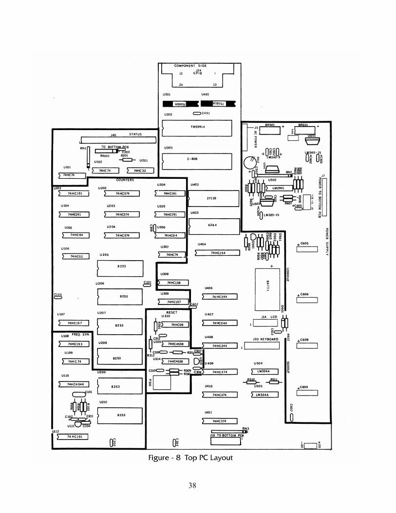
38
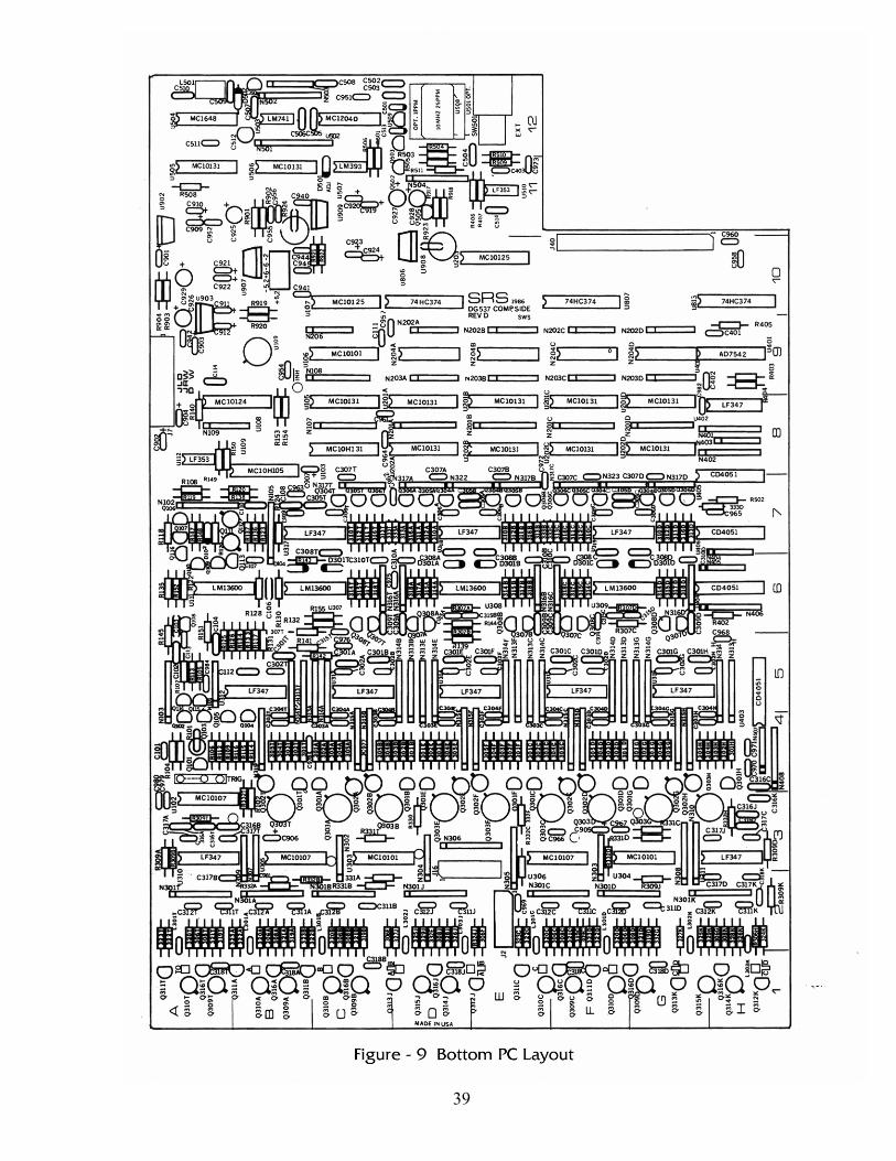
39
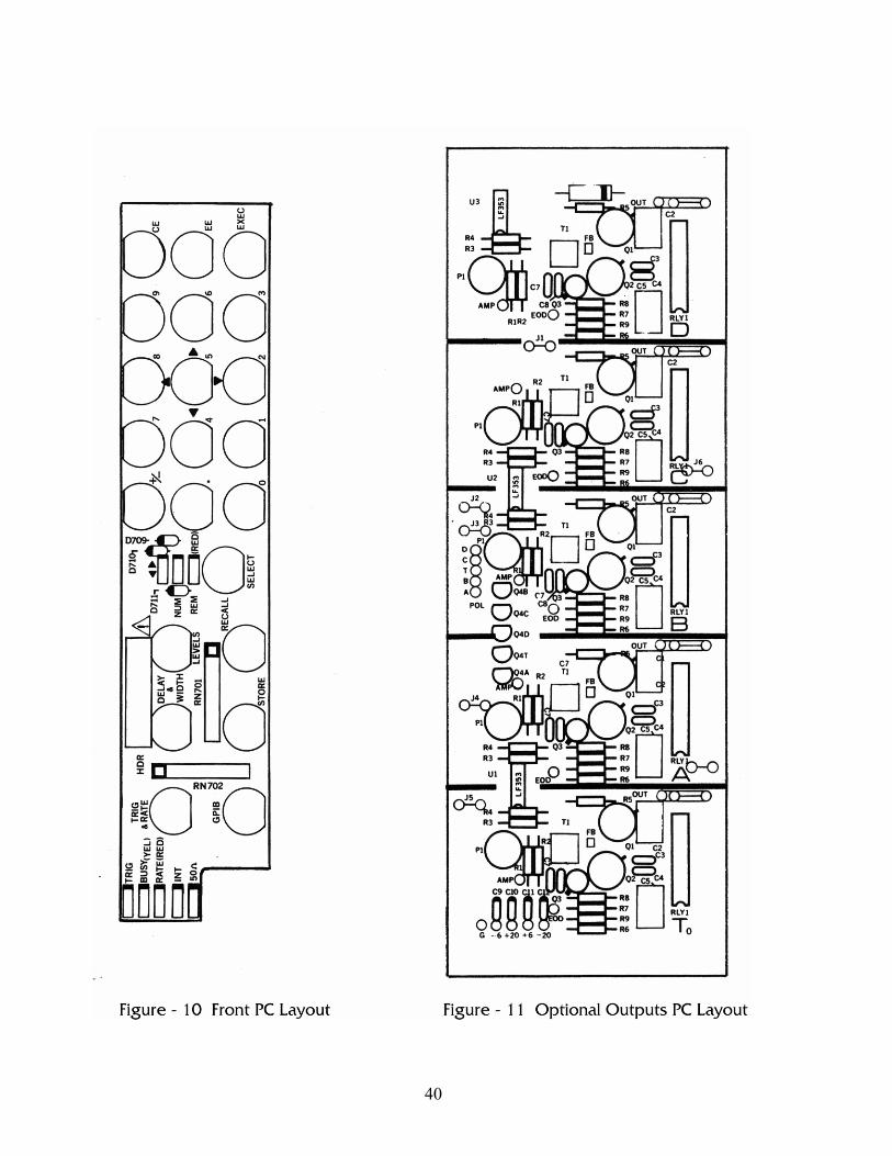
40
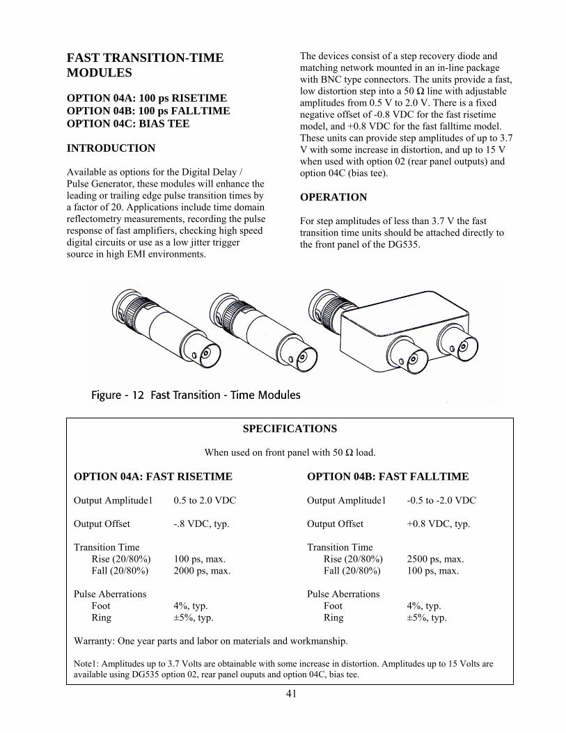
41
FAST TRANSITION-TIME MODULES OPTION 04A: 100 ps RISETIME OPTION 04B: 100 ps FALLTIME OPTION 04C: BIAS TEE INTRODUCTION Available as options for the Digital Delay / Pulse Generator, these modules will enhance the leading or trailing edge pulse transition times by a factor of 20. Applications include time domain reflectometry measurements, recording the pulse response of fast amplifiers, checking high speed digital circuits or use as a low jitter trigger source in high EMI environments.
The devices consist of a step recovery diode and matching network mounted in an in-line package with BNC type connectors. The units provide a fast, low distortion step into a 50 Ω line with adjustable amplitudes from 0.5 V to 2.0 V. There is a fixed negative offset of -0.8 VDC for the fast risetime model, and +0.8 VDC for the fast falltime model. These units can provide step amplitudes of up to 3.7 V with some increase in distortion, and up to 15 V when used with option 02 (rear panel outputs) and option 04C (bias tee). OPERATION For step amplitudes of less than 3.7 V the fast transition time units should be attached directly to the front panel of the DG535.
SPECIFICATIONS
When used on front panel with 50 Ω load.
OPTION 04A: FAST RISETIME OPTION 04B: FAST FALLTIME Output Amplitude1 0.5 to 2.0 VDC Output Amplitude1 -0.5 to -2.0 VDC Output Offset -.8 VDC, typ. Output Offset +0.8 VDC, typ. Transition Time Transition Time Rise (20/80%) 100 ps, max. Rise (20/80%) 2500 ps, max. Fall (20/80%) 2000 ps, max. Fall (20/80%) 100 ps, max. Pulse Aberrations Pulse Aberrations Foot 4%, typ. Foot 4%, typ. Ring ±5%, typ. Ring ±5%, typ. Warranty: One year parts and labor on materials and workmanship. Note1: Amplitudes up to 3.7 Volts are obtainable with some increase in distortion. Amplitudes up to 15 Volts are available using DG535 option 02, rear panel ouputs and option 04C, bias tee.
42
OUTPUT STEPS LESS THAN 2.0 VOLTS The output from the fast transition-time units will have a step amplitude of 1/2 of the programmed output amplitude from the DG535. The offset, which may be adjusted for the best pulse shape on the fast transition, will be about -0.8 VDC for the fast risetime unit, and about +0.8 VDC for the fast fall time unit (.ie. 1/2 of the programmed offset). The offset is critical to the operation of the device: the offset is used to forward bias the step recovery diode (SRD) prior to the pulse output from the DG535. When the pulse from the DG535 begins, the stored carriers in the SRD maintain the conduction in the diode, shunting the output pulse to ground. When the stored carriers are depleted (about 3 ns after the start of the pulse), the diode abruptly stops conduction, creating a very fast transition time step at the output. The offset must be increased when the output amplitude is increased. The offset should be set to about 1.45 v for a 1.0 V amplitude, and to about 1.70 V for a 4.0 V amplitude from the DG535. The offset may be adjusted for the best output pulse shape. If the offset is set too high, the output step will overshoot: if the offset is too
small, the output step will undershoot the final value. OUTPUTS STEPS UP TO 3.7 VOLTS The step size of the output pulse may be increased to about 3.7 VDC by changing the output configuration of the DG535. This configuration will increase the step size and the distortion of the output pulse. In each of these cases, the offset of the DG535's outputs may be adjusted for minimum pulse distortion. Specifying a load impedance of 50 Ω will allow larger pulse amplitudes at the expense of increased ringing after the fast transition. Pulse aberrations after the fast transition will be about 10%, or about 3x larger than the pulse aberrations when a high impedance load is specified. OUTPUT STEPS UP TO 15 VOLTS The fast rise time (option 04A) and fast fall time (option 04B) units may be used with the high voltage rear panel outputs (option 02) to generate step sizes up to 15 V. A bias tee, Option 04C, is required for this mode of operation. The high voltage rear panel outputs are ac coupled hence some accommodation must be made to provide a dc current to forward bias the SRD prior to the output pulse. This current is applied via a bias
SETUP FOR OUTPUT STEPS LESS THAN 2.0 VOLTS
Option 04A, Fast Risetime (All front panel outputs) LOAD= HIGH-Z Internal 50Ω in place VARiable output AMPLITUDE +1 to +4V Output step = AMPLITUDE/2 OFFSET -1.45 to -1.70 V Adjust for best shape Option 04B, Fast Falltime (T0, A, B, C, D only) LOAD = HIGH-Z Internal 50Ω in place VARiable Output AMPLITUDE -1 to -4V Output step = AMPLITUDE/2 OFFSET +1.45 to +1.70 V Adjust for best shape __ __ Option 04B, Fast Falltime (AB, AB, CD, CD) LOAD = HIGH-Z Internal 50Ω in place VARiable Output AMPLITUDE +1 to +4V Output step = AMPLITUDE/2 OFFSET=1.6V-AMPLITUDE Adjust for best shape
SETUP FOR OUTPUT STEPS UP TO 3.7 VOLTS
Option 04A, Fast Risetime (All front panel outputs) LOAD = 50Ω Removes internal 50Ω VARiable outputs AMPLITUDE = 4.0 V OFFSET = -1.15 V Option 04B, Fast Falltime (T0, A, B, C, D only) LOAD = 50Ω Removes internal 50Ω VARiable outputs AMPLITUDE = -4.0 V OFFSET = +1.15 V __ __ Option 04B, Fast Falltime (AB, AB, CD, CD) LOAD = 50Ω Removes internal 50Ω VARiable Outputs AMPLITUDE = 4.0 V OFFSET = 1.15V - AMPLITUDE
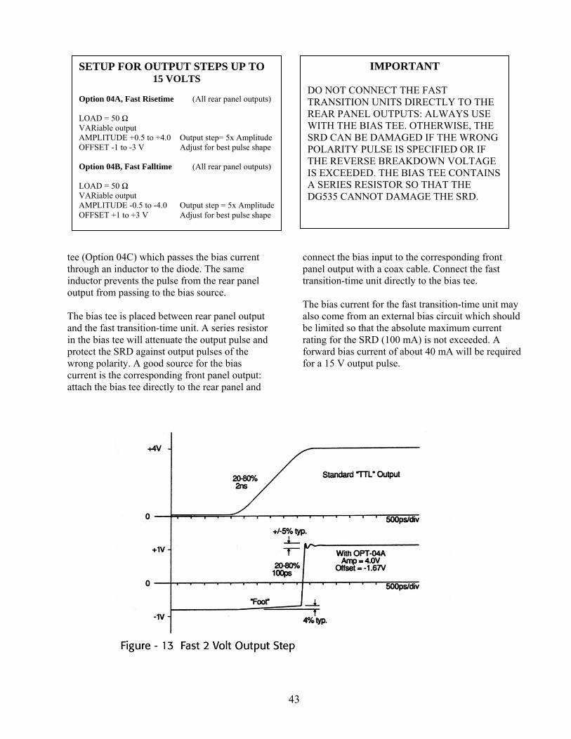
43
tee (Option 04C) which passes the bias current through an inductor to the diode. The same inductor prevents the pulse from the rear panel output from passing to the bias source. The bias tee is placed between rear panel output and the fast transition-time unit. A series resistor in the bias tee will attenuate the output pulse and protect the SRD against output pulses of the wrong polarity. A good source for the bias current is the corresponding front panel output: attach the bias tee directly to the rear panel and
connect the bias input to the corresponding front panel output with a coax cable. Connect the fast transition-time unit directly to the bias tee. The bias current for the fast transition-time unit may also come from an external bias circuit which should be limited so that the absolute maximum current rating for the SRD (100 mA) is not exceeded. A forward bias current of about 40 mA will be required for a 15 V output pulse.
SETUP FOR OUTPUT STEPS UP TO 15 VOLTS
Option 04A, Fast Risetime (All rear panel outputs) LOAD = 50 Ω VARiable output AMPLITUDE +0.5 to +4.0 Output step= 5x Amplitude OFFSET -1 to -3 V Adjust for best pulse shape Option 04B, Fast Falltime (All rear panel outputs) LOAD = 50 Ω VARiable output AMPLITUDE -0.5 to -4.0 Output step = 5x Amplitude OFFSET +1 to +3 V Adjust for best pulse shape
IMPORTANT DO NOT CONNECT THE FAST TRANSITION UNITS DIRECTLY TO THE REAR PANEL OUTPUTS: ALWAYS USE WITH THE BIAS TEE. OTHERWISE, THE SRD CAN BE DAMAGED IF THE WRONG POLARITY PULSE IS SPECIFIED OR IF THE REVERSE BREAKDOWN VOLTAGE IS EXCEEDED. THE BIAS TEE CONTAINS A SERIES RESISTOR SO THAT THE DG535 CANNOT DAMAGE THE SRD.