MODBUS/DeviceNet Master Software Development Guide …pub/@electrical/documents/con… ·...
43
MODBUS/DeviceNet Master Software Development Guide for Network Programmable Model E777, ECIO-DN, ECIO-120-DN, ECOM-DN PG_E777_Modbus_DeviceNet_A1 June 2007
Transcript of MODBUS/DeviceNet Master Software Development Guide …pub/@electrical/documents/con… ·...
MODBUS/DeviceNet Master Software Development Guide for Network Programmable
Model E777, ECIO-DN, ECIO-120-DN, ECOM-DN
PG_E777_Modbus_DeviceNet_A1
June 2007
SOFTWARE DEVELOPMENT GUIDE PAGE 2
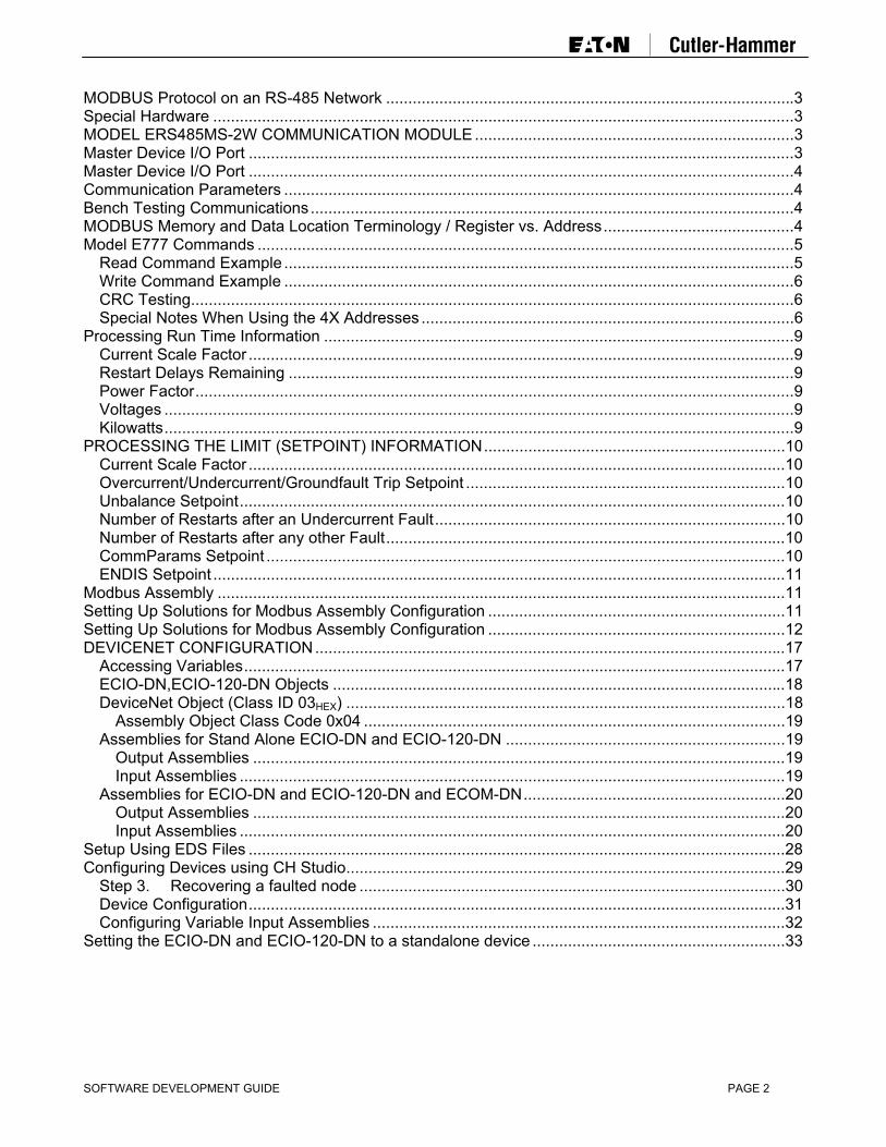
MODBUS Protocol on an RS-485 Network ............................................................................................3 Special Hardware ...................................................................................................................................3 MODEL ERS485MS-2W COMMUNICATION MODULE ........................................................................3 Master Device I/O Port ...........................................................................................................................3 Master Device I/O Port ...........................................................................................................................4 Communication Parameters ...................................................................................................................4 Bench Testing Communications.............................................................................................................4 MODBUS Memory and Data Location Terminology / Register vs. Address...........................................4 Model E777 Commands .........................................................................................................................5
Read Command Example ...................................................................................................................5 Write Command Example ...................................................................................................................6 CRC Testing........................................................................................................................................6 Special Notes When Using the 4X Addresses ....................................................................................6
Processing Run Time Information ..........................................................................................................9 Current Scale Factor ...........................................................................................................................9 Restart Delays Remaining ..................................................................................................................9 Power Factor.......................................................................................................................................9 Voltages ..............................................................................................................................................9 Kilowatts..............................................................................................................................................9
PROCESSING THE LIMIT (SETPOINT) INFORMATION....................................................................10 Current Scale Factor .........................................................................................................................10 Overcurrent/Undercurrent/Groundfault Trip Setpoint ........................................................................10 Unbalance Setpoint...........................................................................................................................10 Number of Restarts after an Undercurrent Fault...............................................................................10 Number of Restarts after any other Fault..........................................................................................10 CommParams Setpoint .....................................................................................................................10 ENDIS Setpoint .................................................................................................................................11
Modbus Assembly ................................................................................................................................11 Setting Up Solutions for Modbus Assembly Configuration ...................................................................11 Setting Up Solutions for Modbus Assembly Configuration ...................................................................12 DEVICENET CONFIGURATION..........................................................................................................17
Accessing Variables..........................................................................................................................17 ECIO-DN,ECIO-120-DN Objects ......................................................................................................18 DeviceNet Object (Class ID 03HEX) ...................................................................................................18
Assembly Object Class Code 0x04 ...............................................................................................19 Assemblies for Stand Alone ECIO-DN and ECIO-120-DN ...............................................................19
Output Assemblies ........................................................................................................................19 Input Assemblies ...........................................................................................................................19
Assemblies for ECIO-DN and ECIO-120-DN and ECOM-DN...........................................................20 Output Assemblies ........................................................................................................................20 Input Assemblies ...........................................................................................................................20
Setup Using EDS Files .........................................................................................................................28 Configuring Devices using CH Studio...................................................................................................29
Step 3. Recovering a faulted node ................................................................................................30 Device Configuration.........................................................................................................................31 Configuring Variable Input Assemblies .............................................................................................32
Setting the ECIO-DN and ECIO-120-DN to a standalone device .........................................................33

SOFTWARE DEVELOPMENT GUIDE PAGE 3
MODBUS MASTER SOFTWARE DEVELOPMENT GUIDE This guide is addressed to systems integrators who will be developing software for a MODBUS master device to communicate with the Model E777 family of products. Experienced programmers should note that Table 1 and Table 3 contain the Model E777 memory maps. The MODBUS master device would typically be a Programmable Logic Controller (PLC) or a Personal Computer (PC) that will communicate with one or more slave devices. A PLC normally would have the MODBUS command protocols and Cyclic Redundancy Check (CRC) word calculation routines built into it, so the programmer would not have to develop them. If programming a Personal Computer, these would have to be developed. If programming a PC, it may be worth noting that it is the responsibility of the master controller to initiate communication. In other words, the master controller must be programmed to periodically poll the slave devices and initiate a request for data or to issue a command to the Model E777 to stop or reset the Model E777’s control relay. When the Model E777 responds with the requested data or confirmation of the stop command, it is the responsibility of the master controller to determine if the information arrived correctly with no communication errors. If there are communication errors or if there is a time-out waiting for a response, it is the responsibility of the master controller to reissue the command to the slave device. If the response arrives correctly, the master controller is then required to further process the data to put it in a form suitable for viewing by an operator.
MODBUS Protocol on an RS-485 Network The Model E777 uses the MODBUS protocol in Remote Terminal Unit (RTU) mode to receive commands and send information as a slave device on an RS-485 network. The RTU mode essentially means that the characters sent between the master and slave devices are binary numbers, not ASCII digits. RS-485 uses a differential voltage signal to represent the zeros and ones. The RS-485 standard allows a single network to contain up to 4000 feet of shielded twisted-pair network cable. The cable only needs to be 22 or 24 gauge to transmit 4000 feet at 9600 baud. Refer to installation instructions for Model ERS485MS-2W for more information. The MODBUS standard allows up to 255 devices on a single network. In a practical sense, it is difficult to scan more than 20 or 30 devices in a timely manner.
Special Hardware Each Model E777 requires a Model ERS485MS-2W Communication Module to connect to the RS-485 network. It is important to recognize that the nine-pin connector on the Model E777 is NOT an RS232 connector! The Communication Module provides electrical isolation from the high voltages present in the Model E777 and it also converts the 5 volt signals from the microcontroller to RS-485 levels.
MODEL ERS485MS-2W COMMUNICATION MODULE The Model ERS485MS-2W Communications Module serves two very important functions. The module electrically isolates the communications network from the high voltages present in the Model E777 and also converts the communications signals from the microcontroller’s 5 volt levels into RS-485 levels. The Model E777 is connected to high AC voltages with a floating ground circuit. As long as there are three balanced line voltages present, the resulting ground level will often be near case ground. However, if one phase is lost or if the line voltages become unbalanced, the floating ground may be as much as 480 volts above the case ground. The Communication Module has two high speed optical isolation chips on the Receive and Transmit pins and a low speed opto-isolator on the Transmit/Receive pin to isolate the communication network from the AC line voltages. In addition, a separate isolated power supply system provides power for the transceiver used for RS-485 level conversion. The Model ERS485MS-2W also provides a power source for a remotely mounted Model ERM-1000. The second function of the Communication Module is to convert the microcontroller signal levels to RS-485 levels. The microcontroller is a CMOS unit with 0 and 5 volt levels. The signals from the microcontroller go through resistors to provide current-limiting before connecting to the 9 pin external connector. Therefore, the 9 pin sub-d connector on the Model E777 provides un-isolated CMOS signals and is NOT RS232 or TTL compatible.
IMPORTANT DO NOT PLUG A MODEM OR ANY OTHER PC-COMPATIBLE SERIAL DEVICE INTO THE 9-PIN CONNECTOR OF THE E777!

SOFTWARE DEVELOPMENT GUIDE PAGE 4
Master Device I/O Port Your MODBUS master device should have an RS-485 port. If your master device only has RS-232 ports, an RS-232 to RS-485 converter will be required. Before ordering a converter, you may need to know if you can program your master device to independently control the RTS line. Some RS-232 to RS-485 converters use the RS-232 signal called RTS (Request-To-Send) to turn on the RS-485 lines before transmitting a command. If your master device cannot control the RTS line, you will need to order an RS-232 to RS-485 converter that automatically turns on the RS-485 line whenever a command is being written.
Communication Parameters The default communication parameters for a standard Model E777 are: 9600 baud EVEN parity 8 data bits 1 stop bit
Bench Testing Communications You can apply ordinary single phase 120VAC power to a 480 volt Model E777 on the L1 and L2 terminals and set the operating parameters. However, you must supply 160VAC if you want to test the communications with the Model ERS485MS-2W connected. If you only have 120 volt power available, you may need to use a 2:1 step up transformer to supply 240VAC to conduct the communications test. Note that the Model E777 will not start with only L1 and L2 connected, but you can read the voltage registers to test the communications.
MODBUS Memory and Data Location Terminology / Register vs. Address The MODBUS standard defines a memory location in terms of registers and addresses. The “register” numbering system starts Xxxxxx1 and goes up to X65536, where the leading X is a reference number that designates a register type. The “address” numbering system starts at 0 rather than 1 and does not contain a prefix. The prefix indicates which read and write functions should be used to get or set the corresponding location. The Modicon MODBUS Protocol Reference Guide refers to these XX references, such as 4X reference for holding registers. However, the MODBUS standard that can be found at www.MODBUS-ida.org does not use these “references”. Older standards and products tend to use a 5-digit numbering system for registers. (Ex: 40,001 for the first holding register) However, other documentation is written using a 6-digit numbering system, which makes sense since MODBUS supports registers up to 65536. (Ex: 400,001 for the first holding register). The “address” numbering system is defined in the standard to describe the message that is actually sent to the physical communications bus. By starting the addresses at 0 rather than 1 and by truncating the register type prefix or reference, the number of usable memory or data locations is maximized. This document will use the terms “address” and “location” interchangeably to refer to the actual address placed on the bus to get the intended piece of data.

SOFTWARE DEVELOPMENT GUIDE PAGE 5
Model E777 Commands The Model E777 will respond to four MODBUS commands.
1. INSTRUCTION CODE 03 Read Holding Registers - to read a block of words The 03 code is used to read data from the Model E777.
2. INSTRUCTION CODE 04 Read Input Registers - to read a block of words The 04 code is used to read data from the Model E777.
3. INSTRUCTION CODE 06 Preset Single Register - to write one value The 06 code is used to send a command to stop the motor attached to the Model E777. The 06 code can also be used to modify the setpoints of the Model E777.
4. INSTRUCTION CODE 16 Preset Multiple Registers (E777 Supports only 1 register write)
The 16 code is used to modify the setpoints of the Model E777. Broadcast is not supported. Read Command Example A typical request for a model E777 would be to ask for the 4 voltages starting at address 22, or 16 hexadecimal, which are the Voltage in Phase C-A, the Voltage in Phase B-C, the Voltage in Phase A-B, and the Average Voltage. In the example below, the values will be returned as 481, 476, 483 and 480 volts for these variables. Assume that the Model E777 has been programmed with a device address of A02. The MODBUS command message from the master device to a slave device would look like: Byte Contents Example (in Hex) 1 Address of Slave Device 02 2 Command to Slave Device 03 3 High Byte of Address 00 (Address of VCA) 4 Low Byte of Address 16 5 High Byte of Number of Words 00 (Read 4 words) 6 Low Byte of Number of Words 04 7 LOW byte of CRC word A5 8 HIGH byte of CRC word FE The above sequence would be a request to read 4 words (8 bytes) starting at address 43. The normal response from the slave device to the master device would look something like: Byte Contents Example (in Hex) 1 Address of Slave Device 02 2 Echo of Command to Slave Device 03 3 Number of Bytes sent back 08 4 High Byte of Word at 002C 01 (VCA = 481) 5 Low Byte of Word at 002C E1 6 High Byte of Word at 002E 01 (VBC = 476) 7 Low Byte of Word at 002E DC 8 High Byte of Word at 0030 01 (VAB = 483) 9 Low Byte of Word at 0030 E3 10 High Byte of Word at 0032 01 (VAVG = 480) 11 Low Byte of Word at 0032 E0 12 LOW byte of CRC word 8A 13 HIGH byte of CRC word 41 The voltage values listed would be values that might be expected from a 480 volt system.
Note: The CRC (Cyclic Redundancy Check) word is sent with the Low byte first followed by the High byte. The CRC bytes are sent in a different order from the order of the Address and Number-Of-Words-To-Send words. The Address and Number-Of-Words-To-Send words are sent with the high byte first followed by the low byte.

SOFTWARE DEVELOPMENT GUIDE PAGE 6
Write Command Example If a Model E777 has been programmed with a device address of A01, the command to turn off the relay would be: Byte Contents Example (in Hex) 1 Address of Slave Device 01 2 Command to Slave Device 06 3 High Byte of Address 00 (Address of COMLINE) 4 Low Byte of Address 65 5 High Byte of Value to write 00 (Sending STOP command) 6 Low Byte of Value to write DD 7 LOW byte of CRC word 59 8 HIGH byte of CRC word 8C The above sequence would be a request to write 1 byte starting at address 101, or 65 hexadecimal, which is the address of the command word, COMLINE. The normal response from the Model E777 is to echo the same byte sequence back to the master device. This is a confirmation that the command was carried out. CRC Testing If you need to test your CRC calculations, you can generate a STOP command exactly like the one above and compare the CRC bytes that your program generates with the CRC bytes listed above. If you set the Model E777’s address to A01 and send the above string, the Model E777 should turn off its relay and the display should show “oFF”. If the first six bytes are exactly like the above sequence, the Model E777 will ONLY respond correctly if the CRC bytes are also exactly like the above sequence. If the Model E777 receives any other CRC bytes, it will assume a communication error occurred and will NOT turn off its relay.
NOTE: If you are using an oscilloscope to capture the sequence of bits that are being transmitted, note that the MODBUS RTU mode specifies that the LEAST significant bit of each byte is transmitted first. Thus, for the sequence above, you would see a Start bit, followed by a high, then low, low, low, then low, low, low, low, followed by the Parity and Stop bits for the first byte (01 hex) sent.
Similarly, the command to reset the same Model E777 would be: Byte Contents Example (in Hex) 1 Address of Slave Device 01 2 Command to Slave Device 06 3 High Byte of Address 00 (Address of COMLINE) 4 Low Byte of Address 65 5 High Byte of Value to write 00 (Sending RESET command) 6 Low Byte of Value to write AA 7 LOW byte of CRC word 19 8 HIGH byte of CRC word AA Again, note the CRC bytes. These STOP and RESET command examples are excellent test commands to verify CRC calculations and communication problems since the only thing that will change in a particular installation is the address of the Model E777 and, of course, the CRC bytes. For example, if the Model E777 has been programmed with device address A11, then the series of bytes would be: Byte Contents Example (in Hex) 1 Address of Slave Device 0B 2 Command to Slave Device 06 3 High Byte of Address 00 (Address of COMLINE) 4 Low Byte of Address 65 5 High Byte of Value to write 00 (Sending RESET command) 6 Low Byte of Value to write AA 7 LOW byte of CRC word 19 8 HIGH byte of CRC word 00 Notice that in this example, only the Address of the Model E777 and the CRC bytes have changed from the series of bytes sent to the Model E777 at device address A01. Special Notes When Using the 4X Addresses Some software packages, such as Human-Machine-Interface (HMI) software packages for PLCs, can only use registers from 400001 to 465536 in the MODBUS 03 and 06 commands. If this is the case, add 400001 to the addresses in the tables to select the start of the data to read. Many of these software packages will automatically subtract the 400001 part of the address before sending the actual address in the MODBUS command.

SOFTWARE DEVELOPMENT GUIDE PAGE 7
Table 1. Run Time Information DeviceNet 16 Bit Modbus
Address C,I,A (Hex) Hex Dec Code and Description Notes
NA
0x01 40002 MAJORVR Major Software Revision
E777 E777-575 E777-LR
E777-575-LR
NA 0x02 40003 MINORVR Minor Software Revision
E777 E777-575 E777-LR
E777-575-LR
0xrr04 0xrr05 0xrr02
0xrr08 NA 0x03 40004 UNITID
Product Code E777
E777-575 E777-LR
E777-575-LR
1 3 11 13
0F,21,01 29,01,BA
0x04 40005 OLSTAT OLSTAT bits
Bit 0: LV detected Bit 1: HV detected Bit 2: VUB detected Bit 3: UC detected
Bit 4: RP detected Bit 5: CUB detected Bit 6: vSP detected Bit 7: cSP detected Bit 8: OC detected Bit 9: GF detected Bit 10: Reserved1
Bit 11: Reserved1 Bit 12: Reserved1
Bit 13: Reserved1
Bit 14: Reserved1
Bit 15: Fault Relay Closed 0F,20,01 29,01,B9
0x05 40006 TRIPRN Trip Reason bits
Bit 0: Man. Reset required Bit 1: Off command issued Bit 2: Tripped on CF Bit 3: Tripped on UC
Bit 4: Tripped on OC Bit 5: Tripped on GF Bit 6: Tripped on CUB Bit 7: Tripped on cSP Bit 8: Reserved1 Bit 9: Reserved1
Bit 10: Reserved1 Bit 11: Reserved1 Bit 12: Reserved1
Bit 13: Reserved1
Bit 14: Reserved1
Bit 15: Reserved1 1. The state of reserved bits is undefined

SOFTWARE DEVELOPMENT GUIDE PAGE 8
Table 1. Run Time Information DeviceNet 16 Bit Modbus
Address C,I,A (Hex) Hex Dec Code and Description Notes
0F,10,01 29,01,74
0x06 40007 LF1 Last Fault
0F,11,01 29,01,75
0x07 40008 LF2 Second to Last Fault
0F,12,01 29,01,76
0x08 40009 LF3 Third to Last Fault
0F,13,01 29,01,77
0x09 40010 LF4 Fourth to Last Fault
Code Definition 0 Cleared 1 Reserved
2 Reserved1
4 Contactor Failure 6 Single Phased Current 7 Ground Fault 8 Current Unbalance 9 Reserved1
10 Overcurrent 11 Undercurrent 12 Reserved1
13 Reserved1 14 Reserved1
15 Reserved1
16 Reserved1 17 Reserved1
18 Reserved1 19 Reserved1
0F,14,01 29,01,AA
0x0A 40011 RD1R Remaining RD1 time
Seconds
0F,15,01 29,01,AB
0x0B 40012 RD2R Remaining RD2 time
Seconds
0F,16,01 29,01,AC
0x0C 40013 RD3R Remaining RD3 time
Seconds
0F,0A,01 2C,01,07 2C,01,6F
0x0D 40014 Capacity Thermal Capacity Remaining
%
0F,1F,01 77,01,08
0x0E 40015 PFANGLE Power factor angle
Degrees
0F,19,01 29,01,B4
0x0F 40016 RTKW Kilowatts
Actual KW=Raw Value/100
0F,05,01 0F,0B,01
0x10 40017 GFCUR Ground Fault Current
Actual GF Amps=Raw Value/Current Scale Factor
0F,03,01 2C,01,0A 2C,01,67
0x11 40018 IC Current in Phase C
Actual Amps=Raw Value/Current Scale Factor
0F,02,01 2C,01,09 2C,01,66
0x12 40019 IB Current in Phase B
Actual Amps=Raw Value/Current Scale Factor
0F,01,01 2C,01,08 2C,01,65
0x13 40020 IA Current in Phase A
Actual Amps=Raw Value/Current Scale Factor
0F,04,01 2C,01,05 2C,01,68
0x14 40021 IAVG Average Current
Actual Amps=Raw Value/Current Scale Factor
0F,0C,01 2C,01,06 2C,01,72
0x15 40022 CUNBAL Current Unbalance measured
%
0F,1C,01 77,01,06
0x16 40023 VCA Voltage from Phase C to Phase A
Volts
0F,1B,01 77,01,05
0x17 40024 VBC Voltage from Phase B to Phase C
Volts
0F,1A,01 77,01,04
0x18 40025 VAB Voltage from Phase A to Phase B
Volts
0F,1D,01 77,01,03
0x19 40026 VAVG Average Voltage
Volts
0F,1E,01 77,01,07
0x1A 40027 VUNBAL Voltage Unbalance
%
1. The state of reserved bits is undefined

SOFTWARE DEVELOPMENT GUIDE PAGE 9
Processing Run Time Information
Current Scale Factor The E777 has a read only scale factor at location 0x79. The value will scale OC, UC, GF and real-time currents. This value will be either 1 or 10 or 100.
Actual Current = Raw Current / Scale Factor
Restart Delays Remaining The restart delay remaining times (RD1R, RD2R, and RD3R) is read directly in seconds.
Power Factor You must take the Cosine of the power factor angle to calculate the Power Factor.
Power Factor= Cos( [power factor angle] ) The power factor angle is read as a value in degrees. If your Cosine function requires the angle to be expressed in radians, you can convert degrees to radians by multiplying by (Pi / 180.0)
Voltages The voltages read correctly as integer values. No calculating is necessary to display the same value that the Model E777 displays.
Kilowatts The kilowatts need to be divided by 100.
Kilowatts= [KW reading] / 100

SOFTWARE DEVELOPMENT GUIDE PAGE 10
PROCESSING THE LIMIT (SETPOINT) INFORMATION
Current Scale Factor The E777 has a read only scale factor at location 0x79. The value will scale GF, OC, UC setpoints. This value will be either 1 or 10 or 100 depending on the size. The E777 has a size parameter that determines the current ranges and also the scale factor.
Table 2. Size information Size Network Value Current Scale Factor 00 0 100 0 1 100 1 2 10 2 3 10 3 4 10 4 5 1 5 6 1 6 7 1
Overcurrent/Undercurrent/Groundfault Trip Setpoint The overcurrent, undercurrent, and Groundfault setpoints are scaled by the scale factor of the device. To write these setpoints first read the scale factor and multiply by actual amps and write this value. A read of these setpoint must be divided by the scale factor to get actual amps
Writing OC/UC/GF
Scale factor=10 Actual Amps=10.1A Value to Write=Actual Amps*Scale Factor=101
Reading OC/UC/GF
Value Read/Scale Factor=Actual Amps Scale factor=10 Value Read=101 Actual Amps=10.1A
Note: Network value of 255 for the Groundfault setpoint will turn Groundfault protection off. Network value of 0 for the Undercurrent setpoint will turn Undercurrent protection off.
Unbalance Setpoint
If either the voltage (VUB) or current (CUB) unbalance limit is 255 (0xFF), the unbalance limit is turned OFF.
Number of Restarts after an Undercurrent Fault If #RU reads 255, the unit will automatically restart after all undercurrent faults. (Note that if #RU is zero, the unit will not start after an undercurrent fault until the Reset button is pressed or a RESET command is sent to the Model E777.)
Number of Restarts after any other Fault The #RF value contains certain bit settings. If Bit 0 (the least significant bit) is set, the Number of Restarts will apply to over current faults. Bits 1 through 3 represent the Number of Restarts. A value of 0 to 4 is the Number of Restarts. If the value is 5, the unit will automatically restart after any other fault. As an example, if #RF contains the decimal value 11, it represents the bit pattern “0 0 0 0 1 0 1 1”. This means that the unit will automatically start after other faults, including over current.
CommParams Setpoint The Comm. Parameters setpoint allows the user to set the communication settings for communicating with the E777. This register is composed of 3 bits:
Bit 0: 0=Communicate with parity
1=Communicate with parity
Bit 1: 0=Communicate with odd parity 1=Communicate with even parity Bit 2: 0=Communicate at 9600 Baud 1=Communicate at 19200 Baud Immediately after this register is written communication will continue at the new settings.

SOFTWARE DEVELOPMENT GUIDE PAGE 11
ENDIS Setpoint This register allows the user to disable a trip feature without changing the setpoint of that trip. In this registers are 8 bits to control individual trip setpoints. If a trip is disabled with this register, the front panel will show the disabled value for that setpoint even though the value of the setpoint is preserved. If the trip setpoint is disabled from the front panel and the user enables the trip with this register, the enable will have no effect, and the trip will still be disabled.
Bit 0: 0 = GF trip disabled 1 = GF trip enabled Bit 1: 0 = VUB trip disabled 1 = VUB trip enabled Bit 2: 0 = CUB trip disabled 1 = CUB trip enabled Bit 3: 0 = UC trip disabled 1 = UC trip enabled Bit 4: Reserved Bit 5: Reserved Bit 6: Reserved Bit 7: Reserved Bit 8: Reserved
Modbus Assembly The Modbus assembly allows the master controller to read setpoints and real-time data in any order independently of the published memory map. To configure the assemblies, write the memory map location to locations 0x2153-0x2190. The parameters that can be entered into MBAssem500WrdXX can be found in tables 1 and 3. The value entered into each parameter is the Modbus address of the parameter that the user desires to view. Figure 2 shows the user entered parameter 123,13,20,25,14,15,4,5,122,19,18; when the user does a read of 0x500 for 11 words. The data that is returned will be Motor Run Hours, Thermal Capacity Remaining, Average Current, Average Voltage, Power Factor Angle, Actual Kilowatts, OLSTAT,TRIPRN, Network Status, Current in Phase A, Current in Phase B respectively. Before Modbus assembly parameters can be changed bit Allow Modbus Assembly Edit of NETST must be set See Figure 1.
Figure 2-Modbus Variable Assembly
Figure 1-Network Status Bits

SOFTWARE DEVELOPMENT GUIDE PAGE 12
Setting Up Solutions for Modbus Assembly Configuration Step 1. Start Solutions Step 2. Select Modbus RTU from the Select Network Connection Type dialog box (see Figure 3)
Figure 3-Network Connection Step 3. Click Auto Detect Units on left hand navigation pane (see Figure 4-Empty Network View)
Figure 4-Empty Network View
Step 3

SOFTWARE DEVELOPMENT GUIDE PAGE 13
Step 4. Click the desired device to edit the device parameters (see Figure 5)
Figure 5-Network View

SOFTWARE DEVELOPMENT GUIDE PAGE 14
Table 3. Writing Limit (Setpoint) Values DeviceNet 16 Bit Modbus Address C,I,A (Hex) Hex Register Code and Description Range Default NA 0x65 40102 ComLine
Command Line 0x44: Enable Network Programming 0x55: Disable Network Programming 0x66: Clear Motor Run Hours 0x77: Clear Last Fault 0x88: Enable Network Watchdog Timer 0x99: Disable Network Watchdog Timer 0xAA: Reset Model E777 0xDD: Turn Model E777 OFF
0
NA 0x66 40103 # of loops through E777 CT windows 2C,01,89 0x67 40104 GF
Ground Fault Setpoint Size
00 0 1 2 3 4 5 6
Raw Value=Actual Amps/Scale Factor Actual Amps Range .15-1.00 Amps, Off (255) .3-2.00 Amps, Off (255) 1.5-10 Amps, Off (255) 3-20 Amps, Off (255) 3-20 Amps, Off (255) 9.00-60 Amps, Off (255) 18-120 Amps, Off (255) 36-240 Amps, Off (255)
E777=10 E777-LR=1.0
2C,01,93 0x68 40105 UC Under Current Setpoint
Size 00
0 1 2 3 4 5 6
Raw Value=Actual Amps/Scale Factor Actual Amps Range Off (0), .5-5.9 Amps Off (0), 1-11.8 Amps Off (0), 3.3-33 Amps Off (0), 5-50 Amps Off (0), 10-100 Amps Off (0), 30-151 Amps Off (0), 60-302 Amps Off (0), 120-604 Amps
E777=35 E777-LR=3.5
2C,01,03 0x69 40106 OC Over Current Setpoint
Size 00
0 1 2 3 4 5 6
Raw Value=Actual Amps/Scale Factor Actual Amps Range 1-6.5 Amps 2-13 Amps 6.6-35 Amps 10-52.5 Amps 20-105 Amps 60-155 Amps 120-311 Amps 240-622 Amps
E777=60 E777-LR=6
2C,01,97 0x6A 40107 CUB Current Unbalance Setpoint
2-25 %,Off (255) 7
2C,01,04 2C,01,81
0x6B 40108 TC Trip Class
Trip Class Value 5 5 10 10 15 15 20 20 30 30 J5 133 J10 138 J15 143 J20 148 J30 158
10
77,01,14 0x6C 40109 LV Low Vo l tage
E777 E777-575
170-524 Volts 450-649 Volts
200 450
77,01,15 0x6D 40110 HV High Voltage
E777 777-575
172-528 Volts 451-660 Volts
500 600
1. Do not write reserved bits

SOFTWARE DEVELOPMENT GUIDE PAGE 15
Table 3. Writing Limit (Setpoint) Values DeviceNet 16 Bit Modbus Address C,I,A (Hex) Hex Register Code and Description Range Default 77,01,16 0x6E 40111 VUB
Voltage Unbalance Setpoint 2-15 %,Off (255) 6
29,01,AD 0x6F 40112 RD1 Rapid Cycling Restart Delay
0-500 seconds 10
29,01,AE 0x70 40113 RD2 Restart Delay after OC fault
2-500 seconds 8
29,01,AF 0x71 40114 RD3 Restart Delay after UC fault
2-500 seconds, A (65535) 20
2C,01,92 0x72 40115 UCTD Under Current Trip Delay
2-60 seconds 5
29,01,B0 0x73 40116 #RU Number of restarts after UC fault
0, 1, 2, 3, 4, A (automatic) RU Values 0–4 0–4 A 255
1
29,01,82 29,01,B1
0x74 40117 #RF Number of restarts after OC, cSP, CUB, LCV fault
0, 1, oc1, 2, oc2, 3, oc3, 4, oc4, A, ocA 0 = manual, A = continuous, oc = automatic restart after RD2 expires RF Value Decimal Value 0 1 1 2 oc1 3 2 4 oc2 5 3 6 oc3 7 4 8 oc4 9 A 10 ocA 11
OC1
NA 0x75 40118 ADDR Modbus device address
1-255 1
NA 0x76 40119 ComParam Communication Parameter Bits
Communications Value 9600,N,1 0x00 9600,E,1 0x03 9600,O,1 0x01 19200,N,1 0x04 19200,E,1 0x07 19200,O,1 0x05
9600,E,1
29,01,7C 0x77 40120 ENDIS Enable/Disable bits
Bit 0: GF Trip Enabled Bit 1: VUB Trip Enabled Bit 2: CUB Trip Enabled Bit 3: UC Trip Enabled Bit 4: Reserved1
Bit 5: Reserved1
Bit 6: Reserved1
Bit 7: Reserved1
15
NA 0x78 40121 Contactor Size Size Value 00 0 0 1 1 2 2 3 3 4 4 5 5 6 6 7
E777=3 E777-LR=00
2C,01,64 0x79 40122 Current Scale Factor 1,10,100 Read Only NA 0x7A 40123 NETST
Network Status bits Bit 0: Network Watchdog Enabled Bit 1: Network Program Disabled Bit 2: Front panel locked Bit 3: Reserved1
Bit 4: Allow Modbus Assembly Edit Bit 5: Reserved1
Bit 6: Reserved1
Bit 7: Reserved1
0
1. Do not write reserved bits

SOFTWARE DEVELOPMENT GUIDE PAGE 16
Table 3. Writing Limit (Setpoint) Values DeviceNet 16 Bit Modbus Address C,I,A (Hex) Hex Register Code and Description Range Default 29,01,64 0x7B 40124 MRH
Motor Run Hours 0-65535 Hours 0
NA 0x2153 48532 MBAssebmly500Wrd0 0-255 123 NA 0x2154 48533 MBAssebmly500Wrd1 0-255 13 NA 0x2155 48534 MBAssebmly500Wrd2 0-255 20 NA 0x2156 48535 MBAssebmly500Wrd3 0-255 25 NA 0x2157 48536 MBAssebmly500Wrd4 0-255 14 NA 0x2158 48537 MBAssebmly500Wrd5 0-255 15 NA 0x2159 48538 MBAssebmly500Wrd6 0-255 4 NA 0x215A 48539 MBAssebmly500Wrd7 0-255 5 NA 0x215B 48540 MBAssebmly500Wrd8 0-255 122 NA 0x215C 48541 MBAssebmly500Wrd9 0-255 19 NA 0x215D 48542 MBAssebmly500Wrd10 0-255 18 NA 0x215E 48543 MBAssebmly500Wrd11 0-255 17 NA 0x215F 48544 MBAssebmly500Wrd12 0-255 16 NA 0x2160 48545 MBAssebmly500Wrd13 0-255 21 NA 0x2161 48546 MBAssebmly500Wrd14 0-255 26 NA 0x2162 48547 MBAssebmly500Wrd15 0-255 24 NA 0x2163 48548 MBAssebmly500Wrd16 0-255 23 NA 0x2164 48549 MBAssebmly500Wrd17 0-255 22 NA 0x2165 48550 MBAssebmly500Wrd18 0-255 10 NA 0x2166 48551 MBAssebmly500Wrd19 0-255 11 NA 0x2167 48552 MBAssebmly500Wrd20 0-255 12 NA 0x2168 48553 MBAssebmly500Wrd21 0-255 6 NA 0x2169 48554 MBAssebmly500Wrd22 0-255 7 NA 0x216A 48555 MBAssebmly500Wrd23 0-255 8 NA 0x216B 48556 MBAssebmly500Wrd24 0-255 9 NA 0x216C 48557 MBAssebmly500Wrd25 0-255 3 NA 0x216D 48558 MBAssebmly500Wrd26 0-255 2 NA 0x216E 48559 MBAssebmly500Wrd27 0-255 1 NA 0x216F 48560 MBAssebmly500Wrd28 0-255 102 NA 0x2170 48561 MBAssebmly500Wrd29 0-255 103 NA 0x2171 48562 MBAssebmly500Wrd30 0-255 104 NA 0x2172 48563 MBAssebmly500Wrd31 0-255 106 NA 0x2173 48564 MBAssebmly500Wrd32 0-255 107 NA 0x2174 48565 MBAssebmly500Wrd33 0-255 108 NA 0x2175 48566 MBAssebmly500Wrd34 0-255 109 NA 0x2176 48567 MBAssebmly500Wrd35 0-255 110 NA 0x2177 48568 MBAssebmly500Wrd36 0-255 111 1. Do not write reserved bits

SOFTWARE DEVELOPMENT GUIDE PAGE 17
DEVICENET CONFIGURATION
The CIO-DN DeviceNet I/O Module can be configured using a software tool such as CHStudio or SymCom’s Solutions software. An EDS (electronic data sheet) file is required with each software tool to provide the location, value and size of the device’s configurable attributes.
Accessing Variables Variables on the node are accessed using a Path, which is composed of:
• The Class ID • The Instance ID • The Attribute ID
The classes available in the solid state overload relay are grouped into three parts: • Classes required for all equipment connected to the DeviceNet network, whatever their functionality • Classes relating to the overload relay profile, as defined by ODVA • Classes relating to the E777 overload relay, allowing access to all internal variables: configuration, adjustment,
monitoring, etc.

SOFTWARE DEVELOPMENT GUIDE PAGE 18
ECIO-DN,ECIO-120-DN Objects Table 4. Class Attributes (Class ID 01hex) At t r ibute ID Access Rule Name Data Type Va lue Deta i ls 1 Get Rev is ion U INT 1 - -
Table 5. ID Class (Class ID 01hex) At t r ibute ID Access Rule Name Data Type Va lue Deta i ls 1 GET Vendor ID U INT 68 Cu t le r -Hammer , Inc . 2 GET Produc t
Type U INT 3
7 Moto r Over load Genera l Purpose D isc re te I /O*
3 GET Produc t Code
U INT Product Code Over load Type S ize I /O Module 16129 E777-LR 00 ECOM-DN 16130 E777-LR 0 ECOM-DN 16131 E777 1 ECOM-DN 16132 E777 2 ECOM-DN 16133 E777 3 ECOM-DN 16134 E777-LR 4 ECOM-DN 16135 E777-LR 5 ECOM-DN 16136 E777-LR 6 ECOM-DN 16145 E777-575-LR 00 ECOM-DN 16146 E777-575-LR 0 ECOM-DN 16147 E777-575 1 ECOM-DN 16148 E777-575 2 ECOM-DN 16149 E777-575 3 ECOM-DN 16150 E777-575-LR 4 ECOM-DN 16151 E777-575-LR 5 ECOM-DN 16152 E777-575-LR 6 ECOM-DN 16161 E777-LR 00 ECIO-DN 16162 E777-LR 0 ECIO-DN 16163 E777 1 ECIO-DN 16164 E777 2 ECIO-DN 16165 E777 3 ECIO-DN 16166 E777-LR 4 ECIO-DN 16167 E777-LR 5 ECIO-DN 16168 E777-LR 6 ECIO-DN 16177 E777-575-LR 00 ECIO-DN 16178 E777-575-LR 0 ECIO-DN 16179 E777-575 1 ECIO-DN 16180 E777-575 2 ECIO-DN 16181 E777-575 3 ECIO-DN 16182 E777-575-LR 4 ECIO-DN 16183 E777-575-LR 5 ECIO-DN 16184 E777-575-LR 6 ECIO-DN
Rev is ion Ma jo r Rev i s ion
USINT 4 GET
Mino r Rev i s ion
USINT
5 GET S ta tus WORD 6 GET Ser ia l
Number UDINT
7 GET Name SHORT_STRING 8 GET S ta te USINT * App l i es to ECIO-DN, ECIO-120-DN
DeviceNet Object (Class ID 03HEX) The DeviceNet Object provides the status and configuration of a DeviceNet node.
Table 6. Class Attributes (Class ID 03hex) At t r ibute ID Access Rule Name Data Type Va lue Deta i ls 1 Get Rev is ion U INT 1 - - 2 Ge t Max Ins tances U INT 1 1 de f ined ins tance

SOFTWARE DEVELOPMENT GUIDE PAGE 19
Table 7. Instance Attributes (Class ID 03hex) At t r ibute ID Access Rule Name Data Type Va lue Deta i ls 1 Get /Se t MAC ID USINT 0 -63 Re f = 63 2 Ge t /Se t Baud ra te USINT 0 -2 0 = 125k
1 = 250 k 2 = 500 k
3 Ge t /Se t BOI (BusOf f i n te r rup t )
BOOL - - Upon BusOf f event : 0 : CAN componen t remains i n BusOf f 1 : Component i s rese t—communica t ion resumes
4 Ge t /Se t BusOf f coun te r USINT 0 -255 Number o f occur rences o f BusOf f s ta te 5 Ge t A l l oca t i on
in fo rmat ion BYTE USINT
- - 0 -63
A l l oca t i on cho ice Mas te r address (255 no t a l l oca ted )
Table 8. Class Service (Class ID 03hex) Service Code Service Name Descr ip t ion OE h e x Ge t_At t r i bu te_S ing le Read an a t t r i bu te
Table 9. Instance Service (Class ID 03hex) Service Code Service Name Descr ip t ion OE h e x Ge t_At t r i bu te_S ing le Read an a t t r i bu te 10 h e x Se t_At t r i bu te_S ing le Wr i te an a t t r i bu te 4B h e x A l l oca te Mas te r /S lave Connec t i on Set A l l oca t i on connec t ion mas te r / s lave 4C h e x Re lease Mas te r /S lave Connec t i on Set Re lease connec t ion mas te r / s lave
Assembly Object Class Code 0x04
Assemblies for Stand Alone ECIO-DN and ECIO-120-DN Table 10 Table 11. Bit Definition Input Descr ip t ion
0 Inpu t 1 open In 1 1 Inpu t 1 c losed 0 Inpu t 2 open In 2 1 Inpu t 2 c losed 0 Inpu t 3 open In 3 1 Inpu t 3 c losed 0 Inpu t 4 open In 4 1 Inpu t 4 c losed 0 Ou tpu t A open Out A 1 Ou tpu t A c losed 0 Ou tpu t B open Out B 1 Ou tpu t B c losed
* App l i es to ECIO-DN, ECIO-120-DN
Output Assemblies Table 12. Assembly Object Class Instance 32 B i t 7 B i t 6 B i t 5 B i t 4 B i t 3 B i t 2 B i t 1 B i t 0 Ou t B* Ou t A* * Applies to ECIO-DN, ECIO-120-DN
Input Assemblies Table 13. Output Assembly Object Class Instance 3 B i t 7 B i t 6 B i t 5 B i t 4 B i t 3 B i t 2 B i t 1 B i t 0 I n 4 * In 3 * In 2 * In 1 * * Applies to ECIO-DN, ECIO-120-DN

SOFTWARE DEVELOPMENT GUIDE PAGE 20
Assemblies for ECIO-DN and ECIO-120-DN and ECOM-DN
Output Assemblies
Output Assemblies allow control of the ECOM-DN, ECIO-DN, ECIO-120-DN using a polled message. These assemblies allow the ECIO-DN and ECIO-120-DN to control the Fault relay on the E777 and A and B relays.
Table 14. Bit Definition Output Descr ip t ion
0 No change Fau l t Rese t 1 Rese t fau l t re lay 0 Open ou tpu t A re lay Ou tA* 1 C lose ou tpu t A re lay 0 Open ou tpu t B re lay Ou tB* 1 C lose ou tpu t B re lay
* App l i es to ECIO-DN, ECIO-120-DN
Table 15. Output Assembly Object Class Instance 1 B i t 7 B i t 6 B i t 5 B i t 4 B i t 3 B i t 2 B i t 1 B i t 0 Ou t A* * Applies to ECIO-DN, ECIO-120-DN
Table 16. Output Assembly Object Class Instance 2 B i t 7 B i t 6 B i t 5 B i t 4 B i t 3 B i t 2 B i t 1 B i t 0 Fau l t Rese t
Table 17. Output Assembly Object Class Instance 3 Bi t 7 B i t 6 B i t 5 B i t 4 B i t 3 B i t 2 B i t 1 B i t 0 Fau l t Rese t Ou t A* * Applies to ECIO-DN, ECIO-120-DN
Table 18. Output Assembly Object Class Instance 4 B i t 7 B i t 6 B i t 5 B i t 4 B i t 3 B i t 2 B i t 1 B i t 0 Ou t B* Ou t A* * Applies to ECIO-DN, ECIO-120-DN
Table 19. Output Assembly Object Class Instance 5 B i t 7 B i t 6 B i t 5 B i t 4 B i t 3 B i t 2 B i t 1 B i t 0 Fau l t Rese t Ou t B* Ou t A* * Applies to ECIO-DN, ECIO-120-DN
Input Assemblies Table 20. Bit Definitions I/O Point Description
0 Fault relay open Fault Relay 1 Fault relay closed
0 Output A is open Out A* 1 Output A is closed 0 Output B is open Out B* 1 Output B is closed 0 Input 1 open In 1* 1 Input 1 closed 0 Input 2 open In 2* 1 Input 2 closed 0 Input 3 open In 3* 1 Input 3 closed 0 Input 4 open In 4* 1 Input 4 closed 0 Overload is not faulted Faulted 1 Overload is faulted 0 No Pending Trip Warning 1 Pending Trip
* Applies to ECIO-DN, ECIO-120-DN Table 21. Input Assembly Object Class Instance 50 Bit 7 Bit 6 Bit 5 Bit 4 Bit 3 Bit 2 Bit 1 Bit 0 Faulted

SOFTWARE DEVELOPMENT GUIDE PAGE 21
Table 22. Input Assembly Object Class Instance 51 Bit 7 Bit 6 Bit 5 Bit 4 Bit 3 Bit 2 Bit 1 Bit 0 Warning Faulted Table 23. Input Assembly Object Class Instance 106 Bit 7 Bit 6 Bit 5 Bit 4 Bit 3 Bit 2 Bit 1 Bit 0 In2* In1* OutA* Warning Faulted * Applies to ECIO-DN, ECIO-120-DN Table 24. Input Assembly Object Class Instance 107 Bit 7 Bit 6 Bit 5 Bit 4 Bit 3 Bit 2 Bit 1 Bit 0 In4* In3* In2* In1* Faulted Out B* Out A* * Applies to ECIO-DN, ECIO-120-DN
The ECIO-xxx-DN supports two custom input assemblies. These assemblies are configured by selecting parameters. For input assembly 100, program attributes 7-10 of Class 0xB4 by selecting parameter instances from the Parameter Object Table. To end the list, program “0” for the parameter instance. The process is the same for input assembly 150, except attributes 25-74 of Class 0xB4 are used.
Table 25. Connection Object Class Code 0x05 At t r ibute ID Access Rule Name Data Type Va lue1 GET Rev is ion U INT 1
Table 26. Connection Object--Class Code 0x05, Instance 1 Explicit At t r ibute ID Access Rule Name Data Type Va lue 1 GET S ta te USINT 0 = Nonex is ten t
1 = Con f igu r ing 3 = Es tab l i shed 4 = T imed Out
2 GET Ins tance t ype USINT 0 = Exp l i c i t 3 GET Transpor t c lass t r i gger BYTE - - 4 GET Produced connec t i on ID U INT 10xxxxxx011
Xxxxxx = Node address
5 GET Consumed connec t i on ID U INT 10xxxxxx011 Xxxxxx = Node address
6 GET In i t i a l comm. cha rac te r i s t i cs BYTE - - 7 GET Produced connec t i on s i ze U INT 8 8 GET Consumed connec t ion s i ze U INT 7 9 GET/SET Expec ted packe t ra te U INT - - 12 GET/SET Watchdog t imeou t ac t i on USINT - - 13 GET Produced connec t i on pa th leng th U INT - - 14 GET Produced connec t i on pa th EPATH - - 15 GET Consumed connec t ion pa th leng th U INT - - 16 GET Consumed connec t ion pa th EPATH - -
Table 27. Connection Object Class Code 0x05 At t r ibute ID Access Rule Name Data Type Va lue1 GET Rev is ion U INT 1
Table 28. Connection Object--Class Code 0x05, Instance 2 Polled At t r ibute ID Access Rule Name Data Type Value GET S ta te USINT 0 = Nonex is ten t
1 = Con f igu r ing 3 = Es tab l i shed 4 = T imed Out
2 GET Ins tance t ype USINT 1 = I /O 3 GET Transpor t c lass t r i gger BYTE - -
4 GET Produced connec t i on ID U INT 10xxxxxx011 xxxxxx = Node address
5 GET Consumed connec t ion ID U INT 10xxxxxx011 xxxxxx = Node address
6 GET In i t i a l comm. cha rac te r i s t i cs BYTE - - 7 GET Produced connec t i on s i ze U INT 1 -50 8 GET Consumed connec t ion s i ze U INT 0 -8

SOFTWARE DEVELOPMENT GUIDE PAGE 22
Table 28. Connection Object--Class Code 0x05, Instance 2 Polled At t r ibute ID Access Rule Name Data Type Value 9 GET/SET Expec ted packe t ra te U INT - - 12 GET/SET Watchdog t imeou t ac t i on USINT - - 13 GET Produced connec t i on pa th leng th U INT - - 14 GET Produced connec t i on pa th EPATH - - 15 GET Consumed connec t ion pa th leng th U INT - - 16 GET Consumed connec t ion pa th EPATH - -
Table 29. Discrete Input Class Code 0x08 At t r ibute ID Access Rule Name Data Type Va lue1 GET Rev is ion U INT 1
Table 30. Discrete Input Point Object – Class Code 0x08 Ins tance At t r ibute Services Var iab le Type Descr ip t ion Notes 1 3 GET BOOL Inpu t 1 * 1=C losed , 0=Open 2 3 GET BOOL Inpu t 2 * 1=C losed , 0=Open 3 3 GET BOOL Inpu t 3 * 1=C losed , 0=Open 4 3 GET BOOL Inpu t 4 * 1=C losed , 0=Open * Applies to ECIO-DN, ECIO-120-DN
Table 31. Discrete Output Class Code 0x09 At t r ibute ID Access Rule Name Data Type Va lue1 GET Rev is ion U INT 1
Table 32. Discrete Output Point Object – Class Code 0x09 Ins tance At t r ibute Services Var iab le Type Descr ip t ion Notes 1 3 GET BOOL Fau l t Re lay 1=C losed , 0=Open 2 3 GET/SET BOOL Outpu t A* 1=C losed , 0=Open 3 3 GET/SET BOOL Outpu t B* 1=C losed , 0=Open * Applies to ECIO-DN, ECIO-120-DN
Table 33. Parameter Object – Class 0x0F At t r ibute ID Access Rule Name Data Type Va lue1 GET Rev is ion U INT 1
Table 34. Parameter Object – Class 0x0F, All Instances At t r ibute ID Access Rule Name Data Type Value 1 GET Va lue — Ac tua l va lue o f pa ramete r 2 GET L ink Pa th S i ze USINT 6 3 GET L ink Pa th U INT Depends on ins tance 4 GET Desc r ip to r U INT Depends on ins tance 5 GET Da ta t ype U INT Depends on ins tance 6 GET Da ta s i ze U INT 2
Table 35. Parameter Object – Class 0x0F, Attribute 1 = Value Instances 1–34 Ins tance Access Rule Name Data Type Value 1 GET L1 cu r ren t * 10 U INT Cur ren t * 10 2 GET L2 cu r ren t * 10 U INT Cur ren t * 10 3 GET L3 cu r ren t * 10 U INT Cur ren t * 10 4 GET Average cu r ren t * 10 U INT Cur ren t * 10 5 GET Ground fau l t cu r ren t * 10 U INT Cur ren t * 10 6 GET L1 cu r ren t (%OC) U INT % 7 GET L2 cu r ren t (%OC) U INT % 8 GET L3 cu r ren t (%OC) U INT % 9 GET Avg. cu r ren t (%OC) U INT % 10 GET % Therma l capac i t y rema in ing U INT % 11 GET Ground fau l t cu r ren t U INT Cur ren t * A t t r 100 12 GET Cur ren t unba lance (%) U INT % 13 GET OL t ime to rese t U INT — 1. Do not write reserved bits * App l i es to ECIO-DN, ECIO-120-DN
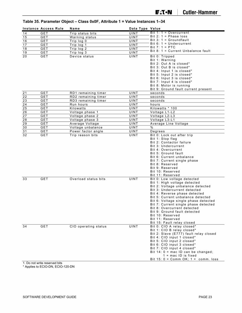
SOFTWARE DEVELOPMENT GUIDE PAGE 23
Table 35. Parameter Object – Class 0x0F, Attribute 1 = Value Instances 1–34 Ins tance Access Rule Name Data Type Value 14 GET Tr ip s ta tus b i t s U INT 15 GET Warn ing s ta tus U INT 16 GET Tr ip l og 0 U INT 17 GET Tr ip l og 1 U INT 18 GET Tr ip l og 2 U INT 19 GET Tr ip l og 3 U INT
B i t 1 : 1 = Overcu r ren t B i t 2 : 1 = Phase loss B i t 3 : 1 = Ground fau l t B i t 6 : 1 = Undercu r ren t B i t 7 : 1 = PTC B i t 8 : 1 = Cur ren t Unba lance fau l t
20 GET Dev ice s ta tus U INT B i t 0 : T r ipped B i t 1 : Warn ing B i t 2 : Out A i s c losed* B i t 3 : Out B i s c losed* B i t 4 : I npu t 1 i s c losed* B i t 5 : I npu t 2 i s c losed* B i t 6 : I npu t 3 i s c losed* B i t 7 : I npu t 4 i s c losed* B i t 8 : Mo to r i s runn ing B i t 9 : Ground fau l t cu r ren t p resen t
21 GET RD1 remain ing t imer U INT seconds 22 GET RD2 remain ing t imer U INT seconds 23 GET RD3 remain ing t imer U INT seconds 24 GET Run hours U INT hours 25 GET K i lowa t t s U INT K i lowa t t s * 100 26 GET Vo l tage phase 1 U INT Vo l tage L1-L2 27 GET Vo l tage phase 2 U INT Vo l tage L2-L3 28 GET Vo l tage phase 3 U INT Vo l tage L3-L1 29 GET Average Vo l tage U INT Average L ine Vo l tage 30 GET Vo l tage unba lance U INT % 31 GET Power fac to r ang le U INT Degrees 32 GET Tr ip reason b i ts U INT B i t 0 : Lock ou t a f te r t r i p
B i t 1 : S top f lag B i t 2 : Con tac to r fa i l u re B i t 3 : Undercu r ren t B i t 4 : Overcur ren t B i t 5 : Ground fau l t B i t 6 : Cur ren t unba lance B i t 7 : Cur ren t s ing le phase B i t 8 : Reserved B i t 9 : Reserved B i t 10 : Reserved B i t 11 : Reserved
33 GET Over load s ta tus b i ts U INT B i t 0 : Low vo l tage de tec ted B i t 1 : H igh vo l tage de tec ted B i t 2 : Vo l tage unba lance de tec ted B i t 3 : Undercu r ren t de tec ted B i t 4 : Reverse phase de tec ted B i t 5 : Cur ren t unba lance de tec ted B i t 6 : Vo l tage s ing le phase de tec ted B i t 7 : Cur ren t s ing le phase de tec ted B i t 8 : Overcur ren t de tec ted B i t 9 : Ground fau l t de tec ted B i t 10 : Reserved B i t 11 : Reserved B i t 15 : Fau l t re lay c losed
34 GET CIO opera t ing s ta tus U INT B i t 0 : C IO A re lay c losed* B i t 1 : C IO B re lay c losed* B i t 2 : S lave (E777) fau l t re lay c losed B i t 4 : C IO inpu t 1 c losed* B i t 5 : C IO inpu t 2 c losed* B i t 6 : C IO inpu t 3 c losed* B i t 7 : C IO inpu t 4 c losed* B i t 14 : 0 = mac ID can be changed ; 1 = mac ID i s f i xed B i t 15 : 0 = Comm OK; 1 = comm. loss
1. Do not write reserved bits * Applies to ECIO-DN, ECIO-120-DN
SOFTWARE DEVELOPMENT GUIDE PAGE 24
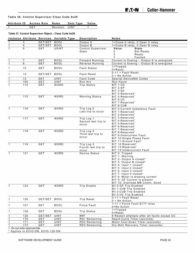
Table 36 . Contro l Supervisor C lass Code 0x29 At t r ibute ID Access Rule Name Data Type Va lue 1 GET Rev is ion U INT 1
Table 37. Control Supervisor Object – Class Code 0x29 Ins tance At t r ibute Services Var iab le Type Descr ip t ion Notes 1 3 GET/SET BOOL Outpu t A 1=C lose A re lay , 0 Open A re lay 1 4 GET/SET BOOL Outpu t B 1=C lose B re lay , 0 Open B re lay 1 6 GET USINT Con t ro l Superv i so r
S ta te Value Sta te 2 No t Ready 3 Ready 7 Fau l ted
1 7 GET BOOL Forward Runn ing Cur ren t i s f l ow ing – Ou tpu t A i s energ ized 1 8 GET BOOL Reverse Runn ing Cur ren t i s f l ow ing – Ou tpu t B i s energ ized
1 10 GET BOOL Fau l t S ta tus 1=Tr ipped 0=Rese t
1 12 GET/SET BOOL Fau l t Rese t 0 ->1 = Fau l t Rese t 0 = No Ac t i on
1 13 GET UINT Fau l t Code Spec ia l Dev iceNet Codes 1 100 GET UINT Run Hrs Run Hours 1 114 GET WORD Tr ip S ta tus
1 115 GET WORD Warn ing S ta tus
B IT 1 :OC B IT 2 :SP B IT 3 :GF B IT 4 :Reserved 1
B IT 5 :Reserved 1
B IT 6 :UC B IT 7 :Reserved 1
B IT 8 :CUB 1 116 GET WORD Tr ip Log 0
Las t t r i p to occur
1 117 GET WORD Tr ip Log 1 Second l as t t r i p to occur
1 118 GET WORD Tr ip Log 2 Th i rd l as t t r i p to occur
1 119 GET WORD Tr ip Log 3 Four th l as t t r i p to occur
B IT 0 :Cur ren t Unba lance Fau l t B IT 1 :Reserved 1
B IT 2 :Reserved 1
B IT 3 :Reserved 1
B IT 4 :Reserved 1
B IT 5 :Reserved 1
B IT 6 :Reserved 1
B IT 7 :Reserved 1
B IT 8 :Reserved 1
B IT 9 :Overcur ren t Fau l t B IT 10 :S ing le Phase Fau l t B IT 11 :Ground Fau l t B IT 12 :Reserved 1
B IT 13 :Reserved 1
B IT 14 :Undercu r ren t Fau l t 1 121 GET WORD Dev ice S ta tus B IT 0 : T r ipped
B IT 1 : Warn ing B IT 2 : Ou tpu t A c losed* B IT 3 : Ou tpu t B c losed* B IT 4 : Inpu t 1 c losed* B IT 5 : Inpu t 2 c losed* B IT 6 : Inpu t 3 c losed* B IT 7 : Inpu t 4 c losed* B IT 8 : Mo to r i s d rawing cur ren t B IT 9 : GF Cur ren t i s p resen t B IT 10 : Over load MB Comm. Good
1 124 GET WORD Tr ip Enab le B i t 0 :GF Tr ip Enab led B i t 1 :VUB Tr ip Enab led B i t 2 :CUB Tr ip Enab led B i t 3 :UC Tr ip Enab led
1 126 GET/SET BOOL Tr ip Rese t 0 ->1 = Fau l t Rese t 0 = No Ac t i on
1 127 SET BOOL Force Fau l t 1 ->1 = Force Fau l t E777 re lay 0=No Ac t ion
1 128 GET BOOL Tr ip S ta tus 1=Tr ipped 0=Rese t
1 130 GET/SET UINT #RF # Res ta r t a t tempts a f te r a l l f au l ts excep t UC 1 170 GET UINT RD1 Remain ing Rap id -Cyc le T imer (seconds) 1 171 GET UINT RD2 Remain ing Moto r Coo l -Down T imer (seconds) 1 172 GET UINT RD3 Remain ing Dry-We l l Recovery T imer (seconds) 1. Do not write reserved bits * App l i es to ECIO-DN, ECIO-120-DN

SOFTWARE DEVELOPMENT GUIDE PAGE 25
Table 37. Control Supervisor Object – Class Code 0x29 Ins tance At t r ibute Services Var iab le Type Descr ip t ion Notes 1 173 GET/SET UINT RD1 Se t t i ng Rap id -Cyc le T imer se t t i ng 1 174 GET/SET UINT RD2 Se t t i ng Moto r Coo l -Down T imer se t t i ng 1 175 GET/SET UINT RD3 Se t t i ng Dry-We l l Recovery T imer se t t i ng 1 176 GET/SET UINT #RU Number o f res ta r t a t tempt a f te r Undercu r ren t fau l t 1 177 GET/SET UINT #RF # Res ta r t a t tempts a f te r a l l f au l ts excep t UC 1 180 GET UINT Power Power i n K i l owa t t s 1 185 GET WORD Tr ip Reason B IT 0 : Lock ou t (a f te r t r i p )
B IT 1 : S top f lag B IT 2 : Con tac t Fa i lu re T r ip B IT 3 : Undercu r ren t T r ip B IT 4 : Overcu r ren t T r ip B IT 5 : Ground fau l t T r ip B IT 6 : Cur ren t Unba lance T r ip B IT 7 : S ing le Phase T r ip
1 186 GET WORD OL S ta tus B IT 0 : Low Vo l tage Pend ing B IT 1 : H igh Vo l tage Pend ing B IT 2 : Vo l tage Unba lance Pend ing B IT 3 : Undercu r ren t Pend ing B IT 4 : Reverse Phase Pend ing B IT 5 : Cur ren t Unba lance Pend ing B IT 6 : Vo l tage S ing le Phase Pend ing B IT 7 : Cur ren t S ing le Phase Pend ing B IT 8 : Overcu r ren t Pend ing B IT 9 : Ground fau l t Pend ing B IT 10 : Reserved 1
B IT 11 : Reserved 1
B IT 12 : Reserved 1
B IT 13 : Reserved 1
B IT 14 : Reserved 1
B IT 15 : Fau l t re lay on 1 190 GET WORD DN S ta tus B IT 0 : Ou tpu t A c losed*
B IT 1 : Ou tpu t B c losed* B IT 2 : E777 Re lay c losed B IT 3 : Reserved 1
B IT 4 : Inpu t 1 c losed* B IT 5 : Inpu t 2 c losed* B IT 6 : Inpu t 3 c losed* B IT 7 : Inpu t 4 c losed* B IT 8 : Reserved 1
B IT 9 : Reserved 1
B IT 10 : Reserved 1
B IT 11 : Reserved 1
B IT 12 : Reserved 1
B IT 13 : Reserved 1
B IT 14 : Reserved 1
B IT 15 : MB. Comm. Loss on E777 1. Do not write reserved bits * Applies to ECIO-DN, ECIO-120-DN
Table 38. Overload Object – Class Code 0x2C Ins tance At t r ibute Services Var iab le Type Descr ip t ion Notes 1 3 GET/SET INT OC Se t t i ng Overcu r ren t T r ip Se t t i ng * A t t r 100 1 4 GET/SET USINT TC Se t t i ng T r ip C lass w i thou t Jam p re f i x 1 5 GET INT Average Cur ren t Average Cur ren t X 10 1 6 GET USINT %CUB % Cur ren t Unba lance (measured) 1 7 GET USINT %Therm. % Therma l Capac i t y Remain ing 1 8 GET INT Cur ren tL1 Phase 1 Cur ren t X 10 1 9 GET INT Cur ren tL2 Phase 2 Cur ren t X 10 1 10 GET INT Cur ren tL3 Phase 3 Cur ren t X 10 1 11 GET INT GF Cur ren t Ground Fau l t Cur ren t X 10 1 100 GET UINT Sca le Fac to r Cur ren t Sca le Fac to r 1 , 10 , o r 100 1 101 GET INT L1 Cur ren t L1 Cur ren t X a t t r i bu te 100 1 102 GET INT L2 Cur ren t L2 Cur ren t X a t t r i bu te 100 1 103 GET INT L3 Cur ren t L3 Cur ren t X a t t r i bu te 100 1 104 GET INT Average Cur ren t Average Cur ren t X a t t r i bu te 100 1 105 GET INT L1 %OC Cur ren t L1 as % o f OC Tr ip Se t t i ng 1. Do not write reserved bits * App l i es to ECIO-DN, ECIO-120-DN

SOFTWARE DEVELOPMENT GUIDE PAGE 26
Table 38. Overload Object – Class Code 0x2C Ins tance At t r ibute Services Var iab le Type Descr ip t ion Notes 1 106 GET INT L2 %OC Cur ren t L2 as % o f OC Tr ip Se t t i ng 1 107 GET INT L3 %OC Cur ren t L3 as % o f OC Tr ip Se t t i ng 1 108 GET INT Avg Cur ren t %OC Average Cur ren t as % o f OC Tr ip Se t t i ng 1 110 GET INT GF Cur ren t Ground Fau l t Cur ren t X a t t r i bu te 100 1 111 GET USINT %Therm %Therma l Capac i t y Rema in ing 1 114 GET INT %CUB % Cur ren t Unba lance (measured) 1 113 GET UINT OL T ime to Rese t T ime remain ing be fo re E777 rese ts 1 114 GET UINT % Cur ren t unba lance % 1 129 GET/SET USINT TC Se t t i ng T r ip C lass w i thou t Jam p re f i x 1 137 GET/SET UINT GF Se t t i ng * ATTR 100 Ground Fau l t T r ip Se t t i ng 1 146 GET/SET UINT UCTD Undercu r ren t T r ip De lay 1 147 GET/SET UINT UC Se t t i ng * ATTR 100 Undercu r ren t T r ip Se t t i ng 1 151 GET/SET UINT CUB L imi t Cur ren t Unba lance Se t t i ng 1 180 GET/SET BYTE Ne tworkWatchdog / Inve r t
Log ic B IT 0 :Enab le Re lay A DN Ne twork Watchdog* B IT 1 :Enab le Re lay B DN Ne twork Watchdog* B IT 2 :Enab le Fau l t Re lay DN Ne twork WatchdogBIT 3 :Reserved 1
B IT 4 : Inve r t Re lay A Log ic * B IT 5 : Inve r t Re lay B Log ic * B IT 6 :Reserved 1
B IT 7 :Reserved 1
1 181 GET/SET BOOL GF Enab le 1=Enab le , 0=D isab le 1 182 GET/SET BOOL TC Jam Enab le 1=Enab le , 0=D isab le 1 183 GET/SET BOOL UC Enab le 1=Enab le , 0=D isab le 1 184 GET/SET BOOL CUB Enab le 1=Enab le , 0=D isab le 1. Do not write reserved bits * Applies to ECIO-DN, ECIO-120-DN
Table 39. Connection Object Class Code 0x77 At t r ibute ID Access Rule Name Data Type Va lue 1 GET Rev is ion U INT 1
Table 40. Voltage Monitor Object – Class Code 0x77 Ins tance At t r ibute Services Var iab le Type Descr ip t ion Notes 1 3 GET UINT Vo l tage Avg Average Vo l tage (measured) 1 4 GET UINT Vo l tage L1 -L2 Vo l tage f rom L1 to L2 1 5 GET UINT Vo l tage L2 -L3 Vo l tage f rom L2 to L3 1 6 GET UINT Vo l tage L3 -L1 Vo l tage f rom L3 to L1 1 7 GET UINT %VUB % Vo l tage Unba lance (measured) 1 8 GET UINT PF Ang le Power Fac to r Ang le 1 20 GET/SET UINT LV Set t i ng Low Vo l tage L imi t 1 21 GET/SET UINT HV Set t i ng H igh Vo l tage L imi t 1 22 GET/SET UINT VUB Se t t i ng %Vo l tage Unba lance L im i t 1 23 GET/SET BOOL VUB Enab le 1=Enab le , 0=D isab le
Table 41. DeviceNet Object – Class Code 0xB4 Ins tance At t r ibute Services Var iab le Type Descr ip t ion Notes 1 7 GET/SET USINT Inpu t Assembly 100 , Word0 1 8 GET/SET USINT Inpu t Assembly 100 , Word1 1 9 GET/SET USINT Inpu t Assembly 100 , Word2 1 10 GET/SET USINT Inpu t Assembly 100 , Word3 1 16 GET/SET USINT Outpu t Assemb ly Ou tpu t Assemb ly Ins tance No .1 17 GET/SET USINT Inpu t Assembly Inpu t Assembly Ins tance No . 1 25 GET/SET USINT Inpu t Assembly 150 , Word0 1 26 GET/SET USINT Inpu t Assembly 150 , Word1 1 27 GET/SET USINT Inpu t Assembly 150 , Word2 1 28 GET/SET USINT Inpu t Assembly 150 , Word3 1 29 GET/SET USINT Inpu t Assembly 150 , Word4 1 30 GET/SET USINT Inpu t Assembly 150 , Word5 1 31 GET/SET USINT Inpu t Assembly 150 , Word6 1 32 GET/SET USINT Inpu t Assembly 150 , Word7 1 33 GET/SET USINT Inpu t Assembly 150 , Word8 1 34 GET/SET USINT Inpu t Assembly 150 , Word9 * App l i es to ECIO-DN, ECIO-120-DN

SOFTWARE DEVELOPMENT GUIDE PAGE 27
Table 41. DeviceNet Object – Class Code 0xB4 Ins tance At t r ibute Services Var iab le Type Descr ip t ion Notes 1 35 GET/SET USINT Inpu t Assembly 150 , Word10 1 36 GET/SET USINT Inpu t Assembly 150 , Word11 1 37 GET/SET USINT Inpu t Assembly 150 , Word12 1 38 GET/SET USINT Inpu t Assembly 150 , Word13 1 39 GET/SET USINT Inpu t Assembly 150 , Word14 1 40 GET/SET USINT Inpu t Assembly 150 , Word15 1 41 GET/SET USINT Inpu t Assembly 150 , Word16 1 42 GET/SET USINT Inpu t Assembly 150 , Word17 1 43 GET/SET USINT Inpu t Assembly 150 , Word18 1 44 GET/SET USINT Inpu t Assembly 150 , Word19 1 45 GET/SET USINT Inpu t Assembly 150 , Word20 1 46 GET/SET USINT Inpu t Assembly 150 , Word21 1 47 GET/SET USINT Inpu t Assembly 150 , Word22 1 48 GET/SET USINT Inpu t Assembly 150 , Word23 1 49 GET/SET USINT Inpu t Assembly 150 , Word24 1 50 GET/SET USINT Inpu t Assembly 150 , Word25 1 51 GET/SET USINT Inpu t Assembly 150 , Word26 1 52 GET/SET USINT Inpu t Assembly 150 , Word27 1 53 GET/SET USINT Inpu t Assembly 150 , Word28 1 54 GET/SET USINT Inpu t Assembly 150 , Word29 1 55 GET/SET USINT Inpu t Assembly 150 , Word30 1 56 GET/SET USINT Inpu t Assembly 150 , Word31 1 57 GET/SET USINT Inpu t Assembly 150 , Word32 1 58 GET/SET USINT Inpu t Assembly 150 , Word33 1 59 GET/SET USINT Inpu t Assembly 150 , Word34 1 60 GET/SET USINT Inpu t Assembly 150 , Word35 1 61 GET/SET USINT Inpu t Assembly 150 , Word36 1 62 GET/SET USINT Inpu t Assembly 150 , Word38 1 63 GET/SET USINT Inpu t Assembly 150 , Word40 1 64 GET/SET USINT Inpu t Assembly 150 , Word41 1 65 GET/SET USINT Inpu t Assembly 150 , Word42 1 66 GET/SET USINT Inpu t Assembly 150 , Word43 1 67 GET/SET USINT Inpu t Assembly 150 , Word44 1 68 GET/SET USINT Inpu t Assembly 150 , Word45 1 69 GET/SET USINT Inpu t Assembly 150 , Word46 1 70 GET/SET USINT Inpu t Assembly 150 , Word47 1 71 GET/SET USINT Inpu t Assembly 150 , Word48 1 72 GET/SET USINT Inpu t Assembly 150 , Word49 1 73 GET/SET USINT Inpu t Assembly 150 , Word50 1 74 GET/SET USINT Inpu t Assembly 150 , Word51 1 127 GET/SET USINT Se t to s tanda lone* Se t th i s to 64 to rese t to an
ECIO s tand-a lone d isc re te I /O modu le
* Applies to ECIO-DN, ECIO-120-DN

SOFTWARE DEVELOPMENT GUIDE PAGE 28
Setup Using EDS Files Each CIO-DN, overload pair must use a DeviceNet EDS file to work with CH Studios or SymCom Solutions software. Each EDS file has an icon associated with it. These EDS and ICO files are available on Cutler-Hammer’s website at www.cutlerhammer.com > USA > Products > Motor Control > Overload Relay > Eaton 777 (E777) Solid-State Overload Relay - DeviceNet EDS. Upload the EDS file to your system to access relevant files. Table 42. EDS file (DeviceNet Communication Module ECOM-DN) up to 480 Volts E777 SSOLR NEMA SIZE AMPERE RANGE EDS FILE NAME ICON FILE NAME E777-LR 00 1-5 (100X) E777_00_v1001.eds E777.ico E777-LR 0 2-9 (100X) E777_0_v1001.eds E777.ico E777 1 5-27(10X) E777_1_v1001.eds E777.ico E777 2 10-45(10X) E777_2_v1001.eds E777.ico E777 3 20-90(10X) E777_3_v1001.eds E777.ico E777-LR 4 60-135(1X) E777_4_v1001.eds E777.ico E777-LR 5 120-270(1X) E777_5_v1001.eds E777.ico E777-LR 6 240-540(1X) E777_6_v1001.eds E777.ico Table 43. EDS file (DeviceNet Communication Module ECOM-DN) up to 600 Volts E777 SSOLR NEMA SIZE AMPERE RANGE EDS FILE NAME ICON FILE NAME E777-575-LR 00 1-5 (100X) E777_575_00_v1001.eds E777.ico E777-575-LR 0 2-9 (100X) E777_575_0_v1001.eds E777.ico E777-575 1 5-27(10X) E777_575_1_v1001.eds E777.ico E777-575 2 10-45(10X) E777_575_2_v1001.eds E777.ico E777-575 3 20-90(10X) E777_575_3_v1001.eds E777.ico E777-575-LR 4 60-135(1X) E777_575_4_v1001.eds E777.ico E777-575-LR 5 120-270(1X) E777_575_5_v1001.eds E777.ico E777-575-LR 6 240-540(1X) E777_575_6_v1001.eds E777.ico Table 44. EDS file (DeviceNet Communication Module ECIO-DN,ECIO-120-DN) up to 480 Volts E777 SSOLR NEMA SIZE AMPERE RANGE EDS FILE NAME ICON FILE NAME E777-LR 00 1-5 (100X) E777IO_00_v1001.eds E777.ico E777-LR 0 2-9 (100X) E777IO_0_v1001.eds E777.ico E777 1 5-27(10X) E777IO_1_v1001.eds E777.ico E777 2 10-45(10X) E777IO_2_v1001.eds E777.ico E777 3 20-90(10X) E777IO_3_v1001.eds E777.ico E777-LR 4 60-135(1X) E777IO_4_v1001.eds E777.ico E777-LR 5 120-270(1X) E777IO_5_v1001.eds E777.ico E777-LR 6 240-540(1X) E777IO_6_v1001.eds E777.ico Table 45. EDS file (DeviceNet Communication Module ECIO-DN,ECIO-120-DN) up to 600 Volts E777 SSOLR NEMA SIZE AMPERE RANGE EDS FILE NAME ICON FILE NAME E777-575-LR 00 1-5 (100X) E777IO_575_00_v1001.eds E777.ico E777-575-LR 0 2-9 (100X) E777IO_575_0_v1001.eds E777.ico E777-575 1 5-27(10X) E777IO_575_1_v1001.eds E777.ico E777-575 2 10-45(10X) E777IO_575_2_v1001.eds E777.ico E777-575 3 20-90(10X) E777IO_575_3_v1001.eds E777.ico E777-575-LR 4 60-135(1X) E777IO_575_4_v1001.eds E777.ico E777-575-LR 5 120-270(1X) E777IO_575_5_v1001.eds E777.ico E777-575-LR 6 240-540(1X) E777IO_575_6_v1001.eds E777.ico

SOFTWARE DEVELOPMENT GUIDE PAGE 29
Configuring Devices using CH Studio Step 1. Start CH Studio Select Tools > Device Manager. CH Studio will bring up the dialog to import EDS files.
Figure 6-EDS Manager Step 2. Click the Import… button to bring up the Import EDS dialog box. Select the EDS files downloaded and click the
import button. CH Studio will list the each file imported and the status of the import.
Figure 8-Import Results
Figure 7-Import EDS

SOFTWARE DEVELOPMENT GUIDE PAGE 30
Step 3. Recovering a faulted node
When a DeviceNet Network is powered up for the first time, all nodes will have the same address. These nodes will go into the faulted state and will appear in CH Studio as Faulted Device. Click on a faulted device. This will cause the faulted to device to identify itself by showing “ICF” on the display or alternate flashing between green and red. (CIO-DN, CIO-120-DN) Click the Recover this device button. This will bring up a dialog box that allows the user to select the address that the faulted node will be set to. Pick the address for the device and click OK
Figure 11-Faulted Node Window
Figure 10-Recovery Window
Figure 9-Recovered Device

SOFTWARE DEVELOPMENT GUIDE PAGE 31
Device Configuration Step 4. Click on a device to view the properties as shown in Figure 12
Figure 12-Device Configuration

SOFTWARE DEVELOPMENT GUIDE PAGE 32
Configuring Variable Input Assemblies Step 1. Enter Parameters to monitor with a poll. In this case parameters 1, 2, 3 are L1, L2, L3 voltages
respectively. These values must match values in the parameter class (see Table 35) Step 2. End the list of parameters with 0. Step 3. Setup input assembly for assembly 100 Step 4. Setup output assembly for desired relay control (see Table 15 through Table 19)
Step 1
Step 2
Step 3
Step 4
Figure 13-Variable Input Assemblies

SOFTWARE DEVELOPMENT GUIDE PAGE 33
Setting the ECIO-DN and ECIO-120-DN to a standalone device Once the ECIO module is plugged into any E777 overload relay, the ECIO’s product code is set to that of the device it is connected to. To set the ECIO module back to a stand-alone device using EDS file Set Parameter 200 to 0x40 To set the ECIO module back to a stand-alone device using CH Studio’s Message Editor. Choose New Message List in the Tasks menu—click Yes. A screen will pop up on the right hand side. Click on the Explicit button in the middle of the screen. Enter the following:
Service: Set Attribute Single (0x10) Class: 0x00B4 Instance: 0x0001 Attribute: 0x7F Data: 40 hex
Click Enter and the message pops up into the message list. Click on it. Then make sure the devices check box is selected (should be in the middle of the screen, just to the left of the message list). Click Send. To verify that it worked, either set up another explicit message or modify the first one, but choose Get Attribute Single and leave the data box empty. Click Send—should get 40 in the Comment box. To set the ECIO module back to a stand-alone device using RSNetworx: You must be connected to the device on the network. Choose Class Instance Editor… in the Device menu—click yes. Enter the following:
Service: Set Attribute Single (0x10) Class: 0x00B4 Instance: 0x0001 Attribute: 0x7F Data: 40 hex
Click Enter. To verify that it worked, either set up another explicit message or modify the first one, but choose Get Attribute Single and leave the data box empty. Click Send—should get 40 in the Comment box. This number being set is the low byte of the product code.

SOFTWARE DEVELOPMENT GUIDE PAGE 34
Using Solutions to configure a DeviceNet scanner Step 1. Start SymCom Solutions Step 2. Select DeviceNet USB/CAN from the Select Network Connection Type dialog box (see Figure 14).
Figure 14-Network Connection Step 3. Select EDS Manager from the Tools menu. Step 4. Click the Import… button in the EDS Manager Window
Figure 15-EDS Manager

SOFTWARE DEVELOPMENT GUIDE PAGE 35
Step 5. Select the EDS files that were downloaded for the E777. Step 6. Click the Open button to import the EDS files. Step 7. Import the EDS file for the scanner that is being configured, by repeating Step 4 through Step 6.
Figure 16-Open Dialog

SOFTWARE DEVELOPMENT GUIDE PAGE 36
Step 8. Once all EDS have been imported, click the Close button on the EDS Manager
Figure 17-EDS Manager

SOFTWARE DEVELOPMENT GUIDE PAGE 37
Step 9. Click Auto Detect Units button in the Navigation Screen Step 10. The first time a DeviceNet network is
commissioned all nodes will be at the same address and appear to a configuration tool as faulted devices. When a device is faulted Solutions will show the dialog see Figure 19.
Figure 19-Faulted Unit Recovery By click Send ICF Request the user can identify the faulted device and assign it an appropriate address. The CIO modules will identify themselves by flashing alternate red and green LEDs. The ECOM-DN attached to an E777 will show ICF on the display of the E777. Step 11. Change the address of the device by
clicking Recover this Device. Step 12. Repeat Step 10 and Step 11 for all faulted
devices. Step 13. Click the scanner icon, and click Download
From Scanner button on the Scanner Settings tab.
Figure 20-Scanner Settings
Figure 18-Network View

SOFTWARE DEVELOPMENT GUIDE PAGE 38
Step 14. Click the Scanlist tab, and select the device to scan from the Available Devices: window Step 15. Click the > button to move the selected device to the Scanlist: window
Figure 21-Scanlist Step 16. Click the device in the Scanlist: window, Verify that the scan parameters are correct for the device; these should
automatically be imported from the device EDS file. Step 17. Click Download Scanlist button to download the Scanlist: windows devices to the scanner.
Figure 22-Scanlist Added
SOFTWARE DEVELOPMENT GUIDE PAGE 39
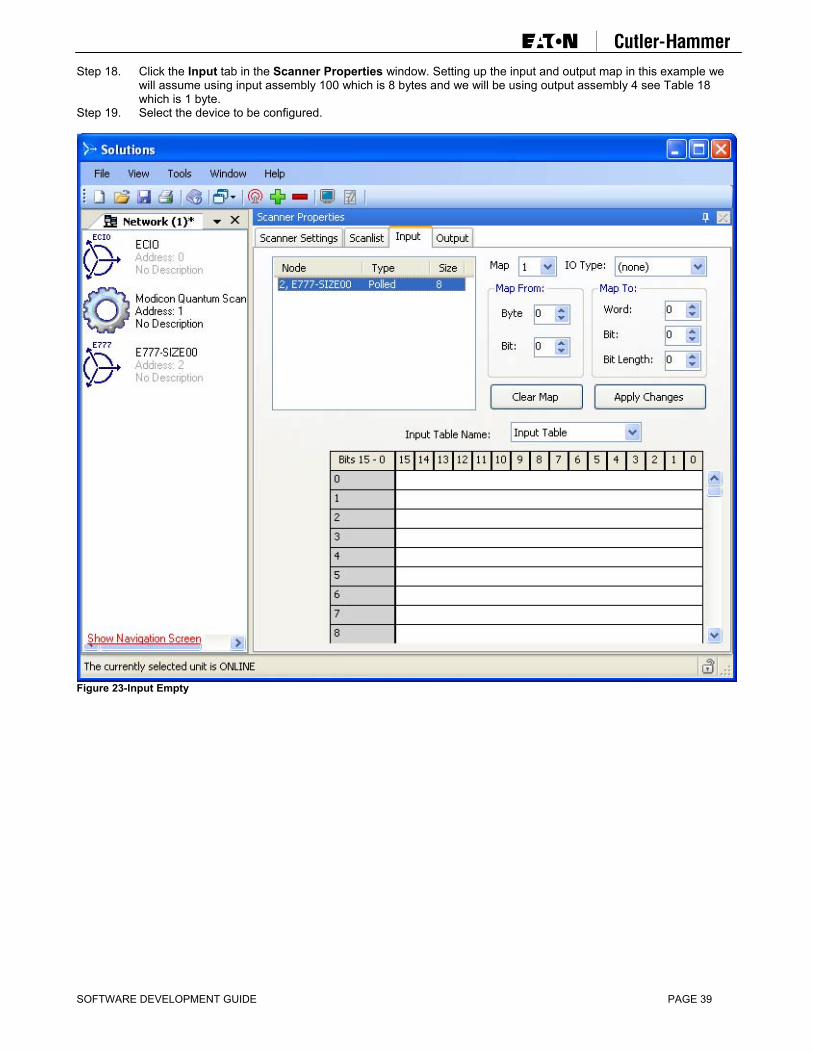
Step 18. Click the Input tab in the Scanner Properties window. Setting up the input and output map in this example we will assume using input assembly 100 which is 8 bytes and we will be using output assembly 4 see Table 18 which is 1 byte.
Step 19. Select the device to be configured.
Figure 23-Input Empty

SOFTWARE DEVELOPMENT GUIDE PAGE 40
Step 20. Select the Map number from the Map drop down box. Solutions allows up to 4 maps Step 21. Select Polled from the IO Type drop down box. Step 22. Select the Byte number in the Byte drop down box in the Map From: panel. For example: using assembly 100
we look at the first word in the parameter view see Figure 13. In this case the first word is 1 which is L1 current * 10 see Table 35. We know that each parameter is 2 bytes longs so when selecting the Byte from the Map From: panel, always use even number to get both the high and low bytes of that parameter.
Step 23. Adjust the Word: drop down box in the Map To: panel, to match the word number where the scanner will store the data coming in from the poll command.
Step 24. Adjust the Bit Length drop down box to 16. All parameter are 2 bytes or 16 bits in length. Step 25. Click the Apply Changes button to commit map changes. Step 26. Repeat Step 20 through Step 25 for all parameter to be mapped. In the case of input assembly 100 the user
could map all 4 parameters; this is shown in Error! Reference source not found..
Figure 24-Input Map

SOFTWARE DEVELOPMENT GUIDE PAGE 41
Step 27. Click the Output tab in the Scanner Properties window. In this example we will be using output assembly 4 which is 1 byte long and controls the A and B relays of the ECIO module.
Step 28. Select the device to be configured.
Figure 25-Output Empty

SOFTWARE DEVELOPMENT GUIDE PAGE 42
Step 29. Select the Map number from the Map drop down box. Solutions allows up to 4 maps Step 30. Select Polled from the IO Type drop down box Step 31. Select the Byte number in the Byte drop down box in the Map From: panel. For example: Using output
assembly 4, this has 2 bits, bits 0 controls relay A , bit 1 controls relay B see Table 18. Step 32. Adjust the Bit: drop down box in the Map From: panel, to matches the bit number for the relay to be controlled. Step 33. Adjust the Word: drop down box in the Map To: panel to 0. Step 34. Adjust the Bit: drop down box to match the bit of the relay to be controlled. Step 35. Adjust the Bit Length drop down box to 1. Step 36. Click the Apply Changes button to commit map changes. Step 37. Repeat Step 29 through Step 36 for all parameter to be mapped. In the case of output assembly 4 there are only
2 relay bits to map as shown in Figure 26.
Figure 26-Output Map

SOFTWARE DEVELOPMENT GUIDE PAGE 43
Step 38. Click the Scanlist tab in the Scanner Properties window. Step 39. Select the target device. Step 40. Click the Upload Scanlist button to commit the mapping changes to the scanner.
Figure 27-Scanlist Upload
![E777 Modbus Master Software Development Guide[1]](https://static.fdocuments.in/doc/165x107/55cf973b550346d0339068cc/e777-modbus-master-software-development-guide1.jpg)