MOBILE AGENT HARDWARE DESIGN FOR DISTRIBUTED WIRELESS NETWORKS
144
MOBILE AGENT HARDWARE DESIGN FOR DISTRIBUTED WIRELESS NETWORKS Sergey Ovcharenko Master of Technology of Electronic Equipment, Kharkov Aviation Institute, 1984 PROJECT SUBMITTED IN PARTIAL FULFILLMENT OF THE REQUIREMENTS FOR THE DEGREE OF MASTER OF ENGINEERING In the School of Engineering Science of School of Applied Science O Sergey Ovcharenko 2006 SIMON FRASER UNIVERSITY Spring 2006 All rights reserved. This work may not be reproduced in whole or in part, by photocopy or other means, without permission of the author.
Transcript of MOBILE AGENT HARDWARE DESIGN FOR DISTRIBUTED WIRELESS NETWORKS

MOBILE AGENT HARDWARE DESIGN FOR DISTRIBUTED WIRELESS NETWORKS
Sergey Ovcharenko Master of Technology of Electronic Equipment, Kharkov Aviation Institute,
1984
PROJECT SUBMITTED IN PARTIAL FULFILLMENT OF THE REQUIREMENTS FOR THE DEGREE OF
MASTER OF ENGINEERING
In the School of Engineering Science
of School of Applied Science
O Sergey Ovcharenko 2006
SIMON FRASER UNIVERSITY
Spring 2006
All rights reserved. This work may not be reproduced in whole or in part, by photocopy
or other means, without permission of the author.

APPROVAL
Name:
Degree:
Title of Project:
Sergey Ovcharenko
Master of Engineering
Mobile Agent Hardware Design for Distributed Wireless Networks
Examining Committee:
Chair: Professor of School of Engineering Science Dr. Ljiljana Trajkovic
Date DefendedIApproved:
Senior ~ u ~ e & i s o r Professor of School of Engineering Science Dr. William A. Gruver
Supervisor
Chief Technology Officer, Intelligent Robotics Corp. Dorian Sabaz

'a' SIMON FRASER W ~ ~ ~ l ~ ~ s d i b r a r y %%&
DECLARATION OF PARTIAL COPYRIGHT LICENCE
The author, whose copyright is declared on the title page of this work, has granted to Simon Fraser University the right to lend this thesis, project or extended essay to users of the Simon Fraser University Library, and to make partial or single copies only for such users or in response to a request from the library of any other university, or other educational institution, on its own behalf or for one of its users.
The author has further granted permission to Simon Fraser University to keep or make a digital copy for use in its circulating collection, and, without changing the content, to translate the thesislproject or extended essays, if technically possible, to any medium or format for the purpose of preservation of the digital work.
The author has further agreed that permission for multiple copying of this work for scholarly purposes may be granted by either the author or the Dean of Graduate Studies.
It is understood that copying or publication of this work for financial gain shall not be allowed without the author's written permission.
Permission for public performance, or limited permission for private scholarly use, of any multimedia materials forming part of this work, may have been granted by the author. This information may be found on the separately catalogued multimedia material and in the signed Partial Copyright Licence.
The original Partial Copyright Licence attesting to these terms, and signed by this author, may be found in the original bound copy of this work, retained in the Simon Fraser University Archive.
Simon Fraser University Library Burnaby, BC, Canada

ABSTRACT
For more than a century, the communications systems have been evolving
towards hierarchical networking architectures. The central problem in such networks is
that the communications domain is a separate entity to the applications domain. With the
advent of powerful and small microcontrollers and cheap memory, it is now feasible to
start merging these two domains into one Holonic domain, where all contributing nodes
participate together providing both roles of communication and application functionality.
A flatter network infrastructure becomes possible, and the entire system of nodes can be
viewed as a distributed intelligent system.
This report is based upon the examination and design of an electronic device
enabling the development of distributed intelligent systems. Specifically focusing on the
key hardware requirements for constructing a small modular package for communication,
data processing, and memory support for a wireless distributed intelligent system.
Keywords: holonic, distributed intelligent systems, peer-to-peer

DEDICATION
To my parents, Victor and Anellya Ovcharenko for the inculcated love of
knowledge and vigorous support in education and every aspect of life.

ACKNOWLEDGEMENTS
My special words of gratefulness are addressed to Dr. William A. Gruver,
professor of School of Engineering Science at Simon Fraser University, and Dorian
Sabaz, Chief Technology Officer at Intelligent Robotic Corporation, for their guidance in
both academic and industrial spheres during my work on the project presented in this
report. Under their supervision, I gained competence in the exciting subject of Holonic
Mobile Networks that helped me successfully cope with all challenges throughout this
work.

TABLE OF CONTENTS
. . .......................................................................................................................... Approval 1 1
... Abstract ........................................................................................................................ 111
Dedication ......................................................................................................................... iv
Acknowledgements ............................................................................................................ v
............................................................................................................. Table of Contents vi ...
List of Figures ................................................................................................................ VIII
...................................................................................................................... List of Tables x
............................................................................................................................ Glossary xi
1 Introduction ................................................................................................................ 1 ................................................................ 1.1 Conventional Communication Systems 2
1.2 Distributed Systems vs . Centralized Systems ....................................................... 3 1.2.1 Degrees of Distribution .................................................................................. 4 1.2.2 Existing Decentralised Systems ..................................................................... 9
....................................................................... 1.3 Holonic Communication Systems 14 1.3.1 Holonic Systems ........................................................................................... 14
............ 1.3.2 Holonic Systems as An Alternative to Traditional Communication 15 1.4 Scope of the Design ............................................................................................. 17
1.4.1 Objectives and Goals .................................................................................... 18 1.4.2 Design Requirements ................................................................................... 19
2 Engineering Analysis ................................................................................................ 20 ............................................................................................ 2.1 Project Initialization 20
................................................................... 2.2 System Architecture Considerations 20 ................................................................................. 2.2.1 System Requirements 1
. . ..................................................................... 2.2.2 Components Selection Cnter~a 22 .......................................................................... 2.3 Existing Memory Technologies 22
..................................................................... 2.3.1 Non-volatile Memory Devices 23 2.3.2 Volatile Memory Devices ............................................................................ 40 2.3.3 Comparative Analysis of SRAM and DRAM Devices ................................ 43
2.4 CPU Selection ..................................................................................................... 45 ........................................................................... 2.4.1 Prototype I CPU Solutions 45
..................................................................... 2.5 Components for Wireless Interface 51 ................................................ 2.5.1 Fundamentals of 802.1 1 Wireless Networks 51
2.5.2 Multipath Loss .............................................................................................. 58 .......................................................................... 2.5.3 Wireless Platform Analysis 60
............................................................................................. 3 HCS Hardware design 63 3.1 Functional Design ................................................................................................ 63 3.2 Memory Selection ............................................................................................... 64
.................................................................................................... 3.2.1 NOR Flash 65 3.2.2 NAND Flash ................................................................................................. 65
........................................................................................................ 3.2.3 SDRAM 65 .................................................................................. 3.3 Detailed Hardware Design 65
............................................................. 3.3.1 Architecture of the HCS Controller 65 ........................................................... 3.3.2 Architecture of the HCS Transceiver 67
................................................................ 3.4 Electrical Circuit Design and Analysis 69 .............................................................. 3.4.1 Characteristics of Micro-controller 69
........................................................................................ 3.4.2 Design Challenges 70 3.4.3 Design Solutions .......................................................................................... 71 3.4.4 Power Distribution ....................................................................................... 77
..................................................................................... 3.4.5 PCB Considerations 78 ......................... 3.5 Comparative Analysis of Prototype I and Prototype 11 Designs 91
.................................................................. 4 Manufacturing. testing. quality control 92 ................................................................................... 4.1 Design for Manufacturing 92
..................................................................... 4.1.1 PCB Manufacturing Strategies 92 . .
4.2 Quality Control Criteria ....................................................................................... 93 ............................................................................................... 4.3 Design for Testing 93
....................................................................................................... 4.4 Cost Analysis 93
5 Conclusions ............................................................................................................... 96 ...................................................................................................... 5.1 Achievements 96
.............................................................................................. 5.2 Design Prospective 96
Appendices ........................................................................................................................ 99 ......................................... Appendix A: Schematic Diagrams of the HCS Controller 100
Appendix B: Manufacturing Files (Gerbers) of the HCS Controller .......................... 109 Appendix C: Schematic Diagram of the HCS Transceiver ......................................... 124 Appendix D: Manufacturing Files (Gerbers) of the HCS Transceiver ....................... 126
................................................................................................................. Reference List 131

LIST OF FIGURES
Figure 1.1 . Architecture of a contemporary communication network .............................. 2
Figure 1-2 . Centralized, ring, and hierarchical network topologies .................................. 7 Figure 1-3 . Examples of hybrid network topologies ........................................................ 8
Figure 1-4 . Hybrid P2P architecture ............................................................................... 10
Figure 1-5 . Steps required to establish data transfer in a purely decentralized P2P network .............................................................................................. 1
Figure 1-6 . An example of a mesh network configuration ............................................. 13
Figure 1-7 . Relation between domains in traditional communication systems .............. 16
Figure 1-8 . Merging communication and application domains in a holonic network ......................................................................................................... 17
Figure 1-9 . Architecture of the Holonic Technology Platform (HTP) ........................... 18 Figure 2- 1 . Typical floating gate MOSFET memory cell ............................................... 24
Figure 2-2 . Architecture of NOR flash memory ............................................................. 27 Figure 2-3 . Erase and programming methods of the flash cell ....................................... 29
Figure 2-4 . Architecture of NAND flash memory .......................................................... 33 Figure 2-5 . Organization of a small block 1GBit NAND flash ...................................... 34
Figure 2.6 . Organization of a large block 1Gbit NAND flash ........................................ 35 Figure 2-7 . SRAM cells: a) typical 4T2R cell, b) 6T-cell .............................................. 41
Figure 2-8 . DRAM cell: a) Schematic representation, b) Planar cross-section .............. 42 Figure 2-9 . Architecture of independent basic service set (IBSS) .................................. 52 Figure 2-1 0 . Architecture of basic service set (BSS) network type .................................. 53 Figure 2-1 1 . Architecture of extended service set (ESS) wireless LAN ........................... 54 Figure 2- 12 . An example of a frequency hopping pattern ................................................ 55 Figure 2- 13 . Three non-overlapping channels of the DSSS 802.1 1 WLAN .................... 57
Figure 2- 14 . Multipath signal propagation ....................................................................... 59 Figure 3-1 . Architecture of the holonic mobile agent ..................................................... 63 Figure 3-2 . Architecture of the holonic mobile agent controller .................................... 67
Figure 3-3 . Architecture of the holonic mobile agent transceiver .................................. 68 Figure 3-4 . Blocks of the PXA270 processor essential for HCS controller design ........ 69 Figure 3-5 . SDRAM array organization ......................................................................... 72 Figure 3.6 . NOR flash array organization ...................................................................... 73 Figure 3-7 . NAND flash array organization ................................................................... 74
Figure 3-8 . Power distribution of the HCS controller ..................................................... 77

Figure 3.9 . HCS controller 8-layer board layer stack-up ................................................ 80 Figure 3.10 . Escape routing for the PXA270 (a) and NOR Flash (b) on the top
layer ......................................................................................................... 1 Figure 3-1 1 . Memory components placement on the board ............................................. 87
Figure 3.12 . 3D model of the top side of the controller board ......................................... 88
Figure 3.13 . 3D model of the bottom side of the controller board ................................... 89
Figure 3.14 . HCS transceiver 2-layer board layer stack-up .............................................. 90

LIST OF TABLES
Table 2.1 : Table 2.2 Table 2.3:
Table 2.4: Table 2.5: Table 2.6: Table 2.7: Table 2.8:
Table 2.9:
Table 2.10: Table 2.1 1 : Table 2.12: Table 3.1 : Table 3.2:
Table 3.3: Table 3.4: Table 4.1 : Table 4.2: Table 4.3:
Commercially available NOR flash devices ................................................ 32 Small-block vs . large-block NAND flash performance ............................... 35 Small-block NAND flash devices ................................................................ 36 Large-block NAND flash devices ................................................................ 36
Commercially available ML flash devices ................................................... 38 Serial EEPROMIFLASH devices ................................................................. 39
Random access memory devices .................................................................. 44 Comparative characteristics of the StrongArm family processors ............... 46 Comparative characteristics of some commercially available processors for mobile applications ............................................................... 49 Symbol to frequency mapping in 4 GPSK ................................................... 56 Chip to differential phase mapping in 4 DQPSK ......................................... 57 Commercially available system-in-package 802.1 1 Solutions .................... 62
....................................................................... HCS controller memory map 75 Summary of currently available PCB features ............................................. 78
Design rules for the holonic controller PCB ................................................ 81 Comparative characteristics of Prototype #1 and Prototype #2 ................... 91
Summary of the controller prototypes building costs .................................. 94 Summary of the transceiver prototypes building costs ................................ 94 Total best and worst costs per prototype unit ............................................... 95

GLOSSARY
AP - BGA - BPSK - BSS - CCITT - CHEI - CS - DRAM - DS - DSL - DSSS - ENIG - ESS - FG - FHSS -
FNT -
GFSK - GPIO - HASL - HCS - HIS - HLS - HSS - IBSS -
IC - ISDN - ITU - LSB - MSB - PCB - SDRAM Sip -
SMD - SMT - SRAM -
Access Point Ball Grid Array Binary Phase Shift Keying Basic Service Set International Telephone and Telegraph Consultative Committee (see ITU) Channel Hot-Electron Injection Chip Select Dynamic Random Access Memory Distribution System Digital Subscriber Line Direct Sequence Spread Spectrum Electroplated Nickel / Immersion Gold Extended Service Set Floating Gate Frequency Hopping Spread Spectrum Fowler-Nordheim Tunnelling Gaussian Frequency Shift Keying General Purpose Input/Output Hot Air Solder Level Holonic Communication System Holonic Intelligence System Holonic Logistic System Holonic Strategic System Integrated Basic Service Set Integrated Circuit Integrated Services '~i~ita1 Network International Telecommunications Union, formerly CCITT Least Significant Bit Most Significant Bit Printed Circuit Board - Synchronous DRAM System-in-Package Surface Mount Design Surface Mount Technology Static Random Access Memory

1 INTRODUCTION
The past century may be recognised as the fastest period of technical progress in
many areas of human life. However, without any doubt it can be called an era of
achievements in communications. During this period, communication systems progressed
from the very simple methods of information exchange to sophisticated techniques,
devices, and equipment. The following is a list of some important dates from the history
of communication systems development.
1876 - telephone invented
1895 - first radio signal sent and received
19 14 - first cross-continental telephone call made
1926 - first radio network, NBC, is formed
1957 - first satellite launched and first case of satellite communication established
1979 - first commercial cellular telephone system deployed in Tokyo
1982 - introduction of TCPIIP by DoD as a standard
1984 - initial deployment of Advanced Mobile Phone Service (AMPS) cellular
system
1984 - introduction of ISDN in CCITT Recommendation I. 120
1989 - DSL designed
199 1 - World-Wide Web (WWW) is released
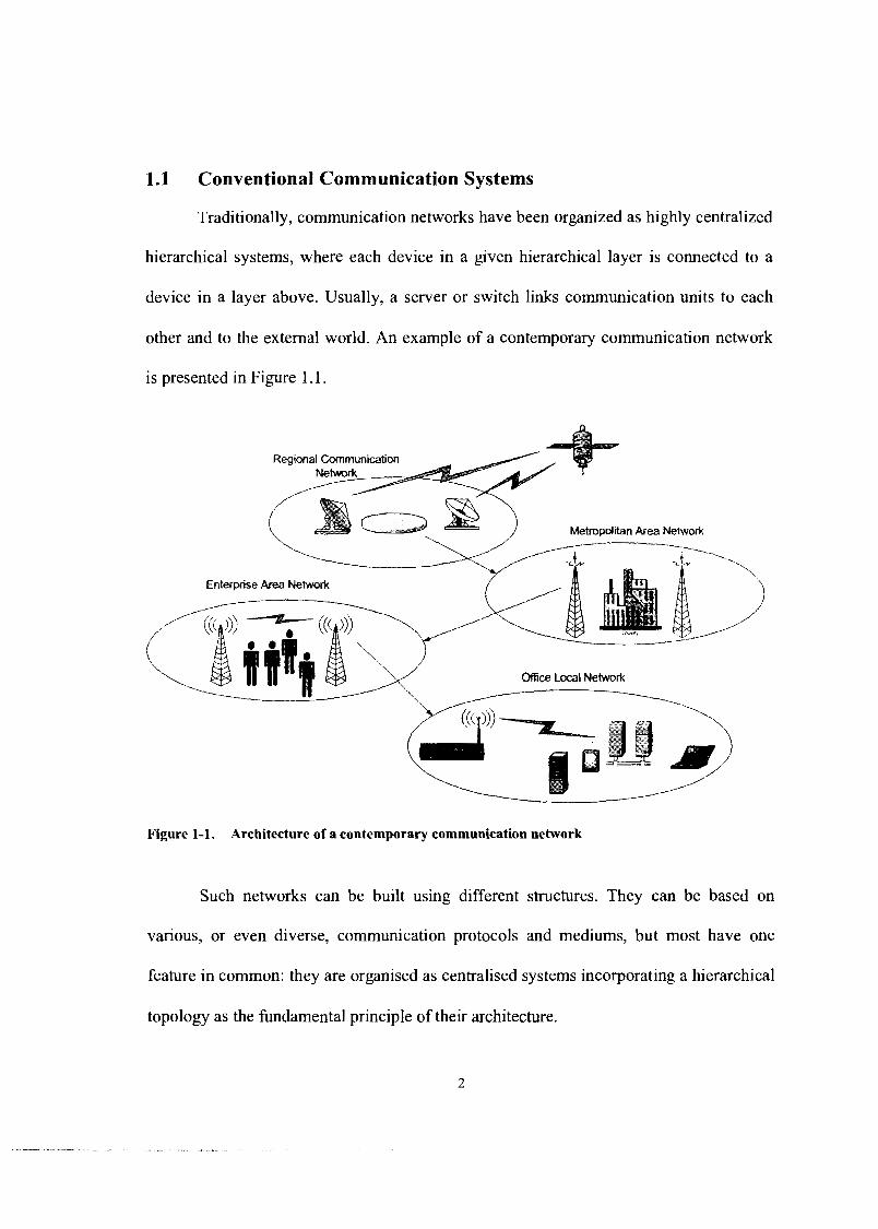
1.1 Conventional Communication Systems
Traditionally, communication networks have been organized as highly centralized
hierarchical systems, where each device in a given hierarchical layer is connected to a
device in a layer above. Usually, a server or switch links communication units to each
other and to the external world. An example of a contemporary communication network
is presented in Figure 1.1.
Regional Communication
(i/B Metropditan Area Network
Figure 1-1. Architecture of a contemporary communication network
Such networks can be built using different structures. They can be based on
various, or even diverse, communication protocols and mediums, but most have one
feature in common: they are organised as centralised systems incorporating a hierarchical
topology as the fundamental principle of their architecture.

Having been developed for significant time, these systems achieved high
efficiency and have a set of numerous advantages, including:
Good control from top to bottom;
Easily provided security;
High manageability;
Potential for scalability.
However, all these benefits of centralised systems decline with growing
hierarchy:
Resources are not easily available for all participants of the network;
Intelligence is removed from the communication domain;
Control at the top of hierarchy is separated from knowledge at the bottom;
Effectiveness drops and maintenance costs grow.
1.2 Distributed Systems vs. Centralized Systems
As an alternative to widely spread centralised networks, decentra
have been introduced and developed. They are intended to directly
d systems
connect
communicating devices and make their communication more effective. However, most of
such systems implement only some degree of decentralisation and require proper analysis
before classifying them as decentralised or distributed. Some strategies of approach to
analysing a network in terms of distribution are described in the following section.

1.2.1 Degrees of Distribution
Relative centralization or decentralization of the system elements can be
described by degrees of distribution. A collection of system resources may be distributed
in terms of the following characteristics:
Location: physical distances among the elements of a network. It results in
o highly efficient and cost-effective utilization of resources,
o investment concentrated in a single location and resources not duplicated
elsewhere in the system,
o relative ease of enforcing policies and procedures uniformly,
o removing information processing functions from sources of transactions
and the locations of user groups.
Function: position of an activity or responsibility within the structure of a network.
Centralization of function is particularly ineffective if
o different functions are highly interdependent,
o close working contact is required among the functions,
o required to respond to exceptional or unique situations.
Control: disperses responsibilities among different levels of the system.
o applies and enforces policies consistently and uniformly,
o problems solving is removed from their immediate circumstances.
o delays or failures in communication can result in inappropriate decisions.

1.2.1.1 Network configurations
Different network configurations represent different degrees of distribution
required to balance efficiency with effectiveness. Options available to the system
designer include
Centralized processing with remote access
Distributed processing with centralized control
Semi-autonomous distribution of processes
Satellite processing
Standalone facilities with shared resources
Load sharing.
Centralized processing with remote access.
In this structure, network elements serve as terminals that share access to the central host.
This type of network is distributed with respect to input and output hnctions. Processing
and data storage functions are centralized. Terminals submit data to the host, and, under
control of the host, provide outputs. (e.g., ATM machines at banks.)
Distributed processing with centralized control. A supermarket checkout
system is an example of distributed processing with centralized control. In this
configuration, entire processing cycles are performed at the store level. That is, normal
store operation does not depend on intervention from the central computer. However,
control is retained centrally, since the corporate computer could cause either program or
data in the store computers to be updated during any polling cycle.

Semi-autonomous distribution of processing. In this network, the local
computers each act as hosts within their own respective networks of distributed terminals.
Most processing cycles are performed completely at the regional level. The central
computer in this case does not control the processing cycles of the regional systems.
Rather, it collects summaries from the regions periodically.
Satellite processing. Under this approach, the central computer is, in effect,
eliminated and all processors within the network have roughly equal status. That is, none
of the units can be identified as a controller to which others might respond. Thus, a
satellite configuration typically reflects a high degree of regional or divisional autonomy
with minimal central control.
Standalone facilities with shared resources. An example of such a system is a
local area network (LAN) that supports independent operations of numerous units. Each
unit is capable of controlling complete processing cycles without the aid of others.
However, for the reasons of economy, or the need of information sharing, some elements
within the network are shared.
Load sharing. Within such networks, each node is a semi-autonomous processor
capable of executing any task that is presented to the system. Particularly in high volume
applications and during peak periods, contention, or conflicting access demands, might
cause one of the processors to become swamped. [ l ]

1.2.1.2 Network Topologies
To distinguish a centralized system from decentralized system it is appropriate to
consider them in terms of topology. Most of the contemporary communication networks
can be classified according to their topologies as follows.
The most popular and well-known is the centralized type of topology. This system
is utilized by various databases, clientlserver systems and web servers. This type of
systems is depicted in the Figure 1.2.a and characterized by good manageability,
information coherence and security located at a single host. On the other hand, they have
low-level fault tolerance and resistance to external intervention.
a) Centralized
Figure 1-2. Centralized, ring, and
0 0' '
I
b) Ring c) Hierarchical
hi ~erarchical network topologies
The ring systems are built for the communicating devices located nearby. It is
typical for such systems to have high-level manageability, information coherence, fault
tolerance and security. However, these systems are not easily extensible and are easy to
shut down. It can be seen in the Figure 1.2.b.
In the hierarchical systems, information exchange is realized along tree-like paths,
as shown in the Figure 1 . 2 ~ . As a result, they have good scalability combined with

moderate manageability, information coherence, extensibility and fault tolerance,
however, they have low-level security.
Decentralized systems are based on the topology shown in Figure 1.3a. The
devices in such a structure have equal roles and communicate symmetrically. The
advantages of decentralized systems are extensibility, fault tolerance and resistance to
intervention. As weaknesses, they have low manageability, information coherence and
security.
There is also a variety of hybrid topologies available for communication
networks, two examples of which are shown in Figures 1.3b and 1 . 3 ~ .
a) Decentralized b) Centralized + Ring c) Centralized + Decentralized
Figure 1-3. Examples of hybrid network topologies
These systems are recognized for their moderation of advantages pertaining to a
pure topology as a cost for the mitigation of weaknesses due to the merging of two or
more types.

1.2.2 Existing Decentralised Systems
A number of attempts have been made to compromise on shortcomings of
centralised systems. Below, there are some examples of the solutions offered in creating
decentralised networks.
1.2.2.1 Peer-to-Peer Systems
A peer-to-peer (P2P) network is a network in which clients communicate and
share information via large number of ad hoc connections rather than relying on the
network severs. In such a network equal peers act as clients and servers simultaneously.
Numerous P2P networks have been introduced and widely used for data, audio and video
exchange. Such networks as Napster, Kazaa, Gnutella and others use P2P principles for
all purposes or as an extension to a clientlserver structure. Existing architectures can be
classified as [2]:
Hybrid,
Partially Centralized,
Purely Decentralised.
In the Hybrid architecture, a computer that wants to join the network informs the
server about the contents it has. A client sends a request to server, and the server looks
for machines carrying the requested file. After such an owner has been found, a direct
connection between the requester and the file owners is established and data exchange
starts. An example of a Hybrid peer-to-peer architecture can be seen in the Figure 1.4.

Figure 1-4. Hybrid P2P architeicture
Advantages of Hybrid decentralised systems are:
- Simple to implement,
- Quick and efficient in locating data.
The main weakness are susceptibility to censorship, malice attack and technical
failure due to access control maintained by a single entity. For the same reason, these
systems are non-scaIable.
In a Purely Decentralised System., its members do not rely on the information
stored at a single server location, but send broadcast query messages to all neighbours.
Once a response from a node: owning a requested file has been received though the path

along which the request propagated, a. direct connection is established and downloading
begins. An example of request propagation and reply is presented in Figure. 1.5.
/-----,, ( Client r L--_1_1---1
Figure 1-5. Steps required to establish data transfer in a purely decentralized P2P network
Partially Centralised Systems are sfmilair to Purely Centralised and differ from the
former in having super node:^". These s~lpernodes are dynamically selected from the
other network nodes as devices with suffic:ient bandwidth and processing power and are
responsible for servicing a small subpart of the peer network.
As it is has been shown, the P2P so'lution for distribution is realised mlostly on the
application level and does not change physical routing of the information streams.

1.2.2.2 Mesh Networks
A Mesh network is an approach to create a distributed system for routing data,
voice and commands between nodes by employment of hopping from node to node until
continuous communication established. These systems are recognised for their self-
healing, meaning that if a node is broken the communication path can be re-established
via other nodes. Mesh networks especially benefit from implementation of wireless
methods of communication and find application in providing Internet service for houses
and buildings in same neighbourhood, security and surveillance information exchange,
military solutions, etc. An example of a Mesh network configuration and application can
be seen in Figure 1.6.
Networks of this type have been developed by Microsoft, Motorola, Nortel, and
other companies. Among the advantages of mesh networks are
Sharing access to a higher cost infrastructure;
Dynamic routing capabilities;
Applicability to mobile devices;
High reliability.

Figure 1-6. An example of a mesh network configuration
Even though the networks described above and others similar to them are
frequently presented as distributed, they remain centralised from the topological point of
view because they rely on the existing physical network components. The only way to
build a purely distributed system is to abandon approaches and system elements and
realize a new design, an example of which is a Holonic network described in the next
section.

1.3 Holonic Communication Systems
1.3.1 Holonic Systems
Holonic systems are based on highly decentralized communication networks built
from a modular mix of semi-standardized, autonomous, cooperative, and intelligent
elements, called "holons".
The term "holon" was introduced by Arthur Koestler as a combination of the
Greek word "holos" meaning "whole" and the suffix "on", which is present in such
words as proton or electron to portray a particle or part. Thus, holon stands for an entity
that has a dual nature of being seen as a whole for subordinated elements and as a part
when viewed from a higher level of hierarchy.
The physical holons consist of equipment responsible for fulfilment of assigned
tasks and of holonic control devices, providing inter-holon communication, real-time
control, and physical interfaces between processing equipment.
A holonic system targets the following performance features:
Holonic Control Devices (HCD) must be implemented as interoperable and
heterogeneous units organized as a distributed control system;
HCDs must be rapidly automatically reconfigurable by software agents due
to the rapidly reconfigurable physical equipment;
HCDs must provide adequate user interfaces at all functional levels.
These goals can be achieved by fulfilling two basic requirements:
High degree of software encapsulation, portability, and reusability;

Independence of platform and communication layer from the control
applications combined with dynamic self-reorganization
A key component of a holonic communication system is spontaneous networking
that is characterised by the following features and described by Coulouris et a1 in [3]:
Easy connection to a network: A device should be transparently reconfigured
to obtain connectivity when brought into the network.
Easy integration with services: Devices automatically discover what services
are provided by the network.
Limited connectivity: System must respond to the situation when devices
appear and disappear from the network as they travel due to the nature of
mobility.
Security and privacy: While supporting continuously changing number of
mobile agents, the system should provide an adequate level of security
distinguishing eligible participants from intruders.
1.3.2 Holonic Systems as An Alternative to Traditional Communication
If we look at the Holonic network as an alternative to existing communication
structures, it is possible to summarise their features as described below and in Figures
1.7. and 1.8.
Traditional Systems:
Intelligence distributed only at the fringes of the communications network
High network utilization; services are remote requiring large number of hops

c tructure High reliance on single network iinfra,;
- Communications infrastructure only links intelligent systems.
Figure 1-7. Relation between domains in traditionall communication systems.
Holonic Systems:
Applications and Communications Domains are merged to a Holonic Domain
Lower network utilization; services are local to users
Network communication has high, redundancy
Communications infrastructure proviaks an intelligent system.

Figure 1-8. Merging communica~tion and application domains in a holonic network
1.4 Scope of the Design
In order to implement a wireless network system based on a holonic architecture,
the Holonic Technology Platform relies on two major components - Holonic
Communication System (HCS) hardwar'e and Holonic Intelligence System (HIS)
software. The HIS is composed of two sub--systems: Holonic Logistic System (HLS) and
Holonic Strategic System (HSS). The former is responsible for monitoring the
administration functionality of each holon, collecting and managing the resources that are
available throughout the network, and the communication functionality. The latter
coordinates and plans activities between the holons spread over the network [4:1. The HTP
architecture is depicted in Figure 1.9.
To perform strategic analysis, the HSS requests a list of the resources acquired by
each node of the network. The HLS fetches this information from the nodes located
within a specified number of hops. Once the analysis has been completed by the HSS, the
HLS can allocate resources and transfer data. One of the tools the HLS uses to carry out

these duties is based on keeping track of the different network topologies available to the
holon, including Virtual Networks (VN). It is important to provide that several VNs can
be accessed simultaneously.
Figure 1-9. Architecture of the IIolonic Technology .Platform (HTP)
1.4.1 Objectives and Goals
To develop a highly decentralized communication network based on principles of
holonic devices, the objective of this project is to design and build a physical prototype
demonstrating feasibility of this approach and supporting further research in this
direction. The highest level of distribution is to be combined with unconstrained mobility.
Wireless communication provides the best choice to satisfy these requirements.

1.4.2 Design Requirements
As shown above, since mobile holonic devices contain both an information part
and a physical part, and are essentially adaptive agent-machine systems, they are
intended to transmitlreceive, process and store significant volumes of information. This
raises a special set of requirements for the hardware portion of the design:
High volumes of information exchanged between the holons require
a) significant space for data storage;
b) high speed communication channels;
c) high speed data processing.
Mobile devices are to be compact to meet constraints for various
applications.
Hardware design must provide flexibility to change the communication
protocol/medium, if necessary.
Taking into account that the prototype is intended for extended software development it
may have additional features and capabilities to support expected as well as unexpected
needs imposed by all levels of software.
In addition, since this device is being introduced as a second generation in the family of
the holonic hardware prototypes [5] , it should provide maximum compatibility for the
low-level software previously created for the first prototype.
2 ENGINEERING ANALYSIS
2.1 Project Initialization
This project represents a second step in Holonic Mobile Agent development.
Previous work has been done to create a start-up platform for building an information
layer of a Holon-based mobile network. This work, described by Wong in [5], realized a
hardware prototype designed around an Intel PXA255 core processor. At a certain
development stage, this device, even though efficient at the earlier design phases and
comprising 128 Mbits of SDRAM and 128 Mbits of NOR flash, had required further
modifications to satisfy the growing needs of the software.
Thus, to provide an effective physical part for the holonic mobile agent a device
of a higher performance level is to be built. At this stage, the design is expected to:
- provide communication via a real wireless medium;
- support a high-speed communication interface to a host device;
- provide sufficient storage for embedded software and data;
- be built using modern technologies and advanced components base;
- provide an effective platform for further integration and micro-miniaturization
2.2 System Architecture Considerations
This chapter provides architectural design considerations that are necessary for
the components selection and effective utilisation of the system resources.

2.2.1 System Requirements
Analysis of previous results helped to create a list of the system requirements for
the prototype that I developed. These requirements are as follows:
Architecture
The mobile device is to be built of two entities - a Controller responsible for
intelligent networking and data processing, and a Wireless Transceiver providing
communication interface with other mobile agents.
Memory
at least 1 GByte space for embedded programs,
1 GByte of non-volatile data storage,
1 GByte of high-speed random access memory for programs and data.
Central Processor Unit (CPU)
run at frequencies 400 MHz and higher,
provide on-chip CASH memory for frequently accessed data,
support various communication interfaces,
be available in compact packages.
Communication Medium
The device should communicate with other mobile devices via a wireless (WiFi)
interface
Periphery should be available in the form of commonly used interfaces, such as:

USB,
SPI,
PCMCIA.
2.2.2 Components Selection Criteria
For further architectural design, all components required for the devices can be
arranged into several major groups:
Memory devices
a) Non-volatile memory,
b) Random Access Memory (RAM),
CPU
Wireless communication components,
Discreet semiconductors and low-integration Integrated Circuits (ICs).
To assist with components selection for each group required for the design a
review of the existing technologies and modern devices for mobile communication is
provided in the following subsections.
2.3 Existing Memory Technologies
To provide sufficient space for potentially vast arrays of data and, at the same
time, have large residence for the application programmes it is appropriate to utilize two
types of non-volatile memory - NAND flash and NOR flash. Additionally, the device

needs the equivalent area of memory to unpack the software saved in flash upon booting
and to store temporary products of data processing.
2.3.1 Non-volatile Memory Devices
Non-volatile memories are essential part of any intelligent electronic system that
is characterised by the capability to store information in the absence of power. In the past,
various types of non-volatile memory have been available, including Read-only
Memories (ROM), Programmable ROM (PROM), Erasable PROM (EPROM), and Ultra-
Violet EPROM (UV - EPROM). Electrically Erasable PROM had a wide range of
applications because along with fast random read and write access to any location it
offered the advantage of in-circuit programming and erasing. First-generation EEPROM
devices had parallel interface, which at higher densities leads to large package sizes. In
addition, EEPROM architecture is based on a two-transistor cell that consists of a large
write transistor and a small read transistor that results in a significant area required for
large memory arrays.
2.3.1.1 Flash Memory Architectures
Flash memory is a variant of EEPROM that is developed in two main directions:
traditional random access type and byte serial memories. All flash memories are similar
in employing sectored memory arrays. Depending on the Flash memory type, sectors -
also referred as blocks - can be equal in size or consist of different number of cells.
The major difference of a flash memory cell from EEPROM is the absence of the
select transistor in order to achieve higher density and cost saving. This feature brings the
concern of possible interference with one portion of the memory while writing to another

portion, thereby requiring tighter control of the process parameters for manufacturing [6] .
A cross-section of the standard flash memory cell (T-cell) is based on the floating gate
MOSFET and shown in Figure 2.1.
Control Gate
lnterpoly Dielectric 15 ... 30 nrn I Floating Gate
r / Gate Oxide O-I 8...12 nm
Figure 2-1. Typical floating gate MOSFET memory cell
In a Floating Gate (FG) memory device, the floating gate is entirely surrounded
by a dielectric that prevents electrons from travelling to and from the FG. The principle
of its operation is based on Channel Hot-Electron Injection (CHEI) programming and
Fowler-Nordheim (FN) Tunnelling for erasing. FN Tunnelling takes place in the presence
of a strong electrical field that allows electrons to pass from the conduction band of one
silicon region to the conduction band of another silicon region through an intervening
barrier of SO2. The cell is programmed using Channel Hot-Electron Injection that occurs
when the cames are accelerated to a sufficiently high energy level to pass through the
bamer. If a high voltage is applied to the source and the control gate is grounded, a high
electric field induced in the oxide, forcing electrons to flow from the floating gate to the

source. This bias condition is very close to the source-substrate breakdown level. To
reduce the breakdown voltage the source region usually consists of an nf diffusion region
inside of an n-type diffusion. The drain region consists of nf source/diffusion that
underlies the floating gate. A uniform gate oxide, from 8 to 12 nm thick, lies between the
FG and the p-substrate. The control gate, made of polysilicon or polycide, is isolated
from the floating gate with a dielectric 15 to 30 nm thick.
During the write operation, a high positive voltage of 12V is applied to the control
gate. An inversion region is formed in the p-substrate. The source is connected to the
ground and the drain level is half of the control gate voltage. These conditions create an
inversion region between source and drain, and the increased current from the source to
drain provides sufficient energy for electrons to cross the barrier and transit to the
floating gate. In a written cell, the negative charge on the floating gate raises the
threshold voltage of the transistor, which does not turn on upon applying a logic level 1
voltage to the word line (gate). The sense amplifier indicates this condition by outputting
logic 0.
The read operation is similar to writing and differs from it only by the conditions
applied to the cell. It is important that such a bias is adequate for level sensing but the
drain potential is low enough to prevent programming at reading.
The same principle of FN tunnelling is used for the erase operation to remove
electrons from the floating gate. In this case, the drain is left unconnected, while the
control gate is grounded and the source is connected to high voltage (12V). Electrons
attracted by the high potential at the source flow from the floating gate to the source.
After the erase, the cell's threshold voltage becomes lower than the Word-line logic 1

voltage. During the read operation, the word line is brought to logic 1 level, the transistor
turns on and conducts more current than a written cell.
To provide non-flawed operation of the flash devices raises high requirements for
the technological processes involved. One of the major requirements is effective isolation
by the field oxide preventing leakage between neighbouring cells in presence of high
voltage. The second requirement is to have the active region of the cell as small as
possible while providing good quality of tunnel oxide.
At present, there are two main categories of Flash memories:
a) NOR-based devices primarily used for program and data storage applications;
b) NAND-based devices that target mass storage applications.
2.3.1.2 NOR Flash
The NOR-type flash memory is attractive for a wide range of embedded
applications that require high density and performance in combination with low power
consumption. A basic structure of this type of flash is shown in Figure 2.2.

Selected Bit Line
OUTPUT ENABLE
I a) Architecture b) Layout
OUTPLT BUFFER
Figure 2-2. Architecture of NOR flash memory
As it can be seen from the diagram, all cells belonging to the same byte (or word)
share a single word line. At the same time, each bit line is connected to its own sense
amplifier. The read operation begins when address is set on the address bus. The row
decoder selects a corresponding word by bringing the corresponding word line to the
logical level 1. The remainder of the address selects a bit line that is being analysed by
the corresponding sense amplifier. If the selected cell has been programmed, its threshold
voltage is high, the transistor is in the off state and no current flows in the bit line. On the
other hand, if the cell has been erased, its low threshold voltage allows the transistor to
turn on and the current is sensed by the sense amplifier providing logic 1 to the data bus.

The write operation is somewhat more complex. When a particular cell is selected
by logic level 1 at the word line and the data input is 0 then a high voltage is applied to
the bit line to force electrons to the floating gate of the cell to increase the threshold
voltage of the cell's transistor. When this process is finished, it is necessary to verify if
the achieved threshold level is above the minimally acceptable. For this purpose the
device is read at a higher gate voltage than at normal read and the read value is compared
with the one to be written. If they are identical, then the write operation is considered
complete. Otherwise, this step repeats until the output is correct or maximum number of
cycles has been reached.
The erase operation is the most complex of those three. It has the following steps:
Normalization,
Sector Erase,
Erase Verify,
Depletion Verify,
Soft Programming.
Normalization is required to program all cells in the sector to 0 level. Since erase
is performed on an entire sector, which contains cells programmed to different levels, this
step reduces the risk of over-erasing cells which are written with '1' that would lead to
current leakage and brings all cells to the uniform threshold level.
Sector Erase is the next step intended to free the floating gate from the negative
charge. It can be done in three ways: 1) by applying a high potential (l2V) to the sources
while the gates are brought to the ground level, 2) by splitting high potential between

sources and gates - applying the positive portion to sources and negative to gates, and 3)
by grounding the gate with floating source and drain. All three methods and the
programming method are depicted in Figure 2.3.
GND
+12V Float
a) H i h Voltage Source Erase
GND
Float Float
+5V Float
b) Negative Gate Source Erase
GND 10 0 +5V
p Substrate I
c) Channel Erase
Figure 2-3. Erase and programming methods of the flash cell
Erase Verify. In the flash memory array, even the adjacent cells can exhibit
variety in their electrical parameters that results in difference in threshold voltages after
the sector erase step. To verify whether all cells have reached the required threshold
level, the entire sector is read at the gates bias voltage lower than at the regular reading
operation. If a cell returns value of "1" then it has been successfully erased and there is

guarantee that it will return the correct value at the standard reading voltage. If the value
is wrong, then the erase process repeats until successful completion or the counter of the
erase verify cycles expires.
Depletion Verify. In contrast to the previous step, this one verifies the return
value from the cells that had been erased before the erase operation and thus can be over-
erased and brought to a depletion state resulting in the current leak even when not biased.
Soft Programming is provided for the cells identified at the previous step to
bring them to the required threshold voltage by applying to the source and gate lower
voltages than at the normal programming operation [7 ] .
From the analysis of NOR flash operation modes it becomes obvious that a
number of special features sets it apart from other types of non-volatile memories.
Challenges:
1. Different modes of operation require different voltages to bias cells
properly. This involves complex voltage control circuits located inside
the memory chip.
2. High-level voltages are required for Write and Erase operations that
leads to application of charge pumps incorporated in the device.
3. Since the threshold voltage as well as voltage required for FN
tunnelling cannot be effectively scaled, charge pumps are needed for
low-voltage devices and even for the Read operation.
4. Due to the word lines and bit lines being shared by a number of cells
the effect called program disturb and read disturb takes place caused

by undesired tunnelling in the not selected cells connected to the same
line.
5. Presence of additional circuitry inside the chip requires greater area on
the die.
Advantages:
1. Because the write process always ends with the programming
verification, there is a certain degree of guarantee that the threshold
voltages of the cell are properly shifted, thus providing high level of
reliability.
An embedded controller takes care of all processes required for a
particular operation making interface with the system controller simple
and time-effective.
A NOR flash memory finds two major applications in embedded systems - it can
be used to store the system firmware and provide storage for high volume data. As it has
been shown, it consists of the blocks that can be modified as a whole but provide random
access to cells for Read operation. Modifications done to one block do not affect other
blocks of the memory device. One or several bock are organised in a single partitions that
are used to provide space either for boot code or for application. Table 2.1. contains
several examples of commercially available NOR Flash devices.

Table 2.1: Commercially available NOR flash devices
Manufacturer I Param ers
Samsung Spantion
Voltage I Package
K8F1215 S29GLOlGP
2.3.1.3 NAND Flash
NAND flash architecture is presented in Figure 2.4. This type of memory devices
is organized as a column of floating gate cells similar to a NAND logic gate (from where
it derives its name). Unlike NOR flash, which requires a contact to the bit line per each
two cell, NAND flash has only one contact for every sixteen cells. This can result in
reduction of the configuration area up to 40% in comparison to NOR flash [6].
supplies 2.7.. .3.6V
512 Mb (x16) 1 Gbit
A typical array of NAND flash consists of 16 cells connected in series with two
transistor switches providing bit-line selection and ground-line selection - BLS and GLS,
respectively.
56-TSOP
At present time, electronic industry offers two major types of NAND flash
devices in terms of their block array structure - small-block and large-block devices.
Small-block NAND memory comprises up to 32 pages of up to 512 Bytes in size plus 16
spare bytes per page, while their large-block counterparts use blocks consisting of as
many as 64 pages 2048-byte plus 64 spare bytes each. Examples of 1 Gbit small block
NAND flash device is given in Figure 2.5, while Figure 2.6. exhibits a large block 1 Gbit
flash organization.

Figure 2-4. Architecture of NAND flash memory
NAND flash memoly does not have dedicated address pins and address
information is loaded using multiplexed da.ta bus. Both small and large block devices use
4 address cycles for 1 Gbyte: devices. Large block 2 Gbyte memory uses five address
cycles.
NAND flash operation principle is built upon a one-page data transfer via a cache
data register. Small block devices use 8-bit pointer to access all cells of the page (512
bytes + 16 bytes). Thus, they require 3 read commands to read a page (command OOH for
addresses 0 though 257,OlH - for 258 through 51 1, and 50H - for 512 though 627) four
address cycles each. Large block devices of the same size implement a single read

Figure 2-5. Organization of a small block 1GBit NAND flash
command followed by four address cycles and Read Confirm command. Similar situation
takes place for programming, when in contrast to 3 program commands for one page in a
small block memory, large block devices use a singles Program command followed by
four address cycles and Program Confirm command. The Erase command is i'dentical for
both types, since it is performed on the entire block. However, a small block device
requires three address cycles to send the row address, while a large block unit needs only
two cycles.
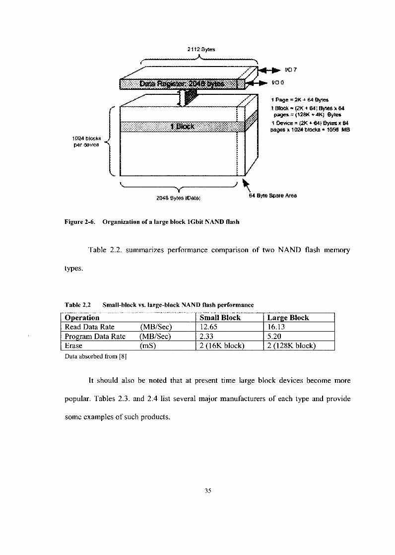
Figure 2-6. Organization of a large block lGbit NAND flash
Table 2.2. summarizes performance comparison of two NAND flash memory
types.
Data absorbed from [8]
Table 2.2 Small-block vs. large-block NAND flash performance
It should also be noted that at present time large block devices become more
popular. Tables 2.3. and 2.4 list several major manufacturers of each type and provide
some examples of such products.
Operation Read Data Rate (MBISec) Program Data Rate (MBISec) Erase (ms)
Small Block 12.65 2.33 2 (1 6K block)
Large Block 16.13 5.20 2 (128K block)

Table 2.3: Small-block NAND flash devices
Manufacturer
Table 2.4: Large-block NAND flash devices
Infineon STMicroelectronics Samsung Toshiba
Parameters
I Hynix I HY27UF 1 1Gbit (~81x16) I 1.8V, 3.3V I 48-TSOP I
Part No
HYF33DS512 NAND0 1 G-A K9KlGO8UOB TH58 100FT
Manufacturer
Samsung
Size
512Mbit (~81x16) 1 Gbit (x81x 16) 1 Gbit (x8) 1 Gbit (x8)
Parameters
Micron Infineon
I Toshiba I TH58NVGl S3A [ 2Gbit (x8) 1 2.7 ... 3.6V I 48-TSOP I
Voltage 1 Package
Part No
2.3.1.4 Multilevel Flash Memories
In Flash memories similar to any other type, density defined as number of bits per
unit area and cost per bit represent the man characteristic of memory device. One of the
approaches to increase flash memory density is to use multilevel cells. As threshold
voltage of the floating gate transistor changes with the amount of charge stored, so
changes the current through the transistor. If the sensing circuit can identify different
discrete level of the current with a single step of AIccII, then it will be possible to store n
bits in a single cell as defied by formula [7]:
supplies 2.7. ..3.6V 1.8V, 3V 1.8V ... 3.3V 3.3V
MT29F2G HYF33DS 1 G
n = log2 {[(Imm - Imin)lAIce~~I + 1 } -
This approach leads to a new family of flash devices - Multilevel (ML) devices
that can benefit from storing several data bits in one cell. However, a significant
48-TSOP 48-TSOP 63-FBGA 48-TSOP
Size
2Gbit (x81x 16) 1 Gbit (x81x 16)
Voltage supplies
Package
3.3V 2.7.. .3.6V
48-TSOP 48-TSOP

advantage of density increase brings with it a set of requirements to the devices. They
are:
Recognition of different current levels within short period of time;
Accurate programming of specified amount of charge;
Capability to store specified amount of charge for significant time.
These three problems should be dealt with in presence of program and read
disturbs typical for flash memories in general and becoming a real problem in multilevel
devices.
The multilevel approach can be applied in any type of flash memory arrays.
However, while NOR memory can implement both CHE and FN principles, only FN is
supported in NAND type devices. Since one of the characteristics of the NOR flash is
presence of unselected cells during reading that can result in bit-line leakage, it is a
necessity to all cells to have a positive threshold voltage only. On the other hand, NAND
flash is more susceptible to read disturbs due to high voltages applied to unselected word
lines during reading.
Sensing circuit is a critical component of ML flash. Naturally, with the number of
levels to be sensed increases complexity of sensing circuit. On the other hand, the number
of sensing devices per bit of information decreases. Examples of different ML flash
devices are presented in Table 2.5.

Table 2.5: Commercially available ML flash devices
Manufacturer
Intel
2.3.1.5 Serial EEPROM
Infineon Samsung STMicroelectronics
In many cases, high-density and high-cost memory devices are not required but
Parameters
rather a cost-effective solution is needed. For such designs electronic industry offers bit-
Part No RD48F4444 HYF33DS 1G K8F12(13)15 M30LOR8000
serial EEPROM usually providing storage of up to 1Mbit. These devices currently exist
in 8- and 16-bit versions and support such features as word protection, block-write
Type NOR NAND NOR NOR
protection and multiple access modes. They are typically connected to the CPU via a 2-
or 3-wire interface, such as Microwire by National Semiconductor Corp., 12c (Inter-
Features 2bitlcell 2bitkell
2bitlcell
Integrated Circuit) by Philips Semiconductor, SPI (Serial Peripheral Interface) by
Motorola, etc. Data is transferred via two wires (Data In and Data Out) or one wire (Data
Size 1 Gbit lGbit 5 12Mbit 256Mbit
Inlout) synchronously with serial clock signal of up to 10 MHz. Examples of common
Package OUAD+SCSP 48-TSOP 64-FBGA 88-TFBGA
serial EEPROMIFlash devices are presented in Table 2.6.

Tab
le 2
.6:
Seri
al E
EP
RO
MIF
LA
SH d
evic
es
Man
ufac
ture
r
Atm
el
Atm
el
IC M
ic
IC M
ic
Mic
roch
ip
Mic
roch
ip
Spa
nsio
n
SS
T
ST
Mic
roel
ectr
onic
s
Win
bond
Par
amet
er
Part
No
I Siz
e I O
rgan
izat
ion
I Clo
ck
I Inte
rfac
e I M
ode
I Pac
kage
A
T24
C10
24 (
E)"
I 1 M
b ( 8
-bit
I 400
KH
z,
I Tw
o-w
ire
Seri
al 1
256-
byte
I 8
SOIC
, 8D
IP,
AT
25P
1024
(E)
.
.
AT
25FS
040
(F)
1Mb
X24
256
(E)
I
24FC
1025
(E
) I 1
Mb
I 8-b
it
I 1M
Hz
I I~
C
I 128
-byt
e / R
SOIC
, 8D
IP
4Mb
X25
128
(E)
8-bi
t
256K
b
8-bi
t
128K
b
25L
C25
6 (E
)
M25
PE80
(F)
I 8
Mb
I 8-b
it
I 5O
MH
z I S
PI
I 256
-byt
e I V
FQFP
N8,
1 MH
z 2.
1 MH
z
8-bi
t
S25F
L06
4L (F
)
SST
25V
F016
(F)
5OM
Hz
8-bi
t
256K
b
* E - E
EPR
OM
Dev
ice,
F - F
lash
Dev
ice
SPI
4OO
KH
z
64M
b
16M
b
W25
X32
(F)
SPI
2MH
z
8-bi
t
Page
Wri
te
128-
byte
I'C
8-bi
t
8-bi
t
32M
b
8SA
P, 8
LA
P 20
SOIC
Pa
ge w
rite
1
to 2
56
SPI
lOM
Hz
8SO
IC, 8
SAP
byte
Wri
te
64-b
yte
Page
Wri
te
5OM
Hz
5OM
Hz
8-bi
t
8XB
GA
, 8S
OIC
,
Blo
ck W
rite
Pr
otec
tion
SPI
14T
SSO
P 14
SOIC
, l6
SO
IC
SPI
SPI
75M
Hz
Page
Wri
te
Blo
ck W
rite
Pr
otec
tion
8SO
IC, 8
DIP
, 8T
SSO
P 25
6-by
te
Page
Wri
te
Wri
te
Prot
ecti
on
SPI
16SO
SOIC
,8W
SON
Page
Wri
te
256-
byte
Pa
ge W
rite
S0
8W
16
SOIC

2.3.2 Volatile Memory Devices
Volatile memories are devices which retain integrity of the stored data only when
continuous power is applied. There are two major groups constituting this memory type -
Static Random Access Memory (RAM) and Dynamic Random Access Memory
(DRAM). Both groups are described in the following subsections.
2.3.2.1 Static RAM
SRAM has an address-decoding scheme that allows access to any cell of the
rectangular memory array individually because every cell has a unique address associated
with it. Typically, an SRAM cell is realised as a bi-stable flip-flop made up of four or six
transistor. Four-transistor cells have been widely used for medium to high applications.
However, they are characterised by higher leakage current than their 6-transistor
counterparts. Because 6T-based SRAMs
a) have lower leakage and standby currents,
b) more stable,
c) draw significant current only when switching,
d) use substrate based transistors,
e) easier to scale in geometry
there is a tendency to migrate toward them in new designs. Two types (4T2R and 6T) of
memory cells are depicted in Figure 2.7.

Bit Line O Bit Line 1
b)
Figure 2-7. SRAM cells: a) typical 4T2R cell, b) 6T-cell
Currently, there are two types of SRAM available on the market: synchronous and
asynchronous. In synchronous SRAM devices, all operations are controlled by externally
generated clock signals. In contrast, in the asynchronous SRAM, clock signals are
generated by the internal circuit in response to the transitions on the address pins. As a
result, the latter have certain limitations at the higher end performance requirements.
Specifically, there are two most important parameters valued for the SRAM along with
the memory array size. They are access time and cycle time.
Access time is specified as the minimum time interval required to read a bit of
information from a memory cell, while cycle time is defined as time for completion a
read or write operation and reset internal circuitry so that the next operation can start.
Modern SRAM devices have access time as short as 8 ns.

2.3.2.2 Dynamic RAM
Dynamic Random Access Memory (DRAM) devices are based on charge storage
in a capacitor in contrast to Static RAM, where each cell is a bi-stable flip-flop built of
four to six transistors. In earlier DRAM devices, memory cells consisted of 3 transistor
and later they were scaled dolwn to one MOSF'ET acting as a switch. The presence of a
charge on the capacitor is recognized as logical "1" and its absence as "0". An example
of a DRAM cell schematic and its planar structure are depicted in Figure 2.8. a) and b),
respectively.
Word Line
Figure 2-8. DRAM cell: a) Sche~matic representation, b) Planar cross-section
Having compared this cell with the cell architecture of a SRAM cell, it is
reasonable to expect that a DRAM cell wnll occupy lesser space. Indeed, it is the major
advantage of this memory type, which leads to higher storage capacity per die. However,
there is price to pay for this feature. Since the DRAM cells are essentially capacitors,
charge from which can leak. away, data would be lost over time without additional
procedure of reading cells periodically and restoring the information. This operation is
called Refresh. Frequency of refresh operation depends on the manufacturing technology
and parameters of the capacitor, in particular. In most cases, a single refresh cycle is
required to restore charge along an entire row.
2.3.3 Comparative Analysis of SRAM and DRAM Devices
To compare different types of volatile memory devices a collection of presently
available chips is offered in Table 2.7. It is easily noticeable that, in general, DRAM
memory provides a designer with the following advantages:
Bigger memory arrays as per chip,
Smaller size package,
Comparable or better access time,
Single power supply.
A major disadvantage of the DRAMS is the requirement for the additional refresh
signals. However, present day CPUs usually provide complete interface for these devices.

Tab
le 2
.7:
Ran
dom
acc
ess
mem
ory
devi
ces
Man
ufac
ture
r
Mic
ron
Mic
ron
Sam
sung
S
amsu
ng
Win
bond
C
ypre
ss
Cyp
ress
IDT
ISS
I
Sam
sung
Cyp
ress
I
* A - A
sync
hron
ous,
S - S
ynch
rono
us
Par
amet
er
IDT
ISS
I
Sam
sung
MT
48L
C64
M8
K4M
5 1 1
63
K4S
1G
0732
B
W98
6416
BH
C
Y7C
1 04
9B
CY
7C10
69A
V33
IDT
71V
416
IS61
WV
2048
8
K6R
4008
VlD
CY
7C13
16A
V18
IDT
7 1 V
6760
2
IS61
LF2
5672
A
K7R
6418
82M
VD
DN
DD
Q
1.8V
Pa
rt N
o M
T48
H16
M16
SDR
AM
SD
RA
M
SDR
AM
SD
RA
M
SRA
M (A
)*
SRA
M (A
)
SRA
M (A
)
SRA
M (A
)
SRA
M (A
)
SR
AM
(S)
I
Pack
age
54-V
FBG
A,
Acc
ess/
Cyc
le
6 nS
SRA
M (
S)
SRA
M (
S)
QD
R S
RA
M
Ref
resh
64
mS - 8
K
Typ
e SD
RA
M
Org
aniz
atio
n 16
Mx1
6
64M
x8
32
M
x16
128M
x8
4M
x16
5 12K
x8
2M
x8
256K
x16
2M
x8
512K
x8
2M
x8
I 25
6K x
36
256K
x72
4M
x18
64m
S-
8K
64m
S - 8
K
64m
S-
8K
64m
S-4
K
I
5.4
nS
5.4
nS
12 n
S 8
nS
10 n
S
8 nS
8 nS
4 nS
I
3.5
nS
6.5
nS
0.45
14.
0 nS
3.3V
1.
8V
3.3V
3.
3V
5V
3.3V
3.3V
1.8V
or
3.3V
3.3V
1.8V
l1.5
V
I
54-T
SOP
I1
54-F
BG
A,
54-T
SOP
I1
54-T
SOP
I1
36-S
OJ
54-T
SOP
11,
60-F
BG
A
44-S
OJ,
44
-TS
OP
11,
48-B
GA
44
-TS
OP
11,
48-B
GA
36
-SO
J,
44-T
SO
P I1
16
5-FB
GA
I
3.3V
I2.5
V
3.3V
l2.5
V
1.8V
l1.5
V
1 00-
TQ
FP,
1 19-
BG
A,
165-
FBG
A
1 00-
TQ
FP,
1 19-
, 209
-,
165-
PBG
A,
165-
FBG
A

2.4 CPU Selection
The core processor is the central part of the Holonic Agent controller. It is
responsible for all processes taking place during the mobile network function including
data acquisition and processing, support for existing periphery and communication with
other devices. Obviously, the architecture of the processor will define the structure of the
entire system hardware. Thus, selection of the processor requires special attention and a
detailed analysis of the existing options.
2.4.1 Prototype I CPU Solutions
The previous prototype [5] was built using a PXA255 processor, a representative
of the Intel StrongAnn family. Various representatives of this family are presented in
Table 2.8. All of these devices were designed for various types of mobile applications -
including cellular phones, personal digital assistants - and provided various levels of
speed and interface capabilities.
It is easy to notice how the CPU integration level grew with progress in
microelectronic device technology - from 0.35 pm for SAllO to 0.18 pm technology
used in PXA255. On-chip facilities progressed from Cache memory and JTAG interface
to numerous sophisticated devices. However, the complexity of the packages increased
and requires higher levels of assembly and PCB manufacturing technologies.

Tab
le 2
.8:
Com
para
tive
cha
ract
eris
tics
of t
he S
tron
gArm
fam
ily p
roce
ssor
s
Yea
r
1999
200
1
2003
2005
Mob
ile
Proc
esso
r
SA
llO
SA
lllO
PXA
255
PXA
2 70
Fre
quen
cy,
MH
z 10
0,
160,
16
6,
200,
23
3
Pow
er
Con
s.m
W
<300
, <4
50,
<700
, <9
00,
<lo
o0
Pow
er
Mod
es
Idle
, Sl
eep
Nor
mal
, Id
le,
Slee
p
Idle
, Sle
ep,
Fast
Sle
ep
Wk
Idle
, Sle
ep,
Dee
p-sl
eep,
St
andb
y,
Mem
ory
Bus
, M
Hz
33,
53,
53,
66,
66
100
100
100
eter
M
emor
y In
terf
ace
32-b
it ad
dres
s
RO
M,
SRA
M,
FLA
SH,
SDR
AM
RO
M,
FLA
SH,
SRA
M,
256
MB
SD
RA
M
1 G
B
SDR
AM
, 38
4 M
B
RO
M
Cac
hes
16 K
- D
, 1
6K
-I
8K
-D,
16
K-I
32 K
- D
, 32
K-I
, 2K
-min
i D
32
K-D
3
2K
-I
2K-m
ini D
Inte
rfac
e
JTA
G
2 -
PCM
CIA
, 28
- G
PIO
PCM
CI A
, U
AR
T,
SSP,
LC
D,
12c,
PWM
, SD
IMM
C,
JTA
G,
15 -
GPI
O
UA
RT
, U
SB, 1
2c,
PCM
CIA
, M
MC
, SSP
Pac
kage
1 44-
TQ
FP
0.35
pm
256-
mB
GA
0.
35 p
m
- 25
6-PB
GA
0.
18 p
m
3 56-
VF-
BG
A,
3 60
-PB
GA
D
SIl
mm
pitc
h

Table 2.9. shows an excerpt from the datasheets and products briefs of the most
popular mobile processors currently available on the market.
All processors are built using a 32-bit architecture. Among those processors, the
Intel PXA270 can operate at the highest speed - up to 624 MHz. This feature should be
taken into account as it can reduce the response time to any request for the processor's
resources. Only AMD's Au1100 capable of running at 500 MHz stands close in oscillator
frequency.
Another important parameter of a device intended for mobile communication is
power consumption. It can be evaluated in terms of miliwatts of power per 1 MHz of
operational frequency. Applying this approach, the processors can be arranged in the
following order:
1. AUllOO
3. AUllOO PP5022
333 MHz 0.6 mW/MHz
400 MHz 0.625 mW/MHz 200 MHz
500 MHz 0.8 mW/MHz 100 MHz
250 MHz 1.0 mW/MHz
104 MHz 1.12 mW/MHz
3 12 MHz 1.25 mW/MHz 266 MHz
200 MHz 1.3 mW/MHz
8. PXA270 208 MHz 1.34 mW/MHz
9. PXA270 416 MHz 1.37 mW/MHz
10. PXA270 520 MHz 1.44 mW/MHz
11. PXA270 624 MHz 1.48 mW/MHz
PXA270 has the highest on-chip Data and Instructions cache of 32 Kbytes each
plus 2 Kbytes of 'mini' Data cache. Cache memory is intended to reduce number of
accesses to the external memory and, thus, results in higher performance. Integrated
SRAM memory in this device is also the largest of all items reviewed and equals 256
Kbytes.
Finally, the PXA270 processor has the largest addressable space for an external
memory.
A significant advantage of the NAND flash memory interface is presented by
Samsung in their S3C2410A, but quite small memory address space available for
SDRAM (256 Kbytes) can create potential difficulties at the architectural design stage.
In the decision making, an existence of at least two types of the device package -
with a considerable pitch for prototypes and with the fine one for the final product - will
play a significant role. Again, the PXA270 is ahead of others as it provides 0.5 mm and 1
mm pitch BGA packages.

Tab
le 2
.9:
Com
para
tive
cha
ract
eris
tics
of
som
e co
mm
erci
ally
ava
ilabl
e pr
oces
sors
for
mob
ile a
pplic
atio
ns
I Proc
esso
r / Ma
nufa
ctur
er
N
I Mob
ile
I-
S3C
24 10
A
Sam
sung
s
Inst
rum
ents
Par
amet
er
Freq
uenc
y, (
Pow
er
I Cor
e I A
rchi
tect
ure
I Cac
hes
I Mem
ory
MH
z C
ons.
, mW
C
ontr
olle
rs
333,
20
0,
MIP
S32
32-b
it 16
K - D
, FL
ASH
IRO
M,
8 K
- D
, A
sync
. SR
AM
I 8
K-I
FL
ASH
, Sy
nc.
SDR
AM
1 F
LA
SH
loo
1 32
-bit
8K - C
PU,
256M
B S
DR
AM
, 7
I 8K
- C
OP
25
6 M
B N
OR
200
266
I I
I I
I fla
sh
220
I I
I I
104,
208
, 1 1
16, 2
79,
[ XSc
ale
1 321
16-b
it I~
~K-D
I IG
BS
DR
AM
,
259
335
31 2,
416
, 39
0, 5
70,
384
MB
RO
M
520,
624
1 747,92
5 1
1 1 ~~
LYA
D
1 A
RM
926T
E
AR
M92
0T
1613
2-bi
t,
1613
2-bi
t, 0.
18 u
m
16 K
- D
16 K
- D
, 1
6K
-I
(NO
R o
r NA
ND
) 12
8MB
SD
RA
M,
FLA
SH
768M
B R
OM
, 25
6MB
SD
RA
M

Tab
le 2
.9. (
Con
tinu
ed)
com
para
tive
cha
ract
eris
tics
of s
ome
com
mer
cial
ly a
vaila
ble
proc
esso
rs f
or m
obil
e ap
plic
atio
ns
Par
amet
er
Inte
rnal
] P
ower
I B
us C
lk I
Inte
rfac
e I O
ther
Itte
rfac
e ] G
PIO
I P
ower
Sup
plie
s I P
acka
ge
SRA
M
-
I DTV
, LC
D, I
'S,
iRA
M
I / ~~
~~
ac
tF
la
sh
, SI
P-D
IF,
80 K
B
Mod
es
Idle
, Sle
ep
Hal
t, St
andb
y
-
MH
z 10
0,
125
160
KB
100,
12
5
Nor
mal
, Sl
ow, I
dle,
256
KB
USB
, 3-U
AR
T,
2-SD
, 2-S
SI,
PCM
CIA
Pow
er-o
ff
Stan
dby
US
B, M
MC
, S
SP
, 3-U
AR
T,
PCM
CIA
I*C
3-
UA
RT
, 2-S
PI,
USB
, I~
C,
Idle
, Sle
ep,
Dee
p-sl
eep,
St
andb
y,
1011
00 E
ther
net,
IrD
A, L
CD
, I~
S,
Con
trol
ler,
SDII
MM
C
USB
, SP
I, I'
C,
AC
97
IrD
A, A
C'9
7,
LC
D C
ontr
olle
r,
JTA
G
AT
A66
, JT
AG
Ir
DA
, LC
D, I
~S
, JT
AG
100
48/1
3'
IrD
A, L
CD
Up
to
60
117
I 2
41
~~
'
SDIM
MC
ISD
IO
UA
RT
, USB
, I~
C, PC
MC
IA,
MM
C, S
SP
1.1-
1.3V
Cor
e,
2.51
3.3
V I
10
& I1
0 1 .
05- 1
.3V
Cor
e
399-
BG
A,
17x1
7 m
m
1.8
V C
ore,
3.
3 V
I10
I10
1.8-
2.O
V C
ore,
3.
3V M
emor
y 0.
8 m
m p
itch
28
9-B
GA
LC
D, A
C'9
7,
PWM
, JT
AG
256-
PBG
A
256-
CA
BG
A
110.
8mm
itc
h
272-
FBG
A
14x1
4 m
m
12 11
2'
0.85
-155
V C
ore
2.51
3.01
3.3V
I10
35
6-V
F-B
GA
, 36
0-PB
GA
0.
51lm
m p
itch

Having compared all strength and weaknesses of the processors listed above and
taking into account such important feature as software and architecture compatibility, the
PXA270 processor has been chosen as a core device for the Holonic Controller.
2.5 Components for Wireless Interface
2.5.1 Fundamentals of 802.11 Wireless Networks
The IEEE 802.1 1 Working Group was tasked to devise a standard that would not
only support devices in a fixed location, but would also support portability and mobility.
The first version of the 802.1 1 standard was released in 1997 and offered interoperable
rates as high as 2 Mbps. The ratification of 802.1 1b standard in 1999 raised the operation
speed limit to 11 Mbps, thus, competing with wired Ethernet communication rates of 10
Mbps. Currently, the 802.11 family includes six over-the-air modulation techniques
among which a, b, and g are the most popular.
Applying this standard, WLAN equipment can be configured in three major ways.
The simplest configuration is called an Independent Basic Service Set (IBSS) or ad hoc
within which each station can directly communicate with one or more stations inside the
group. There is no centralized coordination of the group. An example of an lBSS is
presented in Figure 2.9.

Mobile Agent
Figure 2-9. Architecture of independent basic service set (IBSS)
The standard does not limit the number of the devices connected to the IBSS
network. Since each device in this network functions as a client in absence of an access
point, some of them cannot communicate directly with each other as a result of the
hidden node1. There is no mechanism provided to relay messages between such devices
either. Timing control is organized in a distributed style.
A second type of configuration, Basic Service Set (BSS), adds centralized
distribution, buffering, and gateway functionality through a device called an Access Point
(AP). In this type of network, mobile devices communicate with the Access point rather
than with each other. Since AP relays messages between stations, the area covered by
service can be effectively increased. Figure 2.10. depicts a structure of a BSS.
' A hidden node results from the situation when two stations are out of range of each other, but are in the range of the Access point.

W e Agent M* Agent
Figure 2-10. Architecture of basic service set (BSS) network type
An Extended Service Set (ESS) is a configuration with numerous BSSs acting as
a single WLAN. For this configuration, the standard introduces a mechanism called the
Distribution System (DS). This mechanism is requested to determine whether messages
are to be sent within the same BSS, passed to another AP's BSS or transmitted to an
external network [9]. The DS can be realized as a wireless link or a wired connection.
Figure 2.1 1. illustrates an architecture of an ESS type wireless network.

Figure 2-11. Architecture of extended service set (ESS) wireless LAN
Developing a hardware device for distributed wireless system, our focus will be
on the 802.1 1 PHY layer.
2.5.1.1 Principles of 802.11 WLANs
The original 802.1 1 standard defined two WLAN PHY methods:
2.4 GHz frequency hopping spread spectrum (FHSS)
2.4 GHz direct sequence spread spectrum (DSSS)

FHSS WLANs support 1 Mbps and 2 Mbps data rates in the frequency band split
into 79 non-overlapping channels between 2.402 and 2.480 GHz in North America. Thus,
the FHSS WLANs use a fast 1 MHz symbol rate hopping among the 79 channels at a
minimum rate of 2.5 times per second and must contain at least six channels. To
minimize collisions between overlapping areas, the possible hopping sequences can be
broken into three sets of length. As a result, the hopping patterns guarantee that each hop
covers at least 6 MHz minimizing probability of a collision. An example of a Frequency
Hopping pattern is illustrated in Figure 2.12.
I
Frequency 2.4.83 OW
Figure 2-12. An example of a frequency hopping pattern
To modulate data at 1 Mbps the 802.11 uses Gaussian Frequency Shift Keying
(GFSK) and for 2 Mbps operation it uses 4GPSK applying two deviation frequencies as
shown in Table 2.10.

Table 2.10: Symbol to frequency mapping in 4 GPSK
There are, however, certain disadvantages pertaining to FHSS modulation [lo]:
Transmitted Symbol 00 0 1 10 11
Relatively low data rates
Mapping Frequency FC - Fd1 FC - Fd2 Fc + Fd2 Fc + Fdl
Significant sensitivity to interference spread over a set of channels in the
Fc - Carrier Frequency; Fd - deviation frequency
frequency band
Absence of mechanisms to synchronize hopping sequences of separate
pairslgroups of communicating devices.
As an alternative to FHSS, DSSS supports 1 and 2 Mbps data rate in the original
802.1 1 standard and provides higher communication speed of 5.5 and 11 Mbps in
802.11b. WLANs using DSSS technique operate in 3 non-overlapping channels 22 MHz
each (see Figure 2.13.). Every single bit of 1 Mps data stream is encoded and converted
in to 11 MHz chip stream (a binary 1 expands to 11 11 11 11 11 1 and 0 to 00000000000)
and then XORed with a spreading sequence. Thus, a bit of information represented by 11
bits of code and then spread over 22 MHz-wide channel can suffer very little impact by
the interference.
To transmit data at 1 Mbps rate the DSSS WLANs use Differential Binary Phase
Shift Keying (DBPSK) and Differential Quadrature Phase Shift Keying (DQPSK) to
transmit at 2 Mbps rate.

Figure 2-13. Three non-overlapping channels of the DSSS 802.11 WLAN
DBPSK operates as follows: Each chip maps into a single symbol. A. 0 tells the
symbol mapper to transmit the same symbol as in previous session while 1 orders it to
rotate the phase by 180 degrees. The same principle is applied in DQPSK to achieve 2
Mbps data rate, but each symbol is represented by two chips providing 4 possible
combinations of phase rotation as shown in Table 2.11.
Table 2.11: Chip to differential phase mapping in 4 ISQPSK
I Chip Mapped To Symbol -%&e Change =I
2.5.1.2 Principles of 802.llb WLANs
To achieve higher data rates of 5.5 and 11 Mbps, 802.11b employs
Complementary Code Keying (CCK) or Packet Binary Convolutional Coding (PBCC)
modulation.

To transmit using CCK modulation, the scrambled bit stream is grouped into 4-bit
or 8-bit sets for 5.5Mbps and 1 lMbps, respectively. First two bits (bO and bl) define four
phase rotation states for odd symbols and four - for even symbols. The latter two or six
bits - depending on the speed - determine the complex chip sequence. There is one
sequence in case of 5.5 Mbps (4 bit) and 64 possible sequences when llMbps
mechanism is used. The resultant sequence modulates the appropriate carrier frequency.
To transmit using optional PBCC modulation, the scrambled bit stream passes
through the six-delay element half-rate binary convolutional encoder that outputs two bits
for every one input bit. The encoded bit stream then passes through a BPSK symbol
mapper or QPSK symbol mapper to achieve 5.5 Mbps or 11 Mbps, respectively. The
particular symbol mapping depends on the binary value coming out of a 256-bit pseudo-
random sequence.
2.5.2 Multipath Loss
Usually, in a wireless environment, the communicating devices are not located in
a line of sight. Obstacles surrounding transmitting and receiving stations can create
multiple reflections of original signal, resulting in the situation when signal can come
from different directions with different strength at different time points. The important
path is the direct path while the non-direct paths are the sum of reflections from
reflections off various surfaces. This phenomenon is depicted in Figure 2.14.

Carrier ~ ~ u l a t e d RF Signal Received
after Mullipath Signal ReA&ns
Direct Signal 7 , XMitter +
f
. . . . - .
Figure 2-14. Multipath signal propagation
- - . . - -
The resultant signal can be seen as a total of direct signal
- Data Modulated by
- - - ReudoRandom Sequem frwn Direct Path
- - - i
where T represents the signal delay after propagation and
and multipath signal:
TI < T2.
- - - -
If the delay between these two signals is greater than the chip duration, the
secondary multipath signals are not synchronised and not correlated with the receiver's
de-spreader code and do not cause interference with the direct signal and in most cases
appear as additional noise into the receiver [I 11.
- - - - - - . -
Delayed signals that are not in sync with the internal code can be adaptively
synchronised and added to the receiver's performance. For this purpose a RAKE receiver
can be employed that detects the strongest multipath signals from the received and aligns
them with the code. It is designed to separately receive, process and combine multiple
signals so that they contribute to the output. For an 802.1 1b network, where chip duration
is approximately equal 90 ns, the multipath signals should be separated in arrival time by
this interval for the RAKE receiver to be effective.
Directly related to the RAKE receiver application in coping with multipath
phenomenon is the diversity antenna solution. The receiver supporting two antennas -
main and auxiliary - monitors both of them and chooses the one receiving stronger
signal. There are three generic approaches to antenna diversity that have proved to be
very effective for mobile radio stations:
Antenna separation (Spatial),
Polarisation,
Pattern, or Angle.
Spatial diversity is based on two or more antennas separated in space. In a
multipath environment, each antenna experiences different degrees of fading. Thus, it is
possible that when one antenna is in deep fade another one is not and provides effective
reception. It has been proved that antenna spacing as small as 1/10 of a wavelength can
provide sufficient diversity gain [12]. When the Polarisation diversity is applied, the
antenna(s) provide dual orthogonal polarisation. In the case of Pattern diversity, multiple
directional beam antennas are used. The second approach is most effective in applications
for both transmission and reception of the base stations, while the first and third are more
affordable and easy to implement in the mobile devices.
2.5.3 Wireless Platform Analysis
There are several complete 802.1 1 solutions currently available in the market.
Some of the devices are advertised as System-in-Chip (Sip) and their most important
parameters are collected in Table 2.12.

It should be noted that a number of alternative solutions exists, but for this project
development the main interest was toward single-chip wireless configurations. The
802.11 device should contain a complete transceiver along with a baseband processor in
one package and a number of common communication interfaces needs to be supported
to provide high-speed connection with the Host. (In this case, a Mobile Agent Controller
and its CPU are considered to be Host). The minimum number of external parts required
is an essential advantage. The last important criterion is a relatively small package which
would not set high-level requirements for the printed board design and technology and
would allow easy access for rework at the prototyping stage.

Tab
le 2
.12:
C
omm
erci
ally
ava
ilabl
e sy
stem
-in-p
acka
ge 8
02.1
1 So
luti
ons
Man
ufac
ture
r I P
art Ng
Bro
adco
rn
Phili
ps
I BGW
2OO
Tex
as
TN
ET
W-
Inst
rum
ents
Inte
rfac
e I Mo
dula
tion
QPS
K, C
CK
, U
AR
T
16/6
4 O
AM
, D
BPS
K, D
QPS
K
SPI,
C
CK
, DQ
PSK
, SD
IO-1
or
DB
PSK
4
wir
e
SPI,
SD
IO-1
or
4 w
ire,
PCI,
CF+
, ( O
FDM
CC
K, D
QPS
K,
DB
PSK
UA
RT
C
arB
us,
USB
,
CC
K, P
BC
C,
Par
amet
er
Sta
ndar
d S
yste
m B
us
I
802.
11bl
g I E
EPR
OM
802.
1 1b
PCM
CIA
,
Com
pact
Fl
ash
Seri
al
EE
PRO
M
802.
I 1 a/
b/g
PCM
CIA
-7
Fre
quen
cy
Ban
d, G
Hz
2.3-
2.5
Pow
er
Pac
kage

3 HCS HARDWARE DESIGN
3.1 Functional Design
The block-diagram of the holonic hardware unit is depicted in the Figure 3.1.
Holonic Transceiver
Holonic Transceiver rI
Holonic Controller
I
PCMCIA Device
Figure 3-1. Architecture of the holonic mobile agent
The Holonic Communication System (HCS), also referred as a Mobile Agent,
consists of two separate types of devices -Controller and wireless communication units.
The communication unit provides transmission and reception of data via a RF medium

with the application of the 802.1 l b network link operating in the band between 2402 and
2497 MHz. In order to increase data throughput of the device communicating with
several other units simultaneously, 3 independent channels are provided which support a
802.1 1b MAC layer with a maximum raw rate of 11 Mbit/sec each, resulting in overall
bit rate of 33 Mbitlsec. Thus, each holon can connect to up to three virtual networks.
Each of the three communication channels is built as an independent circuit board
incorporating a conventional 802.1 l b transceiver device in a typical configuration.
Communications between the HCS Controller and HCS Transceivers is realized
using an SPI interface, where the Controller acts as a Master and Transceivers are Slaves.
To provide effective control of the mobile agent from a personal computer (PC)
during the regular operation process and at the development stage the USB interface is
supported to provide communication with a PC for program loading and data acquisition.
In addition, a JTAG connection is included in the design to support in-circuit debugging
and periphery monitoring during the hardware troubleshooting.
Optionally, a PCMCIA memory card, or another device capable of
communicating through this bus, can be connected via the dedicated port for data storage
and application update during mobile operation.
3.2 Memory Selection
Since the Controller board size directly depends on the number of memory chips,
an attempt to utilize the highest available density devices was exercised. Each device
selected is the highest density representative of its type among the commercially
available memory.

3.2.1 NOR Flash
To provide highest density for the required NOR flash memory array, Intel's
StrataFlash devices were chosen. This family consists of devices between 64 Mbit and 1
Gbit. The high level of density is achieved by implementation of multilevel principle
providing 2 data bits per cell. It operates at 1.7 - 2.OV Core voltage and 1.7 - 3.6V for
110s providing a wide range of flexibility in interfacing with various processors.
3.2.2 NAND Flash
As a basic element of NAND flash array, a Micron's MT29F family was selected.
These devices are available in densities from 1 Gbit to 8 Gbit in 48-pin TSOP packages
that guarantee good adaptability should larger NAND array be required for further
development. These large-block devices operate at voltage range from 2.7 to 3.6 V and
guarantee data retention for 10 years.
3.2.3 SDRAM
The Samsung 1 Gbit SDRAM from the K4SlG0732 family was the most suitable
for the design. It is supplied in a 54-pin TSOP package and operates at frequencies up to
133 MHz from standard 3.3V power supply.
3.3 Detailed Hardware Design
3.3.1 Architecture of the HCS Controller
The block-diagram of the holonic mobile controller is presented in Figure 3.2. An
Intel PXA270 microprocessor for mobile and handheld devices is used as the Core
processor. Different representatives of this family of processors can to operate at speeds
up to 600 MHz, but for the prototype a 420-MHz device was chosen. System memory is

organized in three functional arrays. The first array is a 1GByte NOR Flash connected to
16 bit data bus for boot application during start-up. Since such a memory volume is not
supported directly by the Core processor, NOR Flash is addressed as 4 pages selected by
the application. The application stored in NOR flash is unpacked and loaded into the 16
bit SDRAM upon the system initialization, from where it will be running at the stage of
regular operation. The SDRAM array is built of 8 single chips, 1 Gbit each arranged in
16-bit words. Finally, the third array is a NAND Flash segment designed to store large
volumes of data during the system operation. This partition consists of 4 devices, 2 Gbit
each arranged in 16-bit words. Since a dedicated interface in the Core processor for this
type of memory does not exist, the control signals for it are provided via the GPIO ports
of the processor.

CORE Processor
Figure 3-2. Architecture of the holonic mobile agent controller
3.3.2 Architecture of the HCS Transceiver
The Holonic Transceiver is built on a Philips BGW200 802.1 1b plug-and-play
System-in-Package (SIP) that provides a complete PHY and MAC solution for embedded
and mobile application. The architectural diagram of the transceiver can be seen in the
Figure 3.3 . The 802.11b SIP includes all baseband and RF functionality and requires
oilly exfernal antennas and external reference clock. The SPI interface can operate in two
differer! 1~3des - I S a host and as a slave. The former mode is used to communicate with

an optional serial memory device externally connected to the Sip at the data rates of up to
66 Mbps.
802. I I b Sip Senal FLASH 1 Mb~t
Figure 3-3. Architecture of the holonic mobile agent transceiver
When configured as a slave the Sip is capable of communicating with a host
(Mobile Agent Controller).
The Transceiver has its own JTAG in-circuit emulation interface and can be
controlled through it during development independently from the Controller. Two
antennas placed at distance of approximately % of wavelength should provide effective
antenna diversity.

3.4 Electrical Circuit Design and Analysis
3.4.1 Characteristics of R4icro-controlller
The major blocks of the PXA270 Architecture that present special interest for the
current design are shown in the Figure 3.4.
Figure 3-4. Rlocks of the PXA2'70 processor essential for HCS controller design
This device has sufficient internal memory and will be able to control 3 units of
HCS Mobile Transceiver. The on-chip periph~ery will be used to connect 1:o specified
memory arrays and interfaces.

3.4.2 Design Challenges
To realize the described architecture as a hl ly hnctional device it will be
necessary to cope with several challenges arising during the design process. The
following paragraphs describe the problems that required special considerations. The
most important are inadequate supported memory space, absence of a direct NAND flash
interface and high-speed signals used in the design.
Inadequate memory address space
One of the major challenges arose when attempting to connect memory arrays to
the core processor that is not intended to address such large spaces. According to the
PXA270 datasheets, the device can directly address 1 GByte SDRAM array divided in 4
banks, 256 MBye each. However, the processor can operate only with 4 banks of
synchronous FLASH memory, where first 2 banks can be up to 128 Mbytes and other 2
banks can be up to 64 Mbytes each, yielding 384 Mbytes of FLASH memory in total.
This is significantly less than required by the design specification and needs a solution.
NAND FLASH is not directly supported
Even though the PXA270 processor is capable of operating with different types of
memory devices including SDRAM, static RAM, ROM and synchronous FLASH,
unfortunately, there is no dedicated interface to NAND FLASH devices. Intel offers a
solution to overcome this deficiency by adding a few components to the design and
converting the PCMICIA interface into NAND FLASH control bus [13]. However, the
proposed solution interferes with the design specification that reserves the PCMICIA
interface for potential usage of memory cards and other periphery supporting this bus.

Presence of High-speed signals on the board
As mentioned above the selected core processor can operate at clock frequencies
up to 624 MHz. SDRAM and NOR FLASH devices can run at clock frequencies of 133
MHz and 40 MHz, respectively [12, 131. These signals create a potential for Electro-
magnetic interference (EMI) and malfunction of the entire device. Special considerations
are required to eliminate this issue and make design robust.
3.4.3 Design Solutions
An important characteristic of the PXA270 memory interface is that all devices
share the same address bus and memory bus. Since the memory devices along with the
Core processor constitute the central part of the Controller, an arrangement and
distribution of the memory control resources is the most important part of the hardware
design. The HCS Controller memory map is described in Table 3.1.
3.4.3.1 SDRAM Design
Detailed design of the system started with organization of the SDRAM memory
array - the best matching portion between the processors' architecture and specification.
SDRAM address space of PXA270 exactly matches 1 Gbyte specified by the design
requirements. This array is physically created by 2 banks, each consisting of four lGbit
(128Mx8bit) chips arranged in 32-bit words. The architecture of the SDRAM memory
array is depicted in Figure 3.5.

W M I
DQMP
DQM3 -
Figure 3-5. SDRAM array organization
Every SDRAM chip has two internal banks selected by bringing pins CSO or CSl
to low voltage level [14]. Each of four (nDCSO.. .nDCS3) signals selects a corresponding
bank inside the chip consisting of four chips ,and combining their 8-bit outputs into a
single 32-bit word. Thus, from the system interface point, there are four banks 512 Mbit
each. It is also possible to mask any of four bytes of the data word by applying a DQMn
signal to a memory chip responsible foir the masked eight bits. For the electrical
schematics of the SDRAM section, see Appendix A.

3.4.3.2 NOR Flash Design
It is somewhat more complicated to provide a lGbyte memory of NOR flash
devices, since, as it was shown above, the processor directly supports only 38,4 Mbytes of
ROM.
NOR-C
Figure 3-6. NOR flash array organization
For this purpose, a Chip Select sigpal decoder was introduced into 1;he system.
(Refer to U13 in the schematic diagram in Appendix A.) Two chip select signals
(NOR - CSO and NOR - CS1) are applied to the decoder from the PXA270 processor and
used as least significant bits (LSB), whereas two most significant bits (MSB) are taken
from GPIO pins of the processor (signals NOR -- BANK0 and NOR-BANK1). Figure 3.6.

depicts the architecture of the NOR Flash army (refer to [15]). Since the entire 32-bit
word is being written or read at a time, two lowest address bits are not used. On the other
hand a GPIO configured as an output is applield to the NOR memory as A26 address bit
to provide access to all address space of the memory devices.
As a result of this configuration, 1 Gbyte of NOR Flash occupies only 256 Mbyte
address space of the processor and allows the last two nCS pins to be used to address
other memory devices. For the electrical schematics of the NOR flash section, see
Appendix A.
3.4.3.3 NAND Flash Design
NANID flash shares thle same data bus with the other types of memory. However,
it does not require address blus and receives all address information throu:sh the data
interface. Figure 3.7 presents organization of the NAND flash array in the system.
Figure 3-7. NAND flash array organization

Tab
le 3
.1:
HC
S co
ntro
ller
mem
ory
map
Add
ress
C
PU (
Sche
mat
ic)
Con
trol
Sig
nals
V
alue
0 0 0 0 1 0 0 0 1 0 1 1
Mem
ory
Spac
e M
emor
y T
ype
NO
R F
lash
NO
R F
lash
Dev
ice
u5
U
6
u5
U
6
Mem
ory
Dat
a B
its
I Devic
e C
ontr
ol
CSO
(N
OR
-CSO
) N
OR
-BA
NK
0 (G
PI0
58)
0...
15
128M
byt
es
Sign
als
n0
r0
NO
R~
BA
NK
1 (G
PI0
59)
CSO
(N
OR
CSO
) 12
8M b
ytes
N
OR
BA
NI&
(~
~b
58
)
NOR-
BAN
K^ (G
PI0
59)
CSO
(N
OR
-C S
O)
NO
R-B
AN
K0
(GP
I058
) N
OR
BA
NK
l (G
PI0
59)
CSO
(N
OR
-CSO
) N
OR
-B A
NK
O (
GPI
O5 8
) N
OR
BA
NK
l (G
PI0
59)
l28M
byt
es
NO
R F
lash
l28M
byt
es
NO
R F
lash
NO
R F
lash
C
S 1
(N
OR
-CS
1)
NO
R-B
AN
K0
(GP
I05 8
) N
OR
BA
NK
l (G
PI0
59)
CS
1
(NO
R-C
S 1)
N
OR
-BA
NK
0 (G
PIO
5 8)
NO
R B
AN
Kl
(GP
I059
) C
S 1
(N
OR
-CS
1)
NO
R-B
AN
KO
(G
PIO
5 8)
NO
R B
AN
Kl
(GP
I059
) C
S 1
(N
OR
-CS
1)
NO
R-B
AN
K0
(GP
I058
)
128M
byt
es
l28M
byt
es
NO
R F
lash
128M
byt
es
NO
R F
lash
128M
byt
es
5 12
M b
ytes
NO
R F
lash
NA
ND
Fla
sh

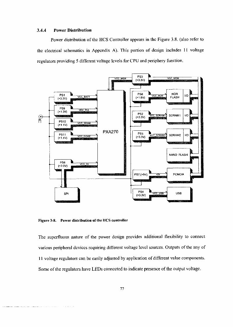
3.4.4 Power Distribution
Power distribution of the HCS Controller appears in the Figure 3.8. (also refer to
the electrical schematics in Appendix A). This portion of design includes 11 voltage
regulators providing 5 different voltage levels for CPU and periphery function.
Figure 3-8. Power distribution of the HCS controller
The superfluous nature of the power design provides additional flexibility to connect
various peripheral devices requiring different voltage level sources. Outputs of the any of
11 voltage regulators can be easily adjusted by application of different value components.
Some of the regulators have LEDs connected to indicate presence of the output voltage.
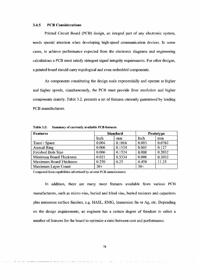
3.4.5 PCB Considerations
Printed Circuit Board (PCB) design, an integral part of any electronic system,
needs special attention when developing high-speed communication devices. In some
cases, to achieve performance expected from the electronic diagrams and engineering
calculations a PCB must satisfy stringent signal integrity requirements. For other designs,
a printed board should carry topological and even embedded components.
As components constituting the design scale exponentially and operate at higher
and higher speeds, simultaneously, the PCB must provide finer resolution and higher
components density. Table 3.2. presents a set of features currently guaranteed by leading
PCB manufacturers.
Composed from capabilities advertised by several PCB manufacturers
Table 3.2: Summary of currently available PCB features
In addition, there are many more features available from various PCB
manufacturers, such as micro-vias, buried and bIind vias, buried resistors and capacitors
plus numerous surface finishes, e.g. HASL, ENIG, Immersion Sn or Ag, etc. Depending
on the design requirements, an engineer has a certain degree of freedom to select a
number of features for the board to optimize a ratio between cost and performance.
Features
Trace / Space Annual Ring Finished Hole Size Minimum Board Thickness Maximum Board Thickness Maximum Layer Count
Standard Inch 0.004 0.006 0.006 0.02 1 0.250 30+
Prototype mm 0.1016 0.1524 0.1524 0.5334 6.25
Inch 0.003 0.005 0.008 0.008 0.450 3 0 t
mm 0.0762 0.127 0.2032 0.2032 1 1.25

3.4.5.1 Holonic Mobile Agent Controller PCB Design
The very first step in creating any PCB design is to define a layer stack-up that
represents a sequence of electrical and non-electrical layers required for the board
manufacturing. Electrical layers are typically divided onto signal layers on one side and
power and ground planes on another separated by the layers of insulator referred as Core
and Prepreg.
To achieve high level of impedance control for high-speed nets it is recommended
to place them in the signal layer located next to the constant potential planes. Such a trace
placed in an external layer nearby a single plane is called a microstrip, while a trace in an
internal layer sandwiched in between two planes is addressed as a stripline. For the best
performance, the most sensitive nets carrying high-frequency signals are recommended to
be designed as srtiplines.
Following Intel's recommendations for PCB design for the PXA270 processor
[16], the Holonic controller board is organized as an 8-layer stack-up, as shown in Figure
3.9. and consists of 2 external signal layers - Top and Bottom - also used to assemble
components on both sides, two ground planes, two internal signal layers used for clocks
and other high-speed signals, and two power planes providing all power levels for the
processor, memory devices, and periphery. However, to avoid an advanced and
potentially expensive feature as microvia and have more signal layers placed between the
reference planes, the layer assignment was slightly modified.
There are two major rules for layers assignment in a high-speed PCB stack [17]:
1. Each signal layer carrying high-speed traces should have
reference to a plane.

2. Every powes- supply must have a parallel power-gro'und pair.
Since in a PCB of such complexity as the HCS Controller high-speed traces can
occupy all signal layers, in this design all signall layers can create microstrips or striplines
for signal integrity reasons. Considering a significant number of power supplies required
for the controller, it was not possible to provi~de an individual layer for each of them.
However, each of power domains there are is presented by a copper poIygon in one of
two dedicated planes.
. . ~ - - . - . -
S i q d l --+ GND1 [ M E ] +
Sig1d2 -+ KC-I0 [Mulhple Nets]] --,
VCC-CORE [Mulhple Nets]] + S i p d 3 -+
GN D2 [WE] + S i p d 4 +
Figure 3-9. HCS controller 8-layer board layel- stack-up
To provide fault-free layout without applying for the leading edge PCB
technologies the PBGA 23x23 mm package olf the processor with 1 rnm pin pitch was
chosen. This choice allows fix the escape routing using 0.005" traces with 0.004" space
without application of microvias. A fragment of the routing area for the processor is
depicted in the Figure 3.1 O.a. It is worth to notice that there are no vias placed inside the
components pins; this makes the design acceptable by a significantly larger number of

manufacturers and guarantees significantly lower failure rate for higher product
reliability.
Figure 3-10. Escape routing for the PXA270 (a) and NOR Flash (b) on the top layer
Even a greater challenge for routing is presented by the NOR flash chips that
feature 0.8 mm pin pitch in their BGA package. One of the routing segments is depicted
in Figure 3.10.b. These two devices essentially define the design rules for the board that
are summarized in the Table 3.3
Table 3.3: Design rules for the holonic controller PCB
Features Values Inch I mm 1
Minimal Signal Trace Width / Space Minimal Power and Ground Trace Width Signal Via / Hole Power and Ground Via / Hole Minimum Space Between Polygon Planes Number of Layers
0.005 / 0.004 0.010
0.10 16 / 0.1270 0.25
*Composed from capabilities advertised by several PCB manufacturers
0.01 8 / 0.008 0.025 / 0.013 0.025 8
0.4572 / 0.2032 0.6350 / 0.3302 0.6350

Signal Integrity Analysis
Propagation Delay
As it is well known, the propagation speed of an electromagnetic signal in a
conductor in presence of a dielectric is not equal to speed of light anymore. It is rather
characterised by propagation delay that is defined as follows in pslinch for microstrip:
and for stripline in pslinch:
where Er is the dielectric constant of the insulator near conductor. Typical value of E, for
prepreg is 4.5 and for core is 4.8. Substituting E, by its value for prepreg in (1) results in
propagation delay for traces on the Top and Bottom layers equal to:
For the inner signal layers, which are surrounded by insulators with different E, an
approximation formula helps to find the resultant dielectric constant [18]:
Er = GI .VI + G2 .V2,
where and ~2 are dielectric constants for two adjacent insulators and
V1 and V2 - volume fractions of the insulators.
Assuming that both prepreg and core are of the same thickness, V1 = V2 = 0.5.
The resultant dielectric constant of the insulators surrounding traces in the internal layers
can be found as:

Applying this value in Eq(2) the propagation delay in the internal signal layers is:
tpd (stripline) = 183.3 pslinch.
Electrically Long Traces
An electrically long trace is defined as a trace in a specified layer in which (trace)
a signal transition time from (low to high or from high to low state) is greater than double
propagation delay:
t, L,, = --------
%-I
For the PXA270 processor, the shortest falllrise time is given for the SDCLK - 0
(SDRAM) signal and equals 0.5 ns [16].
Thus, using this value and data for propagation delay found above, the electrically
long trace on the Top and Bottom layers
Similarly, the electrically long trace value can be found for the internal layers as:
These results imply that high speed traces longer that 1.75" in the external layers
and 1.36" in the internal layers require signal integrity analysis, and, most likely,
application of impedance matching techniques. Obviously, it is not possible with the

existing technologies to route a data, address, or control bus between the processor and
eight SDRAM chips while having connections shorter than calculated lengths.
Trace Impedance Calculations
Trace impedance for the external layers can be calculated with the following
formula for microstrips:
where H is height of the dielectric (H = 0.2mm (7.874 mil) for prepreg in the stackup),
W is the trace width (W = 0.127mm (5.0mil)),
T is the thickness of the copper trace (T = 0.018mm (0.709mil)), and
E, is the prepreg dielectric constant equal 4.5.
For the given board parameters, the trace impedance in the outer layers is equal:
For the inner layers, formula for stripline impedance calculation can be applied:
For the approximated value of E, = 4.65 found earlier and the same board
parameters:

Driver's Output Impedance
This impedance can be approximately estimated as ratio between the low-level
output voltage of the driver and current supplied at this state:
As it can be found from the datasheet for PXA270, it can drive a load not higher
than 4 rnA when the output level of the memory bus signals is 0.3V. Thus, the driver's
output impedance will be equal:
To minimize signal reflection from the source, the load impedance ZL should
match the impedance of the driver. The reflection coefficient can be found by applying
the following formula:
where ZL is the total line impedance. Since the input impedance of the receiver is
significantly high (100KSZ and above) comparing to the line impedance, the reflection
coefficient for the receiver is typically equal 1. However, it is possible to reduce
considerably the reflection coefficient at the source. It can be easily noticed that to keep
KR = 0, it is necessary to have ZL = ZO. (In this case, load impedance is presented by Z,.
Comparing values of Zo found for outer and inner layer, it is obvious that the signals
require no or small value termination resistors (in the range of 20 SZ).

Holonic Controller PCB Physical Layout
The most critical part of the electronic design proposed for the Holonic Controller
Hardware implementation is the memory address and data bus and control signals. Not
surprisingly, the same portion is very demanding in terms of the PCB design, especially
the high-speed clock signals. There are two major types of topologies used for the
memory bus layout. Both of them have their own advantages and weaknesses.
First, the most common topology for memory devices layout is a Daisy-Chain.
This technique is very convenient because all traces go from the driver to all memory
chips on the board sequentially following the same pattern.
Advantages:
- Easy to layout,
- Traces are usually of the same length.
Weaknesses:
- Uneven signal distribution between the closest and farthest devices in the
chain,
- Performs poorly for different packages in one design.
The other common topology is the Tree:
Advantages:
- Easy to provide equal distance to each device in the bus,
- Traces are usually of the same length.
Weaknesses:

- More complex for routing,
- More board space consuming.
To provide good signal integrity for the high-speed signals on the b'oard it was
decided to implement the Tree type topology with double-side mounting. This approach
requires symmetric placement of the same type chips that would guarantee balanced load
at any moment of external memory operation cycle.
PCMCIA Buffers
Figure 3-1 1. Memory components placement on the board
The diagram of the memory devices layout on the board and their connections are shown
in Figure 3.11. At the same time, it is crucial to have as few layer switches - that result in

vias - per trace as possible. It is well h o w n that vias and soldering instants create points
of reflection that cause signal distorting and degrading and should be used with caution in
high-speed designs. It is implortant to remember that [19]:
- Properties of a via are changed by the parameters of the trace to which it is
connected.
- A via adds incremental shunt capacitance and incremental series inductance to
a trace.
- Long dangling vias can create points of resonance, aggravating the effects of
its capacitance.
- Vias that pass tlirough the same space between two reference planes (stripline
cavity) create crosstalk.
Figure 3-12. 3D model of the top side of the controller board
8 8
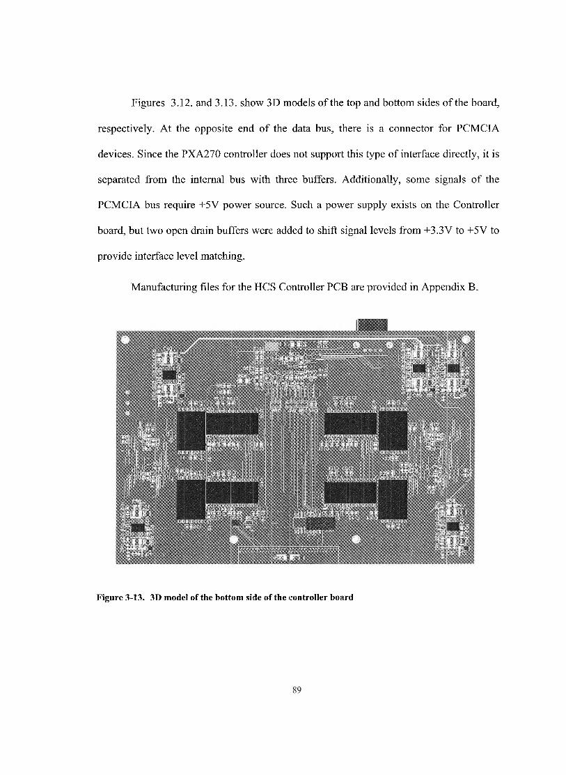
Figures 3.12. and 3.13. show 3D models of the top and bottom sides of the board,
respectively. At the opposite end of the data bus, there is a connector for PCMCIA
devices. Since the PXA270 controller does not support this type of interface directly, it is
separated from the internal bus with three buffers. Additionally, some signals of the
PCMCIA bus require +5V power source. Such a power supply exists on the Controller
board, but two open drain buffers were addled to shift signal levels from +3.3V to +5V to
provide interface level matching.
Manufacturing files for the HCS Colntroller PCB are provided in Appendix B.
Figure 3-13. 3D model of the bottom side of the tontroller board

3.4.5.2 Holonic Mobile Agent Transceiver PCB Design
The RF Transceiver printed circuit board is relatively simple compared to the
Controller. Considering usage of the System-in-Package (Sip) device for the 802.1 1b
physical layer, it is possible to realize the entire RF module in a two-layer single side
mount PCB. A layer stackup for this board is presented in Figure 3.14.
Even though power for this module is provided by the Controller board, this
device is accompanied by its own power supply located on the bottom side to give more
freedom at the prototyping, troubleshooting and firmware development stages. This
option will allow to connect periphery devices with power requirements different from
those available from the main board.
Core (12.6rriD
TOP Layer 4
Bottom Layer 4
Figure 3-14. HCS transceiver 2-layer board layer stack-up
Antenna diversity was implemented in this design by including two SMD
antennas on the PSB with 180•‹ mutual orientation. Thus an attempt to realize both spatial
and pattern diversity took place. Schematic Diagram and PCB design layers can be found
in Appendices C and D, respectively.

3.5 Comparative Analysis of Prototype I and Prototype I1 Designs
Two designs of the mobile agent for the distributed wireless network served for
different purposes at different stages of the entire system development. Prototype #1 [5]
had to provide an initial development platform and included number of peripheral devices
to support potentially needed communication mediums and interfaces. Thus, the scope of
the first prototype design was to provide as wide variety of peripheral interfaces and on-
board devices as possible rather than to focus on high performance of some of them. In
contrast, the Prototype #2 developed by this project is intended for already defined usage
and has to provide high level capabilities but for a limited number of features. In
addition, while it was sufficient for the first prototype to simulate the communication
interface with an SD-Card, the current device is expected to communicate via real
wireless interface implementing an 802.1 1b link. Table 3.4. offers a summary of the
features supported by each of two designs.
Table 3.4: Comparative characteristics of Prototype #1 and Prototype #2
Features I Prototype #l I Prototype #2 I Core Processor Highest device frequency SDRAM NOR Flash NAND Flash
PXA255 400 MHz
128 Mbytes
USB PCMCIA
PXA270 640 MHz
1 Gbyte 128 Mbytes
0
Video Out Keyboard & Mouse SPI
RS232 Yes No 1
1 Gbyte 1 Gbvte
No Yes
LED Indicators JTAG
Composed from capabilities advertised by several PCB manufacturers
Yes Yes
Yes Yes No
No No 3
6 Yes
6 Yes

4 MANUFACTURING TESTING QUALITY CONTROL
4.1 Design for Manufacturing
It was one of the major requirements to create a design that would have no, or
very little, added cost resulting from special equipment or processes. Even though, the
board is designed for double-side assembly, there is no further complexity involved in
manufacturing. The guidelines having been followed can be summarised as:
All parts of the same type are oriented in the same direction.
All components are placed and soldered using automated processes.
The PCB has a simple rectangular shape and mounting holes are symmetrically
located.
Components on the board are available in industry-standard packages.
Most components are available from different manufacturers.
4.1.1 PCB Manufacturing Strategies
Despite the design does not require any costly or laborious processes, some
procedures have to be followed. Thus, electrical test of the bare PCB should be avoided
as the probes can cause deformation of the SMT pads. This precaution is especially
important for the BGA components. During assembly, the bottom side components
should be placed first, including DC decoupling capacitors for Core processor and
memory devices. This action will prevent ESD damage of the CPU and memories when
they are installed on the PCB.

4.2 Quality Control Criteria
PCBs with ENIG surface finish have an industry-wide problem with black pad.
Before shipping, boards for assembly all bare PCBs require quality control for this defect.
Electrostatic discharge is a well-known source of serious damage to electronic
devices. All prototypes should be properly packed and the personnel coming in contact
with the devices must wear ESD equipment at any stage of production/shipment.
4.3 Design for Testing
To simplify testing process at the developments stage as well as for potential mass
production special considerations were taken:
Board layout allows for easy access during testing.
Numerous test points are available for parameters verification.
Non-used GPIOs are connected to test points for firmware needs
LED indicators are provided for visual control
4.4 Cost Analysis
For the Alpha-build of prototypes, it was planned to order 3 units of the
Controller boards and 10 units of the Transceiver. For this purpose, quotes for bare
boards as well as for board assembly were sent to two manufacturers for each of these
two steps of work. Components for assembly were ordered from two major distributors
depending on availability. A summary of the cost estimates for the Controller and
Transceiver prototypes building are given in the Tables 4.1 and 4.2., respectively. Prices

are given in Canadian dollars per unit ordered at the maximum quantity available for
prototyping process at the vendor's facilities.
Table 4.1: Summary of the controller prototypes building costs*
Process I Purchasing I Materials Cost I PCB PCBA 1 Components Supplier 1$1216.37 1 1
PCB Vendor I1 1 1 $232.86 @, 5 I I
PCB Vendor I Tooling
Tooling I I $800.00 I I
$95.87 @ 15 $706.00
" PCB Assembly Contractor I Tooling
*Composed from capabilities advertised by several PCB manufacturers
I
$225.90 @ 3 $360.00
PCB Assembly Contractor I1 Tooling
Table 4.2: Summary of the transceiver prototypes building costs*
$31 1.67 @, 3 $645 .OO
Process I Purchasing I Materials Cost I PCB PCBA
Components Supplier PCB Vendor I Tooling
PCB Assembly Contractor I Tooline
PCB Vendor I1 Tooling
$5 1 .04
$8.84 @, 46 $200.00
*Composed from capabilities advertised by several PCB manufacturers
$6.38 @ 120 $176.00
PCB Assembly Contractor I1 Tooling
Table 4.3. presents the best and worst total cost cases per prototype unit for each
of the two devices. It was taken into account that cost of tooling will be spread over the
number if the units provided by a manufacturer at the specified price. The table also
presents the entire cost of the complete prototype unit consisting of one HCS Controller
and three HCS Transceiver.
$38.30 @ 10 $645.00

Table 4.3: Total best and worst costs per prototype unit
1 Device I Best Cost Case I Worst Cost Case I I HCS Controller 1 $1705.21 1 $2135.90 I
HCS Transceiver
Total ~ e r set
$145.35
$2141.26
$167.03
$2636.99

5 CONCLUSIONS
5.1 Achievements
The project presented in this report is a next step in the development of highly
distributed mobile wireless networks implementing a holonic architecture. It incorporated
a highly over-engineered design of the mobile agent controller and WiFi communication
module. Both parts of the mobile agent hardware were designed for realization in the
form of a prototype based on available technologies and components. Compromised
solutions have been achieved to create a system providing and consisting o f
Sufficient memory volume
High-speed CPU
Effective host interface
Wireless communication interface
5.2 Design Prospective
As it was stated in the design specification, the scope of this project was to
develop an over-engineered prototype of the Holonic Communication System hardware
that can be used as a development platform for implementation of the highly distributed
Holonic Wireless Network. However, further considerations are required to proceed to
product commercialization and mass production. A number of issues requires
optimization, including,

Presence of sleep mode for power saving
Further micro-miniaturization
User friendly interface
Cost reduction
Exploring opportunities of other communication mediums
Sleep mode is an unavoidable feature for any contemporary mobile device that is
powered from a local power supply. It is required to increase the battery lifetime by
reducing device's power consumption during the periods of inactivity. The PXA270
processor can operate in this mode, but the controller device would need the addition of a
power management IC that would monitor voltage levels and control on-b~oard power
supplies during all modes of operation, such as "All Power", "Sleep", "Deep Sleep",
"Idle", and "Standby".
Micro-miniaturization is a natural feature to provide mobility and meet high
requirements for low weight and small size. This need becomes especially stringent for
handheld devices and can be achieved by high level of integration. In the described
prototype high volume of memory arrays was achieved by placing abundant number of
memory devices on the board, even though the design incorporated the highest
integration chips offered by the advance manufacturers. Further steps would rely on state-
of-the-art unpackaged dies placed directly on the board or used for custom chips. Such
wafer level products are available, e.g., from Microchip for SDRAM and NAND Flash
devices. Also, an alternative PXA270 package (VF-BGA) can be used to occupy less

space on the board. Naturally, these improvements would require advanced technologies
in PCB manufacturing, relying on finer resolution and higher precision.
User-friendly interface is an essential part of the device targeting an application
by a human. This feature assumes a coloured graphic LCD and keypad for entering data
and receiving visual information from other entities of the mobile network. Even though
the PXA270 processor has an LCD interface, its pins are configured for SSP interface
with the Transceiver boards, and, as a result, are not available. For further designs it will
be necessary to find an optimal solution supporting both options.
Cost reduction can be achieved by implementation of a number of techniques:
a) Architecture optimization and elimination of superfluous features,
b) Utilization of the most common parts at the mass production stage,
c) Simplification of the PCB and reduction of the electrical layers,
d) Design for manufacturing (DFM) and design for testing (DFT).

APPENDICES

Appendix A: Schematic Diagrams of the HCS Controller


6k66 6 F% [ 3
2 aaaa $ c =. - 4 Ell,

Appendix B: Manufacturing Files (Gerbers) of the HCS Controller

i3 . 11 ' : 1: 4 = . f I = :. Ern - - mm. ;. = = I I : I Ill. I
I Ill. I
.I .. 8 . -- ...I...... ...I...... ==
grn, ::...= ........ ....... %,-:I .-m... .-.- ..- lrng Ern. ==
1 - I =.I. "P.. -- I - g p w = == .... .....=? !f $E ....m ..... .....a.
1 o,,.:, -- .... 1 -(I
PtlT Top Paste Hol on. GTP
Controller top solder paste layer

SST Top Overlay Hol on. GTO
Controller top silkscreen layer

SUT Top Solder Mask Hol on. GTS
B I.. I D . . -I
11 B D.. mm B I.. I- . . . . . m D = = r
Controller top solder mask layer
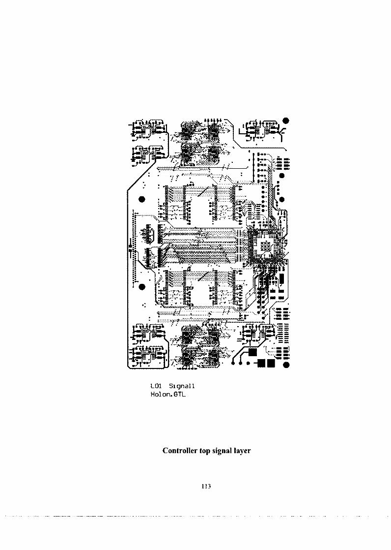
LO1 Siqnall Hol on. GTL
Controller top signal layer
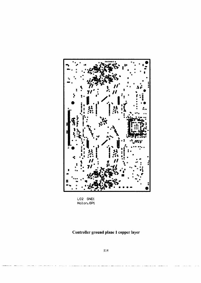
LO2 GNDl Hol on. GP1
Controller ground plane 1 copper layer

t03 Srqna12 Hal on. GI
Controller signal 2 internal layer

LO5 UCC-I0 Hol on. GP2
Controller power plane 1 copper layer

Controller power plane 2 copper layer

LO4 Slgnal3 Hol on. G2
Controller signal 3 internal layer

Controller ground plane 2 copper layer

LO6 Siqnalt Hol on. GBL
Controller bottom signal layer

SUB Bottom Solder Mask Hol on. GBS
Controller bottom solder mask layer

SSB Bottom Over lay Hol on. GBO
Controller bottom silkscreen layer

PflB Bottom Paste Hol on. GBP
Controller bottom solder paste layer

Appendix C: Schematic Diagram of the HCS Transceiver


Appendix D: Manufacturing Files (Gerbers) of the HCS Transceiver

T r anscel ver, GBL
Transceiver top (top image) and bottom (bottom image) signal layers
127

Tr anscei ver . GTO
Transceiver. GBO
Transceiver top silkscreen (top image) and bottom silkscreen (bottom image) layers

T r a n s c e i v e r . GTP
Tr anscei ver . GBP
Transceiver top solder paste (top image) and bottom solder paste (bottom image) layers
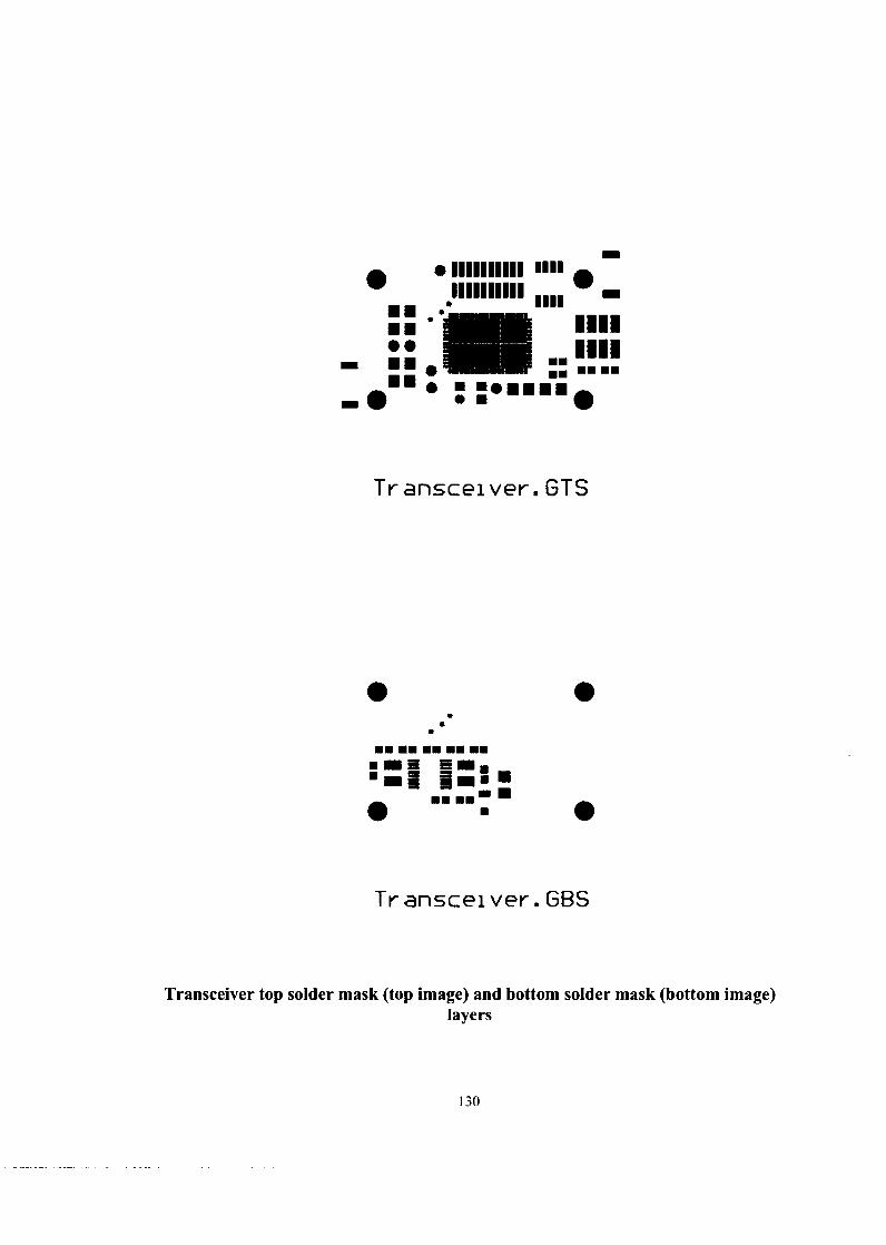
Transceiver . GTS
T r anscei ver . GBS
Transceiver top solder mask (top image) and bottom solder mask (bottom image) layers

REFERENCE LIST
1. W. E. Leigh and C. Burgess, "Distributed Intelligence: Trade-offs and Decisions for Computer Information Systems," South-Westem Publishing Co. 1987.
2. S. Androutsellis-Theotokis and D. Spinellis "A Survey of Peer-to-Peer Content Distribution Technologies," ACM Computing Surveys, Vol. 36, No. 4 December 2004, pp.335-371.
3. G. Coulouris, J. Dollimore, and T. Kindberg, "Distributed Systems: Concepts and Design " Pearson Education Ltd., 200 1.
4. S. Ovcharenko, Z. Alibhai, C. Ng, W.A. Gruver, and D. Sabaz, "Implementation of a Wireless Distributed Intelligent System" Proc. of the 2006 IEEE Workshop on Distributed Intelligent Systems, Prague, Czech Republic, June 2006.
5. G. Wong, "Hardware Design And Implementation For A Wireless Distributed Intelligent System Utilizing 802.11 ", M.Eng. Project Report, Simon Fraser University, Bumaby, BC, Canada, 2004.
6. A. K. Sharma, "Advanced Semiconductor Memories: Architectures, Designs, and Applications, " Wiley-Interscience, 2003.
7. P. Cappelletti et al., "Flash Memories, " Kluver Academic Publishers., 1999.
8. "Small Bock vs. Large Block NAND Devices: Technical Note, " Micron Technology, lnc., 2005.
9. J. LaRocca and R. LaRocca, "802.ll Demistzfied, " McGraw-Hill, 2002.
10. R. Roshan and J. Leary, "802.11 Wireless LAN Fundamentals, " Cisco Press., 2004.
1 1. B. Pattan, "Robust Modulation Methods and Smart Antennas in Wireless Communications, " Prentice Hall PTR , 2000.
12. Carl B.Dietrich, Jr., "Adaptive Arrays and Diversity Antenna Configurations for Handheld Wireless Communication Terminals", PhD Dissertation, http://scholar.lib.vt.edu/, February 2000.
13. "Connecting NAND Flash to the Intel PXA27x Processor Family"
14. "Stacked 1 Gb B-die Stacked SDRAM Specification" Rev. 1.1, Samsung, February 2005.
15. "Intel StrataFlash Embedded Memory (P30). Datasheet," November 2005.
16. "Intel PXA27x Processor Family: Design Guide," May 2005.
17. D. Brooks, "Signal Integrity And Printed Circuit Board Design, " Prentice Hall PTR, 2003.

18. S. H. Hall et al., "High Speed Digital System Design: A Handbook of Interconnect Theory and Design Practices, " John Wiley & Sons, 2000.
19. H. Johnson and M. Graham "High-speed Signal Propagation. Advanced Black Magic, " Prentice Hall PTR , 2003.