MKW2xD Data Sheet - NXP Semiconductors | Automotive, …€¦ · · 2016-11-2310.1...
78
MKW2xD Data Sheet Supports MKW24D512V, MKW22D512V, MKW21D512V, and MKW21D256V Products The MKW2xD is a low power, compact integrated device consisting of: • A high-performance 2.4 GHz IEEE 802.15.4 compliant radio transceiver • A powerful ARM Cortex-M4 MCU system with connectivity • Precision mixed signal analog peripherals The MKW2xD family of devices are used to easily enable connectivity based on the IEEE 802.15.4 Standard. Core Processor and Memories • 50 MHz Cortex-M4 CPU with DSP capabilities • Up to 512 KB of flash memory • Up to 64 KB of SRAM Typical Applications • Smart Energy 1.x • ZigBee Home Automation • ZigBee Healthcare • ZigBee RF4CE • ZigBee Light Link • Thread • Home Area Networks consisting of • Meters • Gateways • In-home displays • Connected appliances • Networked Building Control and Home Automations with • Lighting Control • HVAC • Security Peripherals • USB • Cryptographic Acceleration • 16-bit ADC • 12-bit DAC • Flexible timers Radio transceiver performance • Up to –102 dBm receiver sensitivity • +8 dBm maximum transmit output power • Up to 58 dBm channel rejection • Current consumption is minimized with peak transmit current of 17 mA at 0 dBm output power, and peak receive current of 15 mA in Low Power Preamble Search mode. Package and Operating Characteristics • Packaged in an 8 x 8 mm LGA with 56 contacts • Voltage range: 1.8 V to 3.6 V • Ambient temperature range: –40°C to 105°C MKW2xDxxxVHA5 64 LQFP 8.0x8.0x0.91 mm P 0.5 mm NXP Semiconductors MKW2xDxxx Data Sheet: Technical Data Rev. 2, 05/2016 NXP reserves the right to change the production detail specifications as may be required to permit improvements in the design of its products. © 2013–2016 NXP B.V.
Transcript of MKW2xD Data Sheet - NXP Semiconductors | Automotive, …€¦ · · 2016-11-2310.1...

MKW2xD Data SheetSupports MKW24D512V, MKW22D512V, MKW21D512V, andMKW21D256V Products
The MKW2xD is a low power, compact integrated deviceconsisting of:
• A high-performance 2.4 GHz IEEE 802.15.4 compliantradio transceiver
• A powerful ARM Cortex-M4 MCU system with connectivity• Precision mixed signal analog peripherals
The MKW2xD family of devices are used to easily enableconnectivity based on the IEEE 802.15.4 Standard.
Core Processor and Memories• 50 MHz Cortex-M4 CPU with DSP capabilities• Up to 512 KB of flash memory• Up to 64 KB of SRAM
Typical Applications• Smart Energy 1.x• ZigBee Home Automation• ZigBee Healthcare• ZigBee RF4CE• ZigBee Light Link• Thread• Home Area Networks consisting of
• Meters• Gateways• In-home displays• Connected appliances
• Networked Building Control and Home Automationswith
• Lighting Control• HVAC• Security
Peripherals• USB• Cryptographic Acceleration• 16-bit ADC• 12-bit DAC• Flexible timers
Radio transceiver performance• Up to –102 dBm receiver sensitivity• +8 dBm maximum transmit output power• Up to 58 dBm channel rejection• Current consumption is minimized with peak
transmit current of 17 mA at 0 dBm output power,and peak receive current of 15 mA in Low PowerPreamble Search mode.
Package and Operating Characteristics• Packaged in an 8 x 8 mm LGA with 56 contacts• Voltage range: 1.8 V to 3.6 V• Ambient temperature range: –40°C to 105°C
MKW2xDxxxVHA5
64 LQFP8.0x8.0x0.91 mm P 0.5 mm
NXP Semiconductors MKW2xDxxxData Sheet: Technical Data Rev. 2, 05/2016
NXP reserves the right to change the production detail specifications as may berequired to permit improvements in the design of its products. © 2013–2016 NXP B.V.

Ordering Information
Device
Operating TempRange
(TA)
PackageMemoryOptions
Description
MKW21D256VHA5(R) -40 to105°C
8x8 LGA (R: tapeand reel)
32 KBSRAM,256 KB
flash
Additional FlexMemory with up to 64 KB FlexNVM andup to 4 KB FlexRAM. No USB.
MKW21D512VHA5(R) -40 to105°C
8x8 LGA (R: tapeand reel)
64 KBSRAM,512 KB
flash
Supports higher memory option and additional GPIO.No USB. No FlexNVM or FlexRAM.
MKW22D512VHA5(R) -40 to105°C
8x8 LGA (R: tapeand reel)
64 KBSRAM,512 KB
flash
Supports full speed USB 2.0. No FlexNVM orFlexRAM.
MKW24D512VHA5(R) -40 to105°C
8x8 LGA (R: tapeand reel)
64 KBSRAM,512 KB
flash
Supports Smart Energy 2.0 and full-speed USB 2.0.No FlexNVM or FlexRAM.
Related Resources
Type Description Resource
SelectorGuide
The Kinetis MCUs Product Selector is a web-based tool that featuresinteractive application wizards and a dynamic product selector.
Product Selector
Fact Sheet The Fact Sheet gives overview of the product key features and its uses. KW2X Fact Sheet
ReferenceManual
The Reference Manual contains a comprehensive description of thestructure and function (operation) of a device.
MKW2xDRM1
Data Sheet The Data Sheet includes electrical characteristics and signalconnections.
This document.
Packagedrawing
Package dimensions are provided in package drawings. 98ASA00393D1
1. To find the associated resource, go to http://www.nxp.com and perform a search using this term.
2 MKW2xD Data Sheet, Rev. 2, 05/2016
NXP Semiconductors

Table of Contents
1 Features.............................................................................. 4
1.1 Block diagram............................................................ 4
1.2 Radio features............................................................4
1.3 Microcontroller features............................................. 5
2 Transceiver description....................................................... 8
2.1 Key specifications...................................................... 8
2.2 RF interface and usage..............................................9
2.2.1 Clock output feature.......................................9
2.3 Transceiver functions.................................................10
2.3.1 Receive.......................................................... 10
2.3.2 Transmit......................................................... 10
2.3.3 Clear channel assessment (CCA), energy
detection (ED), and link quality indicator
(LQI)...............................................................11
2.3.4 Packet processor........................................... 12
2.3.5 Packet buffering............................................. 13
2.4 Dual PAN ID...............................................................14
3 System and power management.........................................15
3.1 Modes of operation.................................................... 15
3.2 Power management...................................................15
4 Radio Peripherals................................................................16
4.1 Clock output (CLK_OUT)...........................................16
4.2 General-purpose input output (GPIO)........................16
4.3 Serial peripheral interface (SPI).................................18
4.3.1 Features.........................................................18
4.4 Antenna diversity....................................................... 19
4.5 RF Output Power Distribution.................................... 19
5 MKW2xD operating modes................................................. 20
5.1 Transceiver Transmit Current Distribution................. 21
6 MKW2xD electrical characteristics......................................22
6.1 Radio recommended operating conditions................ 22
6.2 Ratings.......................................................................23
6.2.1 Thermal handling ratings............................... 23
6.2.2 Moisture handling ratings...............................23
6.2.3 ESD handling ratings..................................... 23
6.2.4 Voltage and current operating ratings............24
7 MCU Electrical characteristics.............................................24
7.1 Maximum ratings........................................................24
7.2 AC electrical characteristics.......................................25
7.3 Nonswitching electrical specifications........................26
7.3.1 Voltage and current operating requirements..26
7.3.2 LVD and POR operating requirements.......... 27
7.3.3 Voltage and current operating behaviors....... 28
7.3.4 Power mode transition operating behaviors...28
7.3.5 Power consumption operating behaviors.......29
7.3.6 EMC radiated emissions operating
behaviors....................................................... 33
7.3.7 Designing with radiated emissions in mind.... 34
7.3.8 Capacitance attributes................................... 34
7.4 Switching specifications.............................................34
7.4.1 Device clock specifications............................ 34
7.4.2 General switching specifications....................35
7.5 Thermal specifications............................................... 36
7.5.1 Thermal operating requirements....................36
7.5.2 Thermal attributes.......................................... 36
7.6 Peripheral operating requirements and behaviors.....37
7.6.1 Core modules.................................................37
7.6.2 System modules............................................ 40
7.6.3 Clock modules............................................... 40
7.6.4 Memories and memory interfaces..................45
7.6.5 Security and integrity modules.......................49
7.6.6 Analog............................................................50
7.6.7 Timers............................................................ 57
7.6.8 Communication interfaces............................. 57
8 Transceiver Electrical Characteristics................................. 66
8.1 DC electrical characteristics.......................................66
8.2 AC electrical characteristics.......................................67
8.3 SPI timing: R_SSEL_B to R_SCLK........................... 68
8.4 SPI timing: R_SCLK to R_MOSI and R_MISO..........69
9 Crystal oscillator reference frequency.................................69
9.1 Crystal oscillator design considerations.....................69
9.2 Crystal requirements..................................................69
10 Pin diagrams and pin assignments..................................... 71
10.1 MKW21D256/MKW21D512 Pin Assignment............. 71
10.2 MKW22/24D512V Pin Assignment............................ 72
10.3 Pin assignments.........................................................72
11 Dimensions..........................................................................76
11.1 Obtaining package dimensions..................................76
12 Revision History.................................................................. 77
MKW2xD Data Sheet, Rev. 2, 05/2016 3
NXP Semiconductors
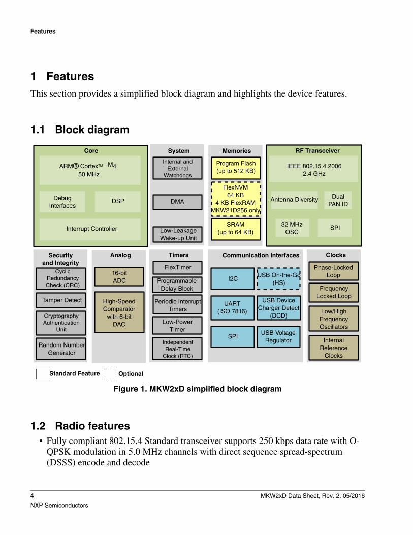
1 FeaturesThis section provides a simplified block diagram and highlights the device features.
1.1 Block diagram
Core
ARM® CortexTM –M4 50 MHz
Debug Interfaces
Interrupt Controller
DSP
System Memories RF Transceiver
Internal and External
Watchdogs
DMA
Low‐Leakage Wake‐up Unit
Program Flash (up to 512 KB)
FlexNVM 64 KB
4 KB FlexRAM MKW21D256 only
SRAM (up to 64 KB)
IEEE 802.15.4 2006 2.4 GHz
Antenna Diversity
32 MHz OSC
Dual PAN ID
SPI
Clocks
Phase‐Locked Loop
Communication Interfaces
I2CUSB On‐the‐Go
(HS)
Low/High Frequency Oscillators
UART (ISO 7816)
USB Device Charger Detect
(DCD)
Internal Reference
Clocks
SPIUSB Voltage
Regulator
Frequency Locked Loop
Timers
FlexTimer
Periodic Interrupt Timers
Low‐Power Timer
Programmable Delay Block
Independent Real‐Time
Clock (RTC)
Analog
16‐bit ADC
High‐Speed Comparator
with 6‐bit DAC
Security and Integrity
Cyclic Redundancy Check (CRC)
Cryptography Authentication
Unit
Random Number Generator
Tamper Detect
Standard Feature Optional
Figure 1. MKW2xD simplified block diagram
1.2 Radio features• Fully compliant 802.15.4 Standard transceiver supports 250 kbps data rate with O-
QPSK modulation in 5.0 MHz channels with direct sequence spread-spectrum(DSSS) encode and decode
Features
4 MKW2xD Data Sheet, Rev. 2, 05/2016
NXP Semiconductors
• Operates on one of 16 selectable channels in the 2.4 GHz frequency ISM band
• Programmable output power
• Supports 2.36 to 2.4 GHz Medical Band (MBAN) frequencies with samemodulation as IEEE 802.15.4
• Hardware acceleration for IEEE® 802.15.4 2006 packet processing
• Random number generator
• Support for dual PAN mode
• 32 MHz crystal reference oscillator with on board trim capability to supplementexternal load capacitors
• Programmable frequency clock output (CLK_OUT)
• Control port for Antenna Diversity mode
• Clocks
• 32 MHz crystal oscillator
• Internal 1 kHz low power oscillator
• DC to 32 MHz external square wave input clock
• Small RF footprint
• Differential input/output port used with external balun
• Integrated transmit/receive switch
• Supports single ended and antenna diversity options
• Low external components count
• Supports external PA and LNA
1.3 Microcontroller features• Core:
• ARM Cortex-M4 Core at 50 MHz (1.25 MIPS/MHz)
• Supports DSP instructions
Features
MKW2xD Data Sheet, Rev. 2, 05/2016 5
NXP Semiconductors

• Nested vectored interrupt controller (NVIC)
• Asynchronous wake-up interrupt controller (AWIC)
• Debug and trace capability
• 2-pin serial wire debug (SWD)
• IEEE 1149.1 Joint Test Action Group (JTAG)
• IEEE 1149.7 compact JTAG (cJTAG)
• Trace port interface unit (TPIU)
• Flash patch and breakpoint (FPB)
• Data watchpoint and trace (DWT)
• Instrumentation trace macrocell (ITM)
• Enhanced trace macrocell (ETM)
• System and power management:
• Software and hardware watchdog with external monitor pin
• DMA controller with 16 channels
• Low-leakage wake-up unit (LLWU)
• Power management controller with 10 different power modes
• Non-maskable interrupt (NMI)
• 128-bit unique identification (ID) number per chip
• Memories and memory interfaces:
• Up to 512 KB Program Flash
• Up to 64 KB of SRAM
• In MKW21D256, FlexMemory with up to 64 KB FlexNVM and up to 4 KBFlexRAM can be partitioned.
• EEPROM has endurance of 10 million cycles over full voltage and temperaturerange and read-while-write capability
• Flash security and protection features
• Serial flash programming interface (EzPort)
Features
6 MKW2xD Data Sheet, Rev. 2, 05/2016
NXP Semiconductors

• Clocks
• Multi-purpose clock generator
• PLL and FLL operation
• Internal reference clocks (32 kHz or 2 MHz)
• Three separate crystal oscillators
• 3 MHz to 32 MHz crystal oscillator for MCU
• 32 kHz to 40 kHz crystal oscillator for MCU or RTC
• 32 MHz crystal oscillator for Radio
• Internal 1 kHz low power oscillator
• DC to 50 MHz external square wave input clock
• Security and integrity
• Hardware CRC module to support fast cyclic redundancy checks
• Tamper detect and secure storage
• Hardware random-number generator
• Hardware encryption supporting DES, 3DES, AES, MD5, SHA-1, andSHA-256 algorithms
• 128-bit unique identification (ID) number per chip
• Analog
• 16-bit SAR ADC
• High-speed Analog comparator (CMP) with 6-bit DAC
• Timers
• Up to 12 channels; 7 channels support external connections; 5 channels areinternal only
• Carrier modulator timer (CMT)
• Programmable delay block (PDB)
• 1x4ch programmable interrupt timer (PIT)
Features
MKW2xD Data Sheet, Rev. 2, 05/2016 7
NXP Semiconductors

• Low-power timer (LPT)
• FlexTimers that support general-purpose PWM for motor control functions
• Communications
• One SPI
• Two I2C with SMBUS support
• Three UARTs (w/ ISO7816, IrDA, and hardware flow control)
• One USB On-The-Go Full Speed
• Human-machine interface
• GPIO with pin interrupt support, DMA request capability, digital glitch filter,and other pin control options
• Operating characteristics
• Voltage range 1.8 V - 3.6 V
• Flash memory programming down to 1.8 V
• Temperature range (TA) -40 to 105°C
Transceiver description
2.1 Key specifications
MKW2xD meets or exceeds all IEEE 802.15.4 performance specifications applicable to2.4 GHz ISM and MBAN (Medical Band Area Network) bands. Key specifications forMKW2xD are:
• ISM band:
• RF operating frequency: 2405 MHz to 2480 MHz (center frequency range)
• 5 MHz channel spacing
• MBAN band:
• RF operating frequency: 2360 MHz to 2400 MHz (center frequency range)
• MBAN channel page 9 is (2360 MHz-2390 MHz band)
2
Transceiver description
8 MKW2xD Data Sheet, Rev. 2, 05/2016
NXP Semiconductors

• Fc = 2363.0 + 1.0 * k in MHz for k = 0, 1, 2, ...26
• MBAN channel page 10 is (2390 MHz-2400 MHz band)
• Fc = 2390.0 + 1.0 * k in MHz for k = 0, 1, 2, ...8
• IEEE 802.15.4 Standard 2.4 GHz modulation scheme
• Chip rate: 2000 kbps
• Data rate: 250 kbps
• Symbol rate: 62.5 kbps
• Modulation: OQPSK
• Receiver sensitivity: -102 dBm, typical (@1% PER for 20 byte payload packet)
• Differential bidirectional RF input/output port with integrated transmit/receiveswitch
• Programmable output power from -35 dBm to +8 dBm.
2.2 RF interface and usage
The MKW2xD RF output ports are bidirectional (diplexed between receive/transmitmodes) and differential enabling interfaces with numerous off-chip devices such as abalun. When using a balun, this device provides an interface to directly connectbetween a single-ended antenna and the MKW2xD RF ports. In addition, MKW2xDprovides four output driver ports that can have both drive strength and slew rateconfigured to control external peripheral devices. These signals designated asANT_A, ANT_B, RX_SWITCH, and TX_SWITCH when enabled are switched viaan internal hardware state machine. These ports provide control features for peripheraldevices such as:
• Antenna diversity modules
• External PAs
• External LNAs
• T/R switches
Transceiver description
MKW2xD Data Sheet, Rev. 2, 05/2016 9
NXP Semiconductors

2.2.1 Clock output feature
The CLK_OUT digital output can be enabled to drive the system clock to the MCU.This provides a highly accurate clock source based on the transceiver referenceoscillator. The clock is programmable over a wide range of frequencies divided downfrom the reference 32 MHz (see Table 2). The CLK_OUT pin will be enabled uponPOR. The frequency CLK_OUT default to 4 MHz (32 MHz/8).
Transceiver functions
2.3.1 Receive
The receiver has the functionality to operate in either normal run state or low power runstate that can be considered as a partial power down mode. Low power run state cansave a considerable amount of current by duty-cycling some sections of the receiverlineup during preamble search and is referred to as Low Power Preamble Search mode(LPPS).
The radio receiver path is based upon a near zero IF (NZIF) architecture incorporatingfront end amplification, one mixed signal down conversion to IF that is programmablyfiltered, demodulated and digitally processed. The RF front end (FE) input port isdifferential that shares the same off chip matching network with the transmit path.
2.3.2 Transmit
MKW2xD transmits OQPSK modulation having power and channel selectionadjustment per user application. After the channel of operation is determined, coarseand fine tuning is executed within the Frac-N PLL to engage signal lock. After signallock is established, the modulated buffered signal is then routed to a multi-stageamplifier for transmission. The differential signals at the output of the PA (RFOUTP,RFOUTN) are converted as single ended (SE) signals with off chip components asrequired.
2.3
Transceiver functions
10 MKW2xD Data Sheet, Rev. 2, 05/2016
NXP Semiconductors

2.3.3 Clear channel assessment (CCA), energy detection (ED), andlink quality indicator (LQI)
The MKW2xD supports three clear channel assessment (CCA) modes of operationincluding energy detection (ED) and link quality indicator (LQI). Functionality foreach of these modes is as follows.
2.3.3.1 CCA mode 1
CCA mode 1 has two functions:
• To estimate the energy in the received baseband signal. This energy is estimatedbased on receiver signal strength indicator (RSSI).
• To determine whether the energy is greater than a set threshold.
The estimate of the energy can also be used as the Link Quality metric. In CCA Mode1, the MKW2xD must warm up from Idle to Receive mode where RSSI averagingtakes place.
2.3.3.2 CCA mode 2
CCA mode 2 detects whether there is any 802.15.4 signal transmitting in thefrequency band that an 802.15.4 transmitter intends to transmit. From the definition ofCCA mode 2 in the 802.15.4 standard, the requirement is to detect an 802.15.4complied signal. Whether the detected energy is strong or not is not important forCCA mode 2.
2.3.3.3 CCA mode 3
CCA mode 3 as defined by 802.15.4 standard is implemented using a logicalcombination of CCA mode 1 and CCA mode 2. Specifically, CCA mode 3 operates inone of two operating modes:
• CCA mode 3 is asserted if both CCA mode 1 and CCA mode 2 are asserted.
• CCA mode 3 is asserted if either CCA mode 1 or CCA mode 2 is asserted.
This mode setting is available through a programmable register.
Transceiver functions
MKW2xD Data Sheet, Rev. 2, 05/2016 11
NXP Semiconductors

2.3.3.4 Energy detection (ED)
Energy detection (ED) is based on receiver signal strength indicator (RSSI) andcorrelator output for the 802.15.4 standard. ED is an average value of signal strength.The magnitude from this measurement is calculated from the digital RSSI value that isaveraged over a 128 μs duration.
2.3.3.5 Link quality indicator (LQI)
Link quality indicator (LQI) is based on receiver signal strength indicator (RSSI) orcorrelator output for the 802.15.4 standard. In this mode, the RSSI measurement is doneduring normal packet reception. LQI computations for the MKW2xD are based oneither digital RSSI or correlator peak values. This setting is executed through a registerbit where the final LQI value is available 64 μs after preamble is detected. If acontinuous update of LQI based on RSSI throughout the packet is desired, it can be readin a separate 8-bit register by enabling continuous update in a register bit.
2.3.4 Packet processor
The MKW2xD packet processor performs sophisticated hardware filtering of theincoming received packet to determine if the packet is both PHY- and MAC-compliant,is addressed to this device, if the device is a PAN coordinator and whether a message ispending for the sending device. The packet processor greatly reduces the packetfiltering burden on software allowing it to tend to higher-layer tasks with a lowerlatency and smaller software footprint.
2.3.4.1 Features• Aggressive packet filtering to enable long, uninterrupted MCU sleep periods
• Fully compliant with both 2003 and 2006 versions of the 802.15.4 wirelessstandard
• Supports all frame types, including reserved types
• Supports all valid 802.15.4 frame lengths
• Enables auto-Tx acknowledge frames (no MCU intervention) by parsing of framecontrol field and sequence number
• Supports all source and destination address modes, and also PAN ID compression
• Supports broadcast address for PAN ID and short address mode
Transceiver functions
12 MKW2xD Data Sheet, Rev. 2, 05/2016
NXP Semiconductors

• Supports “promiscuous” mode, to receive all packets regardless of address- andrules-checking
• Allows frame type-specific filtering (e.g., reject all but beacon frames)
• Supports SLOTTED and non-SLOTTED modes
• Includes special filtering rules for PAN coordinator devices
• Enables minimum-turnaround Tx-acknowledge frames for data-polling requestsby automatically determining message-pending status
• Assists MCU in locating pending messages in its indirect queue for data-pollingend devices
• Makes available to MCU detailed status of frames that fail address- or rules-checking.
• Supports Dual PAN mode, allowing the device to exist on 2 PAN'ssimultaneously
• Supports 2 IEEE addresses for the device
• Supports active promiscuous mode
2.3.5 Packet buffering
The packet buffer is a 128-byte random access memory (RAM) dedicated to thestorage of 802.15.4 packet contents for both TX and RX sequences. For TXsequences, software stores the contents of the packet buffer starting with the framelength byte at packet buffer address 0 followed by the packet contents at thesubsequent packet buffer addresses. For RX sequences the incoming packet's framelength is stored in a register external to the packet buffer. Software will read thisregister to determine the number of bytes of packet buffer to read. This facilitatesDMA transfer through the SPI. For receive packets, an LQI byte is stored at the byteimmediately following the last byte of the packet (frame length +1). Usage of thepacket buffer for RX and TX sequences is on a time-shared basis; receive packet datawill overwrite the contents of the packet buffer. Software can inhibit receive-packetoverwriting of the packet buffer contents by setting the PB_PROTECT bit. This willblock RX packet overwriting, but will not inhibit TX content loading of the packetbuffer via the SPI.
Transceiver functions
MKW2xD Data Sheet, Rev. 2, 05/2016 13
NXP Semiconductors

2.3.5.1 Features• 128 byte buffer stores maximum length 802.15.4 packets
• Same buffer serves both TX and RX sequences
• The entire Packet Buffer can be uploaded or downloaded in a single SPI burst.
• Automatic address auto-incrementing for burst accesses
• Single-byte access mode supported.
• Entire packet buffer can be accessed in hibernate mode
• Under-run error interrupt supported
2.4 Dual PAN ID
In the past, radio transceivers designed for IEEE 802.15.4 applications allowed a deviceto associate to one and only one PAN (Personal Area Network) at any given time. TheMKW2xD represents a high-performance SiP that includes hardware support for adevice to reside in two networks simultaneously. In optional Dual PAN mode, thedevice alternates between the two (2) PANs under hardware or software control.Hardware support for Dual PAN operation consists of two (2) sets of PAN and IEEEaddresses for the device, two (2) different channels (one for each PAN) and aprogrammable timer to automatically switch PANs (including on-the-fly channelchanging) without software intervention. There are control bits to configure and enableDual PAN mode, and read only bits to monitor status in Dual PAN mode. A device canbe configured to be a PAN coordinator on either network, both networks or neither.
For the purpose of defining PAN in the context of Dual PAN mode, two (2) sets ofnetwork parameters are maintained; PAN0 and PAN1. PAN0 and PAN1 will be used torefer to the two (2) PANs where each parameter set uniquely identifies a PAN for DualPAN mode. These parameters are described in Table 1.
Table 1. PAN0 and PAN1 descriptions
PAN0 PAN1
Channel0 (PHY_INT0, PHY_FRAC0) Channel1 (PHY_INT1, PHY_FRAC1)
MacPANID0 (16-bit register) MacPANID1 (16-bit register)
MacShortAddrs0 (16-bit register) MacShortAddrs1 (16-bit register)
MacLongAddrs0 (64-bit registers) MacLongAddrs1 (64-bit registers)
PANCORDNTR0 (1-bit register) PANCORDNTR1 (1-bit register)
Transceiver functions
14 MKW2xD Data Sheet, Rev. 2, 05/2016
NXP Semiconductors

During device initialization if Dual PAN mode is used, software will program bothparameter sets to configure the hardware for operation on two (2) networks.
3 System and power managementThe MKW2xD is a low power device that also supports extensive system control andpower management modes to maximize battery life and provide system protection.
3.1 Modes of operation
The transceiver modes of operation include:
• Idle mode
• Doze mode
• Low power (LP) / hibernate mode
• Reset / powerdown mode
• Run mode
3.2 Power management
The MKW2xD power management is controlled through programming the modes ofoperation. Different modes allow for different levels of power-down and RUNoperation. For the receiver, programmable power modes available are:
• Preamble search
• Preamble search sniff
• Low Power Preamble Search (LPPS)
• Fast Antenna Diversity (FAD) Preamble search
• Packet decoding
System and power management
MKW2xD Data Sheet, Rev. 2, 05/2016 15
NXP Semiconductors

4 Radio PeripheralsThe MKW2xD provides a set of I/O pins useful for suppling a system clock to theMCU, controlling external RF modules/circuitry, and GPIO.
4.1 Clock output (CLK_OUT)
MKW2xD integrates a programmable clock to source numerous frequencies forconnection with various MCUs. Package pin 39 can be used to provide this clock sourceas required allowing the user to make adjustments per their application requirement.
The transceiver CLK_OUT pin is internally connected to the MCU EXTAL pin so thatno external connection is needed to drive the MCU clock.
Care must be taken that the clock output signal does not interfere with the referenceoscillator or the radio. Additional functionality this feature supports is:
• XTAL domain can be completely gated off (hibernate mode)
• SPI communication allowed in hibernate
Table 2. CLK_OUT
CLK_OUT_DIV [2:0] CLK_OUT frequency
0 32 MHz1
1 16 MHz1
2 8 MHz1
3 4 MHz
4 2 MHz
5 1 MHz
6 62.5 kHz
7 32.786 kHz
1. May require high drive strength for proper signal integrity.
There is an enable/disable bit for CLK_OUT. When disabling, the clock output willoptionally continue to run for 128 clock cycles after disablement. There is also be one(1) bit available to adjust the CLK_OUT I/O pad drive strength.
Radio Peripherals
16 MKW2xD Data Sheet, Rev. 2, 05/2016
NXP Semiconductors

4.2 General-purpose input output (GPIO)
In addition to the MCU supported GPIOs, the radio supports 2 GPIO pins. All I/Opins will have the same supply voltage and depending on the supply, can vary from1.8 V up to 3.6 V. When the pin is configured as a general-purpose output or forperipheral use, there will be specific settings required per use case. Pin configurationwill be executed by software to adjust input/output direction and drive strength,capability. When the pin is configured as a general-purpose input or for peripheraluse, software (see Table 3) can enable a pull-up or pull-down device. Immediatelyafter reset, all pins are configured as high-impedance general-purpose inputs withinternal pull-up devices enabled.
Features for these pins include:
• Programmable output drive strength
• Programmable output slew rate
• Hi-Z mode
• Programmable as outputs or inputs (default)
Table 3. Pin configuration summary
Pin function configuration DetailsTolerance
UnitsMin. Typ. Max.
I/O buffer full drive mode1 Source or sink — ±10 — mA
I/O buffer partial drive mode1 Source or sink — ±2 — mA
I/O buffer high impedance2 Off state — — 10 nA
No slew, full drive Rise and fall time3 2 4 6 ns
No slew, partial drive Rise and fall time 2 4 6 ns
Slew, full drive Rise and fall time 6 12 24 ns
Slew, partial drive Rise and fall time 6 12 24 ns
Propagation delay4, no slew Full drive5 — — 11 ns
Propagation delay, no slew Partial drive6 — — 11 ns
Propagation delay, slew Full drive — — 50 ns
Propagation delay, slew Partial drive — — 50 ns
1. For this drive condition, the output voltage will not deviate more than 0.5 V from the rail reference VOH or VOL.2. Leakage current applies for the full range of possible input voltage conditions.3. Rise and fall time values in reference to 20% and 80%4. Propagation Delay measured from/to 50% voltage point.5. Full drive values provided are in reference to a 75 pF load.6. Partial drive values provided are in reference to a 15 pF load.
Radio Peripherals
MKW2xD Data Sheet, Rev. 2, 05/2016 17
NXP Semiconductors

4.3 Serial peripheral interface (SPI)
The MKW2xD SiP uses a SPI interface allowing the MCU to communicate with theradio's register set and packet buffer. The SPI is a slave-only interface; the MCU mustdrive R_SSEL_B, R_SCLK and R_MOSI. Write and read access to both direct andindirect registers is supported, and transfer length can be single-byte or bursts ofunlimited length. Write and read access to the Packet buffer can also be single-byte or aburst mode of unlimited length.
The SPI interface is asynchronous to the rest of the IC. No relationship betweenR_SCLK and MKW2xD's internal oscillator is assumed. And no relationship betweenR_SCLK and the CLK_OUT pin is assumed. All synchronization of the SPI interface tothe IC takes place inside the SPI module. SPI synchronization takes place in bothdirections; register writes and register reads. The SPI is capable of operation in allpower modes, except Reset. Operation in hibernate mode allows most transceiverregisters and the complete packet buffer to be accessed in the lowest-power operatingstate enabling minimal power consumption, especially during the register-initializationphase of the radio.
The SPI design features a compact, single-byte control word, reducing SPI accesslatency to a minimum. Most SPI access types require only a single-byte control word,with the address embedded in the control word. During control word transfer (the firstbyte of any SPI access), the contents of the IRQSTS1 register (MKW2xD radio'shighest-priority status register) are always shifted out so that the MCU gets access toIRQSTS1, with the minimum possible latency, on every SPI access.
4.3.1 Features• 4-wire industry standard interface, supported by all MCUs
• SPI R_SCLK maximum frequency 16 MHz (for SPI write accesses)
• SPI R_SCLK maximum frequency 9 MHz (for SPI read accesses)
• Write and read access to all radio registers (direct and indirect)
• Write and read access to packet buffer
• SPI accesses can be single-byte or burst
• Automatic address auto-incrementing for burst accesses
Radio Peripherals
18 MKW2xD Data Sheet, Rev. 2, 05/2016
NXP Semiconductors

• The entire packet buffer can be uploaded or downloaded in a single SPI burst
• Entire packet buffer and most registers can be accessed in hibernate mode
• Built-in synchronization inside the SPI module to/from the rest of the radio
4.4 Antenna diversity
To improve the reliability of RF connectivity to long range applications, the antennadiversity feature is supported without using the MCU through use of four dedicatedcontrol pins (package pins 44, 45, 46, and 47).
Fast antenna diversity (FAD) mode supports this radio feature and, when enabled, willallow the choice of selection between two antennas during the preamble phase. Bycontinually monitoring the received signal, the FAD block will select the first antennaof which the received signal has a correlation factor above a predefined progammablethreshold. The FAD accomplishes the antenna selection by sequentially switchingbetween the two antennas testing for the presence of suitably strong s0 symbol wherethe first antenna to reach this condition is then selected for the reception of the packet.
The antenna's are monitored for a period of 28 μs each. The antenna switching iscontinued until 1.5 valid s0 symbols are detected. The demodulator then continueswith normal preamble search before declaring “Preamble Detect”.
4.5 RF Output Power Distribution
The following figure shows the linear region of the output and the typical powerdistribution of the radio as a function of PA_PWR [4:0] range. The PA_PWR [4:0] isthe lower 5 bits of the PA_PWR 0x23 direct register and has a usable range of 3 to 31decimal.
Radio Peripherals
MKW2xD Data Sheet, Rev. 2, 05/2016 19
NXP Semiconductors

Figure 2. MKW2xD transmit power vs. PA_PWR step
5 MKW2xD operating modesFor the discussion of this topic, the primary radio and MCU operating modes arecombined so that overall power consumption can then be derived. Depending on thestop requirements of the user application, a variety of stop modes are available thatprovide state retention, partial power down or full power down of certain logic and/ormemory. I/O states are held in all modes of operation. Both the radio and MCU's powermodes are described as follows.
The radio has 6 primary operating modes:
• Reset / power down
• Low power (LP) / hibernate
• Doze (low power with reference oscillator active)
MKW2xD operating modes
20 MKW2xD Data Sheet, Rev. 2, 05/2016
NXP Semiconductors

• Idle
• Receive
• Transmit
Table 4 lists and describes the transceivers power modes and consumption.
Table 4. Transceiver Power Modes
Mode DefinitionCurrent
consumption1
Reset /powerdow
n
All IC functions off, leakage only. RST asserted. < 100 nA
Lowpower /
hibernate
Crystal reference oscillator off. (SPI is functional.) < 1 μA
Doze2 Crystal reference oscillator on but CLK_OUT output available only if selected. 500 μA3
(no CLK_OUT)
Idle Crystal reference oscillator on with CLK_OUT output available only if selected. 700 μA3
(no CLK_OUT)
Receive Crystal reference oscillator on. Receiver on. < 19.5 mA 4
15 mA, LPPSmode
Transmit Crystal reference oscillator on. Transmitter on. < 18 mA 5
1. Conditions: VBAT and VBAT_2 = 2.7 V, nominal process @ 25°C2. While in Doze mode, 4 MHz max frequency can be selected for CLK_OUT.3. Typical4. Signal sensitivity = -102 dBm5. RF output = 0 dBm
The MCU has a variety of operating modes. For each run mode there is acorresponding wait and stop mode. Wait modes are similar to ARM sleep modes. Stopmodes (VLPS, STOP) are similar to ARM sleep deep mode. The very low power run(VLPR) operating mode can drastically reduce runtime power when the maximum busfrequency is not required to handle the application needs.
The three primary modes of operation are run, wait and stop. The WFI instructioninvokes both wait and stop modes for the chip. The primary modes are augmented in anumber of ways to provide lower power based on application needs.
MKW2xD operating modes
MKW2xD Data Sheet, Rev. 2, 05/2016 21
NXP Semiconductors

5.1 Transceiver Transmit Current Distribution
The following figure shows the relation between the transmit power generated by theradio and its current consumption.
Figure 3. MKW2xD transmit power vs transmit current (Radio Only)
MKW2xD electrical characteristics
6.1 Radio recommended operating conditionsTable 5. Recommended operating conditions
Characteristic Symbol Min Typ Max Unit
Power Supply Voltage (VBAT = VDDINT) VBAT, VDDINT 1.8 2.7 3.6 Vdc
Input Frequency fin 2.360 — 2.480 GHz
Ambient Temperature Range TA -40 25 105 °C
Table continues on the next page...
6
MKW2xD electrical characteristics
22 MKW2xD Data Sheet, Rev. 2, 05/2016
NXP Semiconductors

Table 5. Recommended operating conditions (continued)
Characteristic Symbol Min Typ Max Unit
Logic Input Voltage Low VIL 0 — 30%VDDINT
V
Logic Input Voltage High VIH 70%VDDINT
— VDDINT V
SPI Clock Rate fSPI — — 16.0 MHz
RF Input Power Pmax — — 10 dBm
Crystal Reference Oscillator Frequency (±40 ppm overoperating conditions to meet the 802.15.4 Standard.)
fref 32 MHz only
Ratings
6.2.1 Thermal handling ratings
Symbol Description Min. Max. Unit Notes
TSTG Storage temperature –55 150 °C 1
TSDR Solder temperature, lead-free — 260 °C 2
1. Determined according to JEDEC Standard JESD22-A103, High Temperature Storage Life.2. Determined according to IPC/JEDEC Standard J-STD-020, Moisture/Reflow Sensitivity Classification for Nonhermetic
Solid State Surface Mount Devices.
6.2.2 Moisture handling ratings
Symbol Description Min. Max. Unit Notes
MSL Moisture sensitivity level — 3 — 1
1. Determined according to IPC/JEDEC Standard J-STD-020, Moisture/Reflow Sensitivity Classification for NonhermeticSolid State Surface Mount Devices.
6.2.3 ESD handling ratings
Symbol Description Min. Max. Unit Notes
VHBM Electrostatic discharge voltage, human body model -2000 +2000 V 1
VCDM Electrostatic discharge voltage, charged-devicemodel
-500 +500 V 2
Table continues on the next page...
6.2
Ratings
MKW2xD Data Sheet, Rev. 2, 05/2016 23
NXP Semiconductors
Symbol Description Min. Max. Unit Notes
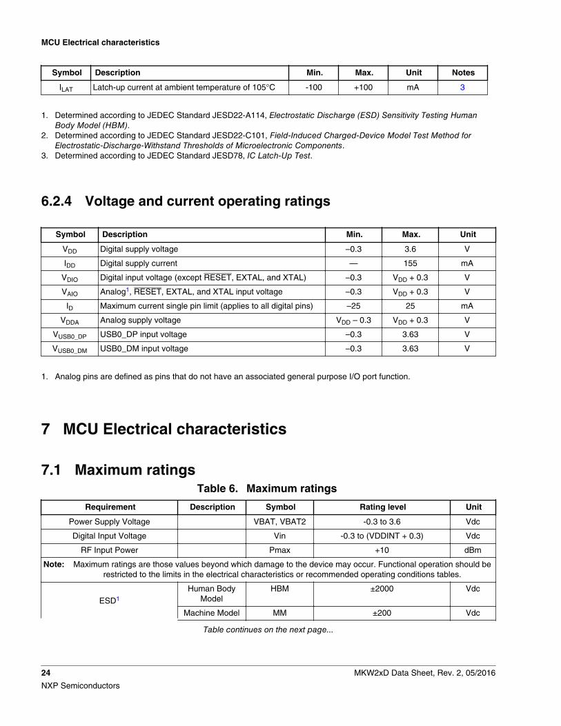
ILAT Latch-up current at ambient temperature of 105°C -100 +100 mA 3
1. Determined according to JEDEC Standard JESD22-A114, Electrostatic Discharge (ESD) Sensitivity Testing HumanBody Model (HBM).
2. Determined according to JEDEC Standard JESD22-C101, Field-Induced Charged-Device Model Test Method forElectrostatic-Discharge-Withstand Thresholds of Microelectronic Components.
3. Determined according to JEDEC Standard JESD78, IC Latch-Up Test.
6.2.4 Voltage and current operating ratings
Symbol Description Min. Max. Unit
VDD Digital supply voltage –0.3 3.6 V
IDD Digital supply current — 155 mA
VDIO Digital input voltage (except RESET, EXTAL, and XTAL) –0.3 VDD + 0.3 V
VAIO Analog1, RESET, EXTAL, and XTAL input voltage –0.3 VDD + 0.3 V
ID Maximum current single pin limit (applies to all digital pins) –25 25 mA
VDDA Analog supply voltage VDD – 0.3 VDD + 0.3 V
VUSB0_DP USB0_DP input voltage –0.3 3.63 V
VUSB0_DM USB0_DM input voltage –0.3 3.63 V
1. Analog pins are defined as pins that do not have an associated general purpose I/O port function.
MCU Electrical characteristics
7.1 Maximum ratingsTable 6. Maximum ratings
Requirement Description Symbol Rating level Unit
Power Supply Voltage VBAT, VBAT2 -0.3 to 3.6 Vdc
Digital Input Voltage Vin -0.3 to (VDDINT + 0.3) Vdc
RF Input Power Pmax +10 dBm
Note: Maximum ratings are those values beyond which damage to the device may occur. Functional operation should berestricted to the limits in the electrical characteristics or recommended operating conditions tables.
ESD1
Human BodyModel
HBM ±2000 Vdc
Machine Model MM ±200 Vdc
Table continues on the next page...
7
MCU Electrical characteristics
24 MKW2xD Data Sheet, Rev. 2, 05/2016
NXP Semiconductors

Table 6. Maximum ratings (continued)
Requirement Description Symbol Rating level Unit
Charged DeviceModel
CDM ±750 Vdc
EMC2
Power Electro-Static
Discharge /Direct Contact
PESD
No damage / latch up to ±4000
VdcNo soft failure / reset to ±1000
Power Electro-Static
Discharge /Indirect Contact
No damage / latch up to ±6000
VdcNo soft failure / reset to ±1000
Langer IC / EFT /P201 EFT (Electro
Magnetic FastTransient)
No damage / latch up to ±5Vdc
No soft failure / reset to ±5
Langer IC / EFT /P201
No damage / latch up to ±300Vdc
No soft failure / reset to ±150
Junction Temperature TJ +125 °C
Storage Temperature Range Tstg -65 to +165 °C
1. Electrostatic discharge on all device pads meet this requirement2. Electromagnetic compatibility for this product is low stress rating level
Note
Maximum ratings are those values beyond which damage tothe device may occur. Functional operation should berestricted to the limits in the electrical characteristics orrecommended operating conditions tables.
7.2 AC electrical characteristics
Unless otherwise specified, propagation delays are measured from the 50% to the 50%point, and rise and fall times are measured at the 20% and 80% points, as shown in thefollowing figure.
MCU Electrical characteristics
MKW2xD Data Sheet, Rev. 2, 05/2016 25
NXP Semiconductors

80%
20%50%
VIL
Input Signal
VIH
Fall Time
HighLow
Rise Time
Midpoint1
The midpoint is VIL + (VIH - VIL) / 2
Figure 4. Input signal measurement reference
7.3 Nonswitching electrical specifications
7.3.1 Voltage and current operating requirementsTable 7. Voltage and current operating requirements
Symbol Description Min. Max. Unit Notes
VDD Supply voltage 1.8 3.6 V
VDDA Analog supply voltage 1.8 3.6 V
VDD – VDDA VDD-to-VDDA differential voltage –0.1 0.1 V
VSS – VSSA VSS-to-VSSA differential voltage –0.1 0.1 V
VBAT RTC battery supply voltage 1.8 3.6 V
VIH Input high voltage
• 2.7 V ≤ VDD ≤ 3.6 V
• 1.7 V ≤ VDD ≤ 2.7 V
0.7 × VDD
0.75 × VDD
—
—
V
V
VIL Input low voltage
• 2.7 V ≤ VDD ≤ 3.6 V
• 1.7 V ≤ VDD ≤ 2.7 V
—
—
0.35 × VDD
0.3 × VDD
V
V
VHYS Input hysteresis 0.06 × VDD — V
IICIO I/O pin DC injection current — single pin
• VIN < VSS-0.3V (Negative current injection)
• VIN > VDD+0.3V (Positive current injection)
-3
—
—
+3
mA
1
IICcont Contiguous pin DC injection current —regional limit,includes sum of negative injection currents or sum ofpositive injection currents of 16 contiguous pins
• Negative current injection
• Positive current injection
-25
—
—
+25
mA
Table continues on the next page...
MCU Electrical characteristics
26 MKW2xD Data Sheet, Rev. 2, 05/2016
NXP Semiconductors

Table 7. Voltage and current operating requirements (continued)
Symbol Description Min. Max. Unit Notes
VRAM VDD voltage required to retain RAM 1.2 — V
VRFVBAT VBAT voltage required to retain the VBAT register file VPOR_VBAT — V
1. All analog pins are internally clamped to VSS and VDD through ESD protection diodes. If VIN is less than VAIO_MIN orgreater than VAIO_MAX, a current limiting resistor is required. The negative DC injection current limiting resistor iscalculated as R=(VAIO_MIN-VIN)/|IICAIO|. The positive injection current limiting resistor is calculated as R=(VIN-VAIO_MAX)/|IICAIO|. Select the larger of these two calculated resistances if the pin is exposed to positive and negativeinjection currents.
7.3.2 LVD and POR operating requirementsTable 8. VDD supply LVD and POR operating requirements
Symbol Description Min. Typ. Max. Unit Notes
VPOR Falling VDD POR detect voltage 0.8 1.1 1.5 V
VLVDH Falling low-voltage detect threshold — highrange (LVDV=01)
2.48 2.56 2.64 V
VLVW1H
VLVW2H
VLVW3H
VLVW4H
Low-voltage warning thresholds — high range
• Level 1 falling (LVWV=00)
• Level 2 falling (LVWV=01)
• Level 3 falling (LVWV=10)
• Level 4 falling (LVWV=11)
2.62
2.72
2.82
2.92
2.70
2.80
2.90
3.00
2.78
2.88
2.98
3.08
V
V
V
V
1
VHYSH Low-voltage inhibit reset/recover hysteresis —high range
— 80 — mV
VLVDL Falling low-voltage detect threshold — lowrange (LVDV=00)
1.54 1.60 1.66 V
VLVW1L
VLVW2L
VLVW3L
VLVW4L
Low-voltage warning thresholds — low range
• Level 1 falling (LVWV=00)
• Level 2 falling (LVWV=01)
• Level 3 falling (LVWV=10)
• Level 4 falling (LVWV=11)
1.74
1.84
1.94
2.04
1.80
1.90
2.00
2.10
1.86
1.96
2.06
2.16
V
V
V
V
1
VHYSL Low-voltage inhibit reset/recover hysteresis —low range
— 60 — mV
VBG Bandgap voltage reference 0.97 1.00 1.03 V
tLPO Internal low power oscillator period — factorytrimmed
900 1000 1100 μs
MCU Electrical characteristics
MKW2xD Data Sheet, Rev. 2, 05/2016 27
NXP Semiconductors

1. Rising threshold is the sum of falling threshold and hysteresis voltage
Table 9. VBAT power operating requirements
Symbol Description Min. Typ. Max. Unit Notes
VPOR_VBAT Falling VBAT supply POR detect voltage 0.8 1.1 1.5 V
7.3.3 Voltage and current operating behaviorsTable 10. Voltage and current operating behaviors
Symbol Description Min. Max. Unit Notes
VOH Output high voltage — high drive strength
• 2.7 V ≤ VDD ≤ 3.6 V, IOH = - 9 mA
• 1.71 V ≤ VDD ≤ 2.7 V, IOH = -3 mA
VDD – 0.5
VDD – 0.5
—
—
V
V
Output high voltage — low drive strength
• 2.7 V ≤ VDD ≤ 3.6 V, IOH = -2 mA
• 1.71 V ≤ VDD ≤ 2.7 V, IOH = -0.6 mA
VDD – 0.5
VDD – 0.5
—
—
V
V
IOHT Output high current total for all ports — 100 mA
VOL Output low voltage — high drive strength
• 2.7 V ≤ VDD ≤ 3.6 V, IOL = 9 mA
• 1.71 V ≤ VDD ≤ 2.7 V, IOL = 3 mA
—
—
0.5
0.5
V
V
Output low voltage — low drive strength
• 2.7 V ≤ VDD ≤ 3.6 V, IOL = 2 mA
• 1.71 V ≤ VDD ≤ 2.7 V, IOL = 0.6 mA
—
—
0.5
0.5
V
V
IOLT Output low current total for all ports — 100 mA
IIN Input leakage current (per pin)
• @ full temperature range
• @ 25 °C
—
—
1.0
0.1
μA
μA
1
IOZ Hi-Z (off-state) leakage current (per pin) — 1 μA
IOZ Total Hi-Z (off-state) leakage current (all input pins) — 4 μA
RPU Internal pullup resistors 22 50 kΩ 2
RPD Internal pulldown resistors 22 50 kΩ 3
1. Tested by ganged leakage method2. Measured at Vinput = VSS3. Measured at Vinput = VDD
MCU Electrical characteristics
28 MKW2xD Data Sheet, Rev. 2, 05/2016
NXP Semiconductors

7.3.4 Power mode transition operating behaviors
All specifications except tPOR, and VLLSx→RUN recovery times in the followingtable assume this clock configuration:
• CPU and system clocks = 50 MHz• Bus clock = 50 MHz• Flash clock = 25 MHz• MCG mode: FEI
Table 11. Power mode transition operating behaviors
Symbol Description Min. Max. Unit Notes
tPOR After a POR event, amount of time from the pointVDD reaches 1.71 V to execution of the firstinstruction across the operating temperature rangeof the chip.
• 1.71 V/(VDD slew rate) ≤ 300 μs
• 1.71 V/(VDD slew rate) > 300 μs
—
—
300
1.7 V / (VDDslew rate)
μs 1
• VLLS1 → RUN— 150 μs
• VLLS2 → RUN— 79 μs
• VLLS3 → RUN— 79 μs
• LLS → RUN— 6 μs
• VLPS → RUN— 5.2 μs
• STOP → RUN— 5.2 μs
1. Normal boot (FTFL_OPT[LPBOOT]=1)
7.3.5 Power consumption operating behaviorsTable 12. Power consumption operating behaviors
Symbol Description Min. Typ. Max. Unit Notes
IDDA Analog supply current — — See note mA 1
IDD_RUN Run mode current — all peripheral clocksdisabled, code executing from flash
• @ 1.8 V
• @ 3.0 V
—
—
12.98
12.93
14
13.8
mA
mA
2
Table continues on the next page...
MCU Electrical characteristics
MKW2xD Data Sheet, Rev. 2, 05/2016 29
NXP Semiconductors

Table 12. Power consumption operating behaviors (continued)
Symbol Description Min. Typ. Max. Unit Notes
IDD_RUN Run mode current — all peripheral clocksenabled, code executing from flash
• @ 1.8 V
• @ 3.0 V
• @ 25°C
• @ 125°C
—
—
—
17.04
17.01
19.8
19.3
18.9
21.3
mA
mA
mA
3, 4
IDD_WAIT Wait mode high frequency current at 3.0 V —all peripheral clocks disabled
— 7.95 9.5 mA 2
IDD_WAIT Wait mode reduced frequency current at 3.0 V— all peripheral clocks disabled
— 5.88 7.4 mA 5
IDD_STOP Stop mode current at 3.0 V• @ –40 to 25°C• @ 50°C• @ 70°C• @ 105°C
—320
360
410
610
436
489
620
1100
μA
IDD_VLPR Very-low-power run mode current at 3.0 V —all peripheral clocks disabled
— 754 — μA 6
IDD_VLPR Very-low-power run mode current at 3.0 V —all peripheral clocks enabled
— 1.1 — mA 7
IDD_VLPW Very-low-power wait mode current at 3.0 V — 437 — μA 8
IDD_VLPS Very-low-power stop mode current at 3.0 V• @ –40 to 25°C• @ 50°C• @ 70°C• @ 105°C
—7.33
14
28
110
24.2
32
48
280
μA
IDD_LLS Low leakage stop mode current at 3.0 V• @ –40 to 25°C• @ 50°C• @ 70°C• @ 105°C
—3.14
6.48
13.85
55.53
4.8
28.3
44.6
71.3
μA
IDD_VLLS3 Very low-leakage stop mode 3 current at 3.0 V
• @ –40 to 25°C• @ 50°C• @ 70°C• @ 105°C
— 2.19
4.35
8.92
35.33
3.4
4.35
24.6
45.3
μA
IDD_VLLS2 Very low-leakage stop mode 2 current at 3.0 V• @ –40 to 25°C• @ 50°C• @ 70°C• @ 105°C
—1.77
2.81
5.20
19.88
3.1
13.8
22.3
34.2
μA
IDD_VLLS1 Very low-leakage stop mode 1 current at 3.0 V• @ –40 to 25°C
—1.03 1.8
μA
Table continues on the next page...
MCU Electrical characteristics
30 MKW2xD Data Sheet, Rev. 2, 05/2016
NXP Semiconductors
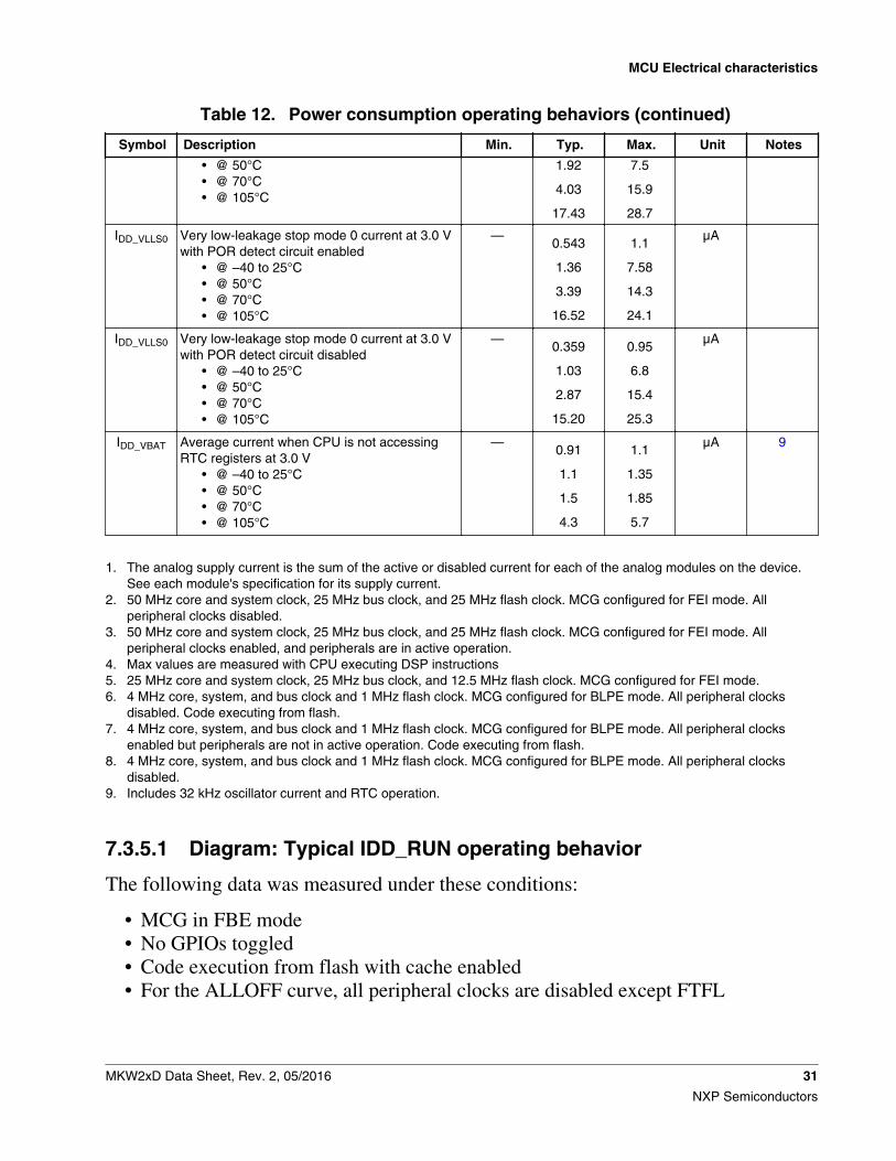
Table 12. Power consumption operating behaviors (continued)
Symbol Description Min. Typ. Max. Unit Notes
• @ 50°C• @ 70°C• @ 105°C
1.92
4.03
17.43
7.5
15.9
28.7
IDD_VLLS0 Very low-leakage stop mode 0 current at 3.0 Vwith POR detect circuit enabled
• @ –40 to 25°C• @ 50°C• @ 70°C• @ 105°C
—0.543
1.36
3.39
16.52
1.1
7.58
14.3
24.1
μA
IDD_VLLS0 Very low-leakage stop mode 0 current at 3.0 Vwith POR detect circuit disabled
• @ –40 to 25°C• @ 50°C• @ 70°C• @ 105°C
—0.359
1.03
2.87
15.20
0.95
6.8
15.4
25.3
μA
IDD_VBAT Average current when CPU is not accessingRTC registers at 3.0 V
• @ –40 to 25°C• @ 50°C• @ 70°C• @ 105°C
—0.91
1.1
1.5
4.3
1.1
1.35
1.85
5.7
μA 9
1. The analog supply current is the sum of the active or disabled current for each of the analog modules on the device.See each module's specification for its supply current.
2. 50 MHz core and system clock, 25 MHz bus clock, and 25 MHz flash clock. MCG configured for FEI mode. Allperipheral clocks disabled.
3. 50 MHz core and system clock, 25 MHz bus clock, and 25 MHz flash clock. MCG configured for FEI mode. Allperipheral clocks enabled, and peripherals are in active operation.
4. Max values are measured with CPU executing DSP instructions5. 25 MHz core and system clock, 25 MHz bus clock, and 12.5 MHz flash clock. MCG configured for FEI mode.6. 4 MHz core, system, and bus clock and 1 MHz flash clock. MCG configured for BLPE mode. All peripheral clocks
disabled. Code executing from flash.7. 4 MHz core, system, and bus clock and 1 MHz flash clock. MCG configured for BLPE mode. All peripheral clocks
enabled but peripherals are not in active operation. Code executing from flash.8. 4 MHz core, system, and bus clock and 1 MHz flash clock. MCG configured for BLPE mode. All peripheral clocks
disabled.9. Includes 32 kHz oscillator current and RTC operation.
7.3.5.1 Diagram: Typical IDD_RUN operating behavior
The following data was measured under these conditions:
• MCG in FBE mode• No GPIOs toggled• Code execution from flash with cache enabled• For the ALLOFF curve, all peripheral clocks are disabled except FTFL
MCU Electrical characteristics
MKW2xD Data Sheet, Rev. 2, 05/2016 31
NXP Semiconductors

Figure 5. Run mode supply current vs. core frequency
MCU Electrical characteristics
32 MKW2xD Data Sheet, Rev. 2, 05/2016
NXP Semiconductors

Figure 6. VLPR mode supply current vs. core frequency
7.3.6 EMC radiated emissions operating behaviorsTable 13. EMC radiated emissions operating behaviors 1
Symbol Description Frequencyband(MHz)
Typ. Unit Notes
VRE1 Radiated emissions voltage, band 1 0.15–50 19 dBμV 2, 3
VRE2 Radiated emissions voltage, band 2 50–150 21 dBμV
VRE3 Radiated emissions voltage, band 3 150–500 19 dBμV
VRE4 Radiated emissions voltage, band 4 500–1000 11 dBμV
VRE_IEC IEC level 0.15–1000 L — 3, 4
1. This data was collected on a MK20DN128VLH5 64pin LQFP device.2. Determined according to IEC Standard 61967-1, Integrated Circuits - Measurement of Electromagnetic Emissions,
150 kHz to 1 GHz Part 1: General Conditions and Definitions and IEC Standard 61967-2, Integrated Circuits -Measurement of Electromagnetic Emissions, 150 kHz to 1 GHz Part 2: Measurement of Radiated Emissions—TEMCell and Wideband TEM Cell Method. Measurements were made while the microcontroller was running basic
MCU Electrical characteristics
MKW2xD Data Sheet, Rev. 2, 05/2016 33
NXP Semiconductors

application code. The reported emission level is the value of the maximum measured emission, rounded up to the nextwhole number, from among the measured orientations in each frequency range.
3. VDD = 3.3 V, TA = 25 °C, fOSC = 12 MHz (crystal), fSYS = 48 MHz, fBUS = 48MHz4. Specified according to Annex D of IEC Standard 61967-2, Measurement of Radiated Emissions—TEM Cell and
Wideband TEM Cell Method
7.3.7 Designing with radiated emissions in mind
To find application notes that provide guidance on designing your system to minimizeinterference from radiated emissions:
• Go to www.nxp.com.• Perform a keyword search for “EMC design.”
7.3.8 Capacitance attributesTable 14. Capacitance attributes
Symbol Description Min. Max. Unit
CIN_A Input capacitance: analog pins — 7 pF
CIN_D Input capacitance: digital pins — 7 pF
7.4 Switching specifications
7.4.1 Device clock specificationsTable 15. Device clock specifications
Symbol Description Min. Max. Unit Notes
Normal run mode
fSYS System and core clock — 50 MHz
System and core clock when Full Speed USB inoperation
20 — MHz
fBUS Bus clock — 50 MHz
fFLASH Flash clock — 25 MHz
fLPTMR LPTMR clock — 25 MHz
VLPR mode1
fSYS System and core clock — 4 MHz
fBUS Bus clock — 4 MHz
Table continues on the next page...
MCU Electrical characteristics
34 MKW2xD Data Sheet, Rev. 2, 05/2016
NXP Semiconductors

Table 15. Device clock specifications (continued)
Symbol Description Min. Max. Unit Notes
fFLASH Flash clock — 1 MHz
fERCLK External reference clock — 16 MHz
fLPTMR_pin LPTMR clock — 25 MHz
fLPTMR_ERCLK LPTMR external reference clock — 16 MHz
fI2S_MCLK I2S master clock — 12.5 MHz
fI2S_BCLK I2S bit clock — 4 MHz
1. The frequency limitations in VLPR mode here override any frequency specification listed in the timing specification forany other module.
7.4.2 General switching specificationsThese general purpose specifications apply to all pins configured for:
• GPIO signaling• Other peripheral module signaling not explicitly stated elsewhere
Table 16. General switching specifications
Symbol Description Min. Max. Unit Notes
GPIO pin interrupt pulse width (digital glitch filterdisabled) — Synchronous path
1.5 — Bus clockcycles
1, 2
GPIO pin interrupt pulse width (digital glitch filterdisabled, analog filter enabled) — Asynchronouspath
100 — ns 3
GPIO pin interrupt pulse width (digital glitch filterdisabled, analog filter disabled) — Asynchronouspath
50 — ns 3
External reset pulse width (digital glitch filterdisabled)
100 — ns 3
Port rise and fall time (high drive strength)
• Slew disabled
• 1.71 ≤ VDD ≤ 2.7V
• 2.7 ≤ VDD ≤ 3.6V
• Slew enabled
• 1.71 ≤ VDD ≤ 2.7V
• 2.7 ≤ VDD ≤ 3.6V
—
—
—
—
13
7
36
24
ns
ns
ns
ns
4
Port rise and fall time (low drive strength)
• Slew disabled
—
—
12
6
ns
ns
5
MCU Electrical characteristics
MKW2xD Data Sheet, Rev. 2, 05/2016 35
NXP Semiconductors

Table 16. General switching specifications
Symbol Description Min. Max. Unit Notes
• 1.71 ≤ VDD ≤ 2.7V
• 2.7 ≤ VDD ≤ 3.6V
• Slew enabled
• 1.71 ≤ VDD ≤ 2.7V
• 2.7 ≤ VDD ≤ 3.6V
—
—
36
24
ns
ns
1. This is the minimum pulse width that is guaranteed to pass through the pin synchronization circuitry. Shorter pulses mayor may not be recognized. In Stop, VLPS, LLS, and VLLSx modes, the synchronizer is bypassed so shorter pulses canbe recognized in that case.
2. The greater synchronous and asynchronous timing must be met.3. This is the minimum pulse width that is guaranteed to be recognized as a pin interrupt request in Stop, VLPS, LLS, and
VLLSx modes.4. 75 pF load5. 15 pF load
7.5 Thermal specifications
7.5.1 Thermal operating requirementsTable 17. Thermal operating requirements
Symbol Description Min. Max. Unit
TJ Die junction temperature –40 125 °C
TA Ambient temperature1 –40 105 °C
1. Maximum TA can be exceeded only if the user ensures that TJ does not exceed maximum TJ. The simplest method todetermine TJ is:
TJ = TA + RθJA x chip power dissipation
7.5.2 Thermal attributes
Board type Symbol Description 80 LQFP Unit Notes
Single-layer (1s) RθJA Thermalresistance,junction to ambient(naturalconvection)
50 °C/W 1, 2
Four-layer (2s2p) RθJA Thermalresistance,junction to ambient
35 °C/W 1, 3
Table continues on the next page...
MCU Electrical characteristics
36 MKW2xD Data Sheet, Rev. 2, 05/2016
NXP Semiconductors
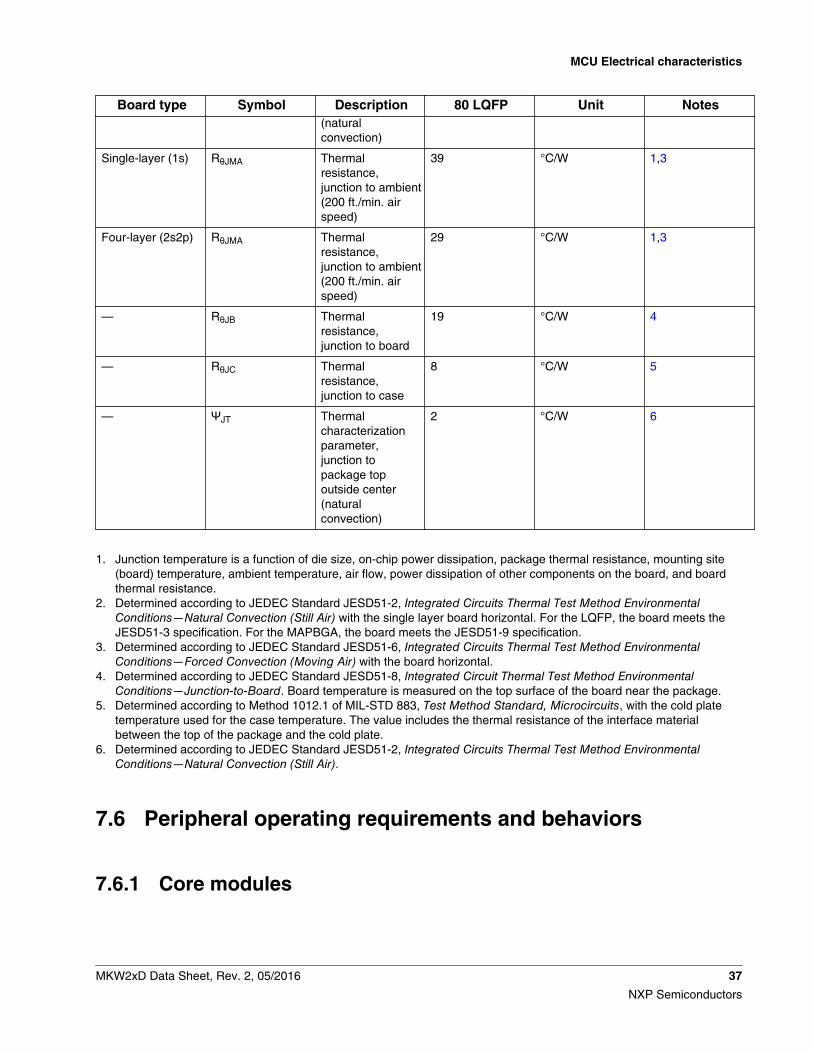
Board type Symbol Description 80 LQFP Unit Notes(naturalconvection)
Single-layer (1s) RθJMA Thermalresistance,junction to ambient(200 ft./min. airspeed)
39 °C/W 1,3
Four-layer (2s2p) RθJMA Thermalresistance,junction to ambient(200 ft./min. airspeed)
29 °C/W 1,3
— RθJB Thermalresistance,junction to board
19 °C/W 4
— RθJC Thermalresistance,junction to case
8 °C/W 5
— ΨJT Thermalcharacterizationparameter,junction topackage topoutside center(naturalconvection)
2 °C/W 6
1. Junction temperature is a function of die size, on-chip power dissipation, package thermal resistance, mounting site(board) temperature, ambient temperature, air flow, power dissipation of other components on the board, and boardthermal resistance.
2. Determined according to JEDEC Standard JESD51-2, Integrated Circuits Thermal Test Method EnvironmentalConditions—Natural Convection (Still Air) with the single layer board horizontal. For the LQFP, the board meets theJESD51-3 specification. For the MAPBGA, the board meets the JESD51-9 specification.
3. Determined according to JEDEC Standard JESD51-6, Integrated Circuits Thermal Test Method EnvironmentalConditions—Forced Convection (Moving Air) with the board horizontal.
4. Determined according to JEDEC Standard JESD51-8, Integrated Circuit Thermal Test Method EnvironmentalConditions—Junction-to-Board. Board temperature is measured on the top surface of the board near the package.
5. Determined according to Method 1012.1 of MIL-STD 883, Test Method Standard, Microcircuits, with the cold platetemperature used for the case temperature. The value includes the thermal resistance of the interface materialbetween the top of the package and the cold plate.
6. Determined according to JEDEC Standard JESD51-2, Integrated Circuits Thermal Test Method EnvironmentalConditions—Natural Convection (Still Air).
7.6 Peripheral operating requirements and behaviors
7.6.1 Core modules
MCU Electrical characteristics
MKW2xD Data Sheet, Rev. 2, 05/2016 37
NXP Semiconductors

7.6.1.1 JTAG electricalsTable 18. JTAG limited voltage range electricals
Symbol Description Min. Max. Unit
Operating voltage 2.7 3.6 V
J1 TCLK frequency of operation
• Boundary Scan
• JTAG and CJTAG
• Serial Wire Debug
0
0
0
10
25
50
MHz
J2 TCLK cycle period 1/J1 — ns
J3 TCLK clock pulse width
• Boundary Scan
• JTAG and CJTAG
• Serial Wire Debug
50
20
10
—
—
—
ns
ns
ns
J4 TCLK rise and fall times — 3 ns
J5 Boundary scan input data setup time to TCLK rise 20 — ns
J6 Boundary scan input data hold time after TCLK rise 0 — ns
J7 TCLK low to boundary scan output data valid — 25 ns
J8 TCLK low to boundary scan output high-Z — 25 ns
J9 TMS, TDI input data setup time to TCLK rise 8 — ns
J10 TMS, TDI input data hold time after TCLK rise 1 — ns
J11 TCLK low to TDO data valid — 17 ns
J12 TCLK low to TDO high-Z — 17 ns
J13 TRST assert time 100 — ns
J14 TRST setup time (negation) to TCLK high 8 — ns
Table 19. JTAG full voltage range electricals
Symbol Description Min. Max. Unit
Operating voltage 1.8 3.6 V
J1 TCLK frequency of operation
• Boundary Scan
• JTAG and CJTAG
• Serial Wire Debug
0
0
0
10
20
40
MHz
J2 TCLK cycle period 1/J1 — ns
J3 TCLK clock pulse width
• Boundary Scan
• JTAG and CJTAG
• Serial Wire Debug
50
25
12.5
—
—
—
ns
ns
ns
Table continues on the next page...
MCU Electrical characteristics
38 MKW2xD Data Sheet, Rev. 2, 05/2016
NXP Semiconductors

Table 19. JTAG full voltage range electricals (continued)
Symbol Description Min. Max. Unit
J4 TCLK rise and fall times — 3 ns
J5 Boundary scan input data setup time to TCLK rise 20 — ns
J6 Boundary scan input data hold time after TCLK rise 0 — ns
J7 TCLK low to boundary scan output data valid — 25 ns
J8 TCLK low to boundary scan output high-Z — 25 ns
J9 TMS, TDI input data setup time to TCLK rise 8 — ns
J10 TMS, TDI input data hold time after TCLK rise 1.4 — ns
J11 TCLK low to TDO data valid — 22.1 ns
J12 TCLK low to TDO high-Z — 22.1 ns
J13 TRST assert time 100 — ns
J14 TRST setup time (negation) to TCLK high 8 — ns
J2J3 J3
J4 J4
TCLK (input)
Figure 7. Test clock input timing
J7
J8
J7
J5 J6
Input data valid
Output data valid
Output data valid
TCLK
Data inputs
Data outputs
Data outputs
Data outputs
Figure 8. Boundary scan (JTAG) timing
MCU Electrical characteristics
MKW2xD Data Sheet, Rev. 2, 05/2016 39
NXP Semiconductors

J11
J12
J11
J9 J10
Input data valid
Output data valid
Output data valid
TCLK
TDI/TMS
TDO
TDO
TDO
Figure 9. Test Access Port timing
J14
J13
TCLK
TRST
Figure 10. TRST timing
7.6.2 System modules
There are no specifications necessary for the device's system modules.
7.6.3 Clock modules
MCU Electrical characteristics
40 MKW2xD Data Sheet, Rev. 2, 05/2016
NXP Semiconductors

7.6.3.1 MCG specificationsTable 20. MCG specifications
Symbol Description Min. Typ. Max. Unit Notes
fints_ft Internal reference frequency (slow clock) —factory trimmed at nominal VDD and 25 °C
— 32.768 — kHz
fints_t Internal reference frequency (slow clock) —user trimmed
31.25 — 39.0625 kHz
Δfdco_res_t Resolution of trimmed average DCO outputfrequency at fixed voltage and temperature —using SCTRIM and SCFTRIM
— ± 0.3 ± 0.6 %fdco 1
Δfdco_res_t Resolution of trimmed average DCO outputfrequency at fixed voltage and temperature —using SCTRIM only
— ± 0.2 ± 0.5 %fdco 1
Δfdco_t Total deviation of trimmed average DCO outputfrequency over voltage and temperature
— +0.5/-0.7 ± 2 %fdco 1, 2
Δfdco_t Total deviation of trimmed average DCO outputfrequency over fixed voltage and temperaturerange of 0–70°C
— ± 0.3 ±1 %fdco 1, 2
fintf_ft Internal reference frequency (fast clock) —factory trimmed at nominal VDD and 25°C
— 4 — MHz
fintf_t Internal reference frequency (fast clock) —user trimmed at nominal VDD and 25 °C
3 — 5 MHz
floc_low Loss of external clock minimum frequency —RANGE = 00
(3/5) xfints_t
— — kHz
floc_high Loss of external clock minimum frequency —RANGE = 01, 10, or 11
(16/5) xfints_t
— — kHz
FLL
ffll_ref FLL reference frequency range 31.25 — 39.0625 kHz
fdco DCO outputfrequency range
Low range (DRS=00)
640 × ffll_ref
20 20.97 25 MHz 3, 4
Mid range (DRS=01)
1280 × ffll_ref
40 41.94 50 MHz
Mid-high range (DRS=10)
1920 × ffll_ref
60 62.91 75 MHz
High range (DRS=11)
2560 × ffll_ref
80 83.89 100 MHz
fdco_t_DMX3
2
DCO outputfrequency
Low range (DRS=00)
732 × ffll_ref
— 23.99 — MHz 5,6
Mid range (DRS=01)
1464 × ffll_ref
— 47.97 — MHz
Mid-high range (DRS=10)
2197 × ffll_ref
— 71.99 — MHz
High range (DRS=11) — 95.98 — MHz
Table continues on the next page...
MCU Electrical characteristics
MKW2xD Data Sheet, Rev. 2, 05/2016 41
NXP Semiconductors

Table 20. MCG specifications (continued)
Symbol Description Min. Typ. Max. Unit Notes
2929 × ffll_ref
Jcyc_fll FLL period jitter
• fDCO = 48 MHz• fDCO = 98 MHz
—
—
180
150
—
—
ps
tfll_acquire FLL target frequency acquisition time — — 1 ms 7
PLL
fvco VCO operating frequency 48.0 — 100 MHz
Ipll PLL operating current• PLL @ 96 MHz (fosc_hi_1 = 8 MHz, fpll_ref
= 2 MHz, VDIV multiplier = 48)
— 1200 — µA8
Ipll PLL operating current• PLL @ 48 MHz (fosc_hi_1 = 8 MHz, fpll_ref
= 2 MHz, VDIV multiplier = 24)
— 700 — µA8
fpll_ref PLL reference frequency range 2.0 — 4.0 MHz
Jcyc_pll PLL period jitter (RMS)
• fvco = 48 MHz
• fvco = 100 MHz
—
—
120
75
—
—
ps
ps
9
Jacc_pll PLL accumulated jitter over 1µs (RMS)
• fvco = 48 MHz
• fvco = 100 MHz
—
—
1350
600
—
—
ps
ps
9
Dlock Lock entry frequency tolerance ± 1.49 — ± 2.98 %
Dunl Lock exit frequency tolerance ± 4.47 — ± 5.97 %
tpll_lock Lock detector detection time — — 150 × 10-6
+ 1075(1/fpll_ref)
s 10
1. This parameter is measured with the internal reference (slow clock) being used as a reference to the FLL (FEI clockmode).
2. 2 V <= VDD <= 3.6 V.3. These typical values listed are with the slow internal reference clock (FEI) using factory trim and DMX32=0.4. The resulting system clock frequencies should not exceed their maximum specified values. The DCO frequency
deviation (Δfdco_t) over voltage and temperature should be considered.5. These typical values listed are with the slow internal reference clock (FEI) using factory trim and DMX32=1.6. The resulting clock frequency must not exceed the maximum specified clock frequency of the device.7. This specification applies to any time the FLL reference source or reference divider is changed, trim value is changed,
DMX32 bit is changed, DRS bits are changed, or changing from FLL disabled (BLPE, BLPI) to FLL enabled (FEI, FEE,FBE, FBI). If a crystal/resonator is being used as the reference, this specification assumes it is already running.
8. Excludes any oscillator currents that are also consuming power while PLL is in operation.9. This specification was obtained using a Freescale developed PCB. PLL jitter is dependent on the noise characteristics of
each PCB and results will vary.10. This specification applies to any time the PLL VCO divider or reference divider is changed, or changing from PLL
disabled (BLPE, BLPI) to PLL enabled (PBE, PEE). If a crystal/resonator is being used as the reference, thisspecification assumes it is already running.
MCU Electrical characteristics
42 MKW2xD Data Sheet, Rev. 2, 05/2016
NXP Semiconductors

7.6.3.2 Oscillator electrical specifications
7.6.3.2.1 Oscillator DC electrical specificationsTable 21. Oscillator DC electrical specifications
Symbol Description Min. Typ. Max. Unit Notes
VDD Supply voltage 1.8 — 3.6 V
IDDOSC Supply current — low-power mode (HGO=0)
• 32 kHz
• 4 MHz
• 8 MHz (RANGE=01)
• 16 MHz
• 24 MHz
• 32 MHz
—
—
—
—
—
—
500
200
300
950
1.2
1.5
—
—
—
—
—
—
nA
μA
μA
μA
mA
mA
1
IDDOSC Supply current — high-gain mode (HGO=1)
• 32 kHz
• 4 MHz
• 8 MHz (RANGE=01)
• 16 MHz
• 24 MHz
• 32 MHz
—
—
—
—
—
—
5
500
600
2.5
3
4
—
—
—
—
—
—
μA
μA
μA
mA
mA
mA
1
Cx EXTAL load capacitance — — — 2, 3
Cy XTAL load capacitance — — — 2, 3
RF Feedback resistor — low-frequency, low-powermode (HGO=0)
— — — MΩ 2, 4
Feedback resistor — low-frequency, high-gainmode (HGO=1)
— 10 — MΩ
Feedback resistor — high-frequency, low-power mode (HGO=0)
— — — MΩ
Feedback resistor — high-frequency, high-gainmode (HGO=1)
— 1 — MΩ
RS Series resistor — low-frequency, low-powermode (HGO=0)
— — — kΩ
Series resistor — low-frequency, high-gainmode (HGO=1)
— 200 — kΩ
Series resistor — high-frequency, low-powermode (HGO=0)
— — — kΩ
Series resistor — high-frequency, high-gainmode (HGO=1)
—
0
—
kΩ
Table continues on the next page...
MCU Electrical characteristics
MKW2xD Data Sheet, Rev. 2, 05/2016 43
NXP Semiconductors

Table 21. Oscillator DC electrical specifications (continued)
Symbol Description Min. Typ. Max. Unit Notes
Vpp5 Peak-to-peak amplitude of oscillation (oscillator
mode) — low-frequency, low-power mode(HGO=0)
— 0.6 — V
Peak-to-peak amplitude of oscillation (oscillatormode) — low-frequency, high-gain mode(HGO=1)
— VDD — V
Peak-to-peak amplitude of oscillation (oscillatormode) — high-frequency, low-power mode(HGO=0)
— 0.6 — V
Peak-to-peak amplitude of oscillation (oscillatormode) — high-frequency, high-gain mode(HGO=1)
— VDD — V
1. VDD=3.3 V, Temperature =25 °C2. See crystal or resonator manufacturer's recommendation3. Cx and Cy can be provided by using either integrated capacitors or external components.4. When low-power mode is selected, RF is integrated and must not be attached externally.5. The EXTAL and XTAL pins should only be connected to required oscillator components and must not be connected to
any other device.
7.6.3.2.2 Oscillator frequency specificationsTable 22. Oscillator frequency specifications
Symbol Description Min. Typ. Max. Unit Notes
fosc_lo Oscillator crystal or resonator frequency — low-frequency mode (MCG_C2[RANGE]=00)
32 — 40 kHz
fosc_hi_1 Oscillator crystal or resonator frequency — high-frequency mode (low range)(MCG_C2[RANGE]=01)
3 — 8 MHz
fosc_hi_2 Oscillator crystal or resonator frequency — highfrequency mode (high range)(MCG_C2[RANGE]=1x)
8 — 32 MHz
fec_extal Input clock frequency (external clock mode) — — 50 MHz 1, 2
tdc_extal Input clock duty cycle (external clock mode) 40 50 60 %
tcst Crystal startup time — 32 kHz low-frequency,low-power mode (HGO=0)
— 750 — ms 3, 4
Crystal startup time — 32 kHz low-frequency,high-gain mode (HGO=1)
— 250 — ms
Crystal startup time — 8 MHz high-frequency(MCG_C2[RANGE]=01), low-power mode(HGO=0)
— 0.6 — ms
Crystal startup time — 8 MHz high-frequency(MCG_C2[RANGE]=01), high-gain mode(HGO=1)
— 1 — ms
1. Other frequency limits may apply when external clock is being used as a reference for the FLL or PLL.
MCU Electrical characteristics
44 MKW2xD Data Sheet, Rev. 2, 05/2016
NXP Semiconductors

2. When transitioning from FEI or FBI to FBE mode, restrict the frequency of the input clock so that, when it is divided byFRDIV, it remains within the limits of the DCO input clock frequency.
3. Proper PC board layout procedures must be followed to achieve specifications.4. Crystal startup time is defined as the time between the oscillator being enabled and the OSCINIT bit in the MCG_S
register being set.
NOTEThe 32 kHz oscillator works in low power mode by defaultand cannot be moved into high power/gain mode.
7.6.3.3 32 kHz oscillator electrical characteristics
7.6.3.3.1 32 kHz oscillator DC electrical specificationsTable 23. 32kHz oscillator DC electrical specifications
Symbol Description Min. Typ. Max. Unit
VBAT Supply voltage 1.8 — 3.6 V
RF Internal feedback resistor — 100 — MΩ
Cpara Parasitical capacitance of EXTAL32 andXTAL32
— 5 7 pF
Vpp1 Peak-to-peak amplitude of oscillation — 0.6 — V
1. When a crystal is being used with the 32 kHz oscillator, the EXTAL32 and XTAL32 pins should only be connected torequired oscillator components and must not be connected to any other devices.
7.6.3.3.2 32 kHz oscillator frequency specificationsTable 24. 32 kHz oscillator frequency specifications
Symbol Description Min. Typ. Max. Unit Notes
fosc_lo Oscillator crystal — 32.768 — kHz
tstart Crystal start-up time — 1000 — ms 1
vec_extal32 Externally provided input clock amplitude 700 — VBAT mV 2, 3
1. Proper PC board layout procedures must be followed to achieve specifications.2. This specification is for an externally supplied clock driven to EXTAL32 and does not apply to any other clock input.
The oscillator remains enabled and XTAL32 must be left unconnected.3. The parameter specified is a peak-to-peak value and VIH and VIL specifications do not apply. The voltage of the
applied clock must be within the range of VSS to VBAT.
7.6.4 Memories and memory interfaces
MCU Electrical characteristics
MKW2xD Data Sheet, Rev. 2, 05/2016 45
NXP Semiconductors

7.6.4.1 Flash electrical specifications
This section describes the electrical characteristics of the flash memory module.
7.6.4.1.1 Flash timing specifications — program and erase
The following specifications represent the amount of time the internal charge pumps areactive and do not include command overhead.
Table 25. NVM program/erase timing specifications
Symbol Description Min. Typ. Max. Unit Notes
thvpgm4 Longword Program high-voltage time — 7.5 18 μs —
thversscr Sector Erase high-voltage time — 13 113 ms 1
thversblk256k Erase Block high-voltage time for 256 KB — 104 904 ms 1
1. Maximum time based on expectations at cycling end-of-life.
7.6.4.1.2 Flash timing specifications — commandsTable 26. Flash command timing specifications
Symbol Description Min. Typ. Max. Unit Notes
trd1blk64k
trd1blk256k
Read 1s Block execution time
• 64 KB data flash
• 256 KB program flash
—
—
—
—
0.9
1.7
ms
ms
1
trd1sec2k Read 1s Section execution time (flash sector) — — 60 μs 1
tpgmchk Program Check execution time — — 45 μs 1
trdrsrc Read Resource execution time — — 30 μs 1
tpgm4 Program Longword execution time — 65 145 μs —
tersblk64k
tersblk256k
Erase Flash Block execution time
• 64 KB data flash
• 256 KB program flash
—
—
58
122
580
985
ms
ms
2
tersscr Erase Flash Sector execution time — 14 114 ms 2
tpgmsec512
tpgmsec1k
tpgmsec2k
Program Section execution time
• 512 bytes flash
• 1 KB flash
• 2 KB flash
—
—
—
2.4
4.7
9.3
—
—
—
ms
ms
ms
—
trd1all Read 1s All Blocks execution time — — 1.8 ms 1
trdonce Read Once execution time — — 25 μs 1
Table continues on the next page...
MCU Electrical characteristics
46 MKW2xD Data Sheet, Rev. 2, 05/2016
NXP Semiconductors
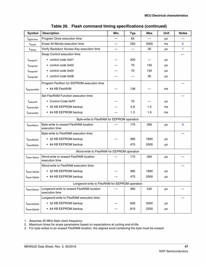
Table 26. Flash command timing specifications (continued)
Symbol Description Min. Typ. Max. Unit Notes
tpgmonce Program Once execution time — 65 — μs —
tersall Erase All Blocks execution time — 250 2000 ms 2
tvfykey Verify Backdoor Access Key execution time — — 30 μs 1
tswapx01
tswapx02
tswapx04
tswapx08
Swap Control execution time
• control code 0x01
• control code 0x02
• control code 0x04
• control code 0x08
—
—
—
—
200
70
70
—
—
150
150
30
μs
μs
μs
μs
—
tpgmpart64k
Program Partition for EEPROM execution time
• 64 KB FlexNVM
—
138
—
ms
—
tsetramff
tsetram32k
tsetram64k
Set FlexRAM Function execution time:
• Control Code 0xFF
• 32 KB EEPROM backup
• 64 KB EEPROM backup
—
—
—
70
0.8
1.3
—
1.2
1.9
μs
ms
ms
—
Byte-write to FlexRAM for EEPROM operation
teewr8bers Byte-write to erased FlexRAM locationexecution time
— 175 260 μs 3
teewr8b32k
teewr8b64k
Byte-write to FlexRAM execution time:
• 32 KB EEPROM backup
• 64 KB EEPROM backup
—
385
475
1800
2000
μs
μs
—
Word-write to FlexRAM for EEPROM operation
teewr16bers Word-write to erased FlexRAM locationexecution time
— 175 260 μs —
teewr16b32k
teewr16b64k
Word-write to FlexRAM execution time:
• 32 KB EEPROM backup
• 64 KB EEPROM backup
—
—
385
475
1800
2000
μs
μs
—
Longword-write to FlexRAM for EEPROM operation
teewr32bers Longword-write to erased FlexRAM locationexecution time
— 360 540 μs —
teewr32b32k
teewr32b64k
Longword-write to FlexRAM execution time:
• 32 KB EEPROM backup
• 64 KB EEPROM backup
—
—
630
810
2050
2250
μs
μs
—
1. Assumes 25 MHz flash clock frequency.2. Maximum times for erase parameters based on expectations at cycling end-of-life.3. For byte-writes to an erased FlexRAM location, the aligned word containing the byte must be erased.
MCU Electrical characteristics
MKW2xD Data Sheet, Rev. 2, 05/2016 47
NXP Semiconductors

7.6.4.1.3 Flash high voltage current behaviorsTable 27. Flash high voltage current behaviors
Symbol Description Min. Typ. Max. Unit
IDD_PGM Average current adder during high voltageflash programming operation
— 2.5 6.0 mA
IDD_ERS Average current adder during high voltageflash erase operation
— 1.5 4.0 mA
7.6.4.1.4 Reliability specificationsTable 28. NVM reliability specifications
Symbol Description Min. Typ.1 Max. Unit Notes
Program Flash
tnvmretp10k Data retention after up to 10 K cycles 5 50 — years —
tnvmretp1k Data retention after up to 1 K cycles 20 100 — years —
nnvmcycp Cycling endurance 10 K 50 K — cycles 2
Data Flash
tnvmretd10k Data retention after up to 10 K cycles 5 50 — years —
tnvmretd1k Data retention after up to 1 K cycles 20 100 — years —
nnvmcycd Cycling endurance 10 K 50 K — cycles 2
FlexRAM as EEPROM
tnvmretee100 Data retention up to 100% of write endurance 5 50 — years —
tnvmretee10 Data retention up to 10% of write endurance 20 100 — years —
nnvmwree16
nnvmwree128
nnvmwree512
nnvmwree4k
Write endurance
• EEPROM backup to FlexRAM ratio = 16
• EEPROM backup to FlexRAM ratio = 128
• EEPROM backup to FlexRAM ratio = 512
• EEPROM backup to FlexRAM ratio =4096
35 K
315 K
1.27 M
10 M
175 K
1.6 M
6.4 M
50 M
—
—
—
—
writes
writes
writes
writes
3
1. Typical data retention values are based on measured response accelerated at high temperature and derated to aconstant 25 °C use profile. Engineering Bulletin EB618 does not apply to this technology. Typical endurance defined inEngineering Bulletin EB619.
2. Cycling endurance represents number of program/erase cycles at –40 °C ≤ Tj ≤ °C.3. Write endurance represents the number of writes to each FlexRAM location at –40 °C ≤Tj ≤ °C influenced by the cycling
endurance of the FlexNVM (same value as data flash) and the allocated EEPROM backup per subsystem. Minimum andtypical values assume all byte-writes to FlexRAM.
MCU Electrical characteristics
48 MKW2xD Data Sheet, Rev. 2, 05/2016
NXP Semiconductors

7.6.4.2 EzPort switching specificationsTable 29. EzPort switching specifications
Num Description Min. Max. Unit
Operating voltage 1.8 3.6 V
EP1 EZP_CK frequency of operation (all commands exceptREAD)
— fSYS/2 MHz
EP1a EZP_CK frequency of operation (READ command) — fSYS/8 MHz
EP2 EZP_CS negation to next EZP_CS assertion 2 x tEZP_CK — ns
EP3 EZP_CS input valid to EZP_CK high (setup) 5 — ns
EP4 EZP_CK high to EZP_CS input invalid (hold) 5 — ns
EP5 EZP_D input valid to EZP_CK high (setup) 2 — ns
EP6 EZP_CK high to EZP_D input invalid (hold) 5 — ns
EP7 EZP_CK low to EZP_Q output valid — ns
EP8 EZP_CK low to EZP_Q output invalid (hold) 0 — ns
EP9 EZP_CS negation to EZP_Q tri-state — 12 ns
EP2EP3 EP4
EP5 EP6
EP7 EP8
EP9
EZP_CK
EZP_CS
EZP_Q (output)
EZP_D (input)
Figure 11. EzPort Timing Diagram
7.6.5 Security and integrity modules
MCU Electrical characteristics
MKW2xD Data Sheet, Rev. 2, 05/2016 49
NXP Semiconductors

7.6.5.1 DryIce Tamper Electrical Specifications
Information about security-related modules is not included in this document and isavailable only after a nondisclosure agreement (NDA) has been signed. To request anNDA, contact your local NXP sales representative.
7.6.6 Analog
7.6.6.1 ADC electrical specifications
The 16-bit accuracy specifications listed in Table 1 and Table 31 are achievable on thedifferential pins ADCx_DP0, ADCx_DM0.
All other ADC channels meet the 13-bit differential/12-bit single-ended accuracyspecifications.
7.6.6.1.1 16-bit ADC operating conditionsTable 30. 16-bit ADC operating conditions
Symbol Description Conditions Min. Typ.1 Max. Unit Notes
VDDA Supply voltage Absolute 1.8 — 3.6 V
ΔVDDA Supply voltage Delta to VDD (VDD – VDDA) -100 0 +100 mV 2
ΔVSSA Ground voltage Delta to VSS (VSS – VSSA) -100 0 +100 mV 2
VREFH ADC referencevoltage high
Absolute VDDA VDDA VDDA V 3
VREFL ADC referencevoltage low
Absolute VSSA VSSA VSSA V 4
VADIN Input voltage • 16-bit differential mode
• All other modes
VREFL
VREFL
—
—
31/32 *VREFH
VREFH
V
CADIN Inputcapacitance
• 16-bit mode
• 8-bit / 10-bit / 12-bitmodes
—
—
8
4
10
5
pF
RADIN Input seriesresistance
— 2 5 kΩ
RAS Analog sourceresistance(external)
13-bit / 12-bit modes
fADCK < 4 MHz
—
—
5
kΩ
5
fADCK ADC conversionclock frequency
≤ 13-bit mode 1.0 — 18.0 MHz 6
Table continues on the next page...
MCU Electrical characteristics
50 MKW2xD Data Sheet, Rev. 2, 05/2016
NXP Semiconductors

Table 30. 16-bit ADC operating conditions (continued)
Symbol Description Conditions Min. Typ.1 Max. Unit Notes
fADCK ADC conversionclock frequency
16-bit mode 2.0 — 12.0 MHz 6
Crate ADC conversionrate
≤ 13-bit modes
No ADC hardware averaging
Continuous conversionsenabled, subsequentconversion time
20.000
—
818.330
Ksps
7
Crate ADC conversionrate
16-bit mode
No ADC hardware averaging
Continuous conversionsenabled, subsequentconversion time
37.037
—
461.467
Ksps
7
1. Typical values assume VDDA = 3.0 V, Temp = 25 °C, fADCK = 1.0 MHz, unless otherwise stated. Typical values are forreference only, and are not tested in production.
2. DC potential difference.3. VREFH is internally tied to VDDA.4. VREFL is internally tied to VSSA.5. This resistance is external to MCU. To achieve the best results, the analog source resistance must be kept as low as
possible. The results in this data sheet were derived from a system that had < 8 Ω analog source resistance. TheRAS/CAS time constant should be kept to < 1 ns.
6. To use the maximum ADC conversion clock frequency, CFG2[ADHSC] must be set and CFG1[ADLPC] must be clear.7. For guidelines and examples of conversion rate calculation, download the ADC calculator tool.
RAS
VAS CAS
ZAS
VADIN
ZADIN
RADIN
RADIN
RADIN
RADIN
CADIN
Pad leakagedue toinput protection
INPUT PIN
INPUT PIN
INPUT PIN
SIMPLIFIEDINPUT PIN EQUIVALENT
CIRCUITSIMPLIFIED
CHANNEL SELECTCIRCUIT ADC SAR
ENGINE
Figure 12. ADC input impedance equivalency diagram
MCU Electrical characteristics
MKW2xD Data Sheet, Rev. 2, 05/2016 51
NXP Semiconductors

7.6.6.1.2 16-bit ADC electrical characteristics
Table 31. 16-bit ADC characteristics (VREFH = VDDA, VREFL = VSSA)
Symbol Description Conditions1 Min. Typ.2 Max. Unit Notes
IDDA_ADC Supply current 0.215 — 1.7 mA 3
fADACK
ADC asynchronousclock source
• ADLPC = 1, ADHSC = 0
• ADLPC = 1, ADHSC = 1
• ADLPC = 0, ADHSC = 0
• ADLPC = 0, ADHSC = 1
1.2
2.4
3.0
4.4
2.4
4.0
5.2
6.2
3.9
6.1
7.3
9.5
MHz
MHz
MHz
MHz
tADACK = 1/fADACK
Sample Time See Reference Manual chapter for sample times
TUE Total unadjustederror
• 12-bit modes
• <12-bit modes
—
—
±4
±1.4
±6.8
±2.1
LSB4 5
DNL Differential non-linearity
• 12-bit modes
• <12-bit modes
—
—
±0.7
±0.2
–1.1 to+1.9
–0.3 to0.5
LSB4 5
INL Integral non-linearity • 12-bit modes
• <12-bit modes
—
—
±1.0
±0.5
–2.7 to+1.9
–0.7 to+0.5
LSB4 5
EFS Full-scale error • 12-bit modes
• <12-bit modes
—
—
–4
–1.4
–5.4
–1.8
LSB4 VADIN = VDDA5
EQ Quantization error • 16-bit modes
• ≤13-bit modes
—
—
–1 to 0
—
—
±0.5
LSB4
ENOB Effective number ofbits
16-bit differential mode
• Avg = 32
• Avg = 4
16-bit single-ended mode
• Avg = 32
• Avg = 4
12.8
11.9
12.2
11.4
14.5
13.8
13.9
13.1
—
—
—
—
bits
bits
bits
bits
6
SINADSignal-to-noise plusdistortion
See ENOB6.02 × ENOB + 1.76 dB
THD Total harmonicdistortion
16-bit differential mode
• Avg = 32
16-bit single-ended mode
—
—
-94
-85
—
—
dB
dB
7
Table continues on the next page...
MCU Electrical characteristics
52 MKW2xD Data Sheet, Rev. 2, 05/2016
NXP Semiconductors

Table 31. 16-bit ADC characteristics (VREFH = VDDA, VREFL = VSSA) (continued)
Symbol Description Conditions1 Min. Typ.2 Max. Unit Notes
• Avg = 32
SFDR Spurious freedynamic range
16-bit differential mode
• Avg = 32
16-bit single-ended mode
• Avg = 32
82
78
95
90
—
—
dB
dB
7
EIL Input leakage error IIn × RAS mV IIn = leakagecurrent
(refer to theMCU's voltage
and currentoperatingratings)
Temp sensor slope Across the full temperaturerange of the device
1.55 1.62 1.69 mV/°C 8
VTEMP25 Temp sensor voltage 25 °C 706 716 726 mV 8
1. All accuracy numbers assume the ADC is calibrated with VREFH = VDDA2. Typical values assume VDDA = 3.0 V, Temp = 25 °C, fADCK = 2.0 MHz unless otherwise stated. Typical values are for
reference only and are not tested in production.3. The ADC supply current depends on the ADC conversion clock speed, conversion rate and ADC_CFG1[ADLPC] (low
power). For lowest power operation, ADC_CFG1[ADLPC] must be set, the ADC_CFG2[ADHSC] bit must be clear with1 MHz ADC conversion clock speed.
4. 1 LSB = (VREFH - VREFL)/2N
5. ADC conversion clock < 16 MHz, Max hardware averaging (AVGE = %1, AVGS = %11)6. Input data is 100 Hz sine wave. ADC conversion clock < 12 MHz.7. Input data is 1 kHz sine wave. ADC conversion clock < 12 MHz.8. ADC conversion clock < 3 MHz
MCU Electrical characteristics
MKW2xD Data Sheet, Rev. 2, 05/2016 53
NXP Semiconductors

Typical ADC 16-bit Differential ENOB vs ADC Clock100Hz, 90% FS Sine Input
ENO
B
ADC Clock Frequency (MHz)
15.00
14.70
14.40
14.10
13.80
13.50
13.20
12.90
12.60
12.30
12.001 2 3 4 5 6 7 8 9 10 1211
Hardware Averaging DisabledAveraging of 4 samplesAveraging of 8 samplesAveraging of 32 samples
Figure 13. Typical ENOB vs. ADC_CLK for 16-bit differential mode
Typical ADC 16-bit Single-Ended ENOB vs ADC Clock100Hz, 90% FS Sine Input
ENO
B
ADC Clock Frequency (MHz)
14.00
13.75
13.25
13.00
12.75
12.50
12.00
11.75
11.50
11.25
11.001 2 3 4 5 6 7 8 9 10 1211
Averaging of 4 samplesAveraging of 32 samples
13.50
12.25
Figure 14. Typical ENOB vs. ADC_CLK for 16-bit single-ended mode
7.6.6.2 CMP and 6-bit DAC electrical specificationsTable 32. Comparator and 6-bit DAC electrical specifications
Symbol Description Min. Typ. Max. Unit
VDD Supply voltage 1.8 — 3.6 V
IDDHS Supply current, High-speed mode (EN=1, PMODE=1) — — 200 μA
Table continues on the next page...
MCU Electrical characteristics
54 MKW2xD Data Sheet, Rev. 2, 05/2016
NXP Semiconductors

Table 32. Comparator and 6-bit DAC electrical specifications (continued)
Symbol Description Min. Typ. Max. Unit
IDDLS Supply current, low-speed mode (EN=1, PMODE=0) — — 20 μA
VAIN Analog input voltage VSS – 0.3 — VDD V
VAIO Analog input offset voltage — — 20 mV
VH Analog comparator hysteresis1
• CR0[HYSTCTR] = 00
• CR0[HYSTCTR] = 01
• CR0[HYSTCTR] = 10
• CR0[HYSTCTR] = 11
—
—
—
—
5
10
20
30
—
—
—
—
mV
mV
mV
mV
VCMPOh Output high VDD – 0.5 — — V
VCMPOl Output low — — 0.5 V
tDHS Propagation delay, high-speed mode (EN=1,PMODE=1)
20 50 200 ns
tDLS Propagation delay, low-speed mode (EN=1,PMODE=0)
80 250 600 ns
Analog comparator initialization delay2 — — 40 μs
IDAC6b 6-bit DAC current adder (enabled) — 7 — μA
INL 6-bit DAC integral non-linearity –0.5 — 0.5 LSB3
DNL 6-bit DAC differential non-linearity –0.3 — 0.3 LSB
1. Typical hysteresis is measured with input voltage range limited to 0.6 to VDD–0.6 V.2. Comparator initialization delay is defined as the time between software writes to change control inputs (Writes to
CMP_DACCR[DACEN], CMP_DACCR[VRSEL], CMP_DACCR[VOSEL], CMP_MUXCR[PSEL], andCMP_MUXCR[MSEL]) and the comparator output settling to a stable level.
3. 1 LSB = Vreference/64
MCU Electrical characteristics
MKW2xD Data Sheet, Rev. 2, 05/2016 55
NXP Semiconductors

00
01
10
HYSTCTR Setting
0.1
10
11
Vin level (V)
CM
P H
yste
reris
(V)
3.12.82.52.21.91.61.310.70.4
0.05
0
0.01
0.02
0.03
0.08
0.07
0.06
0.04
Figure 15. Typical hysteresis vs. Vin level (VDD = 3.3 V, PMODE = 0)
MCU Electrical characteristics
56 MKW2xD Data Sheet, Rev. 2, 05/2016
NXP Semiconductors

000110
HYSTCTR Setting
1011
0.1 3.12.82.52.21.91.61.310.70.4
0.1
0
0.02
0.04
0.06
0.18
0.14
0.12
0.08
0.16
Vin level (V)
CM
P H
yste
resi
s (V
)
Figure 16. Typical hysteresis vs. Vin level (VDD = 3.3 V, PMODE = 1)
7.6.7 Timers
See General switching specifications.
7.6.8 Communication interfaces
7.6.8.1 USB electrical specificationsThe USB electricals for the USB On-the-Go module conform to the standardsdocumented by the Universal Serial Bus Implementers Forum. For the most up-to-date standards, visit usb.org.
NOTE
MCU Electrical characteristics
MKW2xD Data Sheet, Rev. 2, 05/2016 57
NXP Semiconductors

7.6.8.2 USB DCD electrical specificationsTable 33. USB0 DCD electrical specifications
Symbol Description Min. Typ. Max. Unit
VDP_SRC USB_DP source voltage (up to 250 μA) 0.5 — 0.7 V
VLGC Threshold voltage for logic high 0.8 — 2.0 V
IDP_SRC USB_DP source current 7 10 13 μA
IDM_SINK USB_DM sink current 50 100 150 μA
RDM_DWN D- pulldown resistance for data pin contact detect 14.25 — 24.8 kΩ
VDAT_REF Data detect voltage 0.25 0.33 0.4 V
7.6.8.3 VREG electrical specificationsTable 34. VREG electrical specifications
Symbol Description Min. Typ.1 Max. Unit Notes
VREGIN Input supply voltage 2.7 — 5.5 V
IDDon Quiescent current — Run mode, load currentequal zero, input supply (VREGIN) > 3.6 V
— 125 186 μA
IDDstby Quiescent current — Standby mode, loadcurrent equal zero
— 1.27 30 μA
IDDoff Quiescent current — Shutdown mode
• VREGIN = 5.0 V and temperature=25 °C
• Across operating voltage and temperature
—
—
650
—
—
4
nA
μA
ILOADrun Maximum load current — Run mode — — 120 mA
ILOADstby Maximum load current — Standby mode — — 1 mA
VReg33out Regulator output voltage — Input supply(VREGIN) > 3.6 V
• Run mode
• Standby mode
3
2.1
3.3
2.8
3.6
3.6
V
V
VReg33out Regulator output voltage — Input supply(VREGIN) < 3.6 V, pass-through mode
2.1 — 3.6 V 2
COUT External output capacitor 1.76 2.2 8.16 μF
ESR External output capacitor equivalent seriesresistance
1 — 100 mΩ
ILIM Short circuit current — 290 — mA
1. Typical values assume VREGIN = 5.0 V, Temp = 25 °C unless otherwise stated.2. Operating in pass-through mode: regulator output voltage equal to the input voltage minus a drop proportional to ILoad.
MCU Electrical characteristics
58 MKW2xD Data Sheet, Rev. 2, 05/2016
NXP Semiconductors

7.6.8.4 DSPI switching specifications (limited voltage range)
The DMA Serial Peripheral Interface (DSPI) provides a synchronous serial bus withmaster and slave operations. Many of the transfer attributes are programmable. Thetables below provide DSPI timing characteristics for classic SPI timing modes. Referto the DSPI chapter of the Reference Manual for information on the modified transferformats used for communicating with slower peripheral devices.
Table 35. Master mode DSPI timing (limited voltage range)
Num Description Min. Max. Unit Notes
Operating voltage 2.7 3.6 V
Frequency of operation — 25 MHz
DS1 DSPI_SCK output cycle time 2 x tBUS — ns
DS2 DSPI_SCK output high/low time (tSCK/2) − 2 (tSCK/2) + 2 ns
DS3 DSPI_PCSn valid to DSPI_SCK delay (tBUS x 2) −2
— ns 1
DS4 DSPI_SCK to DSPI_PCSn invalid delay (tBUS x 2) −2
— ns 2
DS5 DSPI_SCK to DSPI_SOUT valid — 8.5 ns
DS6 DSPI_SCK to DSPI_SOUT invalid −2 — ns
DS7 DSPI_SIN to DSPI_SCK input setup 15 — ns
DS8 DSPI_SCK to DSPI_SIN input hold 0 — ns
1. The delay is programmable in SPIx_CTARn[PSSCK] and SPIx_CTARn[CSSCK].2. The delay is programmable in SPIx_CTARn[PASC] and SPIx_CTARn[ASC].
DS3 DS4DS1DS2
DS7DS8
First data Last dataDS5
First data Data Last data
DS6
Data
DSPI_PCSn
DSPI_SCK
(CPOL=0)
DSPI_SIN
DSPI_SOUT
Figure 17. DSPI classic SPI timing — master mode
Table 36. Slave mode DSPI timing (limited voltage range)
Num Description Min. Max. Unit
Operating voltage 2.7 3.6 V
Frequency of operation 12.5 MHz
Table continues on the next page...
MCU Electrical characteristics
MKW2xD Data Sheet, Rev. 2, 05/2016 59
NXP Semiconductors

Table 36. Slave mode DSPI timing (limited voltage range) (continued)
Num Description Min. Max. Unit
DS9 DSPI_SCK input cycle time 4 x tBUS — ns
DS10 DSPI_SCK input high/low time (tSCK/2) − 2 (tSCK/2) + 2 ns
DS11 DSPI_SCK to DSPI_SOUT valid — 10 ns
DS12 DSPI_SCK to DSPI_SOUT invalid 0 — ns
DS13 DSPI_SIN to DSPI_SCK input setup 2 — ns
DS14 DSPI_SCK to DSPI_SIN input hold 7 — ns
DS15 DSPI_SS active to DSPI_SOUT driven — 14 ns
DS16 DSPI_SS inactive to DSPI_SOUT not driven — 14 ns
First data Last data
First data Data Last data
Data
DS15
DS10 DS9
DS16DS11DS12
DS14DS13
DSPI_SS
DSPI_SCK
(CPOL=0)
DSPI_SOUT
DSPI_SIN
Figure 18. DSPI classic SPI timing — slave mode
7.6.8.5 DSPI switching specifications (full voltage range)
The DMA Serial Peripheral Interface (DSPI) provides a synchronous serial bus withmaster and slave operations. Many of the transfer attributes are programmable. Thetables below provides DSPI timing characteristics for classic SPI timing modes. Referto the DSPI chapter of the Reference Manual for information on the modified transferformats used for communicating with slower peripheral devices.
Table 37. Master mode DSPI timing (full voltage range)
Num Description Min. Max. Unit Notes
Operating voltage 1.8 3.6 V 1
Frequency of operation — 12.5 MHz
DS1 DSPI_SCK output cycle time 4 x tBUS — ns
DS2 DSPI_SCK output high/low time (tSCK/2) - 4 (tSCK/2) + 4 ns
Table continues on the next page...
MCU Electrical characteristics
60 MKW2xD Data Sheet, Rev. 2, 05/2016
NXP Semiconductors

Table 37. Master mode DSPI timing (full voltage range) (continued)
Num Description Min. Max. Unit Notes
DS3 DSPI_PCSn valid to DSPI_SCK delay (tBUS x 2) −4
— ns 2
DS4 DSPI_SCK to DSPI_PCSn invalid delay (tBUS x 2) −4
— ns 3
DS5 DSPI_SCK to DSPI_SOUT valid — 10 ns
DS6 DSPI_SCK to DSPI_SOUT invalid -4.5 — ns
DS7 DSPI_SIN to DSPI_SCK input setup 20.5 — ns
DS8 DSPI_SCK to DSPI_SIN input hold 0 — ns
1. The DSPI module can operate across the entire operating voltage for the processor, but to run across the full voltagerange the maximum frequency of operation is reduced.
2. The delay is programmable in SPIx_CTARn[PSSCK] and SPIx_CTARn[CSSCK].3. The delay is programmable in SPIx_CTARn[PASC] and SPIx_CTARn[ASC].
DS3 DS4DS1DS2
DS7DS8
First data Last dataDS5
First data Data Last data
DS6
Data
DSPI_PCSn
DSPI_SCK
(CPOL=0)
DSPI_SIN
DSPI_SOUT
Figure 19. DSPI classic SPI timing — master mode
Table 38. Slave mode DSPI timing (full voltage range)
Num Description Min. Max. Unit
Operating voltage 1.8 3.6 V
Frequency of operation — 6.25 MHz
DS9 DSPI_SCK input cycle time 8 x tBUS — ns
DS10 DSPI_SCK input high/low time (tSCK/2) - 4 (tSCK/2) + 4 ns
DS11 DSPI_SCK to DSPI_SOUT valid — 20 ns
DS12 DSPI_SCK to DSPI_SOUT invalid 0 — ns
DS13 DSPI_SIN to DSPI_SCK input setup 2 — ns
DS14 DSPI_SCK to DSPI_SIN input hold 7 — ns
DS15 DSPI_SS active to DSPI_SOUT driven — 19 ns
DS16 DSPI_SS inactive to DSPI_SOUT not driven — 19 ns
MCU Electrical characteristics
MKW2xD Data Sheet, Rev. 2, 05/2016 61
NXP Semiconductors

First data Last data
First data Data Last data
Data
DS15
DS10 DS9
DS16DS11DS12
DS14DS13
DSPI_SS
DSPI_SCK
(CPOL=0)
DSPI_SOUT
DSPI_SIN
Figure 20. DSPI classic SPI timing — slave mode
7.6.8.6 I2C
See General switching specifications.
7.6.8.7 UART
See General switching specifications.
7.6.8.8 Normal Run, Wait and Stop mode performance over the fulloperating voltage range
This section provides the operating performance over the full operating voltage for thedevice in Normal Run, Wait and Stop modes.
Due to a limited set of pin availability in the SiP, the I2S/SAI block is usable only forreceive mode and must be configured as a slave.
Table 39. I2S/SAI master mode timing
Num. Characteristic Min. Max. Unit
Operating voltage 1.8 3.6 V
S1 I2S_MCLK cycle time 40 — ns
S2 I2S_MCLK (as an input) pulse width high/low 45% 55% MCLK period
S3 I2S_TX_BCLK/I2S_RX_BCLK cycle time (output) 80 — ns
S4 I2S_TX_BCLK/I2S_RX_BCLK pulse width high/low 45% 55% BCLK period
S5 I2S_TX_BCLK/I2S_RX_BCLK to I2S_TX_FS/I2S_RX_FS output valid
— 15 ns
S6 I2S_TX_BCLK/I2S_RX_BCLK to I2S_TX_FS/I2S_RX_FS output invalid
0 — ns
Table continues on the next page...
MCU Electrical characteristics
62 MKW2xD Data Sheet, Rev. 2, 05/2016
NXP Semiconductors

Table 39. I2S/SAI master mode timing (continued)
Num. Characteristic Min. Max. Unit
S7 I2S_TX_BCLK to I2S_TXD valid — 15 ns
S8 I2S_TX_BCLK to I2S_TXD invalid 0 — ns
S9 I2S_RXD/I2S_RX_FS input setup beforeI2S_RX_BCLK
25 — ns
S10 I2S_RXD/I2S_RX_FS input hold after I2S_RX_BCLK 0 — ns
S1 S2 S2
S3
S4S4
S5
S9
S7
S9 S10
S7
S8
S6
S10
S8
I2S_MCLK (output)
I2S_TX_BCLK/ I2S_RX_BCLK (output)
I2S_TX_FS/ I2S_RX_FS (output)
I2S_TX_FS/ I2S_RX_FS (input)
I2S_TXD
I2S_RXD
Figure 21. I2S/SAI timing — master modes
Table 40. I2S/SAI slave mode timing
Num. Characteristic Min. Max. Unit
Operating voltage 1.8 3.6 V
S11 I2S_TX_BCLK/I2S_RX_BCLK cycle time (input) 80 — ns
S12 I2S_TX_BCLK/I2S_RX_BCLK pulse width high/low(input)
45% 55% MCLK period
S13 I2S_TX_FS/I2S_RX_FS input setup beforeI2S_TX_BCLK/I2S_RX_BCLK
10 — ns
S14 I2S_TX_FS/I2S_RX_FS input hold afterI2S_TX_BCLK/I2S_RX_BCLK
2 — ns
S15 I2S_TX_BCLK to I2S_TXD/I2S_TX_FS output valid — 29 ns
S16 I2S_TX_BCLK to I2S_TXD/I2S_TX_FS outputinvalid
0 — ns
S17 I2S_RXD setup before I2S_RX_BCLK 10 — ns
S18 I2S_RXD hold after I2S_RX_BCLK 2 — ns
S19 I2S_TX_FS input assertion to I2S_TXD output valid1 — 21 ns
MCU Electrical characteristics
MKW2xD Data Sheet, Rev. 2, 05/2016 63
NXP Semiconductors

1. Applies to first bit in each frame and only if the TCR4[FSE] bit is clear
S15
S13
S15
S17 S18
S15
S16
S16
S14
S16
S11
S12S12
I2S_TX_BCLK/ I2S_RX_BCLK (input)
I2S_TX_FS/ I2S_RX_FS (output)
I2S_TXD
I2S_RXD
I2S_TX_FS/ I2S_RX_FS (input) S19
Figure 22. I2S/SAI timing — slave modes
7.6.8.9 VLPR, VLPW, and VLPS mode performance over the fulloperating voltage range
This section provides the operating performance over the full operating voltage for thedevice in VLPR, VLPW, and VLPS modes.
Due to a limited set of pin availability in the SiP, the I2S/SAI block is usable only forreceive mode and must be configured as a slave.
Table 41. I2S/SAI master mode timing in VLPR, VLPW, and VLPS modes (full voltage range)
Num. Characteristic Min. Max. Unit
Operating voltage 1.8 3.6 V
S1 I2S_MCLK cycle time 62.5 — ns
S2 I2S_MCLK pulse width high/low 45% 55% MCLK period
S3 I2S_TX_BCLK/I2S_RX_BCLK cycle time (output) 250 — ns
S4 I2S_TX_BCLK/I2S_RX_BCLK pulse width high/low 45% 55% BCLK period
S5 I2S_TX_BCLK/I2S_RX_BCLK to I2S_TX_FS/I2S_RX_FS output valid
— 45 ns
S6 I2S_TX_BCLK/I2S_RX_BCLK to I2S_TX_FS/I2S_RX_FS output invalid
0 — ns
S7 I2S_TX_BCLK to I2S_TXD valid — 45 ns
S8 I2S_TX_BCLK to I2S_TXD invalid 0 — ns
S9 I2S_RXD/I2S_RX_FS input setup beforeI2S_RX_BCLK
75 — ns
S10 I2S_RXD/I2S_RX_FS input hold after I2S_RX_BCLK 0 — ns
MCU Electrical characteristics
64 MKW2xD Data Sheet, Rev. 2, 05/2016
NXP Semiconductors

S1 S2 S2
S3
S4S4
S5
S9
S7
S9 S10
S7
S8
S6
S10
S8
I2S_MCLK (output)
I2S_TX_BCLK/ I2S_RX_BCLK (output)
I2S_TX_FS/ I2S_RX_FS (output)
I2S_TX_FS/ I2S_RX_FS (input)
I2S_TXD
I2S_RXD
Figure 23. I2S/SAI timing — master modes
Table 42. I2S/SAI slave mode timing in VLPR, VLPW, and VLPS modes (full voltage range)
Num. Characteristic Min. Max. Unit
Operating voltage 1.8 3.6 V
S11 I2S_TX_BCLK/I2S_RX_BCLK cycle time (input) 250 — ns
S12 I2S_TX_BCLK/I2S_RX_BCLK pulse width high/low(input)
45% 55% MCLK period
S13 I2S_TX_FS/I2S_RX_FS input setup beforeI2S_TX_BCLK/I2S_RX_BCLK
30 — ns
S14 I2S_TX_FS/I2S_RX_FS input hold afterI2S_TX_BCLK/I2S_RX_BCLK
2 — ns
S15 I2S_TX_BCLK to I2S_TXD/I2S_TX_FS output valid — 87 ns
S16 I2S_TX_BCLK to I2S_TXD/I2S_TX_FS outputinvalid
0 — ns
S17 I2S_RXD setup before I2S_RX_BCLK 30 — ns
S18 I2S_RXD hold after I2S_RX_BCLK 2 — ns
S19 I2S_TX_FS input assertion to I2S_TXD output valid1 — 72 ns
1. Applies to first bit in each frame and only if the TCR4[FSE] bit is clear
MCU Electrical characteristics
MKW2xD Data Sheet, Rev. 2, 05/2016 65
NXP Semiconductors

S15
S13
S15
S17 S18
S15
S16
S16
S14
S16
S11
S12S12
I2S_TX_BCLK/ I2S_RX_BCLK (input)
I2S_TX_FS/ I2S_RX_FS (output)
I2S_TXD
I2S_RXD
I2S_TX_FS/ I2S_RX_FS (input) S19
Figure 24. I2S/SAI timing — slave modes
Transceiver Electrical Characteristics
8.1 DC electrical characteristicsTable 43. DC electrical characteristics (VBAT, VBAT2 = 2.7 V, TA=25 °C, unless otherwise
noted)
Characteristic Symbol Min Typ Max Unit
Power Supply Current (VBAT + VBAT2)
Reset / power down1 Ileakage — <60 <100 nA
Hibernate1 ICCH — <1 — μA
Doze (No CLK_OUT) ICCD — 500 — μA
Idle (No CLK_OUT) ICCI — 700 — μA
Transmit mode (0 dBm nominal output power) ICCT — 17 18 mA
Receive mode (normal)
Receive mode (power preamble search)
ICCR — 19
15 (LPPS)
19.5 mA
Input current (VIN = 0 V or VDDINT) (All digital inputs) IIN — — ±1 μA
Input low voltage (all digital inputs) VIL 0 — 30%VDDINT
V
Input high voltage (all digital inputs) VIH 70%VDDINT
— VDDINT V
Output high voltage (IOH = -1 mA) (all digital outputs) VOH 80%VDDINT
— VDDINT V
Output low voltage (IOL = 1 mA) (all digital outputs) VOL 0 — 20%VDDINT
V
1. To attain specified low power current, all GPIO and other digital IO must be handled properly.
8
Transceiver Electrical Characteristics
66 MKW2xD Data Sheet, Rev. 2, 05/2016
NXP Semiconductors

8.2 AC electrical characteristicsTable 44. Receiver AC electrical characteristics (VBAT, VDDINT = 2.7 V, TA=25 °C, fref = 32 MHz
unless otherwise noted)
Characteristic Symbol Min Typ Max Unit
Sensitivity for 1% packet error rate (PER) (–40 to +105 °C) SENSper — –99 –97 dBm
Sensitivity for 1% packet error rate (PER) (+25 °C) SENSper — –102 dBm
Saturation (maximum input level) SENSmax –10 — — dBm
Channel rejection for dual port mode (1% PER and desiredsignal –82 dBm)
+5 MHz (adjacent channel)
–5 MHz (adjacent channel)
+10 MHz (alternate channel)
–10 MHz (alternate channel)
>= 15 MHz
—
—
—
—
—
39
33
50
50
58
—
—
—
—
—
dB
dB
dB
dB
dB
Frequency error tolerance — — 200 kHz
Symbol rate error tolerance 80 — — ppm
Table 45. Transmitter AC electrical characteristics (VBAT, VDDINT = 2.7 V, TA=25 °C, fref = 32MHz unless otherwise noted)
Characteristic Symbol Min Typ Max Unit
Power spectral density1, absolute limit from –40°C to+105°C
–30 — — dBm
Power Spectral Density2, Relative limit from –40°C to+105°C
–20 — — dB
Nominal output power3 Pout –2 0 2 dBm
Maximum output power3 — 8 — dBm
Error vector magnitude EVM — 8 13 %
Output power control range4 — 40 — dB
Over the air data rate — 250 — kbps
2nd harmonic5 — <–50 <–40 dBm
3rd harmonic5 — <–50 <–40 dBm
1. [f-fc] > 3.5 MHz, average spectral power is measured in 100 kHz resolution BW.2. For the relative limit, the reference level is the highest reference power measured within ±1 MHz of the carrier
frequency.3. Measurement is at the package pin.4. Measurement is at the package pin on the output of the Tx/Rx switch. It does not degrade more than ±2 dB across
temperature and an additional ±1 dB across all processes. Power adjustment will span nominally from –35 dBm to +8dBm in 21 steps @ 2 dBm / step.
5. Measured with output power set to nominal (0 dBm) and temperature @ 25°C. Trap filter is needed.
Transceiver Electrical Characteristics
MKW2xD Data Sheet, Rev. 2, 05/2016 67
NXP Semiconductors

Table 46. RF port impedance
Characteristic Symbol Typ Unit
RFIN Pins for internal T/R switch configuration, TX mode
2.360 GHz
2.420 GHz
2.480 GHz
Zin14.7 - j215
13.7 -j18.7
13 - j16.3
Ohm
RFIN Pins for internal or external T/R switch configuration, RX mode
2.360 GHz
2.420 GHz
2.480 GHz
Zin14 - j9.5
13 - j7.6
12.3 - j5.6
Ohm
8.3 SPI timing: R_SSEL_B to R_SCLK
The following diagram describes timing constraints that must be guaranteed by thesystem designer.
tASC
R_SCLK
R_MOSI
tDTtCKLtCKH
tCSC
Figure 25. SPI timing: R_SSEL_B to R_SCLK
tCSC (CS-to-SCK delay): 31.25 ns
tASC (After SCK delay): 31.25 ns
tDT (Minimum CS idle time): 62.5 ns
tCKH (Minimum R_SCLK high time): 31.25 ns (for SPI writes); 55.55 ns (for SPI reads)
tCKL (Minimum R_SCLK low time): 31.25 ns (for SPI writes); 55.55 ns (for SPI reads)
Note
The SPI master device deasserts R_SSEL_B only on byteboundaries, and only after guaranteeing the tASC constraintshown above.
Transceiver Electrical Characteristics
68 MKW2xD Data Sheet, Rev. 2, 05/2016
NXP Semiconductors

8.4 SPI timing: R_SCLK to R_MOSI and R_MISO
The following diagram describes timing constraints that must be guaranteed by thesystem designer. These constraints apply to the Master SPI (R_MOSI), and areguaranteed by the radio SPI (R_MISO).
tDSU
R_SCLK
R_MOSI
R_MISO
tDH
Figure 26. SPI timing: R_SCLK to R_MOSI and R_MISO
tDSU (data-to-SCK setup): 10 ns
tDH (SCK-to-data hold): 10 ns
9 Crystal oscillator reference frequencyThis section provides application specific information regarding crystal oscillatorreference design and recommended crystal usage.
9.1 Crystal oscillator design considerations
The IEEE ® 802.15.4 Standard requires that frequency tolerance be kept within ±40ppm accuracy. This means that a total offset up to 80 ppm between transmitter andreceiver will still result in acceptable performance. The MKW2xD transceiverprovides on board crystal trim capacitors to assist in meeting this performance, whilethe bulk of the crystal load capacitance is external.
Crystal oscillator reference frequency
MKW2xD Data Sheet, Rev. 2, 05/2016 69
NXP Semiconductors

9.2 Crystal requirements
The suggested crystal specification for the MKW2xD is shown in Table 47. A numberof the stated parameters are related to desired package, desired temperature range anduse of crystal capacitive load trimming.
Table 47. MKW2xD crystal specifications
Parameter Value Unit Condition
Frequency 32 MHz
Frequency tolerance (cut tolerance) ±10 ppm at 25°C
Frequency stability (temperature) ±25 ppm Over desired temperature range
Aging1 ±2 ppm max
Equivalent series resistance 60 Ω max
Load capacitance 5–9 pF
Shunt capacitance <2 pF max
Mode of oscillation fundamental
1. A wider aging tolerance may be acceptable if application uses trimming at production final test.
Crystal oscillator reference frequency
70 MKW2xD Data Sheet, Rev. 2, 05/2016
NXP Semiconductors
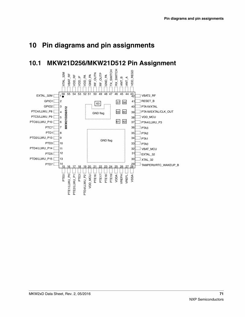
Pin diagrams and pin assignments
10.1 MKW21D256/MKW21D512 Pin Assignment
1
2
3
4
5
6
7
8
9
10
11
12
13
14
42
41
40
39
38
37
36
35
34
33
32
31
30
29
56 55 54 53 52 51 50 49 48 47 46 45 44 43
15 16 17 18 19 20 21 22 23 24 25 26 27 28
MK
W21
D25
6/51
2
EXTAL_32M
GPIO1
GPIO2
PTC4/LLWU_P8
PTC5/LLWU_P9
PTC6/LLWU_P10
PTC7
PTD1
PTD2/LLWU_P13
PTD3
PTD4/LLWU_P14
PTD5
PTD6/LLWU_P15
PTD7
63 57 58
6059
61 62
GND flag
GND flag
VBAT2_RF
RESET_B
PTA19/XTAL
PTA18/EXTAL/CLK_OUT
VDD_MCU
PTA4/LLWU_P3
PTA3
PTA2
PTA1
PTA0
VBAT_MCU
EXTAL_32
XTAL_32
TAMPER0/RTC_WAKEUP_B
PT
E0
PT
E1/
LLW
U_P
0
PT
E2/
LLW
U_P
1
PT
E3
PT
E4/
LLW
U_P
2
VD
D_M
CU
PT
E16
PT
E17
PT
E18
PT
E19
VD
DA
VR
EF
H
VR
EF
L
VS
SA
XTA
L_32
M
VB
AT_R
F
VD
D_R
F
VD
D_I
F
VD
D_P
A
GN
D_P
A
RF
_OU
TN
RF
_OU
TP
GN
D_P
A
TX
_SW
ITC
H
RX
_SW
ITC
H
AN
T_B
AN
T_A
VD
D_R
EG
D
10
Pin diagrams and pin assignments
MKW2xD Data Sheet, Rev. 2, 05/2016 71
NXP Semiconductors

10.2 MKW22/24D512V Pin Assignment
1
2
3
4
5
6
7
8
9
10
11
12
13
14
42
41
40
39
38
37
36
35
34
33
32
31
30
29
56 55 54 53 52 51 50 49 48 47 46 45 44 43
15 16 17 18 19 20 21 22 23 24 25 26 27 28
MK
W22
/24D
512
(US
B)
EXTAL_32M
GPIO1
GPIO2
PTC4/LLWU_P8
PTC5/LLWU_P9
PTC6/LLWU_P10
PTC7
PTD1
PTD2/LLWU_P13
PTD3
PTD4/LLWU_P14
PTD5
PTD6/LLWU_P15
PTD7
63 57 58
6059
61 62
GND flag
GND flag
VBAT2_RF
RESET_B
PTA19/XTAL
PTA18/EXTAL/CLK_OUT
VDD_MCU
PTA4/LLWU_P3
PTA3
PTA2
PTA1
PTA0
VBAT_MCU
EXTAL_32
XTAL_32
TAMPER0/RTC_WAKEUP_B
PT
E0
PT
E1/
LLW
U_P
0
PT
E2/
LLW
U_P
1
PT
E3
PT
E4/
LLW
U_P
2
VD
D_M
CU
US
B0_
DP
US
B0_
DM
VO
UT
33
VR
EG
IN
VD
DA
VR
EF
H
VR
EF
L
VS
SA
XTA
L_32
M
VB
AT_R
F
VD
D_R
F
VD
D_I
F
VD
D_P
A
GN
D_P
A
RF
_OU
TN
RF
_OU
TP
GN
D_P
A
TX
_SW
ITC
H
RX
_SW
ITC
H
AN
T_B
AN
T_A
VD
D_R
EG
D
10.3 Pin assignments
Note
SPI1 (ALT2): SPI1 is dedicated to the radio and is not analternate MCU peripheral.
Table 48. Pin Assignments
MKW22/24D512(USB)
MKW21D256/512
PinName
Default ALT0 ALT1 ALT2 ALT3 ALT4 ALT5 ALT6 ALT7EZPO
RT
1 1 EXTAL_32M
EXTAL_32M
2 2 GPIO1 GPIO1
3 3 GPIO2 GPIO2
Table continues on the next page...
Pin diagrams and pin assignments
72 MKW2xD Data Sheet, Rev. 2, 05/2016
NXP Semiconductors

Table 48. Pin Assignments (continued)
MKW22/24D512(USB)
MKW21D256/512
PinName
Default ALT0 ALT1 ALT2 ALT3 ALT4 ALT5 ALT6 ALT7EZPO
RT
4 4 PTC4/LLWU_
P8
Disabled PTC4/LLWU_
P8
SPI0_PCS0
UART1_TX
FTM0_CH3
CMP1_OUT
5 5 PTC5/LLWU_
P9
Disabled PTC5/LLWU_
P9
SPI0_SCK
LPTMR0_AL
T2
I2S0_RXD0
CMP0_OUT
6 6 PTC6/LLWU_
P10
CMP0_IN0 CMP0_IN0
PTC6/LLWU_
P10
SPI0_SOUT
PDB0_EXTR
G
I2S0_RX_BCL
K
I2S0_MCLK
7 7 PTC7 CMP0_IN1 CMP0_IN1
PTC7 SPI0_SIN
USB_SOF_O
UT
I2S0_RX_FS
8 8 PTD1 ADC0_SE5b ADC0_SE5b
PTD1 SPI0_SCK
UART2_CTS_
b
9 9 PTD2/LLWU_
P13
Disabled PTD2/LLWU_
P13
SPI0_SOUT
UART2_RX
I2C0_SCL
10 10 PTD3 Disabled PTD3 SPI0_SIN
UART2_TX
I2C0_SDA
11 11 PTD4/LLWU_
P14
ADC0_SE21 ADC0_SE21
PTD4/LLWU_
P14
SPI0_PCS1
UART0_RTS_
b
FTM0_CH4
EWM_IN
12 12 PTD5 ADC0_SE6b ADC0_SE6b
PTD5 SPI0_PCS2
UART0_CTS_
b/UART0_COL_
b
FTM0_CH5
EWM_OUT_b
13 13 PTD6/LLWU_
P15
ADC0_SE7b ADC0_SE7b
PTD6/LLWU_
P15
SPI0_PCS3
UART0_RX
FTM0_CH6
FTM0_FLT0
14 14 PTD7 ADC0_SE22 ADC0_SE22
PTD7 CMT_IRO
UART0_TX
FTM0_CH7
FTM0_FLT1
15 15 PTE0 ADC0_SE10 ADC0_SE10
PTE0 SPI1_PCS1
UART1_TX
TRACE_CLKOUT
I2C1_SDA
RTC_CLKOUT
16 16 PTE1/LLWU_
P0
DC0_SE11 ADC0_SE11
PTE1/LLWU_
P0
SPI1_SOUT
UART1_RX
TRACE_D3
I2C1_SCL
SPI1_SIN
17 17 PTE2/LLWU_
P1
ADC0_DP1 ADC0_DP1
PTE2/LLWU_
P1
SPI1_SCK
UART1_CTS_
b
TRACE_D2
Table continues on the next page...
Pin diagrams and pin assignments
MKW2xD Data Sheet, Rev. 2, 05/2016 73
NXP Semiconductors

Table 48. Pin Assignments (continued)
MKW22/24D512(USB)
MKW21D256/512
PinName
Default ALT0 ALT1 ALT2 ALT3 ALT4 ALT5 ALT6 ALT7EZPO
RT
18 18 PTE3 ADC0_DM1 ADC0_DM1
PTE3 SPI1_SIN
UART1_RTS_
b
TRACE_D1
SPI1_SOUT
19 19 PTE4/LLWU_
P2
Disabled PTE4/LLWU_
P2
SPI1_PCS0
TRACE_D0
20 20 VDD_MCU
VDD
21 PTE16 ADC0_SE4a ADC0_SE4a
PTE16 SPI0_PCS0
UART2_TX
FTM_CLKIN0
FTM0_FLT3
22 PTE17 ADC0_SE5a ADC0_SE5a
PTE17 SPI0_SCK
UART2_RX
FTM_CLKIN1
LPTMR0_AL
T3
23 PTE18 ADC0_SE6a ADC0_SE6a
PTE18 SPI0_SOUT
UART2_CTS_
b
I2C0_SDA
24 PTE19 ADC0_SE7a ADC0_SE7a
PTE19 SPI0_SIN
UART2_RTS_
b
I2C0_SCL
21 USB0_DP
USB0_DP USB0_DP
22 USB0_DM
USB0_DM USB0_DM
23 VOUT33
VOUT33 VOUT33
24 VREGIN
VREGIN VREGIN
25 25 VDDA VDDA VDDA
26 26 VREFH VREFH VREFH
27 27 VREFL VREFL VREFL
28 28 VSSA VSSA VSSA
29 29 TAMPER0/
RTC_WAKEUP_B
TAMPER0/RTC_WAKEUP_B
TAMPER0/RTC_WAKEUP_B
30 30 XTAL32
XTAL32 XTAL32
31 31 EXTAL32
EXTAL32 EXTAL32
32 32 VBAT_MCU
VBAT_MCU VBAT_MCU
Table continues on the next page...
Pin diagrams and pin assignments
74 MKW2xD Data Sheet, Rev. 2, 05/2016
NXP Semiconductors

Table 48. Pin Assignments (continued)
MKW22/24D512(USB)
MKW21D256/512
PinName
Default ALT0 ALT1 ALT2 ALT3 ALT4 ALT5 ALT6 ALT7EZPO
RT
33 33 PTA0 JTAG_TCLK/SWD_CLK/EZP_CLK
PTA0 UART0_CTS_
b/UART0_COL_
b
FTM0_CH5
JTAG_TCLK/SWD_CLK
EZP_CLK
34 34 PTA1 JTAG_TDI/EZP_DI
PTA1 UART0_RX
FTM0_CH6
JTAG_TDI
EZP_DI
35 35 PTA2 JTAG_TDO/TRACE_SWO/
EZP_DO
PTA2 UART0_TX
FTM0_CH7
JTAG_TDO/TRACE_SW
O
EZP_DO
36 36 PTA3 JTAG_TMS/SWD_DIO
PTA3 UART0_RTS_
b
FTM0_CH0
JTAG_TMS/SWD_DIO
37 37 PTA4/LLWU_
P3
NMI_b/EZP_CS_b PTA4/LLWU_
P3
FTM0_CH1
NMI_b EZP_CS_b
38 38 VDD2_MCU
VDD VDD
39 39 PTA18 EXTAL0 EXTAL0
PTA18 FTM0_FLT2
FTM_CLKIN0
40 40 PTA19 XTAL0 XTAL0 PTA19 FTM1_FLT0
FTM_CLKIN1
LPTMR0_AL
T1
41 41 RESET_b
RESET_b RESET_b
42 42 VBAT2_RF
VBAT2_RF
431 431 VDD_REGD
VDD_REGD
44 44 ANT_A ANT_A
45 45 ANT_B ANT_B
46 46 RX_SWITCH
RX_SWITCH
47 47 TX_SWITCH
TX_SWITCH
48 48 GND_PA
VSSA_PA
49 49 RF_OUTP
RF_OUTP
Table continues on the next page...
Pin diagrams and pin assignments
MKW2xD Data Sheet, Rev. 2, 05/2016 75
NXP Semiconductors

Table 48. Pin Assignments (continued)
MKW22/24D512(USB)
MKW21D256/512
PinName
Default ALT0 ALT1 ALT2 ALT3 ALT4 ALT5 ALT6 ALT7EZPO
RT
50 50 RF_OUTN
RF_OUTN
51 51 GND_PA
VSSA_PA
521 521 VDD_PA
VDD_PA
531 531 VDD_IF
VDD_IF
541 541 VDD_RF
VDD_RF
55 55 VBAT_RF
VBAT
56 56 XTAL_32M
XTAL_32M
57 57 Factorytest
Do not connect
58 58 Factorytest
Do not connect
59 59 Factorytest
Do not connect
60 60 Factorytest
Do not connect
61 61 Factorytest
Do not connect
62 62 Factorytest
Do not connect
63 63 GND_PA
Connect to ground
1. This pin is used for external bypassing of an internal regulator. DO NOT connect to power.
11 Dimensions
11.1 Obtaining package dimensions
Package dimensions are provided in package drawings.
To find a package drawing, go to nxp.com and perform a keyword search for thedrawing’s document number:
Dimensions
76 MKW2xD Data Sheet, Rev. 2, 05/2016
NXP Semiconductors
If you want the drawing for this package Then use this document number
63 MAPLGA 98ASA00393D
12 Revision HistoryThe following table provides a revision history for this document.
Table 49. Revision History
Rev. No. Date Substantial Changes
2 05/2016 • Updated features list and added pin package diagram on frontpage.
• Added Related Resources table.• Updated structure of section 4 and added section 4.5 "RF Output
Power Distribution".• Added section 5.1 "Transceiver Transmit Current Distribution".• Updated pin diagrams with correct pin assignments.• Replaced MKW2x with MKW2xD through out.
Revision History
MKW2xD Data Sheet, Rev. 2, 05/2016 77
NXP Semiconductors

How to Reach Us:
Home Page:nxp.com
Web Support:nxp.com/support
Information in this document is provided solely to enable system and softwareimplementers to use NXP products. There are no express or implied copyrightlicenses granted hereunder to design or fabricate any integrated circuits basedon the information in this document. NXP reserves the right to make changeswithout further notice to any products herein.
NXP makes no warranty, representation, or guarantee regarding the suitability ofits products for any particular purpose, nor does NXP assume any liability arisingout of the application or use of any product or circuit, and specifically disclaimsany and all liability, including without limitation consequential or incidentaldamages. “Typical” parameters that may be provided in NXP data sheets and/orspecifications can and do vary in different applications, and actual performancemay vary over time. All operating parameters, including “typicals,” must bevalidated for each customer application by customerʼs technical experts. NXPdoes not convey any license under its patent rights nor the rights of others. NXPsells products pursuant to standard terms and conditions of sale, which can befound at the following address: nxp.com/SalesTermsandConditions.
NXP, the NXP logo, NXP SECURE CONNECTIONS FOR A SMARTERWORLD, Freescale, the Freescale logo, and Kinetis are trademarks of NXP B.V.All other product or service names are the property of their respective owners.ARM, the ARM powered logo, and Cortex are registered trademarks of ARMLimited (or its subsidiaries) in the EU and/or elsewhere. All rights reserved.
© 2013 - 2016 NXP B.V.
Document Number MKW2xDxxxRevision 2, 05/2016