Mixed-Mode Baseband for 100 Gbit/s Wireless Communication
32
WS-03 | Wireless 100Gb/s and Beyond: Progress in Ultra-fast Wireless Communications European Microwave Week 2017 EuMC Mixed-Mode Baseband for 100 Gbit/s Wireless Communication J. Christoph Scheytt 1 , Rolf Kraemer 2 , Ingmar Kallfass 3 [email protected] 1 Heinz Nixdorf Institute, University of Paderborn, 2 BTU Cottbus-Senftenberg, 3 University of Stuttgart
Transcript of Mixed-Mode Baseband for 100 Gbit/s Wireless Communication
WS-03 | Wireless 100Gb/s and Beyond: Progress in Ultra-fast Wireless Communications
European Microwave Week 2017 EuMC
Mixed-Mode Baseband for 100 Gbit/s Wireless Communication
J. Christoph Scheytt1, Rolf Kraemer2, Ingmar Kallfass3
1Heinz Nixdorf Institute, University of Paderborn, 2BTU Cottbus-Senftenberg, 3University of Stuttgart
WS-03 | Wireless 100Gb/s and Beyond: Progress in Ultra-fast Wireless Communications
European Microwave Week 2017 EuMC Slide 2
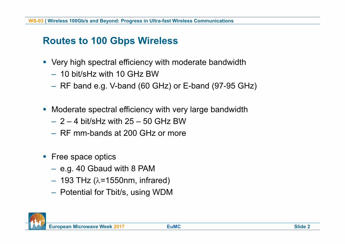
Very high spectral efficiency with moderate bandwidth– 10 bit/sHz with 10 GHz BW– RF band e.g. V-band (60 GHz) or E-band (97-95 GHz)
Moderate spectral efficiency with very large bandwidth– 2 – 4 bit/sHz with 25 – 50 GHz BW– RF mm-bands at 200 GHz or more
Free space optics– e.g. 40 Gbaud with 8 PAM – 193 THz (=1550nm, infrared) – Potential for Tbit/s, using WDM
Routes to 100 Gbps Wireless
WS-03 | Wireless 100Gb/s and Beyond: Progress in Ultra-fast Wireless Communications
European Microwave Week 2017 EuMC Slide 3
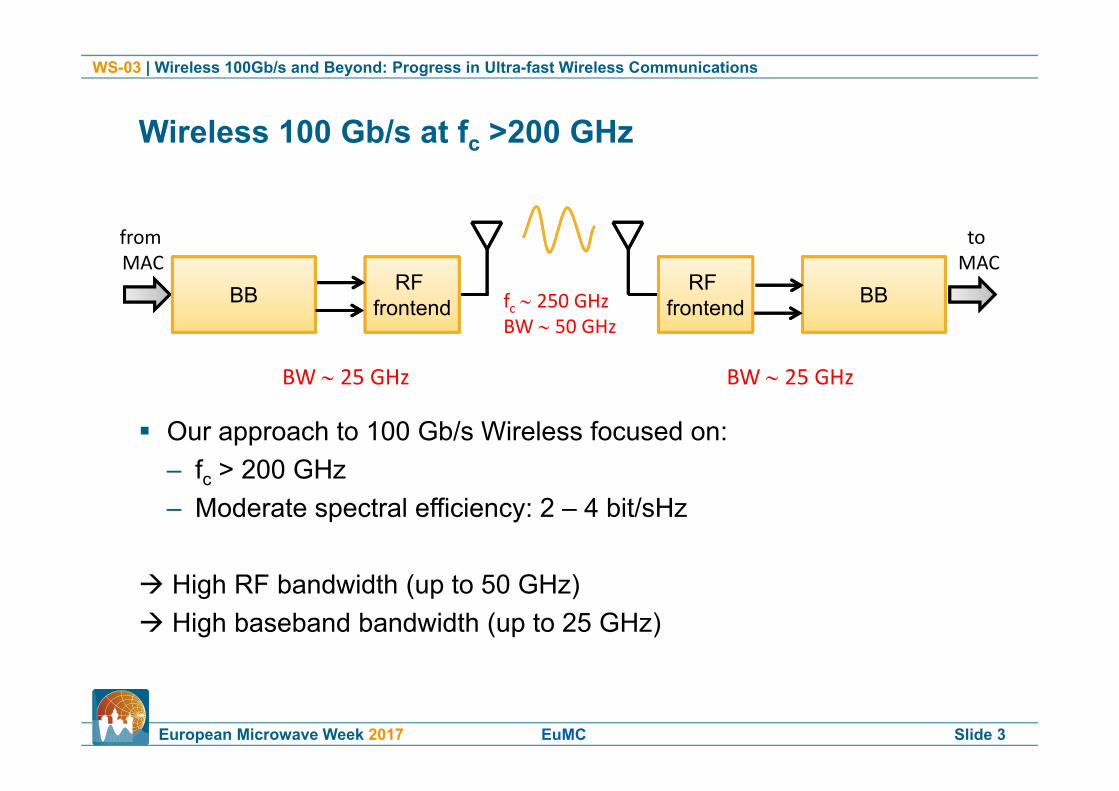
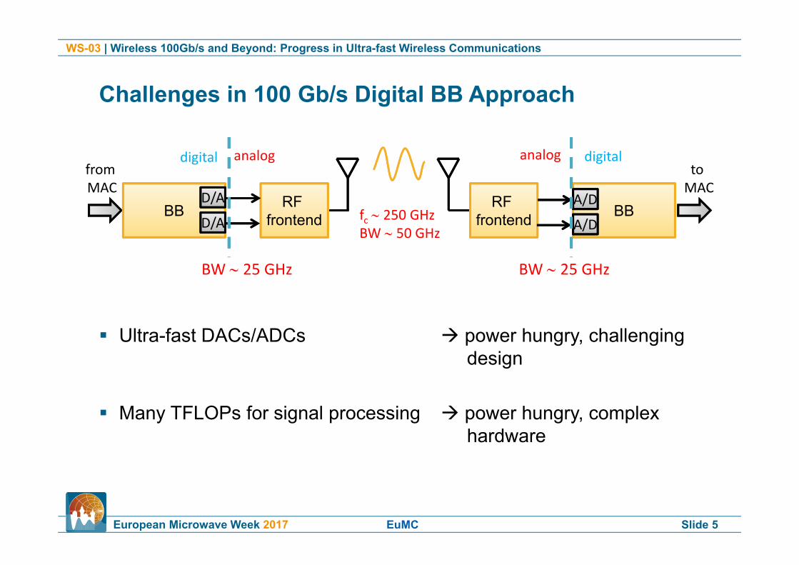
Our approach to 100 Gb/s Wireless focused on: – fc > 200 GHz– Moderate spectral efficiency: 2 – 4 bit/sHz
High RF bandwidth (up to 50 GHz) High baseband bandwidth (up to 25 GHz)
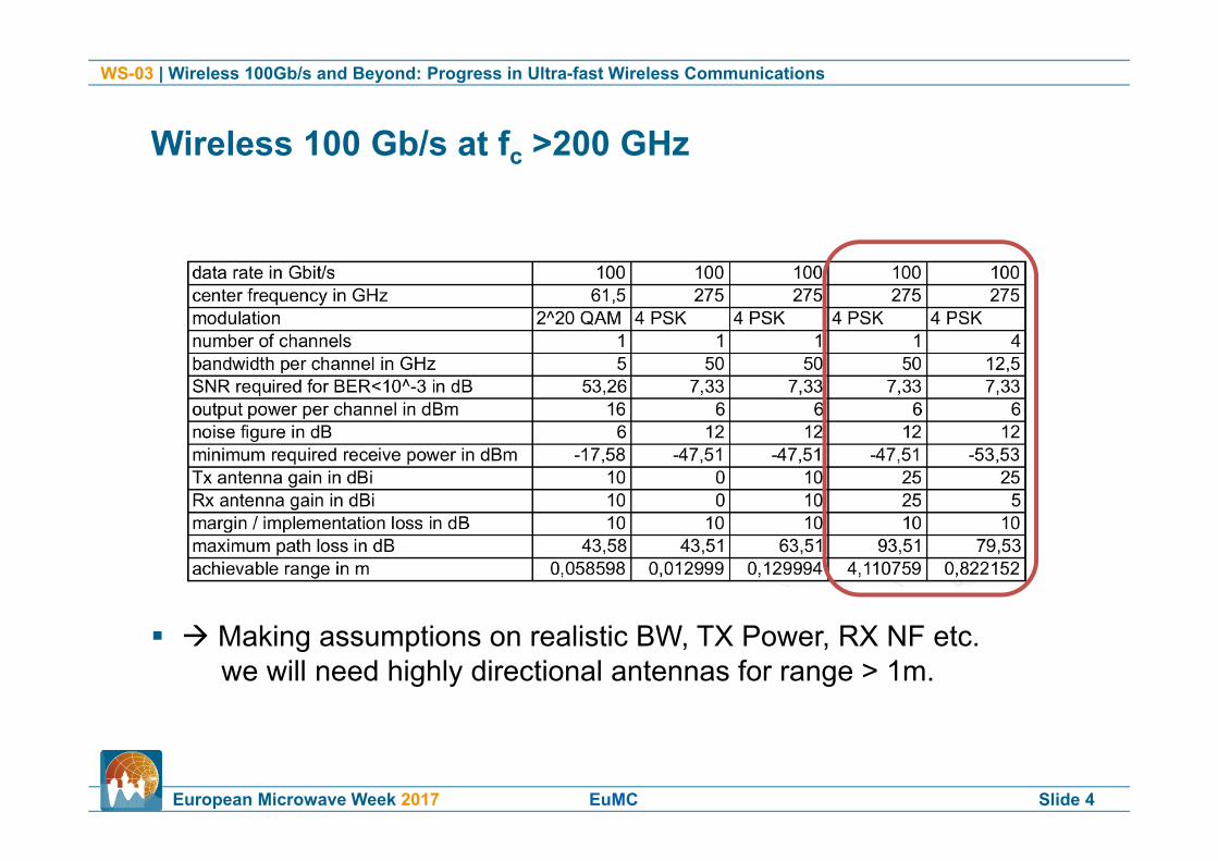
Wireless 100 Gb/s at fc >200 GHz
RF frontend
BW 25 GHz
toMAC
BBRF frontend
BW 25 GHz
fromMAC
BB fc 250 GHz BW 50 GHz
WS-03 | Wireless 100Gb/s and Beyond: Progress in Ultra-fast Wireless Communications
European Microwave Week 2017 EuMC Slide 4
Making assumptions on realistic BW, TX Power, RX NF etc. we will need highly directional antennas for range > 1m.
Wireless 100 Gb/s at fc >200 GHz
WS-03 | Wireless 100Gb/s and Beyond: Progress in Ultra-fast Wireless Communications
European Microwave Week 2017 EuMC Slide 5
Ultra-fast DACs/ADCs power hungry, challenging design
Many TFLOPs for signal processing power hungry, complex hardware
Challenges in 100 Gb/s Digital BB Approach
RF frontend
BW 25 GHz
toMAC
BBRF frontend
BW 25 GHz
fromMAC
BB fc 250 GHz BW 50 GHz
analogdigital
D/A
D/AA/D
A/D
analog digital

WS-03 | Wireless 100Gb/s and Beyond: Progress in Ultra-fast Wireless Communications
European Microwave Week 2017 EuMC Slide 8
Analog processing is inherently power and hardware-efficient, especially for broadband circuits.
Shift analog/digital boundary mixed-signal BB with significant analog processing
„Analog-friendly“ modulation Parallel Spread-Spectrum Seq. (PSSS)
Efficient synchronisation Coherent detection in analog/RF domain
100 Gb/s Mixed-Signal BB Approach
RF frontend
BW 25 GHz
toMAC
BB RF frontend
BW 25 GHz
fromMAC
BB fc 250 GHz BW 50 GHz
analogdigital
D/A
D/AA/D
A/D
analog digital
WS-03 | Wireless 100Gb/s and Beyond: Progress in Ultra-fast Wireless Communications
European Microwave Week 2017 EuMC Slide 9
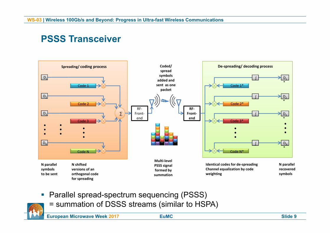
Parallel spread-spectrum sequencing (PSSS) = summation of DSSS streams (similar to HSPA)
PSSS Transceiver
N parallel symbols to be sent
N shifted versions of an orthogonal code for spreading
Multi‐level PSSS signal formed by summation
Spreading/ coding process Coded/spread symbolsadded and sent as one
packet
De‐spreading/ decoding process
N parallel recovered symbols
Code 1
Code 2
Code 3
Code N
∑
Code 1*
Code 2*
Code 3*
Code N*
Identical codes for de‐spreadingChannel equalization by code weighting
D1
D2
D3
DN
D2*
D3*
DN*
D1*
∫
∫
∫
∫
RF‐Front‐end
RF‐Front‐end

WS-03 | Wireless 100Gb/s and Beyond: Progress in Ultra-fast Wireless Communications
European Microwave Week 2017 EuMC Slide 10
Significant part of PSSS BB processing in analog/mixed-signal domain Low-speed DACs and ADCs operate at symbol rate.
PSSS Transceiver
N parallel symbols to be sent
N shifted versions of an orthogonal code for spreading
Multi‐level PSSS signal formed by summation
Spreading/ coding process Coded/spread symbolsadded and sent as one
packet
De‐spreading/ decoding process
N parallel recovered symbols
Code 1
Code 2
Code 3
Code N
∑
Code 1*
Code 2*
Code 3*
Code N*
Identical codes for de‐spreadingChannel equalization by code weighting
D1
D2
D3
DN
D2*
D3*
DN*
D1*
∫
∫
∫
∫
RF‐Front‐end
RF‐Front‐end
analogdigital analog digital
WS-03 | Wireless 100Gb/s and Beyond: Progress in Ultra-fast Wireless Communications
European Microwave Week 2017 EuMC Slide 11
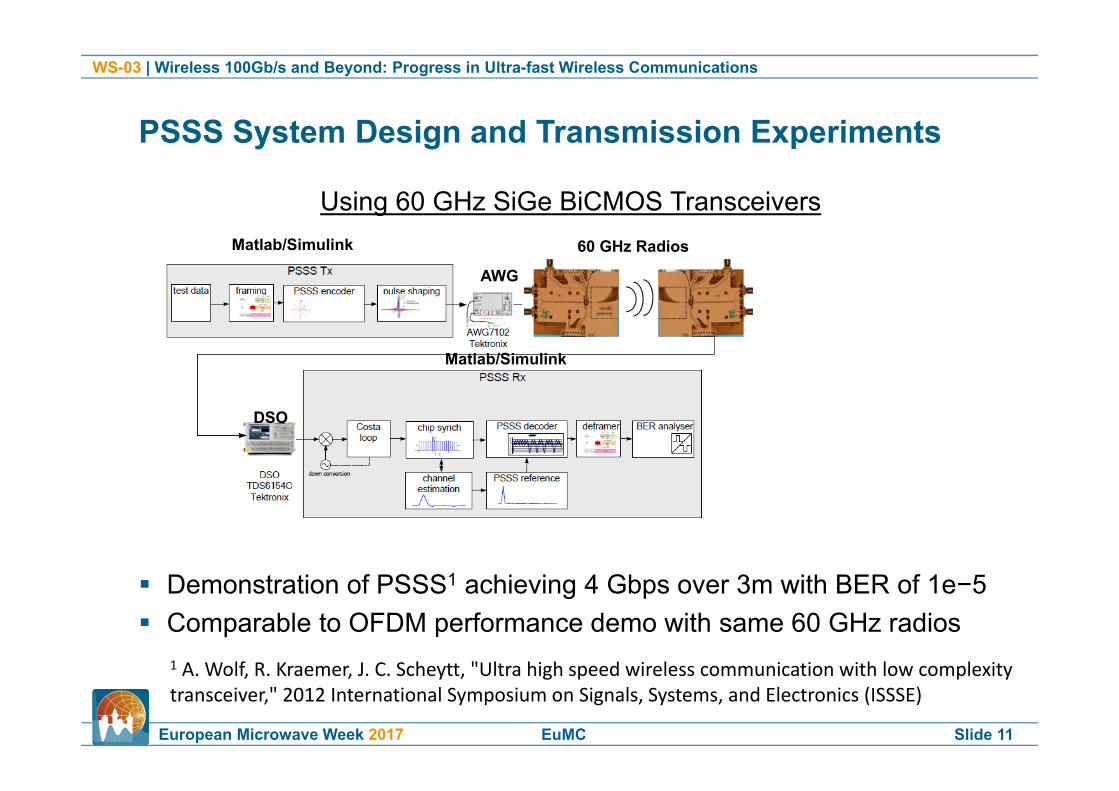
Using 60 GHz SiGe BiCMOS Transceivers
Demonstration of PSSS1 achieving 4 Gbps over 3m with BER of 1e−5 Comparable to OFDM performance demo with same 60 GHz radios
PSSS System Design and Transmission Experiments
Matlab/Simulink
AWG
DSO
60 GHz Radios
Matlab/Simulink
1 A. Wolf, R. Kraemer, J. C. Scheytt, "Ultra high speed wireless communication with low complexity transceiver," 2012 International Symposium on Signals, Systems, and Electronics (ISSSE)
WS-03 | Wireless 100Gb/s and Beyond: Progress in Ultra-fast Wireless Communications
European Microwave Week 2017 EuMC Slide 12
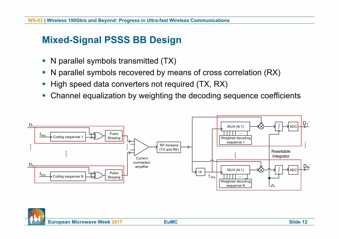
N parallel symbols transmitted (TX) N parallel symbols recovered by means of cross correlation (RX) High speed data converters not required (TX, RX) Channel equalization by weighting the decoding sequence coefficients
Mixed-Signal PSSS BB Design
∫
Current summation
amplifier
….
….…
.
MUX (N:1)
CRC
Weighted decoding sequence 1
...
….
ADC
….
D1´
DN´ ∫ ADC
Resettable Integrator
Coding sequence 1fchip
D1
MUX (N:1)
Weighted decoding sequence N
...
Pulse Shaping
Pulse Shaping
RF frontend(TX and RX)
Coding sequence Nfchip
DN
f´chip
CR
WS-03 | Wireless 100Gb/s and Beyond: Progress in Ultra-fast Wireless Communications
European Microwave Week 2017 EuMC Slide 13
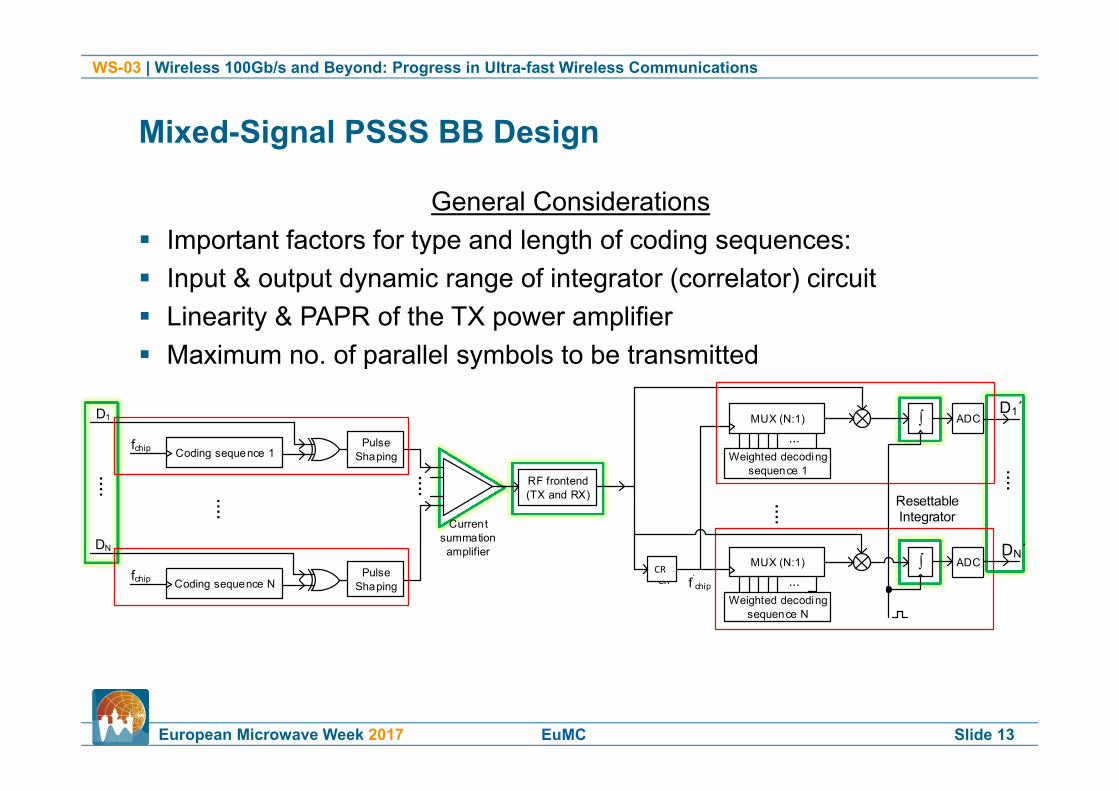
General Considerations Important factors for type and length of coding sequences: Input & output dynamic range of integrator (correlator) circuit Linearity & PAPR of the TX power amplifier Maximum no. of parallel symbols to be transmitted
Mixed-Signal PSSS BB Design
CRCR
∫
Current summation
amplifier
….
….…
.
MUX (N:1)
CRC
Weighted decoding sequence 1
...
….
ADC
….
D1´
DN´ ∫ ADC
Resettable Integrator
Coding sequence 1fchip
D1
MUX (N:1)
Weighted decoding sequence N
...
Pulse Shaping
Pulse Shaping
RF frontend(TX and RX)
Coding sequence Nfchip
DN
f´chip
CR

WS-03 | Wireless 100Gb/s and Beyond: Progress in Ultra-fast Wireless Communications
European Microwave Week 2017 EuMC Slide 14
PSSS Coding Sequences Mixed signal PSSS baseband realization chose shorter coding sequences
Coding sequences considered:– Maximum length sequences (MLS or m-sequences):
length 7, 15, or 31– Barker codes: length 7, 11, 13
MLS-15 turned out to be best choice formixed signal PSSS BB implementation
Mixed-Signal PSSS BB Design1
1 A. R. Javed, C. Scheytt: “System Design Considerations for a PSSS Transceiver for 100Gbps Wireless Communication with Emphasis on Mixed Signal Implementation ”, IEEE WAMICOLN 2015
WS-03 | Wireless 100Gb/s and Beyond: Progress in Ultra-fast Wireless Communications
European Microwave Week 2017 EuMC Slide 15
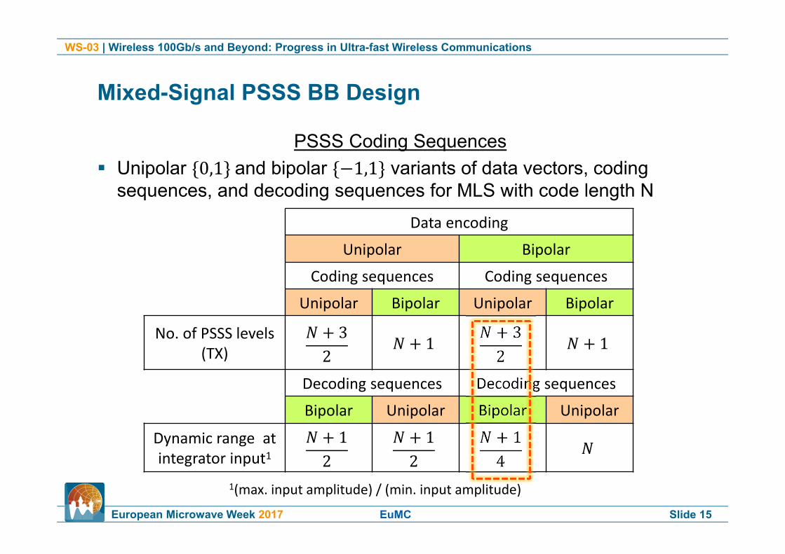
PSSS Coding Sequences Unipolar 0,1 and bipolar 1,1 variants of data vectors, coding
sequences, and decoding sequences for MLS with code length N
Mixed-Signal PSSS BB Design
Data encoding
Unipolar Bipolar
Coding sequences Coding sequences
Unipolar Bipolar Unipolar Bipolar
No. of PSSS levels(TX)
+ 32 + 1 + 32 + 1Decoding sequences Decoding sequences
Bipolar Unipolar Bipolar Unipolar
Dynamic range at integrator input1
+ 12 + 12 + 141(max. input amplitude) / (min. input amplitude)

WS-03 | Wireless 100Gb/s and Beyond: Progress in Ultra-fast Wireless Communications
European Microwave Week 2017 EuMC Slide 16
PSSS Coding Sequences Comparison of MLS-15 with Barker-11 and Barker-13
Mixed-Signal PSSS BB Design
Data (bipolar)
Coding sequences(MLS‐15)
Coding sequences(Barker‐11)
Coding sequences(Barker‐13)
Unipolar Bipolar Unipolar Bipolar Unipolar Bipolar
No. of PSSS levels 9 16 6 12 10 14Decoding sequences Decoding sequences Decoding sequences
Bipolar Unipolar Bipolar+ 0.2*
Unipolar‐1.0*
Bipolar‐0.33*
Unipolar‐0.6*
Dynamic rangeat integrator
input4 15 6 11 12 8
* For barker codes a DC offset is required in the decoding sequence

WS-03 | Wireless 100Gb/s and Beyond: Progress in Ultra-fast Wireless Communications
European Microwave Week 2017 EuMC Slide 17
Chip Rate
Maximum realizable chip rate: 25 30 Gcps (0.13µm BiCMOS)
Minimum bit loading required: 4 since
25 × 4 = 100 sec
Mixed-Signal PSSS BB Design
∫
Current summation
amplifier
….
….…
.
MUX (N:1)
CRC
Weighted decoding sequence 1
...
….
ADC
….
D1´
DN´ ∫ ADC
Resettable Integrator
Coding sequence 1fchip
D1
MUX (N:1)
Weighted decoding sequence N
...
Pulse Shaping
Pulse Shaping
RF frontend(TX and RX)
Coding sequence Nfchip
DN
f´chip
CR
WS-03 | Wireless 100Gb/s and Beyond: Progress in Ultra-fast Wireless Communications
European Microwave Week 2017 EuMC Slide 18
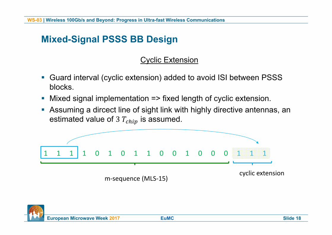
Cyclic Extension
Guard interval (cyclic extension) added to avoid ISI between PSSS blocks.
Mixed signal implementation => fixed length of cyclic extension. Assuming a dircect line of sight link with highly directive antennas, an
estimated value of 3 is assumed.
Mixed-Signal PSSS BB Design
1 1 1 1 0 1 0 1 1 0 0 1 0 0 0 1 1 1
m‐sequence (MLS‐15)cyclic extension
WS-03 | Wireless 100Gb/s and Beyond: Progress in Ultra-fast Wireless Communications
European Microwave Week 2017 EuMC Slide 19
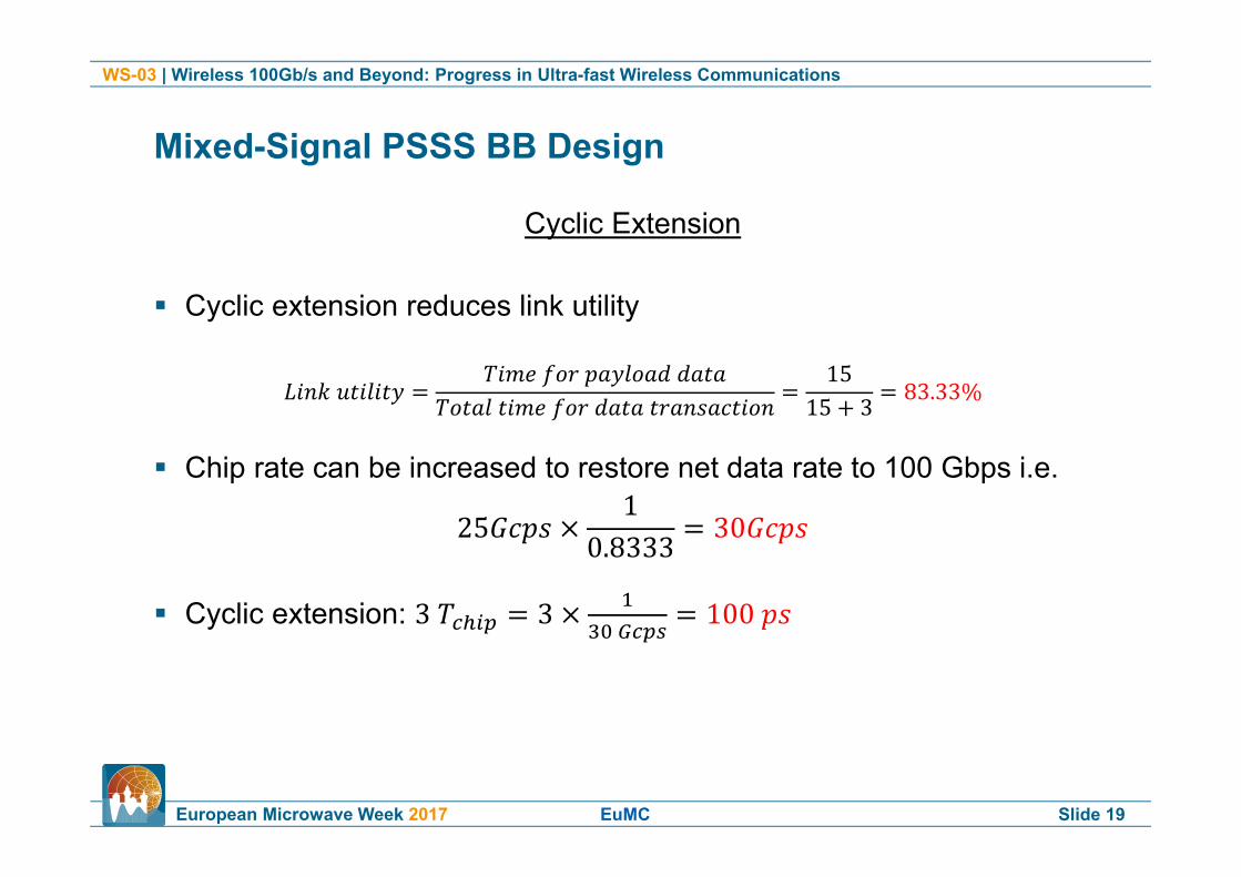
Cyclic Extension
Cyclic extension reduces link utility
= = 1515 + 3 = 83.33% Chip rate can be increased to restore net data rate to 100 Gbps i.e.25 × 10.8333 = 30 Cyclic extension: 3 = 3 × = 100
Mixed-Signal PSSS BB Design
WS-03 | Wireless 100Gb/s and Beyond: Progress in Ultra-fast Wireless Communications
European Microwave Week 2017 EuMC Slide 20
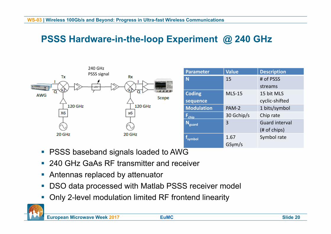
PSSS baseband signals loaded to AWG 240 GHz GaAs RF transmitter and receiver Antennas replaced by attenuator DSO data processed with Matlab PSSS receiver model Only 2-level modulation limited RF frontend linearity
PSSS Hardware-in-the-loop Experiment @ 240 GHz
Parameter Value DescriptionN 15 # of PSSS
streamsCodingsequence
MLS‐15 15 bit MLS cyclic‐shifted
Modulation PAM‐2 1 bits/symbol Fchip 30 Gchip/s Chip rateNguard 3 Guard interval
(# of chips)fsymbol 1.67
GSym/sSymbol rate
240 GHzPSSS signal
WS-03 | Wireless 100Gb/s and Beyond: Progress in Ultra-fast Wireless Communications
European Microwave Week 2017 EuMC Slide 21
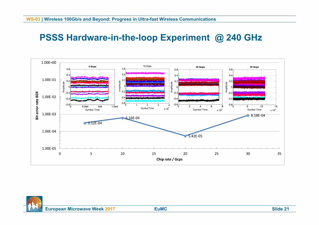
PSSS Hardware-in-the-loop Experiment @ 240 GHz

WS-03 | Wireless 100Gb/s and Beyond: Progress in Ultra-fast Wireless Communications
European Microwave Week 2017 EuMC Slide 22
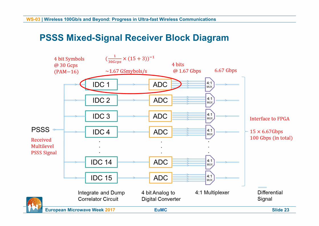
PSSS Mixed-Signal Receiver Block Diagram
WS-03 | Wireless 100Gb/s and Beyond: Progress in Ultra-fast Wireless Communications
European Microwave Week 2017 EuMC Slide 23
PSSS Mixed-Signal Receiver Block Diagram
WS-03 | Wireless 100Gb/s and Beyond: Progress in Ultra-fast Wireless Communications
European Microwave Week 2017 EuMC Slide 24
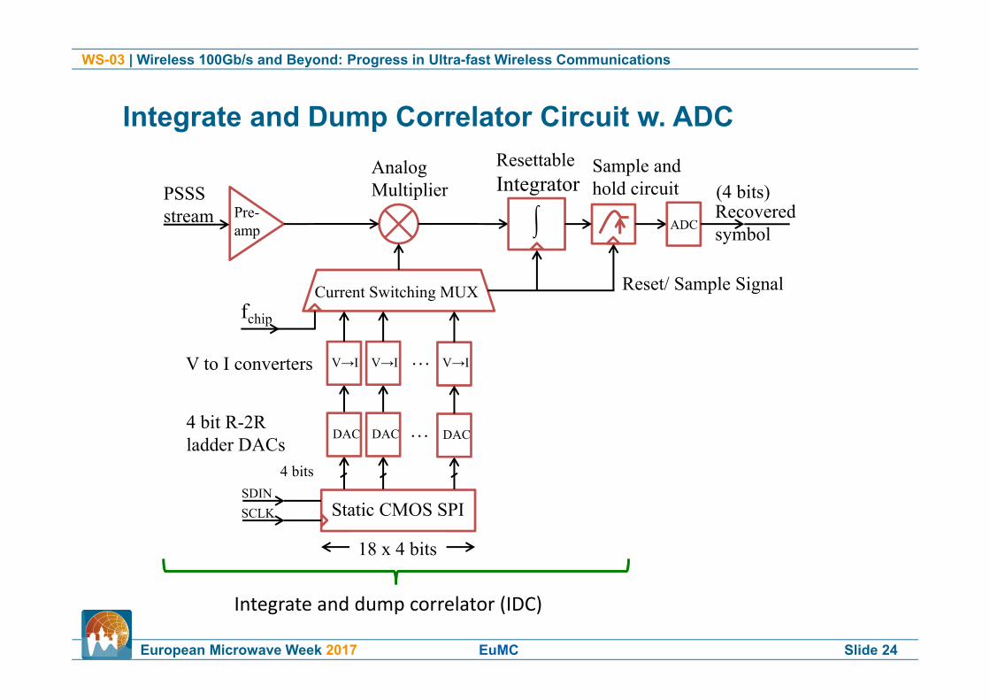
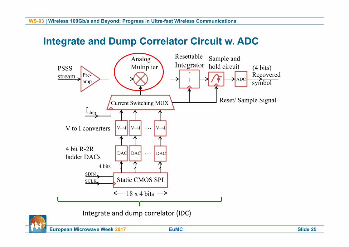
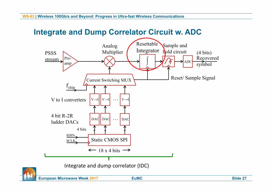
Integrate and Dump Correlator Circuit w. ADC
PSSS stream
V to I converters
Static CMOS SPI
…
…
Current Switching MUX
Sample and hold circuit
Pre-amp
Analog Multiplier
ResettableIntegrator
Reset/ Sample Signal
4 bit R-2R ladder DACs
DAC DAC DAC
4 bits
V→I V→I V→I
fchip
SDINSCLK
RecoveredsymbolADC
(4 bits)
Integrate and dump correlator (IDC)
18 x 4 bits
WS-03 | Wireless 100Gb/s and Beyond: Progress in Ultra-fast Wireless Communications
European Microwave Week 2017 EuMC Slide 25
Integrate and Dump Correlator Circuit w. ADC
PSSS stream
V to I converters
Static CMOS SPI
…
…
Current Switching MUX
Sample and hold circuit
Pre-amp
Analog Multiplier
ResettableIntegrator
Reset/ Sample Signal
4 bit R-2R ladder DACs
DAC DAC DAC
4 bits
V→I V→I V→I
fchip
SDINSCLK
RecoveredsymbolADC
(4 bits)
Integrate and dump correlator (IDC)
18 x 4 bits
WS-03 | Wireless 100Gb/s and Beyond: Progress in Ultra-fast Wireless Communications
European Microwave Week 2017 EuMC Slide 26
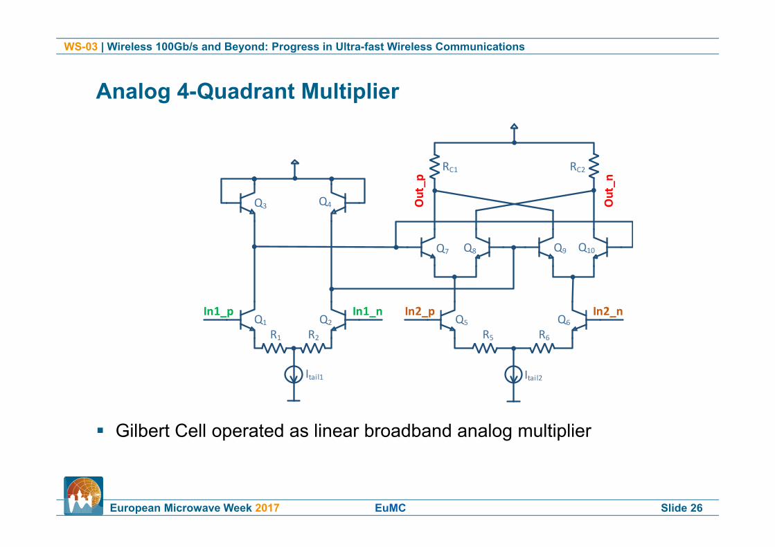
Analog 4-Quadrant Multiplier
Q5
R5
Q6
R6
Itail2
Q7 Q8 Q9 Q10
RC1 RC2
Q1
R1
Q2
R2
Itail1
Q3 Q4
In1_p In1_n In2_p In2_n
Out_p
Out_n
+1.3 V
‐4.0 V
Gilbert Cell operated as linear broadband analog multiplier
WS-03 | Wireless 100Gb/s and Beyond: Progress in Ultra-fast Wireless Communications
European Microwave Week 2017 EuMC Slide 27
Integrate and Dump Correlator Circuit w. ADC
PSSS stream
V to I converters
Static CMOS SPI
…
…
Current Switching MUX
Sample and hold circuit
Pre-amp
Analog Multiplier
ResettableIntegrator
Reset/ Sample Signal
4 bit R-2R ladder DACs
DAC DAC DAC
4 bits
V→I V→I V→I
fchip
SDINSCLK
RecoveredsymbolADC
(4 bits)
Integrate and dump correlator (IDC)
18 x 4 bits
WS-03 | Wireless 100Gb/s and Beyond: Progress in Ultra-fast Wireless Communications
European Microwave Week 2017 EuMC Slide 28
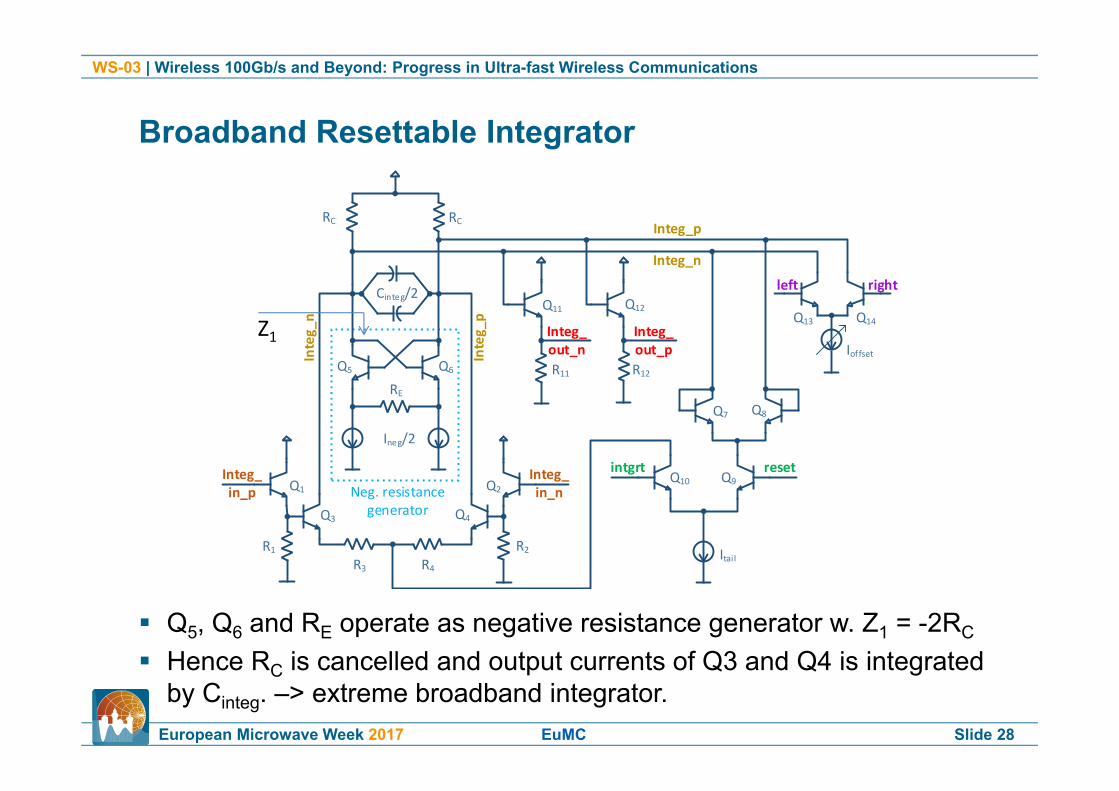
Broadband Resettable Integrator
Q3
R3
Q4
R4
Q1 Q2
R1
Q6Q5
RE
Ineg/2
Cinteg/2
RC1 RC2
Integ_in_p
Integ_in_n
Integ_n
Integ_p
Neg. resistance generator
Q10 Q9
Itail
intgrt reset
Q7 Q8
R2
Integ_p
Integ_n
Q11
R11
Q12
R12
Integ_out_n
Integ_out_p Ioffset
Q13 Q14
left right
+1.3 V
‐4.0 V
Q5, Q6 and RE operate as negative resistance generator w. Z1 = -2RC
Hence RC is cancelled and output currents of Q3 and Q4 is integratedby Cinteg. –> extreme broadband integrator.
Z1

WS-03 | Wireless 100Gb/s and Beyond: Progress in Ultra-fast Wireless Communications
European Microwave Week 2017 EuMC Slide 29
Broadband Resettable Integrator
Q3
R3
Q4
R4
Q1 Q2
R1
Q6Q5
RE
Ineg/2
Cinteg/2
RC1 RC2
Integ_in_p
Integ_in_n
Integ_n
Integ_p
Neg. resistance generator
Q10 Q9
Itail
intgrt reset
Q7 Q8
R2
Integ_p
Integ_n
Q11
R11
Q12
R12
Integ_out_n
Integ_out_p Ioffset
Q13 Q14
left right
+1.3 V
‐4.0 V
Q3, R3 Q4, R4 represent linear V-I converters Q9, Q10 control integrate and reset phase Q13, Q14 , Ioffset implement integrator offset control
Z1

WS-03 | Wireless 100Gb/s and Beyond: Progress in Ultra-fast Wireless Communications
European Microwave Week 2017 EuMC Slide 30
Broadband Resettable Correlator Test Chip1
1 A. R. Javed, C. Scheytt, U. v.d. Ahe: “Linear Ultra‐Broadband NPN‐only Analog Correlator at 33 Gbps in 130 nm SiGe BiCMOS Technology”, IEEE BCTM 2016
Realized in 130 nm SiGe BiCMOS technology (SG13S) from IHP Measurement results show integrator step response and reset. Correlator with highest input bandwidth (>25 GHz) and smallest reset
time (<130 ps) reported so far.

WS-03 | Wireless 100Gb/s and Beyond: Progress in Ultra-fast Wireless Communications
European Microwave Week 2017 EuMC Slide 31
Integrate and Dump Correlator Circuit w. ADC
PSSS stream
V to I converters
Static CMOS SPI
…
…
Current Switching MUX
Sample and hold circuit
Pre-amp
Analog Multiplier
ResettableIntegrator
Reset/ Sample Signal
4 bit R-2R ladder DACs
DAC DAC DAC
4 bits
V→I V→I V→I
fchip
SDINSCLK
RecoveredsymbolADC
(4 bits)
Integrate and dump correlator (IDC)
18 x 4 bits
Switched Emitter‐FollowerTrack‐and‐Hold1
1 similar to B. Sedighi, Y. Borokhovych, H. Gustat, C. Scheytt: “Low‐power BiCMOStrack‐and‐hold circuit with reduced signal feedthrough”, IEEE IMS 2012
4‐bit Flash ADC
WS-03 | Wireless 100Gb/s and Beyond: Progress in Ultra-fast Wireless Communications
European Microwave Week 2017 EuMC Slide 32
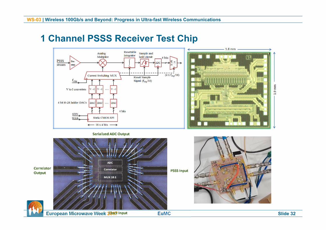
1 Channel PSSS Receiver Test Chip
Integrate and dump correlator (IDC)

WS-03 | Wireless 100Gb/s and Beyond: Progress in Ultra-fast Wireless Communications
European Microwave Week 2017 EuMC Slide 33
Power Dissipation
PSSS stream
V to I converters
Static CMOS SPI
…
…
Current Switching MUX
Sample and hold circuit
Pre-amp
Analog Multiplier
ResettableIntegrator
Reset/ Sample Signal
4 bit R-2R ladder DACs
DAC DAC DAC
4 bits
V→I V→I V→I
fchip
SDINSCLK
RecoveredsymbolADC
(4 bits)
Integrate and dump correlator (IDC)
18 x 4 bits
Component Power diss.
Multiplier 33 mW
Integrator 50 mW
Sample & Hold 22 mW
Signal conditioning and Flash ADC
1 W
Analog MUX 1.9 W
Total (1 Channel) 3.005 W
Circuit implemented in 130 nm SiGe BiCMOS. high BW but not power efficient. Analog Current Switching MUX and Flash ADC most power hungry.
WS-03 | Wireless 100Gb/s and Beyond: Progress in Ultra-fast Wireless Communications
European Microwave Week 2017 EuMC Slide 34
Conclusions
100 Gb/s wireless communication with high RF bandwidth (e.g. 50 GHz) has extreme demand wrt. to baseband data converters and signal processing.
PSSS is an analog-friendly modulation scheme. Mixed-signal PSSS allows for data converters to operate on a fraction of the signal bandwidth and low sampling rate.
Mixed-signal PSSS system design and link experiments were shown.
Circuit design of critical components. Correlator with world‘s highest input bandwidth(>25 GHz) and smallest reset time (<130 ps) was demonstrated.
Implementation in 130nm SiGe BiCMOS shows that a 100 Gb/s mixed-signal PSSS baseband is technically feasible, however not power-efficient.
Power efficient implementation would require a CMOS implementation (at least 45nm) either mixed-signal or digital.