
MIT6_012S09_lec01
23
MIT, Spring 2009 6.012 Microelectronic Devices and Circuits Charles G. Sodini Jing Kong Shaya Famini, Stephanie Hsu, Ming Tang
-
Upload
gopi-krishna -
Category
Documents
-
view
6 -
download
1
description
MIT lectures
Transcript of MIT6_012S09_lec01

MIT, Spring 2009
6.012 Microelectronic Devices and Circuits
Charles G. Sodini
Jing Kong
Shaya Famini, Stephanie Hsu, Ming Tang
This talk is about Si microelectronics. I want to look back to the last 30 years and the explosive progress in integrated circuit technology that has taken place. I also want to look ahead and share with you my sense of how Si microelectronics will continue to surprise us in the years to come.
–
Lecture 1 – 6.012 Overview
• Contents: – Overview of 6.012Overview of 6.012
• Reading Assignment: – Howe and Sodini, Ch. 2

– Com uter revolution
Overview of 6.012
• Introductory subject to microelectronic devices and circuits
• Microelectronics is the cornerstone of: – Computer revolution p
– Communications revolution
– Consumer Electronics revolution

Microelectronics: cornerstone of computing revolution
In last 30 years, computer performance per dollar has improved more than a million fold!
If we were to try to look for a single reason for the widespread popularity of Si microelectronics technology, we should probably have to look into the world of computing. This graph puts in perspective the impact of microelectronics on computing with respect to previous technologies. The graph comes from a very recent book by Raymond Kurzweil titled “The Age of Spiritual Machines.” It graphs a figure of merit for computing that I will describe in a moment along the 20th century. Notice that the figure of merit is graphed on a semilogarithmic scale. The selected figure of merit establishes both the capabilities of computers but also their affordability. It is the number of calculations per second per $1000 worth of computer hardware. The history of computing starts at the beginning of the century with mechanical logic. These were clunky and expensive machines. Progress took place slowly with electromechanical logic, basically relays. Vacuum tube logic got things moving a bit later. These were enormous machines that got very hot and exhibited very poor reliability. The advent of transistor logic reduced the size of computers, increased their reliability, lowered the cost and improved their performance. With the integrated circuit, this progress has exploded. In the last 30 years, since the first ICs were used to build computers, computer performance per dollar cost has improved by over a factor of one million! Just about any personal computer today is more powerful than the most powerful machine of the 1960’s.
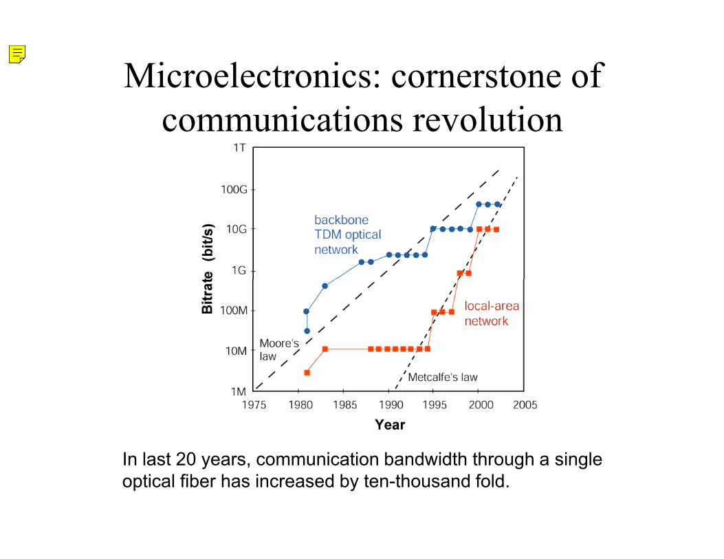
Microelectronics: cornerstone of communications revolution
In last 20 years, communication bandwidth through a single optical fiber has increased by tenthousand fold.
If we were to try to look for a single reason for the widespread popularity of Si microelectronics technology, we should probably have to look into the world of computing. This graph puts in perspective the impact of microelectronics on computing with respect to previous technologies. The graph comes from a very recent book by Raymond Kurzweil titled “The Age of Spiritual Machines.” It graphs a figure of merit for computing that I will describe in a moment along the 20th century. Notice that the figure of merit is graphed on a semilogarithmic scale. The selected figure of merit establishes both the capabilities of computers but also their affordability. It is the number of calculations per second per $1000 worth of computer hardware. The history of computing starts at the beginning of the century with mechanical logic. These were clunky and expensive machines. Progress took place slowly with electromechanical logic, basically relays. Vacuum tube logic got things moving a bit later. These were enormous machines that got very hot and exhibited very poor reliability. The advent of transistor logic reduced the size of computers, increased their reliability, lowered the cost and improved their performance. With the integrated circuit, this progress has exploded. In the last 30 years, since the first ICs were used to build computers, computer performance per dollar cost has improved by over a factor of one million! Just about any personal computer today is more powerful than the most powerful machine of the 1960’s.
Microelectronics: cornerstone of consumer electronics revolution
Low power electronics enabling a variety of portable devices
Images of consumer electronics (cell phones, digital cameras, PDA) removed due to copyright restrictions.

Si digital microelectronics today
Take the cover off a microprocessor. What do you see?
• A thick web of interconnects, many levels deep.many levels deep.
• High density of very small transistors.
Intel’s Pentium IV
Image of Pentium microprocessor removed due to copyright restrictions.
If we take the cover off a modern microprocessor, what do we see? Here is for example a Pentium II from Intel, a workhorse of personal computing today. Modern microchips make nice pictures. If we transcend the beautiful colors and geometrical patterns, we basically see two things. One is a thick web of metallic interconnects. The second thing is a high density of very small transistors.
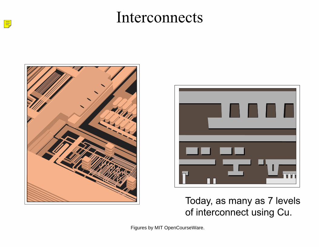
Interconnects
Today, as many as 7 levels of interconnect using Cu.
Figures by MIT OpenCourseWare.
I am not going to spend any significant time in this presentation talking about the interconnects. And that is not because they do not play a key role in integrated circuit design and performance. They do. In fact, there has been a lot of progress in recent years in interconnect technology. We are currently seeing a migration from Al to Cu. The number of levels of interconnect technology is reaching now 7 among the leading companies such as IBM, from where these pictures come. The picture on the left shows the interconnects with the intermetal dielectric removed. It reveals a beautiful scaffolding of copper. The picture on the right shows a cross section across the interconnect layer. It shows one level of local interconnect followed by six levels of Cu-based interconnects. They are all perfectly flat. The surface of the wafer is down here and blown-up is a small transistor. This is where I want to focus now.
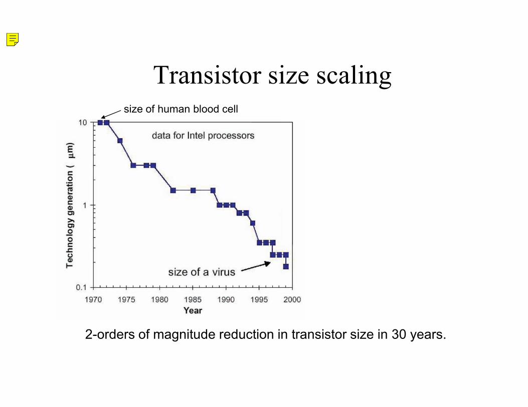
Transistor size scalingsize of human blood cell
2orders of magnitude reduction in transistor size in 30 years.
I want to spend the bulk of my time talking about transistors. Here is a pretty picture of a pair of transistors from an IBM web site. I will discuss later on why they nearly always come in pairs. I will also talk later a bit about the basic operation of the transistor. What I want to focus your attention now is on the relative size of the transistor today. It is very small. When talking about transistor size, we are refering to the length of its gate or controlling element. As I will describe later, this dimension controls many important figures of merit of the transistor. The rest of the transistor dimensions scale with it. Modern transistors have gate lengths of order 0.2-0.3 ?m in size. To put it in perspective, this is the size of a typical virus. In the last 30 years, as this figure shows, this critical dimension has been reduced by two orders of magnitude. This graph shows the gate length of the transistor technology of Intel’s microprocessors since the introduction of its first microprocessor in 1971. There is nothing special about the choice of Intel. Intel’s technology is representative of the overall industry. The length of the gate plays such a critical role that technology progress in this field is often catalogued in “technology generations” that are labeled by the gate length. In this manner, we talk about the 10 ?m generation in the early 80’s, the 1 ?m generation in the mid 80’s, or the 0.35, 0.25 and 0.18 ?m generation of late.
4orders of magnitude
Intel processors
2x/1.5year
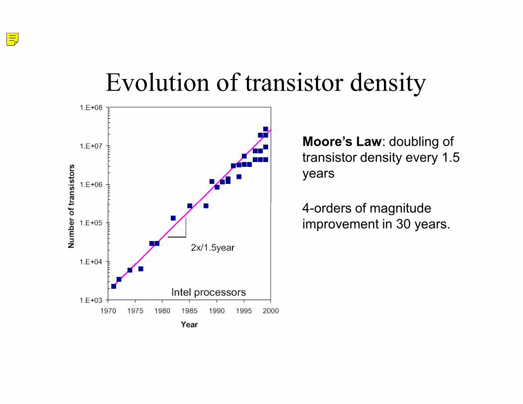
Evolution of transistor density
Moore’s Law: doubling of transistor density every 1.5 years
4orders of magnitude improvement in 30 years.
With transistor size shrinking over time, transistor density in integrated circuits has been increasing very quickly. In fact, it has been increasing exponentially. This graph shows the transistor density of Intel’s microprocessors, from 1971 to 1999. As you can see, the density has increased four orders of magnitude in the last 30 years. This of course is a result of the two-order of magnitude reduction of transistor size in the same period of time. Gordon Moore, one of the founders of Intel, realized in the early 70’s that transistor density was increasing exponentially. He called attention to it and because of this, this fact has become labeled “Moore’s law.” In fact, as you will see today, a lot of data relevant to the microelectronics industry is to be plotted in logarithmic scales as a function of time. These are all corollaries of Moore’s law.
Benefits of increasing transistor integration
Exponential improvements in:
• system performance
• costperfunction,
• powerperfunction, and
• system reliability.
Experimental SOI microprocessor from IBM
Image of microprocessor removed due to copyright restrictions.
Far more important than Moore’s realization of the rate of growth of transistor density was his vision about the consequences of this exponential growth. These are exponential improvements in systems performance, the cost per function, the power consumed in realizing each function, and the reliability of the overall system. It is the combination of all these that has caused the revolutionary impact of microelectronics on human society today. I want to say a few words about system performance and cost per function.
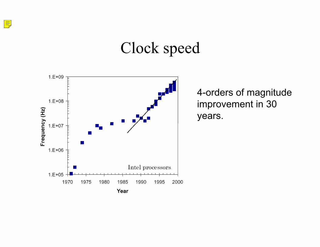
Clock speed
4orders of magnitude improvement in 30 years.
A crude measure of system performance in a logic system is the clock frequency. This is the rate at which logic operations are performed. This graph shows the clock frequency of Intel’s microprocessors as a function of time. There has been an increase of four orders of magnitude over the last 30 years. In the next year or two, we will have microprocessors running at 1 GHz. The four orders of magnitude improvement in clock frequency in the face of a two order of magnitude reduction of transistor size begs a comment. As I will show later on, transistor current drivability improves roughly linearly with size scaling. But the capacitance that each transistor presents also scales down linearly. Hence there is a quadratic improvement in overall system speed.

Transistor cost
3order of magnitude reduction in 30 years.
Let us briefly talk about cost. Here is the cost per transistor in Intel’s processors as a function of time in a semilog scale. In the last 30 years, the cost of a transistor in a logic IC has dropped three orders of magnitude from about 10 cents to 10 millicents of a US dollar. Of course, users do not care about the cost of transistors, but the cost of the functions that the transistors perform. So the next graph shows the cost per megahertz.

Cost per function
4order of magnitude reduction in 30 years.years.
This graph shows a reduction of about four orders of magnitude in the cost per megahertz in Intel’s processors. When you add to it the nearly one order of magnitude increase in word width from 4 bits to 32 bits and many improvements in chip architecture, it is not difficult to see a picture that is broadly consistent with the million-fold improvement that the figure of Kurzweil suggested at the beginning.

Keys to success of digital microelectronics: I. Silicon
• Cheap and abundant
• Amazing mechanical, chemical and electronic properties
• Probably, the material best known to humankind
I now want to talk for a few minutes about the keys behind the success of the microelectronics technology. I want to talk about three of them. The first key is the metal oxide-semiconductor field-effect transistor, which is the transistor structure at the center of the microelectronics revolution. The MOSFET has at its heart a polysilicon gate (formerly metal), oxide semiconductor structure. Applying a voltage to the gate above a certain threshold voltage attracts electrons to the interface of the semiconductor and the oxide. These electrons can then close the switch between two other pools of electrons called source and drain located nearby, so that current can flow from one to the other. In essence, a MOSFET is a switch that is activated electronically. If the voltage applied to the gate is below the threshold voltage, the switch is open. If it is above, the switch is closed. In this manner, one can do logic.

Keys to success of digital microelectronics: II. MOSFET
MetalOxideSemiconductor MOSFET = switch
FieldEffect Transistor
Good gain, isolation, and speed
I now want to talk for a few minutes about the keys behind the success of the microelectronics technology. I want to talk about three of them. The first key is the metal oxide-semiconductor field-effect transistor, which is the transistor structure at the center of the microelectronics revolution. The MOSFET has at its heart a polysilicon gate (formerly metal), oxide semiconductor structure. Applying a voltage to the gate above a certain threshold voltage attracts electrons to the interface of the semiconductor and the oxide. These electrons can then close the switch between two other pools of electrons called source and drain located nearby, so that current can flow from one to the other. In essence, a MOSFET is a switch that is activated electronically. If the voltage applied to the gate is below the threshold voltage, the switch is open. If it is above, the switch is closed. In this manner, one can do logic.
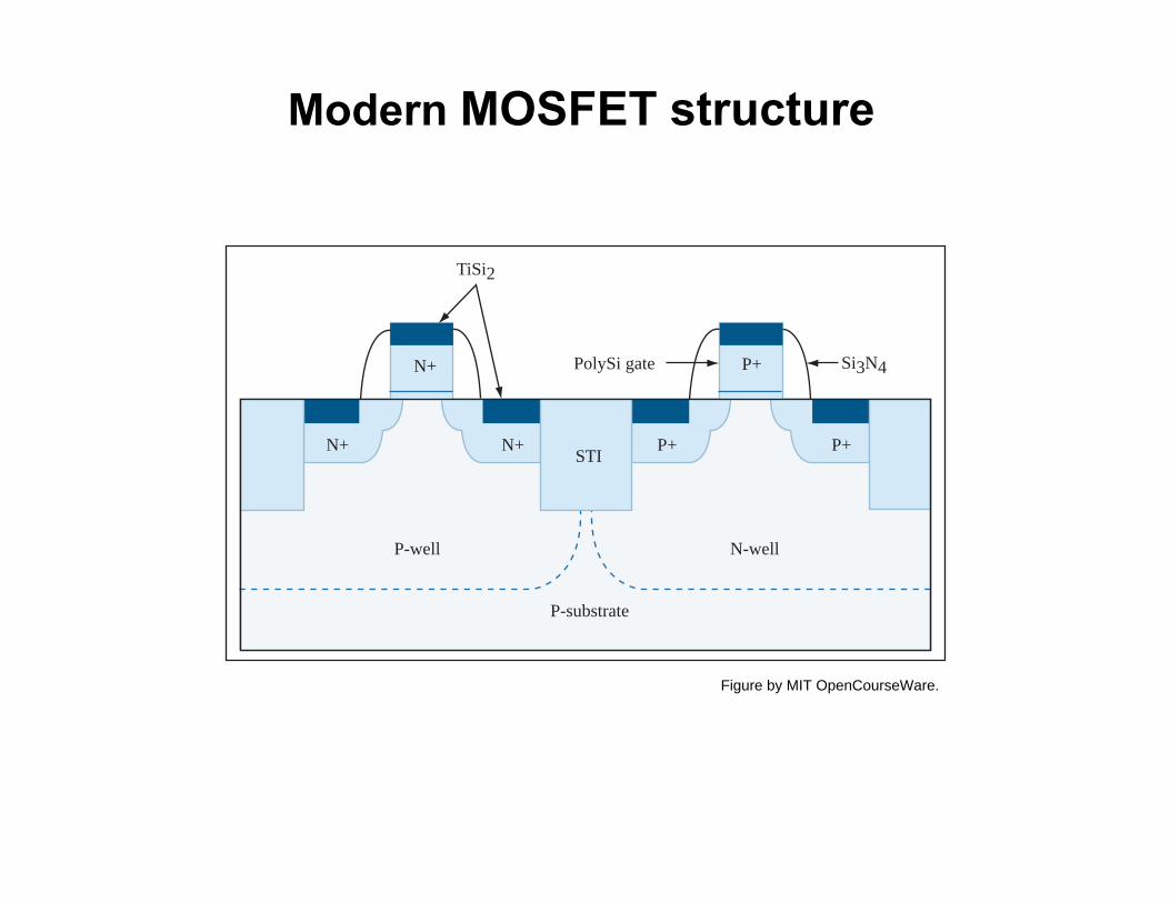
Modern MOSFET structure
P-substrate
N-well
P+ P+
P+
N+
N+
N+
P-well
TiSi2
Si3N4PolySi gate
STI
Figure by MIT OpenCourseWare.
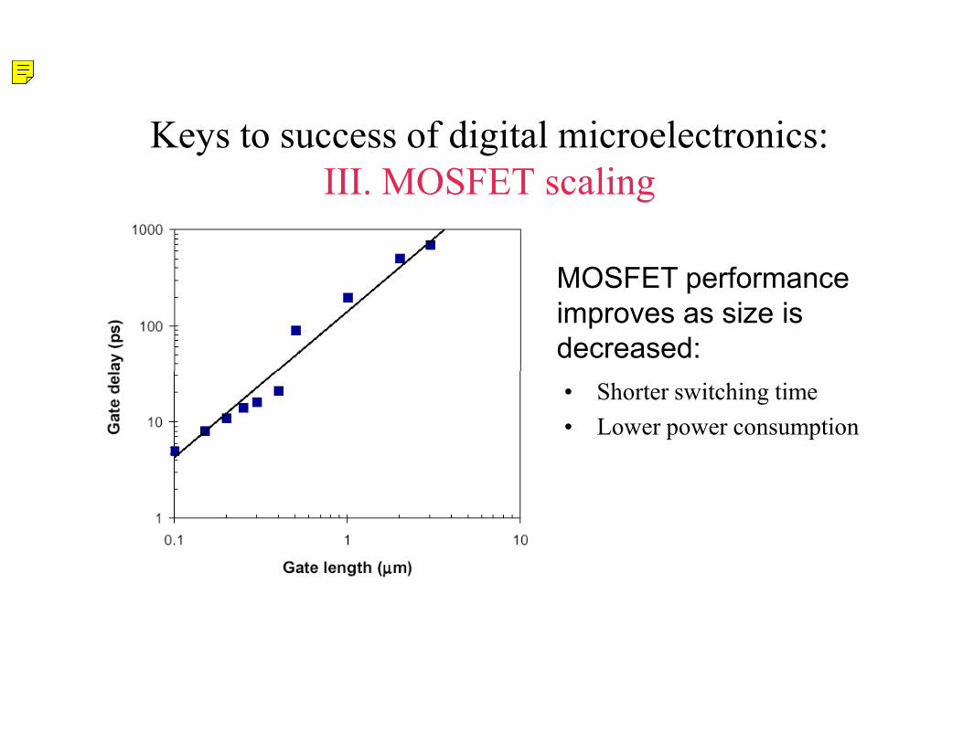
Keys to success of digital microelectronics:
MOSFET performance improves as size is decreased: • Shorter switching time
• Lower power consumption
III. MOSFET scaling
A second key to the success of Si microelectronics is the fact that the MOSFET operation as a switch improves as it is scaled down in size. It improves in two ways. First, the time it takes for the switch to activate is reduced. Second, the energy needed to activate the switch is also reduced. This figure illustrates the first point. It shows the switching time of MOSFETs as a function of the gate length, its critical dimension. As I mentioned earlier, the reduction in switching time is roughly quadratic with the gate length. Indeed, MOSFET performance improves very quickly as its size is reduced.

Keys to success of digital microelectronics: IV. CMOS
CMOS: Complementary MetalOxideSemiconductor
• “Complementary” switch activates with V<0. • Logic without DC power consumption.
The third key to success is called CMOS for complementary metal-oxide semiconductor. That means that we actually have not one but two types of MOSFETs, one that activates with voltage above a certain value and another complementary one which activates with voltages below a different value. This allows what is called complementary logic. This basically means that when one switch is closed, the other one is open. In this manner, it is possible to do logic operations without having a direct shunt between the power supply and ground avoiding DC current. No other logic family does this. This is the key behind the enormous circuit densities that I talked about earlier. Power dissipation has imposed a rigorous density limitation to all other logic families.

•
Keys to success of digital microelectronics: V. Microfabrication technology
• Tight integration of dissimilar devices with good isolation
• Fabrication of extremely small Fabrication of extremely smallstructures, precisely and reproducibly
• Highvolume manufacturing of complex systems with high yield.
1 Gbit DRAM from IBM
Image of DRAM removed due to copyright restrictions.
The third key to success is called CMOS for complementary metal-oxide semiconductor. That means that we actually have not one but two types of MOSFETs, one that activates with voltage above a certain value and another complementary one which activates with voltages below a different value. This allows what is called complementary logic. This basically means that when one switch is closed, the other one is open. In this manner, it is possible to do logic operations without having a direct shunt between the power supply and ground avoiding DC current. No other logic family does this. This is the key behind the enormous circuit densities that I talked about earlier. Power dissipation has imposed a rigorous density limitation to all other logic families.

Keys to success of digital microelectronics: VI. Circuit engineering
• Simple device models that: – are based on physics – allow analog and digital circuit design – permit assessment of impact of device variations on circuit performance
• Circuit design techniques that: – are tolerant to logic level fluctuations, noise and crosstalk – are insensitive to manufacturing variations – require little power consumption
The third key to success is called CMOS for complementary metal-oxide semiconductor. That means that we actually have not one but two types of MOSFETs, one that activates with voltage above a certain value and another complementary one which activates with voltages below a different value. This allows what is called complementary logic. This basically means that when one switch is closed, the other one is open. In this manner, it is possible to do logic operations without having a direct shunt between the power supply and ground avoiding DC current. No other logic family does this. This is the key behind the enormous circuit densities that I talked about earlier. Power dissipation has imposed a rigorous density limitation to all other logic families.
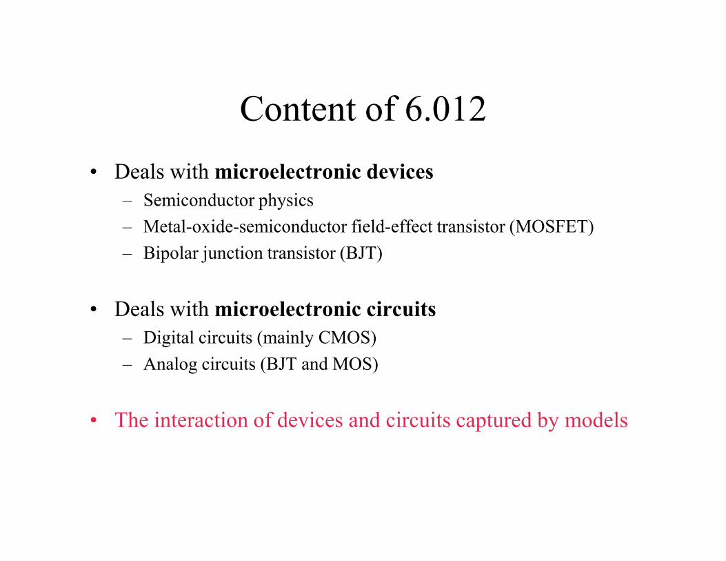
Content of 6.012
• Deals with microelectronic devices – Semiconductor physics
– Metaloxidesemiconductor fieldeffect transistor (MOSFET) – Bipolar junction transistor (BJT)
• Deals with microelectronic circuits – Digital circuits (mainly CMOS) – Analog circuits (BJT and MOS)
• The interaction of devices and circuits captured by models

MIT OpenCourseWarehttp://ocw.mit.edu
6.012 Microelectronic Devices and Circuits Spring 2009
For information about citing these materials or our Terms of Use, visit: http://ocw.mit.edu/terms.


