RCS reduction of integrated antenna arrays with resistive ...

Engineering Science and Technology, an International Journal 19 (2016) 1360–1367
Contents lists available at ScienceDirect
Engineering Science and Technology,an International Journal
journal homepage: www.elsevier .com/locate / jestch
Full Length Article
Miniaturized microstrip antenna array using defected ground structurewith enhanced performance
http://dx.doi.org/10.1016/j.jestch.2016.03.0072215-0986/� 2016 Karabuk University. Publishing services by Elsevier B.V.This is an open access article under the CC BY-NC-ND license (http://creativecommons.org/licenses/by-nc-nd/4.0/).
⇑ Corresponding author.E-mail addresses: [email protected] (R.A. Pandhare), [email protected]
(P.L. Zade), [email protected] (M.P. Abegaonkar).
Peer review under responsibility of Karabuk University.
Rashmi A. Pandhare a,⇑, Prasanna L. Zade b, Mahesh P. Abegaonkar c
aDepartment of Electronics Engineering, Datta Meghe Institute of Engineering, Technology & Research, Wardha, IndiabDepartment of Electronics & Telecommunication Engineering, YCCE, Nagpur, IndiacCenter for Applied Research in Electronics, Indian Institute of Technology, New Delhi, India
a r t i c l e i n f o a b s t r a c t
Article history:Received 28 December 2015Revised 29 March 2016Accepted 29 March 2016Available online 16 April 2016
Keywords:Microstrip patch antenna arrayDefected ground structureMiniaturization
The aim of this work is to obtain a miniaturized microstrip patch antenna array using defected groundstructure (DGS) for S band at 2.2 GHz. Initially the patch antenna array designed at C band resonatesat 5.2 GHz. The proposed DGS is integrated in the ground plane of the patch antenna array for size reduc-tion. However, this miniaturization is at the cost of gain of the antenna. In order to improve the gain ofthis miniaturized radiator, the patch radiator is further modified to retain its radiation properties. Finally,the resonance frequency of an initial microstrip antenna array shifts from 5.2 GHz to 2.2 GHz and withbetter performance miniaturization up to 83% with respect to conventional microstrip antenna issuccessfully accomplished. A prototype of the antenna was fabricated with the RT-Duroid substrate.This technique is validated experimentally and measured results were in good agreement with simulatedresults.� 2016 Karabuk University. Publishing services by Elsevier B.V. This is an open access article under the CC
BY-NC-ND license (http://creativecommons.org/licenses/by-nc-nd/4.0/).
1. Introduction
Microstrip antennas are quite an obvious choice for wirelessdevices because of their properties, and several advantages ascompared to other bulky type of antennas. Some of the mainadvantages of microstrip antenna are that it has low fabricationcost, light weight, low volume, and low profile configuration thatcan be made conformal, it can be easily mounted on rockets,missiles and any conformal shaped satellites without major modi-fications and arrays of these antennas can simply be produced [1].However, the microstrip patch antennas suffer from a number ofdisadvantages as patch length is around half a wavelength.
In recent years, the miniaturization of antennas has becomemore and more important due to the increasing demand for smallantennas as the rapid development in wireless communications.Many efforts have also been made in order to achieve the sizereduction like using planar inverted F antenna structure (PIFA)[2] or using a dielectric substrate of high permittivity [3], defectedmicrostrip structure (DMS) [4], defected ground structure (DGS)[5], or a combination of them.
Mainly DGS is an etched periodic or non-periodic cascadedconfiguration defect in ground of a planar transmission line (e.g.,microstrip, coplanar and conductor backed coplanar wave guide)which disturbs the shield current distribution in the ground planebecause of the defect in the ground .The defect geometry is easy toimplement and does not need a large area. These features enablesuch structures to acquire a great relevance in microwave circuitdesign [6]. In particular, DGS is employed to design microstripantennas for different applications, for instance, cross polarization,mutual coupling reduction in antenna arrays and harmonic sup-pression. Moreover, DGS has been widely used in the developmentof miniaturized antennas [7].
In this paper DGS is used to design a miniaturized microstrippatch antenna array as compared with a conventional one. Initiallythe proposed typical rectangular microstrip patch array antennadesigned at C band, resonates at 5.2 GHz. However it is furtherminiaturized by introducing the new DGS to shift the resonancefrequency from C band to S band keeping the physical volume ofthe antenna constant and hence the size reduction about 79% com-pared with the conventional one is carried out. This size reductionsignificantly reduces the gain and degrades the antenna perfor-mance due to the increase in ohmic losses. Further in order toenhance the antenna performance with size reduction, it has beenproposed to modify the patch radiator of the typical rectangularantenna with the same DGS structure. Finally, the modified

R.A. Pandhare et al. / Engineering Science and Technology, an International Journal 19 (2016) 1360–1367 1361
E-shape patch antenna with same DGS gives the size reduction ofabout 83% with the minimum reduction in gain and betterimpedance matching compared with the conventional one.
Fig. 2. Simulated S11 of the patch antenna array resonating at 5.2 GHz.
2. Microstrip patch antenna array resonating at 5.2 GHz
The proposed 2 by 1 element array microstrip patch antenna isshown in Fig. 1. In this design the substrate RT Duroid was useddue to its advantages. The substrate height was 0.762 mm withdielectric constant of 2.2 and the loss tangent was 0.0004. Thedimensions of the antenna were optimized by using CST Micro-wave Studio tool. On the top of the substrate, a metal patch withdimension Lp = 18.6 mm and Wp = 22.80 was connected to 50ohm feed line with an inset, the dimensions of inset feed wereLi = 11 mm andWi = 2.3 mm. The microstrip line 1:2 power divideris used to feed the two antennas and hence the line widths areadjusted according to the power division. The simulation resultof reference antenna is shown in Fig. 2. The polar radiation plotssimulated at / = 90� and / = 0� are shown in Figs. 3 and 4respectively.
The design and simulation of the proposed antenna have beencarried out. Fig. 2 shows S11 of the antenna without any DGS inground plane resonates at frequency 5.2 GHz (C band) with thegain 9.9 dBi. The objective of this work is to miniaturize antennausing DGS without degradation of antenna performance.
Fig. 3. Reference antenna radiation pattern at Phi = 90.
3. Defected ground structure (DGS)
The defected ground structure (DGS) and the Electromagneticband gap structures (PBG) are the two different types of the genericstructures mostly used for the design of compact and high perfor-mance microwave components [8]. These structures are employedto reject unwanted frequency and circuit size reduction. DGS is anetched lattice of certain shape located on the ground plane.The performance of microstrip antennas and their array canbe enhanced by introducing the defects in the ground plane [9].The shape of the defect may be changed from the simple shapeto the complicated shape for better performance. The DGS equiva-lent circuit consists of a parallel tuned circuit in series with thetransmission line to which it is coupled as shown in Fig. 5.
The different shapes of DGS structure have the same role andsame characteristics of slow wave effect and high impedance, bandrejection, miniaturization of size with the same equivalent circuit[10]. However to improve the circuit performance of antenna theshape of DGS can be further change or modified. In this workwe have employed DGS in metallic ground plane for antenna
Fig. 1. Reference 2 by 1 element array antenna without DGS.
Fig. 4. Reference antenna radiation pattern at Phi = 0.
Fig. 5. Equivalent circuit of DGS.
miniaturization. When DGS is introduced in a microstrip antenna,the defect geometry etched in the ground plane disturbs its currentdistribution. This disturbance affects the transmission line charac-teristics, such as the line capacitance and inductance. In other

Fig. 6. Microstrip 2 by 1 element array antenna with DGS.
Fig. 7. Back-view of microstrip 2 by 1 element array antenna with DGS.
Fig. 8. DGS geometry (K = 20 mm, D = 14 mm A = B = C = 1 mm).
Fig. 9. Simulated S11 of the patch antenna with DGS resonating at 2.4 GHz.
Fig. 10. Simulated S11 without step A and B.
Fig. 11. Radiation pattern for the DGS antenna at Phi = 90.
1362 R.A. Pandhare et al. / Engineering Science and Technology, an International Journal 19 (2016) 1360–1367
words, introducing DGS in a microstrip antenna can result in anincrease of the effective capacitance and inductance which influ-ences the input impedance and current flow of the antenna [11]thus reducing its size with respect to a given resonance frequency.
4. Microstrip patch antenna array with DGS
In order to shift the resonance frequency of the conventionalmicrostrip antenna array (Fig. 2) from C band to S band, initiallya new DGS shape is etched on the metallic ground plane of theantenna shown in Figs. 6 and 7.
Fig. 8 shows the detail geometry of DGS with the specifieddimensions. Fig. 9 shows the antenna performance with DGS. Itis observed that the resonance frequency has been significantlyinfluenced by the DGS and it has been shifted from 5.2 GHz to2.4 GHz without changing physical dimension or distance betweenthe antennas.

Table 1Size comparison of antenna resonating at 2.4 GHz.
Frequency Conventional patch sizewithout DGS
Conventional patchsize with DGS
Sizereduction
2.4 GHz 2065.33 mm2 424 mm2 79%
Fig. 12. Top view of the patch antenna (Wp = 22.80 mm, Lp = 18.6, Wi = 2.3 mm,Lps = 12 mm).
Table 2Comparison of E-shaped patch antenna with regular rectangular antenna withoutDGS.
Patch shape Regular rectangularshaped antenna
Modified E-shapedpatch antenna
Resonant Freq. 5.2 GHz 5.2 GHzS11 �18.32 �31.07Bandwidth 100 MHz 120 MHzGain 9.8 10.89
Fig. 13. Modified patch shaped antenna with DGS.
Table 3Comparison of E-shaped patch antenna with regular rectangular antenna with DGS.
Patch shape Rectangular shapedantenna with DGS
E-shaped patchantenna with DGS
Reduced Freq. 2.4 GHz 2.2 GHzS11 �17.06 �32.36Bandwidth 100 MHz 120 MHzGain 1.93 4.8% size reduction 79% 83%
Fig. 14. Simulated S11 of the modified patch antenna with DGS resonating at2.2 GHz.
Table 4Size comparison of antenna resonating at 2.2 GHz.
Frequency Conventional patch sizewithout DGS (in mm2)
Modified E-shape patchsize with DGS (in mm2)
% sizereduction
2.4 GHz 2459.99 424 83%
R.A. Pandhare et al. / Engineering Science and Technology, an International Journal 19 (2016) 1360–1367 1363
The effect of adding or removing the step A, B and C from thefinal new DGS structure (Fig. 8) is also illustrated in order to clarifythe consequence of DGS shape on antenna for size reduction.Fig. 10 shows the antenna performance by removal of steps Aand B from the specified final DGS geometry. It has been observedthat the resonance frequency has been shifted to 3 GHz by removalof step A with the gain 4.42 dBi and by removal of step A as well asB the resonance frequency has been shifted to 3.6 GHz with thegain of 5.5 dBi. With the presence of all steps the antenna resonatesat 2.4 GHz with the gain 1.9 dBi as shown in Fig. 11. Also the effectsof the DGS position on the antenna characteristics have been stud-ied by changing the DGS at different positions. From the simulationresult it has been observed that as the DGS position shifted below
with respect to current position, resonating frequency shifts at thehigher side i.e. 3.2–3.8 GHz. Finally from the simulation result(Fig. 9) it can be revealed that the specified DGS structure withthe presence of all steps (A, B and C) along with the current posi-tion gives maximum best possible size reduction, however byremoval of the steps or by changing the DGS position the antennaresonates at higher frequencies i.e. 3 GHz, 3.2 GHz, 3.6 GHz or3.8 GHz which reduces the percentage of overall size reduction.
Table 1 shows the actual size required to design a microstrippatch antenna which resonates at a frequency of 2.4 GHz and alsothe amount of size reduction using DGS. This gives the overall sizereduction of 79%. Although the physical size of the antenna array issame, it now works at a lower frequency hence in terms of wave-length at new frequency the antenna size is reduced. It is alsorevealed from the result that with miniaturization the gain of theantenna is reduced to 1.94 dBi as shown in Fig. 11 this is mainlybecause with DGS in the ground plane, the antenna will radiateon both sides of the ground plane due to the aperture efficiencyresulting in high back radiation level which explains the maximumgain reduction. In fact one of the major problems in microstripantenna applications is to reduce the size with good performance.However, this miniaturization is at the cost of gain of the antenna.In order to improve the gain of this miniaturized antenna, wefurther modified the patch radiator keeping the physical volumeof the antenna constant with the same DGS structure to retain itsradiation properties.

Fig. 15. Radiation pattern for the modified DGS antenna.
Fig. 16. Current distribution of conventional antenna without DGS.
Fig. 17. Current distribution of patch antenna
Fig. 18. Current distribution of modified patch antenna
1364 R.A. Pandhare et al. / Engineering Science and Technology, an International Journal 19 (2016) 1360–1367
5. Modified patch shape to enhanced antenna performance
The proposed antenna is shown in Fig. 12. In order to enhancethe performance of the antenna, two slots are introduced on thepatch radiator keeping the physical volume of the antennaconstant. Initially, the performance of the antenna with the slotson patch without DGS structured was observed. The modifiedE-shape patch antenna gives better results compared to regularrectangular patch shaped antenna as shown in Table 2. Furtherthe same DGS structure is etched on the ground plane of themodified patch shaped antenna as shown in Fig. 13.
The modified shape of the typical rectangular patch antennawith the same DGS structure has improved the gain of the antennawith the better impedance matching as observed from Table 3. Inthe original regular rectangular antenna designed to resonate at5.2 GHz with the specified area of 424 mm2 and without changingthe physical dimension or distance between the antennas the oper-ation frequency shifts from the C band to the S band with the use ofDGS. Fig. 14 shows S11 of the E-shaped antenna with DGS in theground plane resonating at a frequency of 2.2 GHz. Table 4 showsthe actual size required to design a microstrip patch antenna whichresonates at a frequency of 2.2 GHz and also the amount of sizereduction using DGS. This gives the overall size reduction of 83%without much degradation of the antenna performance.
The radiation pattern as shown in Fig. 15 is obtained. By com-paring the radiation pattern of the regular rectangular patchshaped antenna with DGS (Fig. 11) with the radiation pattern ofthe modified patch shaped antenna with the same DGS structureas shown in Fig. 15, it is observed that there is a high back radiationin the regular rectangular antenna by employing the DGS, whereasthe modified E-shaped patch antenna with the same DGS reducesthe back radiation and hence increases the gain from 1.94 dBi to
with DGS, (a) front view, (b) back view.
with the same DGS (a) front view, (b) back view.
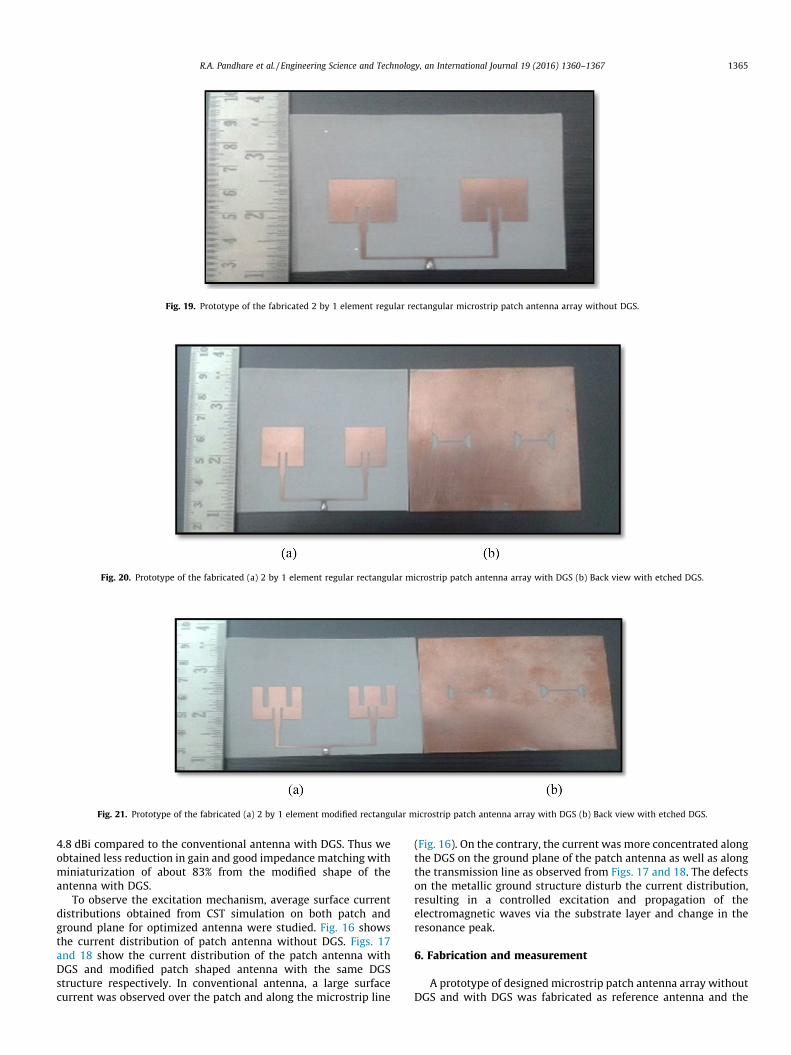
Fig. 19. Prototype of the fabricated 2 by 1 element regular rectangular microstrip patch antenna array without DGS.
Fig. 20. Prototype of the fabricated (a) 2 by 1 element regular rectangular microstrip patch antenna array with DGS (b) Back view with etched DGS.
Fig. 21. Prototype of the fabricated (a) 2 by 1 element modified rectangular microstrip patch antenna array with DGS (b) Back view with etched DGS.
R.A. Pandhare et al. / Engineering Science and Technology, an International Journal 19 (2016) 1360–1367 1365
4.8 dBi compared to the conventional antenna with DGS. Thus weobtained less reduction in gain and good impedance matching withminiaturization of about 83% from the modified shape of theantenna with DGS.
To observe the excitation mechanism, average surface currentdistributions obtained from CST simulation on both patch andground plane for optimized antenna were studied. Fig. 16 showsthe current distribution of patch antenna without DGS. Figs. 17and 18 show the current distribution of the patch antenna withDGS and modified patch shaped antenna with the same DGSstructure respectively. In conventional antenna, a large surfacecurrent was observed over the patch and along the microstrip line
(Fig. 16). On the contrary, the current was more concentrated alongthe DGS on the ground plane of the patch antenna as well as alongthe transmission line as observed from Figs. 17 and 18. The defectson the metallic ground structure disturb the current distribution,resulting in a controlled excitation and propagation of theelectromagnetic waves via the substrate layer and change in theresonance peak.
6. Fabrication and measurement
A prototype of designed microstrip patch antenna array withoutDGS and with DGS was fabricated as reference antenna and the
1366 R.A. Pandhare et al. / Engineering Science and Technology, an International Journal 19 (2016) 1360–1367
proposed antenna respectively. We have used RT-Duroid substratewith relative dielectric constant of 2.2 and the thickness of0.762 mm. Fig. 19 shows the size of regular rectangular microstrippatch antenna array without DGS. Fig. 20(a) and (b) shows size ofthe top and back view respectively of regular rectangular micro-strip patch antenna array with DGS. Fig. 21(a) and (b) shows thesize of the top and back view respectively of the modified micro-strip patch antenna array with the same DGS.
In order to measure the various parameters of the antenna wehave been employing MS2028C vector network analyzer, withfrequency range limited to 20 GHz. Thus S11 parameter was
Fig. 22. Measurement and simulation result of regular rectangular microstrip patchantenna array without DGS (resonating at 5.2 GHz).
Fig. 23. Measurement and simulation result of regular rectangular microstrip patchantenna array with DGS (resonating at 2.4 GHz).
Fig. 24. Measurement and simulation result of modified microstrip patch antennaarray with same DGS (resonating at 2.2 GHz).
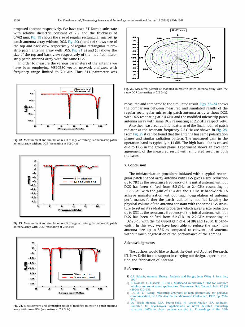
Fig. 25. Measured pattern of modified microstrip patch antenna array with thesame DGS (resonating at 2.2 GHz).
measured and compared to the simulated result. Figs. 22–24 showsthe comparison between measured and simulated results of theregular rectangular microstrip patch antenna array without DGS,with DGS resonating at 2.4 GHz and the modified microstrip patchantenna array with same DGS resonating at 2.2 GHz respectively.
Also the measured radiation patterns of the final modified patchradiator at the resonant frequency 2.2 GHz are shown in Fig. 25.From Fig. 25 it can be found that the antenna has same polarizationplanes and similar radiation pattern. The measured gain in theoperation band is typically 4.14 dBi. The high back lobe is causeddue to DGS in the ground plane. Experiment shows an excellentagreement of the measured result with simulated result in boththe cases.
7. Conclusion
The miniaturization procedure initiated with a typical rectan-gular patch shaped array antenna with DGS gives a size reductionup to 79% as the resonance frequency of the initial antenna withoutDGS has been shifted from 5.2 GHz to 2.4 GHz resonating at�17.86 dB with the gain of 1.94 dBi and 100 MHz bandwidth. Toachieve miniaturization without much degradation of antennaperformance, further the patch radiator is modified keeping thephysical volume of the antenna constant with the same DGS struc-ture to retain its radiation properties which gives a size reductionup to 83% as the resonance frequency of the initial antenna withoutDGS has been shifted from 5.2 GHz to 2.2 GHz resonating at�32.26 dB with the measured gain of 4.14 dBi and 120 MHz band-width. In this way we have been able to reduce the maximumantenna size up to 83% as compared to conventional antennawithout much degradation of the performance of the antenna.
Acknowledgments
The authors would like to thank the Centre of Applied Research,IIT, New Delhi for the support in carrying out design, experimenta-tion and fabrication of Antenna.
References
[1] C.A. Balanis, Antenna Theory: Analysis and Design, John Wiley & Sons Inc.,1997.
[2] D. Nashaat, H. Elsadek, H. Ghali, Multiband miniaturized PIFA for compactwireless communication applications, Microwave Opt. Technol. Lett. 42 (3)(2004) 230–235.
[3] T.K. Lo, Y. Hwang, Microstrip antennas of high permittivity for personalcommunication, in: 1997 Asia Pacific Microwave Conference, 1997, pp. 253–256.
[4] J.A. Tirado-Mendez, M.A. Peyrot-Solis, H. Jardon-Aguilar, E.A. Andrade-Gonzalez, M. Reyes-Ayala, Applications of novel defected microstripstructure (DMS) in planar passive circuits, in: Proceedings of the 10th

R.A. Pandhare et al. / Engineering Science and Technology, an International Journal 19 (2016) 1360–1367 1367
WSEAS International Conference on CIRCUITS, Vouliagmeni, Athens, Greece,July 10–12, 2006, pp. 336–369.
[5] M. Chakraborty, B. Rana, P.P. Sarkar, A. Das, Size reduction of microstripantenna with slots and defected ground structure, Int. J. Electron. Eng. 4 (1)(2012) 61–64.
[6] L.H. Weng, Y.C. Guo, X.W. Shi, X.Q. Chen, An overview on defected groundstructure, Prog. Electromagnet. Res., B 7 (2008) 173–189.
[7] Hanae Elftouhl, Naima A. Touhami, Mohamed Aghoutane, Miniaturizedmicrostrip patch antenna with defected ground structure, Prog. Electro-magnet. Res., C 55 (2014) 25–33.
[8] F. Yang, Y. Rahmat samii, Electromagnetic Band Gap Structures in AntennaEngineering, Cambridge University Press, USA, 2009.
[9] Munish Kumar, Vandana Nath, Analysis of low mutual coupling compactmulti-band microstrip patch antenna and its array using defected groundstructure, Eng. Sci. Technol. Int. J. (2015). jestch.2015.12.003.
[10] Ashwini K. Arya, M.V. Kartikeyan, A. Patnaik, Defected ground structure in theperspective of microstrip antenna, Frequenz 64 (5–6) (2010) 79–84.
[11] A.K. Arya, A. Patnaik, M.V. Kartikeyan, Microstrip patch antenna with skew-Fshaped DGS for dual band operation, Prog. Electromagnet. Res., M 19 (2011)147–160.


![A Microstrip Patch Antenna with Defected Ground …coupling of the multi-band microstrip patch array is reduced. In [19], a defected ground structured compact plus shaped slot loaded](https://static.fdocuments.in/doc/165x107/5fd20002ebbc7a58c62a1838/a-microstrip-patch-antenna-with-defected-ground-coupling-of-the-multi-band-microstrip.jpg)